EP2633102B1 - KOLLOIDALE NANOSHEETS und deren Verwendung - Google Patents
KOLLOIDALE NANOSHEETS und deren Verwendung Download PDFInfo
- Publication number
- EP2633102B1 EP2633102B1 EP11782179.3A EP11782179A EP2633102B1 EP 2633102 B1 EP2633102 B1 EP 2633102B1 EP 11782179 A EP11782179 A EP 11782179A EP 2633102 B1 EP2633102 B1 EP 2633102B1
- Authority
- EP
- European Patent Office
- Prior art keywords
- colloidal
- nanosheet
- nanosheets
- semiconductor
- initial
- Prior art date
- Legal status (The legal status is an assumption and is not a legal conclusion. Google has not performed a legal analysis and makes no representation as to the accuracy of the status listed.)
- Active
Links
Images


Classifications
-
- B—PERFORMING OPERATIONS; TRANSPORTING
- B82—NANOTECHNOLOGY
- B82Y—SPECIFIC USES OR APPLICATIONS OF NANOSTRUCTURES; MEASUREMENT OR ANALYSIS OF NANOSTRUCTURES; MANUFACTURE OR TREATMENT OF NANOSTRUCTURES
- B82Y30/00—Nanotechnology for materials or surface science, e.g. nanocomposites
-
- C—CHEMISTRY; METALLURGY
- C30—CRYSTAL GROWTH
- C30B—SINGLE-CRYSTAL GROWTH; UNIDIRECTIONAL SOLIDIFICATION OF EUTECTIC MATERIAL OR UNIDIRECTIONAL DEMIXING OF EUTECTOID MATERIAL; REFINING BY ZONE-MELTING OF MATERIAL; PRODUCTION OF A HOMOGENEOUS POLYCRYSTALLINE MATERIAL WITH DEFINED STRUCTURE; SINGLE CRYSTALS OR HOMOGENEOUS POLYCRYSTALLINE MATERIAL WITH DEFINED STRUCTURE; AFTER-TREATMENT OF SINGLE CRYSTALS OR A HOMOGENEOUS POLYCRYSTALLINE MATERIAL WITH DEFINED STRUCTURE; APPARATUS THEREFOR
- C30B29/00—Single crystals or homogeneous polycrystalline material with defined structure characterised by the material or by their shape
- C30B29/10—Inorganic compounds or compositions
- C30B29/46—Sulfur-, selenium- or tellurium-containing compounds
-
- C—CHEMISTRY; METALLURGY
- C30—CRYSTAL GROWTH
- C30B—SINGLE-CRYSTAL GROWTH; UNIDIRECTIONAL SOLIDIFICATION OF EUTECTIC MATERIAL OR UNIDIRECTIONAL DEMIXING OF EUTECTOID MATERIAL; REFINING BY ZONE-MELTING OF MATERIAL; PRODUCTION OF A HOMOGENEOUS POLYCRYSTALLINE MATERIAL WITH DEFINED STRUCTURE; SINGLE CRYSTALS OR HOMOGENEOUS POLYCRYSTALLINE MATERIAL WITH DEFINED STRUCTURE; AFTER-TREATMENT OF SINGLE CRYSTALS OR A HOMOGENEOUS POLYCRYSTALLINE MATERIAL WITH DEFINED STRUCTURE; APPARATUS THEREFOR
- C30B29/00—Single crystals or homogeneous polycrystalline material with defined structure characterised by the material or by their shape
- C30B29/10—Inorganic compounds or compositions
- C30B29/16—Oxides
-
- C—CHEMISTRY; METALLURGY
- C30—CRYSTAL GROWTH
- C30B—SINGLE-CRYSTAL GROWTH; UNIDIRECTIONAL SOLIDIFICATION OF EUTECTIC MATERIAL OR UNIDIRECTIONAL DEMIXING OF EUTECTOID MATERIAL; REFINING BY ZONE-MELTING OF MATERIAL; PRODUCTION OF A HOMOGENEOUS POLYCRYSTALLINE MATERIAL WITH DEFINED STRUCTURE; SINGLE CRYSTALS OR HOMOGENEOUS POLYCRYSTALLINE MATERIAL WITH DEFINED STRUCTURE; AFTER-TREATMENT OF SINGLE CRYSTALS OR A HOMOGENEOUS POLYCRYSTALLINE MATERIAL WITH DEFINED STRUCTURE; APPARATUS THEREFOR
- C30B29/00—Single crystals or homogeneous polycrystalline material with defined structure characterised by the material or by their shape
- C30B29/10—Inorganic compounds or compositions
- C30B29/46—Sulfur-, selenium- or tellurium-containing compounds
- C30B29/48—AIIBVI compounds wherein A is Zn, Cd or Hg, and B is S, Se or Te
-
- C—CHEMISTRY; METALLURGY
- C30—CRYSTAL GROWTH
- C30B—SINGLE-CRYSTAL GROWTH; UNIDIRECTIONAL SOLIDIFICATION OF EUTECTIC MATERIAL OR UNIDIRECTIONAL DEMIXING OF EUTECTOID MATERIAL; REFINING BY ZONE-MELTING OF MATERIAL; PRODUCTION OF A HOMOGENEOUS POLYCRYSTALLINE MATERIAL WITH DEFINED STRUCTURE; SINGLE CRYSTALS OR HOMOGENEOUS POLYCRYSTALLINE MATERIAL WITH DEFINED STRUCTURE; AFTER-TREATMENT OF SINGLE CRYSTALS OR A HOMOGENEOUS POLYCRYSTALLINE MATERIAL WITH DEFINED STRUCTURE; APPARATUS THEREFOR
- C30B29/00—Single crystals or homogeneous polycrystalline material with defined structure characterised by the material or by their shape
- C30B29/60—Single crystals or homogeneous polycrystalline material with defined structure characterised by the material or by their shape characterised by shape
-
- C—CHEMISTRY; METALLURGY
- C30—CRYSTAL GROWTH
- C30B—SINGLE-CRYSTAL GROWTH; UNIDIRECTIONAL SOLIDIFICATION OF EUTECTIC MATERIAL OR UNIDIRECTIONAL DEMIXING OF EUTECTOID MATERIAL; REFINING BY ZONE-MELTING OF MATERIAL; PRODUCTION OF A HOMOGENEOUS POLYCRYSTALLINE MATERIAL WITH DEFINED STRUCTURE; SINGLE CRYSTALS OR HOMOGENEOUS POLYCRYSTALLINE MATERIAL WITH DEFINED STRUCTURE; AFTER-TREATMENT OF SINGLE CRYSTALS OR A HOMOGENEOUS POLYCRYSTALLINE MATERIAL WITH DEFINED STRUCTURE; APPARATUS THEREFOR
- C30B7/00—Single-crystal growth from solutions using solvents which are liquid at normal temperature, e.g. aqueous solutions
- C30B7/08—Single-crystal growth from solutions using solvents which are liquid at normal temperature, e.g. aqueous solutions by cooling of the solution
-
- H—ELECTRICITY
- H10—SEMICONDUCTOR DEVICES; ELECTRIC SOLID-STATE DEVICES NOT OTHERWISE PROVIDED FOR
- H10D—INORGANIC ELECTRIC SEMICONDUCTOR DEVICES
- H10D62/00—Semiconductor bodies, or regions thereof, of devices having potential barriers
- H10D62/40—Crystalline structures
-
- H—ELECTRICITY
- H10—SEMICONDUCTOR DEVICES; ELECTRIC SOLID-STATE DEVICES NOT OTHERWISE PROVIDED FOR
- H10F—INORGANIC SEMICONDUCTOR DEVICES SENSITIVE TO INFRARED RADIATION, LIGHT, ELECTROMAGNETIC RADIATION OF SHORTER WAVELENGTH OR CORPUSCULAR RADIATION
- H10F77/00—Constructional details of devices covered by this subclass
- H10F77/10—Semiconductor bodies
- H10F77/12—Active materials
-
- H—ELECTRICITY
- H10—SEMICONDUCTOR DEVICES; ELECTRIC SOLID-STATE DEVICES NOT OTHERWISE PROVIDED FOR
- H10F—INORGANIC SEMICONDUCTOR DEVICES SENSITIVE TO INFRARED RADIATION, LIGHT, ELECTROMAGNETIC RADIATION OF SHORTER WAVELENGTH OR CORPUSCULAR RADIATION
- H10F77/00—Constructional details of devices covered by this subclass
- H10F77/10—Semiconductor bodies
- H10F77/12—Active materials
- H10F77/123—Active materials comprising only Group II-VI materials, e.g. CdS, ZnS or HgCdTe
-
- H—ELECTRICITY
- H10—SEMICONDUCTOR DEVICES; ELECTRIC SOLID-STATE DEVICES NOT OTHERWISE PROVIDED FOR
- H10F—INORGANIC SEMICONDUCTOR DEVICES SENSITIVE TO INFRARED RADIATION, LIGHT, ELECTROMAGNETIC RADIATION OF SHORTER WAVELENGTH OR CORPUSCULAR RADIATION
- H10F77/00—Constructional details of devices covered by this subclass
- H10F77/10—Semiconductor bodies
- H10F77/12—Active materials
- H10F77/126—Active materials comprising only Group I-III-VI chalcopyrite materials, e.g. CuInSe2, CuGaSe2 or CuInGaSe2 [CIGS]
-
- H—ELECTRICITY
- H10—SEMICONDUCTOR DEVICES; ELECTRIC SOLID-STATE DEVICES NOT OTHERWISE PROVIDED FOR
- H10F—INORGANIC SEMICONDUCTOR DEVICES SENSITIVE TO INFRARED RADIATION, LIGHT, ELECTROMAGNETIC RADIATION OF SHORTER WAVELENGTH OR CORPUSCULAR RADIATION
- H10F77/00—Constructional details of devices covered by this subclass
- H10F77/10—Semiconductor bodies
- H10F77/14—Shape of semiconductor bodies; Shapes, relative sizes or dispositions of semiconductor regions within semiconductor bodies
- H10F77/143—Shape of semiconductor bodies; Shapes, relative sizes or dispositions of semiconductor regions within semiconductor bodies comprising quantum structures
- H10F77/1433—Quantum dots
-
- H—ELECTRICITY
- H10—SEMICONDUCTOR DEVICES; ELECTRIC SOLID-STATE DEVICES NOT OTHERWISE PROVIDED FOR
- H10F—INORGANIC SEMICONDUCTOR DEVICES SENSITIVE TO INFRARED RADIATION, LIGHT, ELECTROMAGNETIC RADIATION OF SHORTER WAVELENGTH OR CORPUSCULAR RADIATION
- H10F77/00—Constructional details of devices covered by this subclass
- H10F77/10—Semiconductor bodies
- H10F77/16—Material structures, e.g. crystalline structures, film structures or crystal plane orientations
- H10F77/162—Non-monocrystalline materials, e.g. semiconductor particles embedded in insulating materials
-
- H—ELECTRICITY
- H10—SEMICONDUCTOR DEVICES; ELECTRIC SOLID-STATE DEVICES NOT OTHERWISE PROVIDED FOR
- H10H—INORGANIC LIGHT-EMITTING SEMICONDUCTOR DEVICES HAVING POTENTIAL BARRIERS
- H10H20/00—Individual inorganic light-emitting semiconductor devices having potential barriers, e.g. light-emitting diodes [LED]
- H10H20/80—Constructional details
- H10H20/81—Bodies
- H10H20/817—Bodies characterised by the crystal structures or orientations, e.g. polycrystalline, amorphous or porous
- H10H20/818—Bodies characterised by the crystal structures or orientations, e.g. polycrystalline, amorphous or porous within the light-emitting regions
-
- H—ELECTRICITY
- H10—SEMICONDUCTOR DEVICES; ELECTRIC SOLID-STATE DEVICES NOT OTHERWISE PROVIDED FOR
- H10P—GENERIC PROCESSES OR APPARATUS FOR THE MANUFACTURE OR TREATMENT OF DEVICES COVERED BY CLASS H10
- H10P14/00—Formation of materials, e.g. in the shape of layers or pillars
- H10P14/20—Formation of materials, e.g. in the shape of layers or pillars of semiconductor materials
- H10P14/34—Deposited materials, e.g. layers
- H10P14/3451—Structure
- H10P14/3452—Microstructure
- H10P14/3461—Nanoparticles
-
- B—PERFORMING OPERATIONS; TRANSPORTING
- B82—NANOTECHNOLOGY
- B82Y—SPECIFIC USES OR APPLICATIONS OF NANOSTRUCTURES; MEASUREMENT OR ANALYSIS OF NANOSTRUCTURES; MANUFACTURE OR TREATMENT OF NANOSTRUCTURES
- B82Y40/00—Manufacture or treatment of nanostructures
-
- Y—GENERAL TAGGING OF NEW TECHNOLOGICAL DEVELOPMENTS; GENERAL TAGGING OF CROSS-SECTIONAL TECHNOLOGIES SPANNING OVER SEVERAL SECTIONS OF THE IPC; TECHNICAL SUBJECTS COVERED BY FORMER USPC CROSS-REFERENCE ART COLLECTIONS [XRACs] AND DIGESTS
- Y02—TECHNOLOGIES OR APPLICATIONS FOR MITIGATION OR ADAPTATION AGAINST CLIMATE CHANGE
- Y02E—REDUCTION OF GREENHOUSE GAS [GHG] EMISSIONS, RELATED TO ENERGY GENERATION, TRANSMISSION OR DISTRIBUTION
- Y02E10/00—Energy generation through renewable energy sources
- Y02E10/50—Photovoltaic [PV] energy
- Y02E10/541—CuInSe2 material PV cells
-
- Y—GENERAL TAGGING OF NEW TECHNOLOGICAL DEVELOPMENTS; GENERAL TAGGING OF CROSS-SECTIONAL TECHNOLOGIES SPANNING OVER SEVERAL SECTIONS OF THE IPC; TECHNICAL SUBJECTS COVERED BY FORMER USPC CROSS-REFERENCE ART COLLECTIONS [XRACs] AND DIGESTS
- Y10—TECHNICAL SUBJECTS COVERED BY FORMER USPC
- Y10S—TECHNICAL SUBJECTS COVERED BY FORMER USPC CROSS-REFERENCE ART COLLECTIONS [XRACs] AND DIGESTS
- Y10S977/00—Nanotechnology
- Y10S977/70—Nanostructure
- Y10S977/755—Nanosheet or quantum barrier/well, i.e. layer structure having one dimension or thickness of 100 nm or less
-
- Y—GENERAL TAGGING OF NEW TECHNOLOGICAL DEVELOPMENTS; GENERAL TAGGING OF CROSS-SECTIONAL TECHNOLOGIES SPANNING OVER SEVERAL SECTIONS OF THE IPC; TECHNICAL SUBJECTS COVERED BY FORMER USPC CROSS-REFERENCE ART COLLECTIONS [XRACs] AND DIGESTS
- Y10—TECHNICAL SUBJECTS COVERED BY FORMER USPC
- Y10S—TECHNICAL SUBJECTS COVERED BY FORMER USPC CROSS-REFERENCE ART COLLECTIONS [XRACs] AND DIGESTS
- Y10S977/00—Nanotechnology
- Y10S977/902—Specified use of nanostructure
- Y10S977/932—Specified use of nanostructure for electronic or optoelectronic application
Definitions
- the present invention relates to a nanocrystalline material in the form of sheets, for example obtained by lateral growth of initial nanocrystals or nanosheets produced by continuous introduction of precursors for a predetermined period.
- the invention also relates to the use of the obtained nanocrystals.
- nanostructures having at least one nanometric dimension induces the appearance of new physical properties. These nanostructures have characteristics which may differ significantly from those of the solid material. In particular, there is a modification of the electronic 1 , optical, magnetic 2 or plasmon 3 properties of materials when their dimensions are reduced down to the nanometric scale. These new materials are thus arousing growing interest in fields as varied as optics, electronics and catalysis.
- Colloidal semiconductor nanocrystals in particular have been a subject of much study since the early 1980s. These see their optical properties change when their size reaches nanometric dimensions 4.5 . Their absorbance shifts towards blue and they become fluorescent at a wavelength depending only on the size of the particle considered. Indeed, below a certain size (defined by the excitonic Bohr radius of the material), the effects of quantum confinement are felt and the band gap energy of the semiconductor increases when the size decreases 6 . For CdSe for example, the excitonic Bohr radius is 56 Angström and the energy of the band gap corresponds to 710nm for the solid material.
- the CdSe nanocrystals fluoresce in blue (2nm in diameter), green (3nm in diameter), orange (4nm in diameter) or red (6nm in diameter) 7 .
- Spectroscopy then becomes a privileged tool for characterizing these objects; the average size and the size dispersion of a set of particles can be accessed directly by performing an absorbance or emission spectrum of the sample.
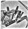
- nanosheets Depending on the geometry of the nanocrystals, it is possible to observe several types of confinement: three-dimensional in the case of a spherical nanocrystal (quantum point) and two-dimensional in the case of a nanowire. Only objects with one-dimensional containment were missing from this list. This would appear for objects of low thickness (a few nanometers, less than the Bohr radius) and lateral dimensions of at least an order of magnitude greater (at least 10nm for example for CdSe). In the following, these objects will be referred to as nanosheets.
- Direct exfoliation is commonly used in order to produce sheets of graphene, hydroxides or oxides (TiO 2 for example).
- the method of preparation generally consists in reducing the interaction energy between the sheets in order to separate them mechanically thereafter.
- One strategy used for ionic compounds is to cause swelling of the inter-sheet space (generally containing positive ions) by exchanging the cations with a highly hindered ion such as tetrabutyl ammonium hydroxide 13 . This swelling weakens the interactions between the layers which can then be separated mechanically by sonication for example.
- the decrease in the interlayer interaction energy can be achieved by using a suitable solvent such as N-methylpyrrolidone 14 .
- a suitable solvent such as N-methylpyrrolidone 14 .
- This type of process always results in the production of mono-sheets a few Angstroms thick.
- the size of the sheets depends on the size of the massive exfoliated object. It is also unthinkable to control the thickness of the nanosheet; this is fixed by the lamellar structure of the starting compound and therefore by its chemical nature.
- This manufacturing method although being extremely general, still has certain limitations. It is in fact impossible to finely control the thickness of the sheets obtained and to obtain a set of sheets all having the same thickness (monodispersity in thickness). In addition, to our knowledge, the possibility of carrying out a subsequent lateral extension of these materials has not been reported.
- a protocol for the synthesis of CdSe nanoplatelets has recently been reported 12 consisting in the rapid injection of an acetate salt into a hot reaction medium containing powdered selenium and a cadmium carboxylate.
- the formation of nanoplatelets is rapid and is accompanied by the unwanted formation of quantum-dots (isotropic colloidal nanocrystals).
- quantum-dots isotropic colloidal nanocrystals.
- Embodiments of the invention which will be described below present methods for two-dimensional growth of semiconductor nanocrystals. These methods make it possible to achieve lateral dimensions greater than one micron while the thickness of the nanosheets is kept constant, controlled down to the atomic monolayer. It is It is also possible to control the thickness of the nanosheets obtained by controlling some of the synthesis parameters such as the nature of the precursors, the reaction temperature and / or the presence of nanocrystals within the reaction medium.
- the new crystal growth process disclosed opposes the paradigm "nucleation / growth by rapid injection of hot precursors" which is currently used in all organic syntheses of colloidal semiconductor nanocrystals.
- the precursors are introduced slowly into the flask.
- the nucleation rate is governed by the temperature of the flask and the rate of injection; the system is moving towards a state of growth at equilibrium in which all the injected precursors are consumed for the growth of the sheets, the initial nucleation allows the existence within the reaction medium of sufficient germs to consume the precursors at any time introduced.
- the final size of the nanosheets (its lateral dimensions) is thus governed by the quantity of precursors introduced.
- the proposed growth mode is also opposed to the descriptions of syntheses of nanosheets by the so-called "soft templating" method in which a lamellar complex present in solution (a role which may be played by the acetate salt) guides growth. towards the formation of nanosheets.
- a precursor solution comprising a finely ground and well dispersed acetate salt is slowly introduced into the reaction medium, which may simply be a hot organic solvent without an acetate salt.
- the thickness of the sheets By controlling the temperature and the nature of the precursors, it is therefore possible to control the thickness of the sheets while their concentration is controlled by the injection speed and the lateral dimensions are controlled by the quantity of precursors introduced.
- the geometry of the sheets is it controlled in particular by the nature of the acetate salt used.
- M being a transition metal and X a chalcogen.
- the sheets which can be synthesized by the disclosed process are CdO, CdS, CdSe, CdTe, ZnO, ZnS, ZnSe, ZnTe, PbO, PbS, PbSe, PbTe and all of their alloys. It is also possible to manufacture these same materials doped with Fe, Cu, Mn, Mg, Co ).
- the synthesis consists of the slow introduction of precursors of M and of X as well as an acetate salt into a flask containing a non-coordinating or weakly coordinating organic solvent as well as seed nanocrystals.
- an acetate salt is used. This can be of any nature; the use of different acetate salts allows different geometries of the sheets to be obtained. It should be noted that in the case of CdSe, the use of cadmium acetate makes it possible to obtain square sheets.
- the acetate is finely ground in a mortar and dispersed in the solution to be introduced.
- the synthesis is controlled and no longer gives rise to the appearance of parasitic compounds such as isotropic nanocrystals or else oxides induced by the thermal decomposition of the acetate. It is thus possible to obtain nanosheets of very large lateral dimensions, greater than one micron, which is impossible if the acetate salt is directly present in the reaction medium. In fact, in this case, the latter degrades as the synthesis proceeds, which then does not result in the formation of large pure nanosheets.
- the precursor of M generally used is a carboxylate of M made from a fatty acid.
- the precursor of M can also be an acetate of M. More precisely, the precursor of M can be an oleate of M, a stearate of M or a myristate of M.
- the precursor of X can be any liquid form containing X or even a homogeneous dispersion of powder of X. More precisely, the precursor of X can be X dissolved in a phosphine (trioctylphosphine, tributylphosphine, triphenylphosphine, etc.) at concentrations ranging from 0.1M to stoichiometric or X dissolved in an alkene such as 1-octadecene at concentrations ranging from 0.01M to 0.2M.
- the precursor of X can also be under oxidation degree -2 such as H 2 X or Na 2 X
- the synthesis solvent can be any non-coordinating or poorly coordinating organic solvent. More precisely, the solvent can be 1-octadecene, trioctylamine, toluene or else benzylbenzoate.
- the temperature of the flask during the introduction of the precursors can be between 20 ° C and 250 ° C. It depends on the nature of the precursors and on the thickness of the sheets that one wishes to synthesize. In particular, the temperature may be between 150 ° C and 200 ° C.
- the synthesis takes place under an inert atmosphere (argon, nitrogen) preferably, to avoid the parasitic formation of oxides, but it is possible to carry it out in air.
- an inert atmosphere argon, nitrogen
- This gel is injected over 2 hours at 180 ° C. into the reaction medium, causing the appearance and then the growth of nanosheets of more than 200 nm in lateral dimensions.
- Example 2 growth of nanosheets emitting at 510nm
- This gel is injected over 4 hours at 200 ° C. into the reaction medium, causing the growth of nanosheets of more than 100 nm in lateral dimensions.
- This solution is injected over 30 minutes at 240 ° C. into the reaction medium, causing the growth of nanosheets of more than 100 nm in lateral dimensions.
- Example 3 synthesis of nanosheets emitting at 393nm
- the syringe is then injected over 1 hour, at a rate of 5 ml per hour into the hot toluene balloon.
- reaction mixture slowly clouded, indicating the formation of large nanosheets emitting at 393nm.
- the new method of manufacturing nanocrystals according to the embodiments presented makes it possible to control the thickness and adjust the lateral dimensions of the nanosheets obtained, which opens the way to new applications of these materials in fields as varied as photovoltaics, electronics and optics.
- the lateral dimensions are controlled by the quantity of precursors introduced while the thickness is controlled by the synthesis parameters: temperature, nature of the precursors as well as the initial presence of nanocrystals within the reaction medium.
- the method of preparing the nanosheets according to the embodiments disclosed minimizes the formation of nanocrystals and minimizes the side reactions of decomposition of the acetate salts.
- a slow injection of all of the precursors as well as of the acetate salt in fine powder makes it possible to completely avoid side reactions such as the formation of nanocrystals and therefore makes it possible to obtain pure nanosheets.
- This solution is injected over 30 minutes at 240 ° C. into the reaction medium, causing the growth of CdSe / CdS core / crown nanosheets of more than 50 nm in lateral dimensions.
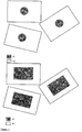
- FIG. 4 The structure of these heart / crown sheets is shown schematically figure 4 , where A1 is the CdSe and A2 is the CdS.
Landscapes
- Chemical & Material Sciences (AREA)
- Engineering & Computer Science (AREA)
- Crystallography & Structural Chemistry (AREA)
- Materials Engineering (AREA)
- Metallurgy (AREA)
- Organic Chemistry (AREA)
- Nanotechnology (AREA)
- Inorganic Chemistry (AREA)
- Condensed Matter Physics & Semiconductors (AREA)
- General Physics & Mathematics (AREA)
- Physics & Mathematics (AREA)
- Manufacturing & Machinery (AREA)
- Composite Materials (AREA)
- Liquid Deposition Of Substances Of Which Semiconductor Devices Are Composed (AREA)
- Luminescent Compositions (AREA)
- Photovoltaic Devices (AREA)
- Semiconductor Lasers (AREA)
- Inorganic Compounds Of Heavy Metals (AREA)
Claims (8)
- Kolloidales Nanosheet, umfassend einen kolloidalen halbleitenden initialen Nanokristall, lateral umgeben von einem anderen halbleitenden kristallinen Material, dargestellt von der Formel MnXy, wobei M ein Transitionsmetall ist und X ein Chalkogen; wobei der kolloidale halbleitende initiale Nanokristall und das halbleitende kristalline Metall die gleiche Dicke aufweisen; und wobei der kolloidale anorganische initiale Nanokristall und das halbleitende kristalline Metall MnXy aus CdO, CdS, CdSe, CdTe, ZnO, ZnS, ZnSe, ZnTe, PbO, PbS, PbSe, PbTe, GeS, GeSe, SnS, SnSe, GeS2, GeSe2, SnS2, SnSe2, HgS, HgSe, HgTe, CuInS2, CuInSe2, AgInS2, AgInSe2, CuS, Cu2S, Ag2S, Ag2Se, Ag2Te, FeS, FeS2, InP, Cd3P2, Zn3P2, FeO, Fe2O3, Fe3O4, Al2O3, TiO2 oder aus Legierungen davon bestehen.
- Nanosheet nach Anspruch 1, in welchem das halbleitende kristalline Material MnXy von einem Transitionsmetall dotiert ist.
- Nanosheet nach einem der vorhergehenden Ansprüche, in welchem das kolloidale Nanosheet laterale Maße über 10 nm aufweist.
- Nanosheet nach einem der vorhergehenden Ansprüche, in welchem der wenigstens eine kolloidale initiale Nanokristall ein kolloidales Nanosheet ist.
- Verwendung von kolloidalen Nanosheets nach einem der Ansprüche 1 bis 4 als großflächiges Material spezifisch für die Katalyse.
- Verwendung von kolloidalen Nanosheets nach einem der Ansprüche 1 bis 4 in einem aktiven Element einer Leuchtdiode, in einem Transistor oder in einem Laser.
- Verwendung von kolloidalen Nanosheets nach einem der Ansprüche 1 bis 4 in einem aktiven Element eines Photovoltaikmoduls, insbesondere in einem Absorber und/oder in einem Sammler von unter Lichteinwirkung erzeugten Ladungen.
- Verwendung von kolloidalen Nanosheets nach einem der Ansprüche 1 bis 4 zum Bilden von ultradünnen halbleitenden Filmen auf einem Substrat bei niedriger Temperatur.
Applications Claiming Priority (2)
| Application Number | Priority Date | Filing Date | Title |
|---|---|---|---|
| FR1004175A FR2966474B1 (fr) | 2010-10-25 | 2010-10-25 | Procede de fabrication d'un materiau nanocristallin |
| PCT/FR2011/000570 WO2012056121A1 (fr) | 2010-10-25 | 2011-10-24 | Procédé de fabrication de nanofeuillets colloïdaux par croissance latérale de nanocristaux |
Publications (2)
| Publication Number | Publication Date |
|---|---|
| EP2633102A1 EP2633102A1 (de) | 2013-09-04 |
| EP2633102B1 true EP2633102B1 (de) | 2020-09-16 |
Family
ID=44477641
Family Applications (1)
| Application Number | Title | Priority Date | Filing Date |
|---|---|---|---|
| EP11782179.3A Active EP2633102B1 (de) | 2010-10-25 | 2011-10-24 | KOLLOIDALE NANOSHEETS und deren Verwendung |
Country Status (8)
| Country | Link |
|---|---|
| US (1) | US10490624B2 (de) |
| EP (1) | EP2633102B1 (de) |
| JP (1) | JP6057903B2 (de) |
| KR (2) | KR102195665B1 (de) |
| CN (1) | CN103415655B (de) |
| ES (1) | ES2836806T3 (de) |
| FR (1) | FR2966474B1 (de) |
| WO (1) | WO2012056121A1 (de) |
Families Citing this family (27)
| Publication number | Priority date | Publication date | Assignee | Title |
|---|---|---|---|---|
| FR2981790A1 (fr) * | 2011-10-19 | 2013-04-26 | Solarwell | Procede de croissance en epaisseur de feuillets colloidaux et materiaux composes de feuillets |
| CN102797031B (zh) * | 2012-08-22 | 2015-07-08 | 兰州大学 | 一种黄铁矿型二硫化亚铁纳米单晶半导体材料的制备方法 |
| US10224258B2 (en) * | 2013-03-22 | 2019-03-05 | Applied Materials, Inc. | Method of curing thermoplastics with microwave energy |
| US9634161B2 (en) * | 2013-05-01 | 2017-04-25 | Delaware State University | Nanoscale precursors for synthesis of Fe2(Si,Ge)(S,Se)4 crystalline particles and layers |
| DE102014109501A1 (de) | 2013-11-01 | 2015-05-07 | Electronics And Telecommunications Research Institute | Vorrichtung zum Verarbeiten eines Radarsignals und Verfahren zum Verarbeiten eines Radarsignals |
| KR102309879B1 (ko) * | 2013-12-12 | 2021-10-07 | 삼성전자주식회사 | 투명 전도막 |
| US10099938B2 (en) | 2013-12-12 | 2018-10-16 | Samsung Electronics Co., Ltd. | Electrically conductive thin films |
| US9517937B2 (en) * | 2014-03-20 | 2016-12-13 | Sandia Corporation | Method to synthesize metal chalcogenide monolayer nanomaterials |
| EP3152808B1 (de) * | 2014-06-03 | 2019-08-28 | Fondazione Istituto Italiano di Tecnologia | Dauerstrich gepumpter laser mit kolloidalen nanokristallen |
| WO2017046268A1 (en) * | 2015-09-16 | 2017-03-23 | The University Of Manchester | 2d materials |
| KR102591112B1 (ko) | 2015-11-06 | 2023-10-17 | 삼성전자주식회사 | 금속 산화물 나노시트들의 집단과 그 제조 방법, 및 이를 포함하는 도전체 및 전자 소자 |
| US10062568B2 (en) * | 2016-05-13 | 2018-08-28 | Nanoco Technologies, Ltd. | Chemical vapor deposition method for fabricating two-dimensional materials |
| US20180072947A1 (en) * | 2016-09-12 | 2018-03-15 | Nanoco Technologies Ltd. | Solution-Phase Synthesis of Layered Transition Metal Dichalcogenide Nanoparticles |
| US11131031B2 (en) | 2018-06-12 | 2021-09-28 | Honda Motor Co., Ltd. | High-yield preparation of two-dimensional copper nanosheets |
| CN109748250B (zh) * | 2019-02-27 | 2022-06-28 | 深圳大学 | 一种碲硒纳米材料及其制备方法和应用 |
| US11142693B2 (en) * | 2019-04-17 | 2021-10-12 | Samsung Electronics Co., Ltd. | Nanoplatelet |
| CN110511758A (zh) * | 2019-09-19 | 2019-11-29 | 青岛大学 | 一种CdSe/CdS核壳纳米片材料及其制备方法 |
| US20230340693A1 (en) * | 2019-10-21 | 2023-10-26 | Iucf-Hyu (Industry-University Cooperation Foundation Hanyang University) | Single-crystal metal film by solid-state crystal growth of seed crystals, large-area single-layer or multilayer graphene with adjusted orientation angle using same, and method for manufacturing same |
| US12441939B2 (en) | 2019-10-31 | 2025-10-14 | Massachusetts Institute Of Technology | Light emitting nanocrystals and methods of making light emitting nanocrystals |
| US20250093561A1 (en) | 2020-02-21 | 2025-03-20 | Nexdot | Blue filters comprising semiconductor nanoparticles and uses thereof |
| CN111908434B (zh) * | 2020-07-16 | 2023-08-18 | 北京理工大学 | 一种过渡金属硫族化合物纳米片水相分散液的制备方法 |
| US12031075B2 (en) | 2020-09-02 | 2024-07-09 | The Regents Of The University Of California | Systems and methods for quantum dot on nanoplatelet heterostructures with tunable emission in the shortwave infrared |
| CN113130696B (zh) * | 2021-04-15 | 2022-07-22 | 东南大学 | 基于量子限制斯塔克效应的光开关 |
| KR102495534B1 (ko) * | 2021-07-27 | 2023-02-06 | 아주대학교산학협력단 | Cu-Fe-S 나노 결정 콜로이드를 이용한 전도성 박막 및 이의 제조방법 |
| TWI796852B (zh) * | 2021-11-29 | 2023-03-21 | 國立臺灣師範大學 | 單層二維材料的製備方法及分析方法 |
| CN116183653B (zh) * | 2021-11-29 | 2025-09-12 | 刘沂欣 | 单层二维材料的制备方法、分析方法及测量方法 |
| CN119799322A (zh) * | 2025-01-03 | 2025-04-11 | 北京师范大学珠海校区 | 一种高量子效率高稳定性硒化镉量子片及其制备方法 |
Family Cites Families (12)
| Publication number | Priority date | Publication date | Assignee | Title |
|---|---|---|---|---|
| JP4596705B2 (ja) | 2001-08-31 | 2010-12-15 | 富士フイルム株式会社 | 複合微細粒子およびその製造方法 |
| KR100612894B1 (ko) * | 2005-05-02 | 2006-08-14 | 삼성전자주식회사 | 나노와이어 소자 및 그 제조방법 |
| US8120239B2 (en) * | 2006-08-16 | 2012-02-21 | Samsung Electronics Co., Ltd. | Infrared display with luminescent quantum dots |
| KR100817853B1 (ko) | 2006-09-25 | 2008-03-31 | 재단법인서울대학교산학협력재단 | 점진적 농도구배 껍질 구조를 갖는 양자점 및 이의 제조방법 |
| EP2163301A3 (de) * | 2008-09-11 | 2010-04-28 | Centre National De La Recherche Scientifique (Cnrs) | Verfahren zur Herstellung von kolloidalen Materialien, kolloidale Materialien und ihre Verwendung |
| CN101805015B (zh) * | 2009-02-17 | 2011-12-21 | 国家纳米科学中心 | 多孔PbS纳米片的制备方法 |
| CN101519190B (zh) * | 2009-04-02 | 2010-08-25 | 北京化工大学 | 一种CdS/LDHs纳米透明复合薄膜材料的制备方法 |
| US8410455B2 (en) * | 2009-04-17 | 2013-04-02 | University Of Florida Research Foundation, Inc. | Excitation-intensity-dependent, color-tunable, dual emitting nanocrystals |
| CN101544408A (zh) * | 2009-04-17 | 2009-09-30 | 中国科学院上海硅酸盐研究所 | 水热法制备层片状Co(OH)2或Co3O4纳米棒的方法 |
| WO2011008881A2 (en) * | 2009-07-14 | 2011-01-20 | Spectrawatt, Inc. | Light conversion efficiency-enhanced solar cell fabricated with downshifting nanomaterial |
| CN101717070B (zh) | 2009-11-11 | 2012-08-15 | 中国科学院理化技术研究所 | 具有光催化功能的Al掺杂ZnO纳米片的制备方法 |
| CN101787564B (zh) * | 2010-04-01 | 2012-01-04 | 云南大学 | 一种片状ZnSe荧光纳米单晶的合成方法 |
-
2010
- 2010-10-25 FR FR1004175A patent/FR2966474B1/fr not_active Expired - Fee Related
-
2011
- 2011-10-24 EP EP11782179.3A patent/EP2633102B1/de active Active
- 2011-10-24 ES ES11782179T patent/ES2836806T3/es active Active
- 2011-10-24 WO PCT/FR2011/000570 patent/WO2012056121A1/fr not_active Ceased
- 2011-10-24 KR KR1020137010659A patent/KR102195665B1/ko not_active Expired - Fee Related
- 2011-10-24 US US13/881,450 patent/US10490624B2/en active Active
- 2011-10-24 JP JP2013534358A patent/JP6057903B2/ja not_active Expired - Fee Related
- 2011-10-24 CN CN201180058966.5A patent/CN103415655B/zh not_active Expired - Fee Related
- 2011-10-24 KR KR1020197018385A patent/KR20190078659A/ko not_active Ceased
Non-Patent Citations (1)
| Title |
|---|
| None * |
Also Published As
| Publication number | Publication date |
|---|---|
| WO2012056121A1 (fr) | 2012-05-03 |
| FR2966474A1 (fr) | 2012-04-27 |
| KR20190078659A (ko) | 2019-07-04 |
| US20130220405A1 (en) | 2013-08-29 |
| ES2836806T3 (es) | 2021-06-28 |
| FR2966474B1 (fr) | 2013-12-20 |
| CN103415655A (zh) | 2013-11-27 |
| KR20140017493A (ko) | 2014-02-11 |
| KR102195665B1 (ko) | 2020-12-28 |
| CN103415655B (zh) | 2017-04-12 |
| JP2014503444A (ja) | 2014-02-13 |
| JP6057903B2 (ja) | 2017-01-11 |
| EP2633102A1 (de) | 2013-09-04 |
| US10490624B2 (en) | 2019-11-26 |
Similar Documents
| Publication | Publication Date | Title |
|---|---|---|
| EP2633102A1 (de) | Verfahren zur herstellung von kolloidalen nanosheets mittels lateralem wachstum von nanokristallen | |
| EP2769405B1 (de) | Verfahren zur verstärkung der dicke von kolloidalen nanosheets und materialien aus diesen nanosheets | |
| Peng et al. | Selective synthesis and characterization of CdSe nanorods and fractal nanocrystals | |
| Al-Salim et al. | Synthesis of cdses nanocrystals in coordinating and noncoordinating solvents: Solvent's role in evolution of the optical and structural properties | |
| Ouyang et al. | Noninjection, one-pot synthesis of photoluminescent colloidal homogeneously alloyed CdSeS quantum dots | |
| Saunders et al. | Synthesis of high aspect ratio quantum-size CdS nanorods and their surface-dependent photoluminescence | |
| Carbone et al. | Synthesis and micrometer-scale assembly of colloidal CdSe/CdS nanorods prepared by a seeded growth approach | |
| Peng et al. | Nearly monodisperse and shape-controlled CdSe nanocrystals via alternative routes: nucleation and growth | |
| Li et al. | Size/shape-controlled synthesis of colloidal CdSe quantum disks: ligand and temperature effects | |
| Chin et al. | Highly luminescent ultranarrow Mn doped ZnSe nanowires | |
| Chu et al. | Shape-controlled synthesis of CdS nanocrystals in mixed solvents | |
| Stouwdam et al. | Photostability of colloidal PbSe and PbSe/PbS core/shell nanocrystals in solution and in the solid state | |
| Acharya et al. | An alternate route to high-quality ZnSe and Mn-doped ZnSe nanocrystals | |
| Yong et al. | Shape control of PbSe nanocrystals using noble metal seed particles | |
| EP2769404B1 (de) | Verfahren zum schichtweisen dickenwachstum von kolloidalen nanosheets und materialien aus diesen nanosheets | |
| CN100570912C (zh) | Ⅲ-ⅴ半导体核-异质壳纳米晶体 | |
| Park et al. | Aqueous phase synthesized CdSe nanoparticles with well-defined numbers of constituent atoms | |
| Wang et al. | Synthesis of tower-like ZnO structures and visible photoluminescence origins of varied-shaped ZnO nanostructures | |
| Wei et al. | Highly reactive Se precursor for the phosphine-free synthesis of metal selenide nanocrystals | |
| Yang et al. | Highly luminescent CdSe/Cd x Zn1–x S quantum dots with narrow spectrum and widely tunable wavelength | |
| Tang et al. | Synthesis and characterization of wavelength-tunable, water-soluble, and near-infrared-emitting CdHgTe nanorods | |
| Dai et al. | Ligand effects on synthesis and post-synthetic stability of PbSe nanocrystals | |
| Xi et al. | Controlling growth of CdSe nanowires through ligand optimization | |
| Trejo et al. | Synthesis and growth mechanism of one-dimensional Zn/ZnO core− shell nanostructures in low-temperature hydrothermal process | |
| Bose et al. | Anisotropic Zinc Blende ZnSe Nanostructures: The Interface Chemistry and the Retention of Zinc Blende Phase during Growth |
Legal Events
| Date | Code | Title | Description |
|---|---|---|---|
| PUAI | Public reference made under article 153(3) epc to a published international application that has entered the european phase |
Free format text: ORIGINAL CODE: 0009012 |
|
| 17P | Request for examination filed |
Effective date: 20130527 |
|
| AK | Designated contracting states |
Kind code of ref document: A1 Designated state(s): AL AT BE BG CH CY CZ DE DK EE ES FI FR GB GR HR HU IE IS IT LI LT LU LV MC MK MT NL NO PL PT RO RS SE SI SK SM TR |
|
| DAX | Request for extension of the european patent (deleted) | ||
| 17Q | First examination report despatched |
Effective date: 20140312 |
|
| RAP1 | Party data changed (applicant data changed or rights of an application transferred) |
Owner name: NEXDOT |
|
| STAA | Information on the status of an ep patent application or granted ep patent |
Free format text: STATUS: EXAMINATION IS IN PROGRESS |
|
| GRAP | Despatch of communication of intention to grant a patent |
Free format text: ORIGINAL CODE: EPIDOSNIGR1 |
|
| STAA | Information on the status of an ep patent application or granted ep patent |
Free format text: STATUS: GRANT OF PATENT IS INTENDED |
|
| RIC1 | Information provided on ipc code assigned before grant |
Ipc: C30B 29/48 20060101ALI20200207BHEP Ipc: H01L 31/0296 20060101ALI20200207BHEP Ipc: H01L 33/18 20100101ALI20200207BHEP Ipc: C30B 29/60 20060101ALI20200207BHEP Ipc: B82Y 40/00 20110101ALI20200207BHEP Ipc: H01L 31/0352 20060101ALI20200207BHEP Ipc: B82Y 30/00 20110101ALI20200207BHEP Ipc: H01L 31/032 20060101ALI20200207BHEP Ipc: C30B 7/08 20060101AFI20200207BHEP |
|
| INTG | Intention to grant announced |
Effective date: 20200227 |
|
| GRAS | Grant fee paid |
Free format text: ORIGINAL CODE: EPIDOSNIGR3 |
|
| GRAJ | Information related to disapproval of communication of intention to grant by the applicant or resumption of examination proceedings by the epo deleted |
Free format text: ORIGINAL CODE: EPIDOSDIGR1 |
|
| GRAL | Information related to payment of fee for publishing/printing deleted |
Free format text: ORIGINAL CODE: EPIDOSDIGR3 |
|
| STAA | Information on the status of an ep patent application or granted ep patent |
Free format text: STATUS: EXAMINATION IS IN PROGRESS |
|
| INTC | Intention to grant announced (deleted) | ||
| RIN1 | Information on inventor provided before grant (corrected) |
Inventor name: ITHURRIA, SANDRINE Inventor name: MAHLER, BENOIT |
|
| GRAR | Information related to intention to grant a patent recorded |
Free format text: ORIGINAL CODE: EPIDOSNIGR71 |
|
| STAA | Information on the status of an ep patent application or granted ep patent |
Free format text: STATUS: GRANT OF PATENT IS INTENDED |
|
| GRAA | (expected) grant |
Free format text: ORIGINAL CODE: 0009210 |
|
| STAA | Information on the status of an ep patent application or granted ep patent |
Free format text: STATUS: THE PATENT HAS BEEN GRANTED |
|
| INTG | Intention to grant announced |
Effective date: 20200710 |
|
| AK | Designated contracting states |
Kind code of ref document: B1 Designated state(s): AL AT BE BG CH CY CZ DE DK EE ES FI FR GB GR HR HU IE IS IT LI LT LU LV MC MK MT NL NO PL PT RO RS SE SI SK SM TR |
|
| REG | Reference to a national code |
Ref country code: GB Ref legal event code: FG4D Free format text: NOT ENGLISH |
|
| REG | Reference to a national code |
Ref country code: CH Ref legal event code: EP |
|
| REG | Reference to a national code |
Ref country code: DE Ref legal event code: R096 Ref document number: 602011068634 Country of ref document: DE |
|
| REG | Reference to a national code |
Ref country code: IE Ref legal event code: FG4D Free format text: LANGUAGE OF EP DOCUMENT: FRENCH |
|
| REG | Reference to a national code |
Ref country code: AT Ref legal event code: REF Ref document number: 1314257 Country of ref document: AT Kind code of ref document: T Effective date: 20201015 |
|
| PG25 | Lapsed in a contracting state [announced via postgrant information from national office to epo] |
Ref country code: HR Free format text: LAPSE BECAUSE OF FAILURE TO SUBMIT A TRANSLATION OF THE DESCRIPTION OR TO PAY THE FEE WITHIN THE PRESCRIBED TIME-LIMIT Effective date: 20200916 Ref country code: NO Free format text: LAPSE BECAUSE OF FAILURE TO SUBMIT A TRANSLATION OF THE DESCRIPTION OR TO PAY THE FEE WITHIN THE PRESCRIBED TIME-LIMIT Effective date: 20201216 Ref country code: BG Free format text: LAPSE BECAUSE OF FAILURE TO SUBMIT A TRANSLATION OF THE DESCRIPTION OR TO PAY THE FEE WITHIN THE PRESCRIBED TIME-LIMIT Effective date: 20201216 Ref country code: SE Free format text: LAPSE BECAUSE OF FAILURE TO SUBMIT A TRANSLATION OF THE DESCRIPTION OR TO PAY THE FEE WITHIN THE PRESCRIBED TIME-LIMIT Effective date: 20200916 Ref country code: FI Free format text: LAPSE BECAUSE OF FAILURE TO SUBMIT A TRANSLATION OF THE DESCRIPTION OR TO PAY THE FEE WITHIN THE PRESCRIBED TIME-LIMIT Effective date: 20200916 Ref country code: GR Free format text: LAPSE BECAUSE OF FAILURE TO SUBMIT A TRANSLATION OF THE DESCRIPTION OR TO PAY THE FEE WITHIN THE PRESCRIBED TIME-LIMIT Effective date: 20201217 |
|
| REG | Reference to a national code |
Ref country code: AT Ref legal event code: MK05 Ref document number: 1314257 Country of ref document: AT Kind code of ref document: T Effective date: 20200916 |
|
| REG | Reference to a national code |
Ref country code: NL Ref legal event code: MP Effective date: 20200916 |
|
| PG25 | Lapsed in a contracting state [announced via postgrant information from national office to epo] |
Ref country code: RS Free format text: LAPSE BECAUSE OF FAILURE TO SUBMIT A TRANSLATION OF THE DESCRIPTION OR TO PAY THE FEE WITHIN THE PRESCRIBED TIME-LIMIT Effective date: 20200916 Ref country code: LV Free format text: LAPSE BECAUSE OF FAILURE TO SUBMIT A TRANSLATION OF THE DESCRIPTION OR TO PAY THE FEE WITHIN THE PRESCRIBED TIME-LIMIT Effective date: 20200916 |
|
| REG | Reference to a national code |
Ref country code: LT Ref legal event code: MG4D |
|
| PG25 | Lapsed in a contracting state [announced via postgrant information from national office to epo] |
Ref country code: PT Free format text: LAPSE BECAUSE OF FAILURE TO SUBMIT A TRANSLATION OF THE DESCRIPTION OR TO PAY THE FEE WITHIN THE PRESCRIBED TIME-LIMIT Effective date: 20210118 Ref country code: NL Free format text: LAPSE BECAUSE OF FAILURE TO SUBMIT A TRANSLATION OF THE DESCRIPTION OR TO PAY THE FEE WITHIN THE PRESCRIBED TIME-LIMIT Effective date: 20200916 Ref country code: LT Free format text: LAPSE BECAUSE OF FAILURE TO SUBMIT A TRANSLATION OF THE DESCRIPTION OR TO PAY THE FEE WITHIN THE PRESCRIBED TIME-LIMIT Effective date: 20200916 Ref country code: RO Free format text: LAPSE BECAUSE OF FAILURE TO SUBMIT A TRANSLATION OF THE DESCRIPTION OR TO PAY THE FEE WITHIN THE PRESCRIBED TIME-LIMIT Effective date: 20200916 Ref country code: SM Free format text: LAPSE BECAUSE OF FAILURE TO SUBMIT A TRANSLATION OF THE DESCRIPTION OR TO PAY THE FEE WITHIN THE PRESCRIBED TIME-LIMIT Effective date: 20200916 Ref country code: EE Free format text: LAPSE BECAUSE OF FAILURE TO SUBMIT A TRANSLATION OF THE DESCRIPTION OR TO PAY THE FEE WITHIN THE PRESCRIBED TIME-LIMIT Effective date: 20200916 Ref country code: CZ Free format text: LAPSE BECAUSE OF FAILURE TO SUBMIT A TRANSLATION OF THE DESCRIPTION OR TO PAY THE FEE WITHIN THE PRESCRIBED TIME-LIMIT Effective date: 20200916 |
|
| PG25 | Lapsed in a contracting state [announced via postgrant information from national office to epo] |
Ref country code: PL Free format text: LAPSE BECAUSE OF FAILURE TO SUBMIT A TRANSLATION OF THE DESCRIPTION OR TO PAY THE FEE WITHIN THE PRESCRIBED TIME-LIMIT Effective date: 20200916 Ref country code: IS Free format text: LAPSE BECAUSE OF FAILURE TO SUBMIT A TRANSLATION OF THE DESCRIPTION OR TO PAY THE FEE WITHIN THE PRESCRIBED TIME-LIMIT Effective date: 20210116 Ref country code: AL Free format text: LAPSE BECAUSE OF FAILURE TO SUBMIT A TRANSLATION OF THE DESCRIPTION OR TO PAY THE FEE WITHIN THE PRESCRIBED TIME-LIMIT Effective date: 20200916 Ref country code: AT Free format text: LAPSE BECAUSE OF FAILURE TO SUBMIT A TRANSLATION OF THE DESCRIPTION OR TO PAY THE FEE WITHIN THE PRESCRIBED TIME-LIMIT Effective date: 20200916 |
|
| REG | Reference to a national code |
Ref country code: CH Ref legal event code: PL |
|
| REG | Reference to a national code |
Ref country code: DE Ref legal event code: R097 Ref document number: 602011068634 Country of ref document: DE |
|
| REG | Reference to a national code |
Ref country code: ES Ref legal event code: FG2A Ref document number: 2836806 Country of ref document: ES Kind code of ref document: T3 Effective date: 20210628 |
|
| PG25 | Lapsed in a contracting state [announced via postgrant information from national office to epo] |
Ref country code: SK Free format text: LAPSE BECAUSE OF FAILURE TO SUBMIT A TRANSLATION OF THE DESCRIPTION OR TO PAY THE FEE WITHIN THE PRESCRIBED TIME-LIMIT Effective date: 20200916 Ref country code: MC Free format text: LAPSE BECAUSE OF FAILURE TO SUBMIT A TRANSLATION OF THE DESCRIPTION OR TO PAY THE FEE WITHIN THE PRESCRIBED TIME-LIMIT Effective date: 20200916 Ref country code: LU Free format text: LAPSE BECAUSE OF NON-PAYMENT OF DUE FEES Effective date: 20201024 |
|
| REG | Reference to a national code |
Ref country code: BE Ref legal event code: MM Effective date: 20201031 |
|
| PLBE | No opposition filed within time limit |
Free format text: ORIGINAL CODE: 0009261 |
|
| STAA | Information on the status of an ep patent application or granted ep patent |
Free format text: STATUS: NO OPPOSITION FILED WITHIN TIME LIMIT |
|
| 26N | No opposition filed |
Effective date: 20210617 |
|
| PG25 | Lapsed in a contracting state [announced via postgrant information from national office to epo] |
Ref country code: BE Free format text: LAPSE BECAUSE OF NON-PAYMENT OF DUE FEES Effective date: 20201031 Ref country code: CH Free format text: LAPSE BECAUSE OF NON-PAYMENT OF DUE FEES Effective date: 20201031 Ref country code: DK Free format text: LAPSE BECAUSE OF FAILURE TO SUBMIT A TRANSLATION OF THE DESCRIPTION OR TO PAY THE FEE WITHIN THE PRESCRIBED TIME-LIMIT Effective date: 20200916 Ref country code: SI Free format text: LAPSE BECAUSE OF FAILURE TO SUBMIT A TRANSLATION OF THE DESCRIPTION OR TO PAY THE FEE WITHIN THE PRESCRIBED TIME-LIMIT Effective date: 20200916 Ref country code: LI Free format text: LAPSE BECAUSE OF NON-PAYMENT OF DUE FEES Effective date: 20201031 |
|
| PG25 | Lapsed in a contracting state [announced via postgrant information from national office to epo] |
Ref country code: TR Free format text: LAPSE BECAUSE OF FAILURE TO SUBMIT A TRANSLATION OF THE DESCRIPTION OR TO PAY THE FEE WITHIN THE PRESCRIBED TIME-LIMIT Effective date: 20200916 Ref country code: MT Free format text: LAPSE BECAUSE OF FAILURE TO SUBMIT A TRANSLATION OF THE DESCRIPTION OR TO PAY THE FEE WITHIN THE PRESCRIBED TIME-LIMIT Effective date: 20200916 Ref country code: CY Free format text: LAPSE BECAUSE OF FAILURE TO SUBMIT A TRANSLATION OF THE DESCRIPTION OR TO PAY THE FEE WITHIN THE PRESCRIBED TIME-LIMIT Effective date: 20200916 |
|
| PG25 | Lapsed in a contracting state [announced via postgrant information from national office to epo] |
Ref country code: MK Free format text: LAPSE BECAUSE OF FAILURE TO SUBMIT A TRANSLATION OF THE DESCRIPTION OR TO PAY THE FEE WITHIN THE PRESCRIBED TIME-LIMIT Effective date: 20200916 |
|
| P01 | Opt-out of the competence of the unified patent court (upc) registered |
Effective date: 20230509 |
|
| PGFP | Annual fee paid to national office [announced via postgrant information from national office to epo] |
Ref country code: ES Payment date: 20231227 Year of fee payment: 13 |
|
| PGFP | Annual fee paid to national office [announced via postgrant information from national office to epo] |
Ref country code: IT Payment date: 20231026 Year of fee payment: 13 Ref country code: IE Payment date: 20231023 Year of fee payment: 13 Ref country code: DE Payment date: 20231020 Year of fee payment: 13 |
|
| REG | Reference to a national code |
Ref country code: DE Ref legal event code: R119 Ref document number: 602011068634 Country of ref document: DE |
|
| PG25 | Lapsed in a contracting state [announced via postgrant information from national office to epo] |
Ref country code: DE Free format text: LAPSE BECAUSE OF NON-PAYMENT OF DUE FEES Effective date: 20250501 |
|
| PG25 | Lapsed in a contracting state [announced via postgrant information from national office to epo] |
Ref country code: IT Free format text: LAPSE BECAUSE OF NON-PAYMENT OF DUE FEES Effective date: 20241024 |
|
| PG25 | Lapsed in a contracting state [announced via postgrant information from national office to epo] |
Ref country code: IE Free format text: LAPSE BECAUSE OF NON-PAYMENT OF DUE FEES Effective date: 20241024 |
|
| REG | Reference to a national code |
Ref country code: ES Ref legal event code: FD2A Effective date: 20251203 |
|
| PGFP | Annual fee paid to national office [announced via postgrant information from national office to epo] |
Ref country code: GB Payment date: 20251022 Year of fee payment: 15 |
|
| PGFP | Annual fee paid to national office [announced via postgrant information from national office to epo] |
Ref country code: FR Payment date: 20251030 Year of fee payment: 15 |
|
| PG25 | Lapsed in a contracting state [announced via postgrant information from national office to epo] |
Ref country code: ES Free format text: LAPSE BECAUSE OF NON-PAYMENT OF DUE FEES Effective date: 20241025 |