EP2575172A2 - Halbleiterbauelement - Google Patents
Halbleiterbauelement Download PDFInfo
- Publication number
- EP2575172A2 EP2575172A2 EP20120176514 EP12176514A EP2575172A2 EP 2575172 A2 EP2575172 A2 EP 2575172A2 EP 20120176514 EP20120176514 EP 20120176514 EP 12176514 A EP12176514 A EP 12176514A EP 2575172 A2 EP2575172 A2 EP 2575172A2
- Authority
- EP
- European Patent Office
- Prior art keywords
- semiconductor chip
- region
- mosfet
- semiconductor device
- chip
- Prior art date
- Legal status (The legal status is an assumption and is not a legal conclusion. Google has not performed a legal analysis and makes no representation as to the accuracy of the status listed.)
- Withdrawn
Links
Images
















Classifications
-
- H—ELECTRICITY
- H10—SEMICONDUCTOR DEVICES; ELECTRIC SOLID-STATE DEVICES NOT OTHERWISE PROVIDED FOR
- H10D—INORGANIC ELECTRIC SEMICONDUCTOR DEVICES
- H10D84/00—Integrated devices formed in or on semiconductor substrates that comprise only semiconducting layers, e.g. on Si wafers or on GaAs-on-Si wafers
- H10D84/80—Integrated devices formed in or on semiconductor substrates that comprise only semiconducting layers, e.g. on Si wafers or on GaAs-on-Si wafers characterised by the integration of at least one component covered by groups H10D12/00 or H10D30/00, e.g. integration of IGFETs
- H10D84/82—Integrated devices formed in or on semiconductor substrates that comprise only semiconducting layers, e.g. on Si wafers or on GaAs-on-Si wafers characterised by the integration of at least one component covered by groups H10D12/00 or H10D30/00, e.g. integration of IGFETs of only field-effect components
- H10D84/83—Integrated devices formed in or on semiconductor substrates that comprise only semiconducting layers, e.g. on Si wafers or on GaAs-on-Si wafers characterised by the integration of at least one component covered by groups H10D12/00 or H10D30/00, e.g. integration of IGFETs of only field-effect components of only insulated-gate FETs [IGFET]
-
- H—ELECTRICITY
- H10—SEMICONDUCTOR DEVICES; ELECTRIC SOLID-STATE DEVICES NOT OTHERWISE PROVIDED FOR
- H10D—INORGANIC ELECTRIC SEMICONDUCTOR DEVICES
- H10D30/00—Field-effect transistors [FET]
- H10D30/60—Insulated-gate field-effect transistors [IGFET]
- H10D30/64—Double-diffused metal-oxide semiconductor [DMOS] FETs
- H10D30/66—Vertical DMOS [VDMOS] FETs
- H10D30/669—Vertical DMOS [VDMOS] FETs having voltage-sensing or current-sensing structures, e.g. emulator sections or overcurrent sensing cells
-
- H—ELECTRICITY
- H10—SEMICONDUCTOR DEVICES; ELECTRIC SOLID-STATE DEVICES NOT OTHERWISE PROVIDED FOR
- H10D—INORGANIC ELECTRIC SEMICONDUCTOR DEVICES
- H10D84/00—Integrated devices formed in or on semiconductor substrates that comprise only semiconducting layers, e.g. on Si wafers or on GaAs-on-Si wafers
- H10D84/80—Integrated devices formed in or on semiconductor substrates that comprise only semiconducting layers, e.g. on Si wafers or on GaAs-on-Si wafers characterised by the integration of at least one component covered by groups H10D12/00 or H10D30/00, e.g. integration of IGFETs
- H10D84/82—Integrated devices formed in or on semiconductor substrates that comprise only semiconducting layers, e.g. on Si wafers or on GaAs-on-Si wafers characterised by the integration of at least one component covered by groups H10D12/00 or H10D30/00, e.g. integration of IGFETs of only field-effect components
- H10D84/83—Integrated devices formed in or on semiconductor substrates that comprise only semiconducting layers, e.g. on Si wafers or on GaAs-on-Si wafers characterised by the integration of at least one component covered by groups H10D12/00 or H10D30/00, e.g. integration of IGFETs of only field-effect components of only insulated-gate FETs [IGFET]
- H10D84/83125—Integrated devices formed in or on semiconductor substrates that comprise only semiconducting layers, e.g. on Si wafers or on GaAs-on-Si wafers characterised by the integration of at least one component covered by groups H10D12/00 or H10D30/00, e.g. integration of IGFETs of only field-effect components of only insulated-gate FETs [IGFET] the IGFETs characterised by having shared source or drain regions
-
- H—ELECTRICITY
- H10—SEMICONDUCTOR DEVICES; ELECTRIC SOLID-STATE DEVICES NOT OTHERWISE PROVIDED FOR
- H10D—INORGANIC ELECTRIC SEMICONDUCTOR DEVICES
- H10D84/00—Integrated devices formed in or on semiconductor substrates that comprise only semiconducting layers, e.g. on Si wafers or on GaAs-on-Si wafers
- H10D84/80—Integrated devices formed in or on semiconductor substrates that comprise only semiconducting layers, e.g. on Si wafers or on GaAs-on-Si wafers characterised by the integration of at least one component covered by groups H10D12/00 or H10D30/00, e.g. integration of IGFETs
- H10D84/82—Integrated devices formed in or on semiconductor substrates that comprise only semiconducting layers, e.g. on Si wafers or on GaAs-on-Si wafers characterised by the integration of at least one component covered by groups H10D12/00 or H10D30/00, e.g. integration of IGFETs of only field-effect components
- H10D84/83—Integrated devices formed in or on semiconductor substrates that comprise only semiconducting layers, e.g. on Si wafers or on GaAs-on-Si wafers characterised by the integration of at least one component covered by groups H10D12/00 or H10D30/00, e.g. integration of IGFETs of only field-effect components of only insulated-gate FETs [IGFET]
- H10D84/837—Integrated devices formed in or on semiconductor substrates that comprise only semiconducting layers, e.g. on Si wafers or on GaAs-on-Si wafers characterised by the integration of at least one component covered by groups H10D12/00 or H10D30/00, e.g. integration of IGFETs of only field-effect components of only insulated-gate FETs [IGFET] comprising vertical IGFETs
- H10D84/839—Integrated devices formed in or on semiconductor substrates that comprise only semiconducting layers, e.g. on Si wafers or on GaAs-on-Si wafers characterised by the integration of at least one component covered by groups H10D12/00 or H10D30/00, e.g. integration of IGFETs of only field-effect components of only insulated-gate FETs [IGFET] comprising vertical IGFETs comprising VDMOS
-
- H—ELECTRICITY
- H10—SEMICONDUCTOR DEVICES; ELECTRIC SOLID-STATE DEVICES NOT OTHERWISE PROVIDED FOR
- H10W—GENERIC PACKAGES, INTERCONNECTIONS, CONNECTORS OR OTHER CONSTRUCTIONAL DETAILS OF DEVICES COVERED BY CLASS H10
- H10W70/00—Package substrates; Interposers; Redistribution layers [RDL]
- H10W70/40—Leadframes
- H10W70/464—Additional interconnections in combination with leadframes
- H10W70/466—Tape carriers or flat leads
-
- H—ELECTRICITY
- H10—SEMICONDUCTOR DEVICES; ELECTRIC SOLID-STATE DEVICES NOT OTHERWISE PROVIDED FOR
- H10W—GENERIC PACKAGES, INTERCONNECTIONS, CONNECTORS OR OTHER CONSTRUCTIONAL DETAILS OF DEVICES COVERED BY CLASS H10
- H10W70/00—Package substrates; Interposers; Redistribution layers [RDL]
- H10W70/40—Leadframes
- H10W70/481—Leadframes for devices being provided for in groups H10D8/00 - H10D48/00
-
- H—ELECTRICITY
- H10—SEMICONDUCTOR DEVICES; ELECTRIC SOLID-STATE DEVICES NOT OTHERWISE PROVIDED FOR
- H10W—GENERIC PACKAGES, INTERCONNECTIONS, CONNECTORS OR OTHER CONSTRUCTIONAL DETAILS OF DEVICES COVERED BY CLASS H10
- H10W90/00—Package configurations
- H10W90/811—Multiple chips on leadframes
-
- H—ELECTRICITY
- H10—SEMICONDUCTOR DEVICES; ELECTRIC SOLID-STATE DEVICES NOT OTHERWISE PROVIDED FOR
- H10W—GENERIC PACKAGES, INTERCONNECTIONS, CONNECTORS OR OTHER CONSTRUCTIONAL DETAILS OF DEVICES COVERED BY CLASS H10
- H10W72/00—Interconnections or connectors in packages
- H10W72/071—Connecting or disconnecting
- H10W72/073—Connecting or disconnecting of die-attach connectors
- H10W72/07331—Connecting techniques
- H10W72/07336—Soldering or alloying
-
- H—ELECTRICITY
- H10—SEMICONDUCTOR DEVICES; ELECTRIC SOLID-STATE DEVICES NOT OTHERWISE PROVIDED FOR
- H10W—GENERIC PACKAGES, INTERCONNECTIONS, CONNECTORS OR OTHER CONSTRUCTIONAL DETAILS OF DEVICES COVERED BY CLASS H10
- H10W72/00—Interconnections or connectors in packages
- H10W72/071—Connecting or disconnecting
- H10W72/073—Connecting or disconnecting of die-attach connectors
- H10W72/07331—Connecting techniques
- H10W72/07337—Connecting techniques using a polymer adhesive, e.g. an adhesive based on silicone or epoxy
-
- H—ELECTRICITY
- H10—SEMICONDUCTOR DEVICES; ELECTRIC SOLID-STATE DEVICES NOT OTHERWISE PROVIDED FOR
- H10W—GENERIC PACKAGES, INTERCONNECTIONS, CONNECTORS OR OTHER CONSTRUCTIONAL DETAILS OF DEVICES COVERED BY CLASS H10
- H10W72/00—Interconnections or connectors in packages
- H10W72/071—Connecting or disconnecting
- H10W72/076—Connecting or disconnecting of strap connectors
- H10W72/07631—Techniques
- H10W72/07636—Soldering or alloying
-
- H—ELECTRICITY
- H10—SEMICONDUCTOR DEVICES; ELECTRIC SOLID-STATE DEVICES NOT OTHERWISE PROVIDED FOR
- H10W—GENERIC PACKAGES, INTERCONNECTIONS, CONNECTORS OR OTHER CONSTRUCTIONAL DETAILS OF DEVICES COVERED BY CLASS H10
- H10W72/00—Interconnections or connectors in packages
- H10W72/071—Connecting or disconnecting
- H10W72/076—Connecting or disconnecting of strap connectors
- H10W72/07631—Techniques
- H10W72/07637—Techniques using a polymer adhesive, e.g. an adhesive based on silicone or epoxy
-
- H—ELECTRICITY
- H10—SEMICONDUCTOR DEVICES; ELECTRIC SOLID-STATE DEVICES NOT OTHERWISE PROVIDED FOR
- H10W—GENERIC PACKAGES, INTERCONNECTIONS, CONNECTORS OR OTHER CONSTRUCTIONAL DETAILS OF DEVICES COVERED BY CLASS H10
- H10W72/00—Interconnections or connectors in packages
- H10W72/071—Connecting or disconnecting
- H10W72/076—Connecting or disconnecting of strap connectors
- H10W72/07651—Connecting or disconnecting of strap connectors characterised by changes in properties of the strap connectors during connecting
- H10W72/07653—Connecting or disconnecting of strap connectors characterised by changes in properties of the strap connectors during connecting changes in shapes
-
- H—ELECTRICITY
- H10—SEMICONDUCTOR DEVICES; ELECTRIC SOLID-STATE DEVICES NOT OTHERWISE PROVIDED FOR
- H10W—GENERIC PACKAGES, INTERCONNECTIONS, CONNECTORS OR OTHER CONSTRUCTIONAL DETAILS OF DEVICES COVERED BY CLASS H10
- H10W72/00—Interconnections or connectors in packages
- H10W72/50—Bond wires
- H10W72/541—Dispositions of bond wires
- H10W72/5445—Dispositions of bond wires being orthogonal to a side surface of the chip, e.g. parallel arrangements
-
- H—ELECTRICITY
- H10—SEMICONDUCTOR DEVICES; ELECTRIC SOLID-STATE DEVICES NOT OTHERWISE PROVIDED FOR
- H10W—GENERIC PACKAGES, INTERCONNECTIONS, CONNECTORS OR OTHER CONSTRUCTIONAL DETAILS OF DEVICES COVERED BY CLASS H10
- H10W72/00—Interconnections or connectors in packages
- H10W72/50—Bond wires
- H10W72/551—Materials of bond wires
- H10W72/552—Materials of bond wires comprising metals or metalloids, e.g. silver
- H10W72/5522—Materials of bond wires comprising metals or metalloids, e.g. silver comprising gold [Au]
-
- H—ELECTRICITY
- H10—SEMICONDUCTOR DEVICES; ELECTRIC SOLID-STATE DEVICES NOT OTHERWISE PROVIDED FOR
- H10W—GENERIC PACKAGES, INTERCONNECTIONS, CONNECTORS OR OTHER CONSTRUCTIONAL DETAILS OF DEVICES COVERED BY CLASS H10
- H10W72/00—Interconnections or connectors in packages
- H10W72/50—Bond wires
- H10W72/551—Materials of bond wires
- H10W72/552—Materials of bond wires comprising metals or metalloids, e.g. silver
- H10W72/5524—Materials of bond wires comprising metals or metalloids, e.g. silver comprising aluminium [Al]
-
- H—ELECTRICITY
- H10—SEMICONDUCTOR DEVICES; ELECTRIC SOLID-STATE DEVICES NOT OTHERWISE PROVIDED FOR
- H10W—GENERIC PACKAGES, INTERCONNECTIONS, CONNECTORS OR OTHER CONSTRUCTIONAL DETAILS OF DEVICES COVERED BY CLASS H10
- H10W72/00—Interconnections or connectors in packages
- H10W72/50—Bond wires
- H10W72/551—Materials of bond wires
- H10W72/552—Materials of bond wires comprising metals or metalloids, e.g. silver
- H10W72/5525—Materials of bond wires comprising metals or metalloids, e.g. silver comprising copper [Cu]
-
- H—ELECTRICITY
- H10—SEMICONDUCTOR DEVICES; ELECTRIC SOLID-STATE DEVICES NOT OTHERWISE PROVIDED FOR
- H10W—GENERIC PACKAGES, INTERCONNECTIONS, CONNECTORS OR OTHER CONSTRUCTIONAL DETAILS OF DEVICES COVERED BY CLASS H10
- H10W72/00—Interconnections or connectors in packages
- H10W72/60—Strap connectors, e.g. thick copper clips for grounding of power devices
- H10W72/631—Shapes of strap connectors
-
- H—ELECTRICITY
- H10—SEMICONDUCTOR DEVICES; ELECTRIC SOLID-STATE DEVICES NOT OTHERWISE PROVIDED FOR
- H10W—GENERIC PACKAGES, INTERCONNECTIONS, CONNECTORS OR OTHER CONSTRUCTIONAL DETAILS OF DEVICES COVERED BY CLASS H10
- H10W72/00—Interconnections or connectors in packages
- H10W72/60—Strap connectors, e.g. thick copper clips for grounding of power devices
- H10W72/651—Materials of strap connectors
- H10W72/652—Materials of strap connectors comprising metals or metalloids, e.g. silver
-
- H—ELECTRICITY
- H10—SEMICONDUCTOR DEVICES; ELECTRIC SOLID-STATE DEVICES NOT OTHERWISE PROVIDED FOR
- H10W—GENERIC PACKAGES, INTERCONNECTIONS, CONNECTORS OR OTHER CONSTRUCTIONAL DETAILS OF DEVICES COVERED BY CLASS H10
- H10W72/00—Interconnections or connectors in packages
- H10W72/60—Strap connectors, e.g. thick copper clips for grounding of power devices
- H10W72/651—Materials of strap connectors
- H10W72/655—Materials of strap connectors of outermost layers of multilayered strap connectors, e.g. material of a coating
-
- H—ELECTRICITY
- H10—SEMICONDUCTOR DEVICES; ELECTRIC SOLID-STATE DEVICES NOT OTHERWISE PROVIDED FOR
- H10W—GENERIC PACKAGES, INTERCONNECTIONS, CONNECTORS OR OTHER CONSTRUCTIONAL DETAILS OF DEVICES COVERED BY CLASS H10
- H10W72/00—Interconnections or connectors in packages
- H10W72/851—Dispositions of multiple connectors or interconnections
- H10W72/853—On the same surface
- H10W72/871—Bond wires and strap connectors
-
- H—ELECTRICITY
- H10—SEMICONDUCTOR DEVICES; ELECTRIC SOLID-STATE DEVICES NOT OTHERWISE PROVIDED FOR
- H10W—GENERIC PACKAGES, INTERCONNECTIONS, CONNECTORS OR OTHER CONSTRUCTIONAL DETAILS OF DEVICES COVERED BY CLASS H10
- H10W72/00—Interconnections or connectors in packages
- H10W72/851—Dispositions of multiple connectors or interconnections
- H10W72/874—On different surfaces
- H10W72/884—Die-attach connectors and bond wires
-
- H—ELECTRICITY
- H10—SEMICONDUCTOR DEVICES; ELECTRIC SOLID-STATE DEVICES NOT OTHERWISE PROVIDED FOR
- H10W—GENERIC PACKAGES, INTERCONNECTIONS, CONNECTORS OR OTHER CONSTRUCTIONAL DETAILS OF DEVICES COVERED BY CLASS H10
- H10W72/00—Interconnections or connectors in packages
- H10W72/851—Dispositions of multiple connectors or interconnections
- H10W72/874—On different surfaces
- H10W72/886—Die-attach connectors and strap connectors
-
- H—ELECTRICITY
- H10—SEMICONDUCTOR DEVICES; ELECTRIC SOLID-STATE DEVICES NOT OTHERWISE PROVIDED FOR
- H10W—GENERIC PACKAGES, INTERCONNECTIONS, CONNECTORS OR OTHER CONSTRUCTIONAL DETAILS OF DEVICES COVERED BY CLASS H10
- H10W72/00—Interconnections or connectors in packages
- H10W72/90—Bond pads, in general
- H10W72/921—Structures or relative sizes of bond pads
- H10W72/926—Multiple bond pads having different sizes
-
- H—ELECTRICITY
- H10—SEMICONDUCTOR DEVICES; ELECTRIC SOLID-STATE DEVICES NOT OTHERWISE PROVIDED FOR
- H10W—GENERIC PACKAGES, INTERCONNECTIONS, CONNECTORS OR OTHER CONSTRUCTIONAL DETAILS OF DEVICES COVERED BY CLASS H10
- H10W72/00—Interconnections or connectors in packages
- H10W72/90—Bond pads, in general
- H10W72/931—Shapes of bond pads
- H10W72/932—Plan-view shape, i.e. in top view
-
- H—ELECTRICITY
- H10—SEMICONDUCTOR DEVICES; ELECTRIC SOLID-STATE DEVICES NOT OTHERWISE PROVIDED FOR
- H10W—GENERIC PACKAGES, INTERCONNECTIONS, CONNECTORS OR OTHER CONSTRUCTIONAL DETAILS OF DEVICES COVERED BY CLASS H10
- H10W72/00—Interconnections or connectors in packages
- H10W72/90—Bond pads, in general
- H10W72/941—Dispositions of bond pads
- H10W72/944—Dispositions of multiple bond pads
-
- H—ELECTRICITY
- H10—SEMICONDUCTOR DEVICES; ELECTRIC SOLID-STATE DEVICES NOT OTHERWISE PROVIDED FOR
- H10W—GENERIC PACKAGES, INTERCONNECTIONS, CONNECTORS OR OTHER CONSTRUCTIONAL DETAILS OF DEVICES COVERED BY CLASS H10
- H10W74/00—Encapsulations, e.g. protective coatings
-
- H—ELECTRICITY
- H10—SEMICONDUCTOR DEVICES; ELECTRIC SOLID-STATE DEVICES NOT OTHERWISE PROVIDED FOR
- H10W—GENERIC PACKAGES, INTERCONNECTIONS, CONNECTORS OR OTHER CONSTRUCTIONAL DETAILS OF DEVICES COVERED BY CLASS H10
- H10W90/00—Package configurations
- H10W90/701—Package configurations characterised by the relative positions of pads or connectors relative to package parts
- H10W90/731—Package configurations characterised by the relative positions of pads or connectors relative to package parts of die-attach connectors
- H10W90/736—Package configurations characterised by the relative positions of pads or connectors relative to package parts of die-attach connectors between a chip and a stacked lead frame, conducting package substrate or heat sink
-
- H—ELECTRICITY
- H10—SEMICONDUCTOR DEVICES; ELECTRIC SOLID-STATE DEVICES NOT OTHERWISE PROVIDED FOR
- H10W—GENERIC PACKAGES, INTERCONNECTIONS, CONNECTORS OR OTHER CONSTRUCTIONAL DETAILS OF DEVICES COVERED BY CLASS H10
- H10W90/00—Package configurations
- H10W90/701—Package configurations characterised by the relative positions of pads or connectors relative to package parts
- H10W90/751—Package configurations characterised by the relative positions of pads or connectors relative to package parts of bond wires
- H10W90/753—Package configurations characterised by the relative positions of pads or connectors relative to package parts of bond wires between laterally-adjacent chips
-
- H—ELECTRICITY
- H10—SEMICONDUCTOR DEVICES; ELECTRIC SOLID-STATE DEVICES NOT OTHERWISE PROVIDED FOR
- H10W—GENERIC PACKAGES, INTERCONNECTIONS, CONNECTORS OR OTHER CONSTRUCTIONAL DETAILS OF DEVICES COVERED BY CLASS H10
- H10W90/00—Package configurations
- H10W90/701—Package configurations characterised by the relative positions of pads or connectors relative to package parts
- H10W90/751—Package configurations characterised by the relative positions of pads or connectors relative to package parts of bond wires
- H10W90/756—Package configurations characterised by the relative positions of pads or connectors relative to package parts of bond wires between a chip and a stacked lead frame, conducting package substrate or heat sink
-
- H—ELECTRICITY
- H10—SEMICONDUCTOR DEVICES; ELECTRIC SOLID-STATE DEVICES NOT OTHERWISE PROVIDED FOR
- H10W—GENERIC PACKAGES, INTERCONNECTIONS, CONNECTORS OR OTHER CONSTRUCTIONAL DETAILS OF DEVICES COVERED BY CLASS H10
- H10W90/00—Package configurations
- H10W90/701—Package configurations characterised by the relative positions of pads or connectors relative to package parts
- H10W90/761—Package configurations characterised by the relative positions of pads or connectors relative to package parts of strap connectors
- H10W90/766—Package configurations characterised by the relative positions of pads or connectors relative to package parts of strap connectors between a chip and a stacked lead frame, conducting package substrate or heat sink
Definitions
- the present invention relates to a semiconductor device, and particularly to a technology which is effective when applied to a semiconductor device having a semiconductor chip in which a switching transistor and a current detection transistor are embedded.
- a semiconductor chip is mounted over the chip mounting portion of a lead frame, the plurality of leads of the lead frame are coupled to the plurality of electrodes of the semiconductor chip with bonding wires or the like, a sealing resin portion is formed to seal therein the chip mounting portion, the semiconductor chip, the bonding wires, and the inner lead portions of the plurality of leads, the leads are cut from the lead frame, and the outer lead portions of the leads are subjected to bending to manufacture a semiconductor device in the form of a semiconductor package.
- Patent Document 1 describes a technique related to a semiconductor device in which a main cell having a trench gate to allow a main current to flow and a current detection cell having a trench gate to allow a detection current to flow are formed over the same semiconductor substrate.
- Patent Document 2 describes a technique which provides one semiconductor chip with a high-side MOSFET and a sense MOSFET which allows a current corresponding to 1/N of a current flowing in the high-side MOSFET to flow.
- Patent Document 3 describes a technique related to a semiconductor device in which a semiconductor chip having a power transistor and a semiconductor chip having a drive circuit for driving the power transistor are included in one package.
- a power MOSFET capable of handling high power has been used as a switch element.
- a switch semiconductor package can be obtained. For example, by coupling the power MOSFET as the switch element between a power source and a load and performing ON/OFF switching of the power MOSFET, it is possible to switch between a state in which an output (voltage) from the power source is supplied to the load and a state in which the output from the power source is not supplied to the load.
- the present inventors have studied a semiconductor device manufactured by forming, in a semiconductor chip formed with the power MOSFET as the switch element, a sense MOSFET for sensing a current flowing in the power MOSFET which is smaller in area than the power MOSFET, mounting the semiconductor chip over a chip mounting portion via a conductive bonding material, and sealing them.
- the semiconductor device senses the current flowing in the power MOSFET by means of the sense MOSFET, and controls the power MOSFET in accordance with a current flowing in the sense MOSFET. For example, when it is determined that an excessive current is flowing in the power MOSFET based on the current flowing in the sense MOSFET, the power MOSFET is forcibly turned OFF to protect the semiconductor device and an electronic device using the semiconductor device.
- a crack or peel-off may occur in the conductive bonding material interposed between the semiconductor chip and the chip mounting portion.
- a current is unlikely to flow so that the region can hardly function as a current path.
- a predetermined ratio exists between the current flowing in the power MOSFET and the current flowing in the sense MOSFET.
- the ratio varies to possibly degrade accuracy in sensing the current flowing in the power MOSFET by means of the sense MOSFET. This degrades the reliability of the semiconductor device.
- a preferred aim of the present invention is to provide a technology which can improve the reliability of a semiconductor device.
- a semiconductor device is a semiconductor device in which a semiconductor chip is bonded to the upper surface of a chip mounting portion having electrical conductivity and sealed in a resin.
- the semiconductor chip is formed with a main MOSFET and a sense MOSFET for sensing a current flowing in the main MOSFET which is smaller in area than the main MOSFET.
- a conductor plate is bonded to a source pad of the main MOSFET. In a plan view, the foregoing conductor plate does not overlap a region where the sense MOSFET is formed.
- the foregoing conductor plate is bonded to the foregoing source pad so as to surround three of the sides of the region where the foregoing sense MOSFET is formed.
- the reliability of the semiconductor device can be improved.
- the components thereof are not necessarily indispensable unless particularly explicitly described otherwise or unless the components are considered to be obviously indispensable in principle.
- the shapes, positional relationships, and the like of the components and the like are referred to in the following embodiments, the shapes and the like are assumed to include those substantially proximate or similar thereto and the like unless particularly explicitly described otherwise or unless it can be considered that they obviously do not in principle. The same shall apply in regard to the foregoing numerical value and range.
- hatching may be omitted even in a cross section for improved clarity of illustration, while even a plan view may be hatched for improved clarity of illustration.
- MOSFET Metal Oxide Semiconductor Field Effect Transistor
- MOS Metal Oxide Semiconductor Field Effect Transistor
- MOSFET Metal Oxide Semiconductor Field Effect Transistor
- MOS Metal Oxide Semiconductor Field Effect Transistor
- MOSFET Metal Oxide Semiconductor Field Effect Transistor
- MOSFET Metal Oxide Semiconductor Field Effect Transistor
- MISFET Metal Insulator Semiconductor Field Effect Transistor
- FIG. 1 is a top view (plan view) of a semiconductor device PKG as the embodiment of the present invention.
- FIG. 2 is a bottom view (plan view) of the semiconductor device PKG.
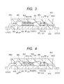
- FIGS. 3 to 6 are cross-sectional views of the semiconductor device PKG.
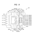
- FIGS. 7 to 9 are perspective plan views (top views) of the semiconductor device PKG.
- a cross section of the semiconductor device PKG at a position along the line A1-A1 of FIG. 7 substantially corresponds to FIG. 3 .
- a cross section of the semiconductor device PKG at a position along the line A2-A2 of FIG. 7 substantially corresponds to FIG. 4 .
- a cross section of the semiconductor device PKG at a position along the line A3-A3 of FIG. 7 substantially corresponds to FIG. 5 .
- FIG. 7 shows a perspective plan view of the top side of the semiconductor device PKG when the semiconductor device PKG is viewed through a sealing portion MR.
- FIG. 8 is a perspective plan view (top view) of the semiconductor device PKG when the semiconductor device PKG is viewed without a metal plate MPL and bonding wires BW (which are omitted) in FIG. 7 .
- FIG. 9 is a perspective plan view (top view) of the semiconductor device PKG when the semiconductor device PKG is viewed without semiconductor chips CP1 and CP2 (which are omitted) in FIG. 8 . Note that, since FIGS. 4 and 6 are cross sections each passing through a sense MOSFET region RG2 described later, the sense MOSFET region RG2 in the semiconductor chip CP1 is also shown in FIGS. 4 and 6 .
- the semiconductor chip CP1 formed with a power MOSFET (corresponding to a power MOSFET QH described later) as a switch field effect transistor, and the control semiconductor chip CP2 are integrated in one semiconductor package (packaged) to provide the one semiconductor device (semiconductor package) PKG.
- a power MOSFET corresponding to a power MOSFET QH described later
- the control semiconductor chip CP2 are integrated in one semiconductor package (packaged) to provide the one semiconductor device (semiconductor package) PKG.
- the semiconductor device PKG of the present embodiment shown in FIGS. 1 to 9 has the semiconductor chips CP1 and CP2, die pads (chip mounting portions or tabs) DP1 and DP2 for mounting the respective semiconductor chips CP1 and CP2, a plurality of leads LD each formed of a conductor, and the sealing portion MR sealing therein the foregoing members.
- the sealing portion (sealing resin portion) MR is comprised of a resin material such as, e.g., a thermosetting resin material, and can also contain a filler or the like.
- the sealing portion MR can be formed using an epoxy resin containing a filler or the like.
- the epoxy resin for the purpose of reducing a stress or the like, it may also be possible to use, e.g., a phenol curing agent, a biphenyl thermosetting resin to which silicone rubber, a filler, or the like is added as the material of the sealing portion MR.
- the sealing portion MR has an upper surface (top surface) MRa as one main surface, a lower surface (back surface or bottom surface) MRb as a main surface opposite to the upper surface MRa, and side surfaces MRc1, MRc2, MRc3, and MRc4 each intersecting the upper surface MRa and the lower surface MRb. That is, the outer appearance of the sealing portion MR is in the form of a thin plate defined by the upper surface MRa, the lower surface MRb, and the side surfaces MRc1, MRc2, MRc3, and MRc4.
- Each of the upper surface MRa and the lower surface MRb of the sealing portion MR is formed to have, e.g., a rectangular two-dimensional shape.
- the two-dimensional shape (outer shape) of the sealing portion MR which intersects the thickness thereof is a rectangle (quadrilateral).
- the side surfaces MRc1, MRc2, MRc3, and MRc4 the side surfaces MRc1 and MRc3 oppose each other and the side surfaces MRc2 and MRc4 oppose each other, while the side surface MRc1 and the side surfaces Mrc2 and MRc4 intersect each other, and the side surface MRc3 and the side surfaces Mrc2 and MRc4 intersect each other.
- the plurality of leads (lead portions) LD are each formed of a conductor, and preferably comprised of a metal material such as copper (Cu) or a copper alloy.
- Each of the plurality of leads LD has a part thereof sealed in the sealing portion MR, and another part thereof protruding from the side surface of the sealing portion MR to the outside of the sealing portion MR.
- the part of the lead LD located in the sealing portion MR will be referred to as an inner lead portion
- the part of the lead LD located outside the sealing portion MR will be referred to as an outer lead portion.
- the semiconductor device PKG of the present embodiment is a structure in which the part (outer lead portion) of each of the leads LD protrudes from the side surface of the sealing portion MR.
- the present invention is not limited thereto.
- the plurality of leads LD include a plurality of leads LD1 and a plurality of leads LD2.
- the plurality of leads LD1 included in the plurality of leads LD are disposed on the side surface MRc1 side of the sealing portion MR.
- the respective outer lead portions of the plurality of leads LD1 protrude from the side surface MRc1 of the sealing portion MR to the outside of the sealing portion MR.
- the plurality of leads LD2 included in the plurality of leads LD are disposed on the side surface MRc3 side of the sealing portion MR.
- the respective outer lead portions of the plurality of leads LD2 protrude from the side surface MRc3 of the sealing portion MR to the outside of the sealing portion MR.
- each of the leads LD (LD1 and LD2) is bent such that the lower surface of the outer lead portion located in the vicinity of the end portion thereof is located in substantially the same plane as the lower surface MRb of the sealing portion MR.
- the outer lead portion of the lead LD (LD1 or LD2) functions as the external coupling terminal portion (external terminal) of the semiconductor device PKG.
- the plurality of leads LD1 (inner lead portions thereof) disposed on the side surface MRc1 side of the sealing portion MR are coupled to each other to be integrated in the sealing portion MR.
- the die pad DP1 and the die pad DP2 are disposed adjacent to each other in a separated state with a predetermined interval kept therebetween such that one of the sides of the die pad DP1 extends along one of the sides of the die pad DP2.
- the die pad DP1 is disposed closer to the side surface MRc1 of the sealing portion MR, while the die pad DP2 is disposed closer to the side surface MRc3 of the sealing portion MR.
- the die pad DP1 is a chip mounting portion for mounting the semiconductor chip CP1, while the die pad DP2 is a chip mounting portion for mounting the semiconductor chip CP2.
- the semiconductor chip CP1 is the larger one (having a larger two-dimensional size (area)). Accordingly, of the die pads DP1 and DP2, the die pad DP1 for mounting the semiconductor chip CP1 is the larger one (having a larger two-dimensional size (area)).
- the space between the die pad DP1 and the die pad DP2 is filled with a resin material forming the sealing portion MR.
- the die pads DP1 and DP2 are electrically insulated from each other. Between the die pads DP1 and DP2, no lead LD is disposed. Along the side of the die pad DP1 (side opposite to the side thereof opposing the die pad DP2) closer to the side surface MRc1 of the sealing portion MR, the plurality of leads LD1 are disposed (arranged). Along the side of the die pad DP2 (side opposite to the side thereof opposing the die pad DP1) closer to the side surface MRc3 of the sealing portion MR, the plurality of leads LD2 are disposed (arranged).
- the plurality of leads LD1 are disposed (arranged) while, between the die pad DP2 and the side surface MRc3 of the sealing portion MR and along the side surface MRc3 of the sealing portion MR, the plurality of leads LD2 are disposed (arranged).
- the respective lower surfaces (back surfaces) of the die pads DP1 and DP2 are exposed.
- the die pads DP1 and DP2 are not exposed. Because the die pads DP1 and DP2 were coupled to a lead frame (frame body thereof) or the like when the semiconductor device PKG was manufactured, parts of the die pads DP1 and DP2 are exposed at the side surfaces MRc2 and MRc4 of the sealing portion MR.
- the die pads DP1 and DP2 are each formed of a conductor, and are preferably comprised of a metal material such as copper (Cu) or a copper alloy. More preferably, the die pads DP1 and DP2 and the plurality of leads LD each forming the semiconductor device PKG are formed of the same material (the same metal material). This allows easy production of the lead frame to which the die pads DP1 and DP2 and the plurality of leads LD are coupled, and allows easy manufacturing of the semiconductor device PKG using the lead frame.
- a metal material such as copper (Cu) or a copper alloy.
- the semiconductor chip CP1 is mounted with the top surface (main surface or upper surface) thereof facing upward and with the back surface (lower surface) thereof facing the die pad DP1.
- the semiconductor chip CP2 is mounted with the top surface (main surface or upper surface) thereof facing upward and with the back surface (lower surface) thereof facing the die pad DP2.
- the semiconductor chip CP1 (back surface thereof) is adhesively bonded and fixed to the die pad DP1 (upper surface thereof) via an adhesive layer (bonding material) BD1.
- the semiconductor chip CP2 (back surface thereof) is adhesively bonded and fixed to the die pad DP2 (upper surface thereof) via an adhesive layer (bonding material) BD2.
- the semiconductor chips CP1 and CP2 are sealed in the sealing portion MR, and are not exposed from the sealing portion MR.
- the semiconductor chip CP1 has a back-side electrode BE formed over the back surface (main surface to be adhesively bonded to the die pad DP1) thereof. Accordingly, the adhesive layer BD1 for adhesively bonding the semiconductor chip CP1 has electrical conductivity and, via the conductive adhesive layer BD1, the back-side electrode BE of the semiconductor chip CP1 is bonded and fixed to the die pad DP1, and is also electrically coupled thereto.
- the back-side electrode BE of the semiconductor chip CP1 is electrically coupled to the drain of the power MOSFET (corresponding to the power MOSFET QH described later) formed in the semiconductor chip CP1.
- the adhesive layer BD1 is comprised of a conductive paste-type adhesive such as, e.g., a silver (Ag) paste, a solder, or the like.
- the semiconductor chip CP2 does not have a back-side electrode formed over the back surface thereof. Accordingly, the adhesive layer BD2 for adhesively bonding the semiconductor chip CP2 may be either electrically conductive or insulating. If the adhesive layer BD2 is formed of the same material as that of the adhesive layer BD1, the steps of assembling the semiconductor device PKG can be simplified.
- the semiconductor chips CP1 and CP2 are manufactured by forming various semiconductor elements or semiconductor integrated circuits in a main surface of a semiconductor substrate (semiconductor wafer) comprised of, e.g., single-crystal silicon or the like, and then dividing the semiconductor substrate into individual semiconductor chips by dicing or the like.
- a semiconductor substrate semiconductor wafer
- Each of the semiconductor chips CP1 and CP2 has a rectangular (quadrilateral) two-dimensional shape intersecting the thickness thereof.
- the semiconductor chip CP1 has a two-dimensional area larger than that of the semiconductor chip CP2, and the following is a reason for the different two-dimensional areas. That is, the semiconductor chip CP2 is formed with a control circuit for controlling the gate of the semiconductor chip CP1 and the like.
- the semiconductor chip CP1 is formed with the power MOSFET (corresponding to the power MOSFET QH described later). In the power MOSFET, an ON resistance produced in the transistor is desired to be minimized. A reduced ON resistance can be achieved by increasing a channel width per unit transistor cell area. For this reason, the semiconductor chip CP1 is formed to have an outer size larger than that of the semiconductor chip CP2.
- a plurality of pad electrodes (pads, bonding pads, or terminals) PD are formed.
- the "pad electrodes” may also be simply referred to as "pads”.
- the types of the pad electrodes PD of the semiconductor chip CP1 they will be described later.
- a plurality of pad electrodes (pads, bonding pads, or terminals) PD2 are formed.
- the main surface over which the plurality of pad electrodes PD are formed will be referred to as the top surface of the semiconductor chip CP1, and the main surface opposite to the top surface and opposing the die pad DP1 will be referred to as the back surface of the semiconductor chip CP1.
- the main surface over which the plurality of pad electrodes PD2 are formed will be referred to as the top surface of the semiconductor chip CP2, and the main surface opposite to the top surface and opposing the die pad DP2 will be referred to as the back surface of the semiconductor chip CP2.
- the top surface of the semiconductor chip CP2 has a rectangular two-dimensional shape having two long sides and two short sides shorter than the two long sides.
- the plurality of pad electrodes PD2 are disposed over the top surface of the semiconductor chip CP2 and along the two long sides. Of the two long sides of the semiconductor chip CP2, one long side opposes the semiconductor chip CP1, and the other long side opposes the plurality of leads LD2.
- the plurality of pad electrodes PD of the semiconductor chip CP1 include a pad electrode (bonding pad) PDS1 having a large area. Each of the pad electrodes PD other than the pad electrode PDS1 has an area smaller than that of the pad electrode PDS1.
- the pad electrode PDS1 is a source pad electrode (bonding pad), and is electrically coupled to the source (source S1 described later) of the power MOSFET (corresponding to the power MOSFET QH described later) formed in the semiconductor chip CP1.
- the top surface of the semiconductor chip CP1 has a rectangular two-dimensional shape having sides (chip sides) SD1, SD2, SD3, and SD4. Over the top surface of the semiconductor chip CP1 and along the side SD1 opposing the semiconductor chip CP2, the pad electrodes PD other than the pad electrode PDS1 are disposed.
- the side SD3 of the semiconductor chip CP1 (here, the side SD3 of the semiconductor chip CP1 opposes the foregoing side SD1) opposes the plurality of leads LD1.
- the sides SD1 and SD3 oppose each other, the sides SD2 and SD4 oppose each other, the sides SD1 and SD3 are parallel with each other, the sides SD2 and SD4 are parallel with each other, the side SD1 is orthogonal to the sides SD2 and SD4, and the side SD3 is orthogonal to the sides SD2 and SD4.
- the plurality of pads PD of the semiconductor chip CP1 other than the pad electrode PDS1 are electrically coupled to the plurality of pads PD2 of the semiconductor chip CP2 via the plurality of bonding wires BW each as a conductive coupling member.
- the plurality of leads LD2 (inner lead portions thereof) are electrically coupled to the plurality of pad electrodes PD2 of the semiconductor chip CP2 via the plurality of bonding wires BW each as the conductive coupling member.
- the bonding wires BW are the conductive coupling members, and are more specifically conductive wires.
- the bonding wires BW are comprised of metal thin wires such as gold (Au) wires, copper (Cu) wires, or aluminum (A1) wires.
- the bonding wires BW are sealed in the sealing portion MR, and are not exposed from the sealing portion MR.
- the plurality of pad electrodes PD2 of the semiconductor chip CP2 those disposed over the top surface of the semiconductor chip CP2 and along a side SD5 thereof opposing the semiconductor chip CP1 are electrically coupled to those of the plurality of pad electrodes PD of the semiconductor chip CP1 other than the pad electrode PDS1 via the bonding wires BW.
- those disposed over the top surface of the semiconductor chip CP and along a side SD6 thereof opposing the plurality of leads LD2 are electrically coupled to the plurality of leads LD2 (inner lead portions thereof) via the bonding wires BW.
- one end portion is coupled to the pad electrode PD2 of the semiconductor chip CP2, and the other end portion is coupled to the pad electrode PD of the semiconductor chip CP1 or the inner lead portion of the lead LD2.
- the spaces between the inner lead portions of the adjacent leads LD2 and between the inner lead portions of the leads LD2 and the die pad DP2 are filled with the material forming the sealing portion MR.
- the pad electrode PDS1 of the semiconductor chip CP1 is electrically coupled to the leads LD1 via the metal plate MPL. That is, of the pad electrodes PD and PD2 of the semiconductor chips CP1 and CP2, the pad electrode PDS1 is not coupled to the bonding wire BW, but is coupled to the metal plate MPL, and the pad electrodes PD and PD2 other than the pad electrode PDS1 are coupled to the bonding wires BW.
- the metal plate MPL is sealed in the sealing portion MR, and is not exposed from the sealing portion MR.
- one end portion of the metal plate MPL is bonded to the pad electrode PDS1 of the semiconductor chip CP1 via the conductive adhesive layer (bonding material) BD3 to be electrically coupled thereto, while the other end portion of the metal plate MPL is bonded to the leads LD1 (inner lead portions thereof) via the conductive adhesive layer (bonding material) BD4 to be electrically coupled thereto.
- the adhesive layers (bonding materials) BD3 and BD4 used to bond the metal plate MPL are each required to have electrical conductivity, and a conductive paste-type adhesive material such as, e.g., a silver paste, a solder, or the like can be used. If the adhesive layers (bonding materials) BD3 and BD4 are each formed of the same material, the steps of assembling the semiconductor device PKG can be simplified.
- the metal plate MPL is formed of a metal (metal material) having a high electrical conductivity and a high thermal conductivity such as, e.g., copper (Cu), a copper (Cu) alloy, aluminum (A1), or an aluminum (A1) alloy.
- the metal plate MPL is formed of copper (Cu) or a copper (Cu) alloy in terms of its excellent workability, high thermal conductivity, and relatively low price.
- the width of the metal plate MPL is larger (wider) than the width (diameter) of each of the bonding wires BW.
- the source pad electrode PDS1 of the semiconductor chip CP1 is electrically coupled to the lead LD1 through the metal plate MPL, compared to the case where the source pad electrode PDS1 of the semiconductor chip CP1 is coupled to the lead LD1 with a wire, the ON resistance of a power MOSFET (corresponding to the power MOSFET QH described later) formed in the semiconductor chip CP1 can be reduced. This allows a reduction in package resistance and a reduction in conduction loss. Moreover, by using the metal plate MPL formed of a metal material less costly than gold instead of a wire formed of gold (Au), the cost of the semiconductor device PKG can be reduced.
- openings OP are provided to allow the state and amount of the adhesive layer BD3 bonding the metal plate MPL to the pad electrode PDS1 of the semiconductor chip CP1 to be observed through the openings OP or reduce a stress produced in each of the metal plates MPL during manufacturing steps (assembling steps) of the semiconductor device PKG.
- the plurality of leads LD1 are disposed.
- the inner lead portions of the plurality of leads LD1 are integrally coupled to each other in the sealing portion MR, and the metal plate MPL is coupled (bonded) thereto via the foregoing adhesive layer BD4.
- the five leads LD1 are disposed over the side surface MRc1 of the sealing portion MR.
- the inner lead portions of the five leads LD1 are integrally coupled to each other in the sealing portion MR, and the metal plate MPL is coupled (bonded) thereto via the foregoing adhesive layer BD4.
- the inner lead portions of the plurality of leads LD1 are coupled to each other because each of the plurality of leads LD1 is used as a terminal electrically coupled to the source pad PDS1 of the semiconductor chip CP1, i.e., as a terminal electrically coupled to the source of the power MOSFET QH formed in the semiconductor chip CP1, which will be described later.
- the volume can be increased to be larger than in the case where the plurality of leads LD1 are separately provided. This allows a reduction in package resistance and a reduction in conduction loss.
- the spaces between the inner lead portions of the leads LD1 and the die pad DP1 are filled with the material forming the sealing portion MR so that they are electrically insulated from each other.
- the inner lead portions of the plurality of leads LD1 can also be separately provided instead of being coupled to each other.
- the metal plate MPL may be coupled (bonded) appropriately to the plurality of inner lead portions (inner lead portions of the leads LD1) separately provided.
- the respective lower surfaces (back surfaces) of the die pads DP1 and DP2 are exposed from the lower surface MRb of the sealing portion MR.
- the heat generated during the operation of the semiconductor chips CP1 and CP2 is radiated mainly from the back surfaces of the semiconductor chips CP1 and CP2 through the die pads DP1 and DP2 to the outside. Therefore, the die pads DP1 and DP2 are formed to have respective areas larger than those of the semiconductor chips CP1 and CP2 mounted thereover. This allows an improvement in heat radiation property.
- the semiconductor chip CP1 generates a larger amount of heat.
- the die pad DP1 for mounting the semiconductor chip CP1 such that the two-dimensional area thereof is larger than the two-dimensional area of the die pad DP2 for mounting the semiconductor chip CP2, it is possible to efficiently release heat generated from the semiconductor chip CP1 to allow a further improvement in heat radiation property.
- FIG. 10 is a perspective plan view (top view) showing a modification of the semiconductor device PKG of the present embodiment, which corresponds to FIG. 9 described above. Similarly to FIG. 9 described above, FIG. 10 also shows a perspective plan view of the top side of the semiconductor device PKG when the semiconductor device PKG is viewed through the sealing portion MR without the metal MPL, the bonding wires BW, and the semiconductor chips CP1 and CP2.
- the die pads DP1 and DP2 are formed with respective openings OP1.
- Each of the openings OP1 is filled with the material forming the sealing portion MR.
- a lead frame to which the die pads DP1 and DP2 and the plurality of leads LD are coupled can be used and, in this case, to stably couple the die pads DP1 and DP2 to the frame body of the lead frame, a suspension lead TL can also be added.
- the suspension lead TL the portions protruding from the sealing portion MR after the formation of the sealing portion MR are cut away and removed, while the suspension lead TL in the sealing portion MR remains therein.
- FIG. 10 shows the suspension lead TL remaining in the sealing portion MR.
- the configuration of the semiconductor device PKG of the modification shown in FIG. 10 is otherwise the same as the semiconductor device PKG of FIGS. 1 to 9 described above so that a description thereof is omitted herein.
- FIG. 11 is a cross-sectional view showing an example of the mounting of the semiconductor device PKG.
- FIG. 11 shows a cross section corresponding to FIG. 3 described above.
- a plurality of terminals TML are formed in the upper surface of a mounting substrate (wiring substrate) PWB for mounting the semiconductor device PKG.
- a conductive bonding material such as a solder SL to be electrically coupled thereto.
- the respective lower surfaces of the die pads DP1 and DP2 exposed at the lower surface MRb of the sealing portion MR of the semiconductor device PKG are also bonded to the terminals TML in the upper surface of the mounting substrate PWB via a conductive bonding material such as the solder SL to be electrically coupled thereto.
- the lower surface of the die pad DP2 having the semiconductor chip CP2 mounted thereover need not be coupled to the terminal TML of the mounting substrate PWB but, in the case where the lower surface of the die pad DP2 is coupled to the terminal TML of the mounting substrate PWB, heat generated from the semiconductor chip CP2 can be released to the mounting substrate PWB via the die pad DP2.
- terminals TML1 to be coupled to the back-side electrode BE of the semiconductor chip CP1 which are among the plurality of terminals TML of the mounting substrate PWB, are coupled to the die pad DP1 (lower surface thereof) exposed at the lower surface MRb of the sealing portion MR via a conductive bonding material such as the solder SL.
- This allows the plurality of terminals TML1 of the mounting substrate PWB to be electrically coupled to the back-side electrode BE of the semiconductor chip CP1 through the die pad DP1.
- This also allows heat generated from the semiconductor chip CP1 to be released to the mounting substrate PWB through the die pad DP1.
- the outer lead portions of the individual leads LD (LD1 and LD2) and the die pad DP1 exposed at the lower surface MRb of the sealing portion MR are allowed to function as the external coupling terminal portions (external terminals) of the semiconductor device PKG.
- the lead frame to which the foregoing die pads DP1 and DP2 and the plurality of leads LD are integrally coupled is prepared first, and then a die bonding step is performed to mount the semiconductor chips CP1 and CP2 over the foregoing die pads PD1 and PD2 of the lead frame via the bonding material (which will serve as the foregoing adhesive layers BD1 and BD2) and bond the semiconductor chips CP1 and CP2 thereto.
- the bonding material which will serve as the foregoing adhesive layers BD1 and BD2
- a wire bonding step is performed to provide coupling between the pad electrodes PD of the semiconductor chip CP1 and the pad electrodes PD2 of the semiconductor chip CP2 and between the pad electrodes PD2 of the semiconductor chip CP2 and the foregoing leads LD2 via the foregoing bonding wires BW.
- coupling is provided between the source pad electrode PDS1 of the semiconductor chip CP1 and the foregoing leads LD1 via the foregoing metal plate MPL.
- a mold step is performed to form the foregoing sealing portion MR. Then, by cutting (disconnecting) the foregoing die pads DP1 and DP2 and the leads LD from the lead frame and bending the outer lead portions of the leads LD, the semiconductor device PKG can be manufactured.
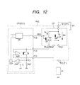
- FIG. 12 is a circuit diagram (circuit block diagram) of the semiconductor device PKG.
- the portion enclosed by the dotted line is formed of the semiconductor chip CP1
- the portion enclosed by the dot-dash line is formed of the semiconductor chip CP2
- the portion enclosed by the two-dot dash line is formed of the semiconductor device PKG.
- the semiconductor device PKG has one switch power MOSFET (Metal Oxide Semiconductor Field Effect Transistor) QH, a sense MOSFET QS for sensing a current flowing in the power MOSFET QH, and a control circuit CLC.
- the control circuit CLC is formed in the foregoing semiconductor chip CP2.
- the power MOSFET QH and the sense MOSFET QS are formed in the semiconductor chip CP1.
- the control circuit CLC has a driver circuit (drive circuit) DR as a drive circuit.
- the driver circuit DR controls a potential at the gate terminal of the power MOSFET QH in response to a Pulse Width Modulation (PWM) signal supplied from (a control circuit) outside the semiconductor device PKG or the like to control the operation of the power MOSFET QH.
- PWM Pulse Width Modulation
- a circuit for generating the pulse width modulation (PWM) signal can also be provided in the control circuit CLC.
- the output of the driver circuit DR is electrically coupled to the gate terminal of the power MOSFET QH.
- the driver circuit DR can be regarded as the driver circuit (drive circuit) of the power MOSFET QH.
- the gate of the power MOSFET QH is coupled to the driver circuit DR.
- an ON signal gate voltage for bringing the power MOSFET QH into an ON state
- the power MOSFET QH can be brought into the ON state.
- the power MOSFET QH When the power MOSFET QH is brought into the ON state by supplying the ON signal from the driver circuit DR to the gate of the power MOSFET QH, the voltage of a power source BT is outputted from the power MOSFET QH to a load LA.
- the power MOSFET QH When the power MOSFET QH is brought into an OFF state by supplying an OFF signal from the driver circuit DR to the gate of the power MOSFET QH (or stopping the supply of the ON signal), the supply of the voltage from the power source BT to the load LA is stopped.
- Such ON/OFF control of the power MOSFET QH of the semiconductor chip CP1 is performed by the control circuit CLC (driver circuit DR) of the semiconductor chip CP2.
- the semiconductor device PKG can function as a switch semiconductor device which performs ON/OFF switching of the application of the voltage from the power source BT to the load LA.
- the power MOSFET QH of the semiconductor chip CP1 can function as a switch element (switching element). Since the output of the power MOSFET QH is supplied to the load LA, the power MOSFET QH can also be regarded as an output circuit.
- the load LA any electronic device (or electronic component) desired to be coupled to the power source BT via the switch semiconductor device PKG can be used appropriately.
- the sense MOSFET QS for current sensing is provided in the semiconductor chip CP1 of the semiconductor device PKG.
- the current flowing in the power MOSFET QH is sensed by the sense MOSFET QS and, in accordance with a current flowing in the sense MOSFET QS, the power MOSFET QH is controlled.
- the gate voltage of the power MOSFET QH is controlled to limit the current of the power MOSFET QH to a value of not more than the prescribed value or the power MOSFET QH is forcibly turned OFF to allow the semiconductor device PKG and an electronic device using the semiconductor device PKG to be protected.
- the sense MOSFET QS has a drain and a gate which are common to those of the power MOSFET QH. That is, the drain of the power MOSFET QH and the drain of the sense MOSFET QS are electrically coupled to the foregoing back-side electrode BE of the semiconductor chip CP1, and therefore electrically coupled to each other. Accordingly, the foregoing back-side electrode BE of the semiconductor chip CP1 is the drain back-side electrode of each of the power MOSFET QH and the sense MOSFET QS.
- the drain (common drain) of the power MOSFET QH and the sense MOSFET QS is coupled to the terminal TE1 (the foregoing die pad DP1 corresponds to the terminal TE1) such that the same potential is supplied to the drain of the sense MOSFET QS and to the drain of the power MOSFET QH.
- the terminal TE1 is coupled to the power source (battery) BT disposed outside the semiconductor device PKG.
- the gate of the sense MOSFET QS and the gate of the power MOSFET QH are electrically coupled to each other to provide a common gate.
- the common gate is coupled to the driver circuit DR such that the same gate signal (gate voltage) is inputted from the driver circuit DR to the gate of the sense MOSFET QS and to the gate of the power MOSFET QH.
- the source of the sense MOSFET QS is not common to the source of the power MOSFET QH, and there is no short circuit between the source of the power MOSFET QH and the source of the sense MOSFET QS.
- the source of the power MOSFET QH is coupled to a terminal TE2 (the foregoing lead LD1 corresponds to the terminal TE2).
- the load LA disposed outside the semiconductor device PKG is coupled. That is, the source of the power MOSFET QH is coupled to the load LA.
- the source of the sense MOSFET QS is coupled to the control circuit CLC.
- the source of the sense MOSFET QS is coupled to the source of a transistor (p-channel MOSFET) TR formed in the control circuit CLC, and the drain of the transistor TR is coupled to a comparator circuit CMP and a resistor (reference resistor) RST. Note that, in FIG.
- the mark D1 denotes the drain of the power MOSFET QH
- the mark S1 denotes the source of the power MOSFET QH
- the mark D2 denotes the drain of the sense MOSFET QS
- the mark S2 denotes the source of the sense MOSFET QS.
- the sense MOSFET QS is formed together with the power MOSFET QH in the semiconductor chip CP1.
- the sense MOSFET QS is formed so as to configure, in conjunction with the power MOSFET QH, a current mirror circuit in the semiconductor chip CP1.
- the sense MOSFET QS has a size corresponding to 1/20000 of the size of the power MOSFET QH.
- the size ratio therebetween can be changed as necessary, but, here, a description will be given below on the assumption that the size ratio is 1/20000.
- the control circuit DLC has an amplifier circuit AMP and the transistor TR. To the two input nodes of the amplifier circuit AMP, the source of the power MOSFET QH and the source of the sense MOSFET QS are coupled. By the output node of the amplifier circuit AMP, the gate of the transistor TR is driven.
- the sense MOSFET QS is an element for detecting a current Idh flowing in the power MOSFET QH. In the sense MOSFET QS, a current corresponding to a predetermined proportion (which is 1/20000 here) of the current Idh flows due to the current mirror configuration described above when the source voltage of the sense MOSFET QS is equal to that of the power MOSFET QH.
- the amplifier circuit AMP and the transistor TR are provided.
- the drain of the transistor TR is coupled to the resistor RST.
- the resistor RST is a resistive element for current-voltage conversion. Specifically, one end of the resistor RST is coupled the drain of the transistor TR, while the other end of the resistor RST is coupled to a ground potential (0 V).
- the value of the current flowing in the sense MOSFET QS can be converted to the value of a voltage at a terminal TE3 (as the current Ise flowing in the sense MOSFET QS increases, the voltage value at the terminal TE3 increases and, specifically, the voltage value at the terminal TE3 is substantially proportional to the current Ise flowing in the sense MOSFET QS).
- the terminal TE3 is located between the drain of the transistor TR and the resistor RST.
- the drain of the transistor TR is coupled to the terminal TE3, and the terminal TE3 is coupled to one end of the resistor RST (the other end of the resistor RST is coupled to the ground potential).
- the resistor RST can be formed in the control circuit CLC (i.e., in the semiconductor chip CP2). However, in another form, it is also possible to provide the resistor RST outside the semiconductor chip CP2 (i.e., outside the semiconductor device PKG) (i.e., to provide the resistor RST as an external resistor).
- the voltage at the terminal TE3 is compared to a predetermined comparison voltage V 1 by the comparator circuit CMP in the control circuit CLC.
- an overcurrent protection circuit OCP in the control circuit CLC operates to control the driver circuit DR and bring the power MOSFET QH into the OFF state (i.e., turn OFF the gate signal inputted to the gate of the power MOSFET QH).
- the current in the power MOSFET QH is reduced to be not more than a predetermined value (i.e., the gate voltage inputted to the gate of the power MOSFET QH is reduced).
- the current Idh flowing in the power MOSFET QH is sensed (as the current Ise flowing in the sense MOSFET QS) by means of the sense MOSFET QS.
- the control circuit CLC turns OFF (OFF state or non-conductive state) the power MOSFET QH or reduces the current in the power MOSFET QH. In this manner, when an excessive current flows in the power MOSFET QH, it is possible to forcibly turn OFF the power MOSFET QH or reduce the current in the power MOSFET QH.
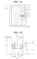
- FIGS. 13 to 15 are plan views showing the chip layout of the semiconductor chip CP1.
- FIG. 16 is a partially enlarged plan view (main-portion plan view) of the semiconductor chip CP1.
- FIGS. 17 to 19 are main-portion cross-sectional views of the semiconductor chip CP1.
- FIG. 13 corresponds to the top view of the semiconductor chip CP1, and shows the top surface side (i.e., main surface having the pad electrodes PD formed thereover) of the semiconductor chip CP1.
- FIG. 13 is a plan view but, for easier understanding, the bonding pads (pad electrodes PD including the pad electrodes PDG, PDS1, PDS2, PDS3, and PDS4) are hatched therein.
- the bonding pads pad electrodes PD including the pad electrodes PDG, PDS1, PDS2, PDS3, and PDS4 are hatched therein.
- FIG. 14 is a plan view, but shows the main MOSFET region RG1 and the sense MOSFET region RG2 in the semiconductor chip CP1 by hatching, and shows the positions of the bonding pads (pad electrodes PD including the pad electrodes PDG, PDS1, PDS2, PDS3, and PDS4) by the dotted lines.
- FIG. 14 is a plan view, but shows the main MOSFET region RG1 and the sense MOSFET region RG2 in the semiconductor chip CP1 by hatching, and shows the positions of the bonding pads (pad electrodes PD including the pad electrodes PDG, PDS1, PDS2, PDS3, and PDS4) by the dotted lines.
- FIG. 15 is a plan view, but shows the layout of source wires 10S1 and 10S2 in the semiconductor chip CP1 by the hatched regions, and shows the positions of the bonding pads (pad electrodes PD including the pad electrodes PDG, PDS1, PDS2, PDS3, and PDS4) by the dotted lines. Note that the positions of the bonding pads (pad electrodes PD including the pad electrodes PDG, PDS1, PDS2, PDS3, and PDS4) shown by the dotted lines in FIGS. 14 and 15 correspond to the regions shown by hatching in FIG. 13 .
- FIG. 16 is a partially enlarged plan view obtained by enlarging a region 20 enclosed by the two-dot-dash line in FIG.
- FIG. 13 shows the layout of the main MOSFET region RG1, the sense MOSFET region RG2, the pad electrodes PDS1 and PDS4, and the source wires 10S1 and 10S2.
- the portion (range) denoted by the mark RG1 corresponds to the main-portion cross-sectional view of the main MOSFET region RG1.
- the portion (range) denoted by the mark RG2 corresponds to the main-portion cross-sectional view of the sense MOSFET region RG2.
- FIG. 19 substantially corresponds to a cross-sectional view along the line B1-B1 of FIG. 16 .
- the substrate 1 has a substrate main body (semiconductor substrate or semiconductor wafer) 1a comprised of, e.g., n + -type single-crystal silicon into which arsenic (As) has been introduced or the like, and an epitaxial layer (semiconductor layer) 1b comprised of, e.g., n - -type single-crystal silicon and formed over the main surface of the substrate main body 1a. Accordingly, the substrate 1 is a so-called epitaxial wafer.
- a field insulating film (isolation region) 2 comprised of, e.g., a silicon oxide or the like is formed.
- the field insulating film 2 is formed of an insulator such as a silicon oxide, and can function as the isolation region for delimiting (defining) active regions.
- a plurality of unit transistor cells forming the power MOSFET QH are formed in the main MOSFET region RG1, in the active region surrounded by the field insulating film 2 and a p-type well PWL in a layer located thereunder.
- the power MOSFET QH is formed of the plurality of unit transistor cells provided in the main MOSFET region RG1 and coupled in parallel to each other.
- the sense MOSFET region RG2 in the active region surrounded by the field insulating film 2 and the p-type well PWL in the layer located thereunder, a plurality of unit transistor cells forming the sense MOSFET QS are formed in the sense MOSFET QS.
- the sense MOSFET QS is formed of the plurality of unit transistor cells provided in the sense MOSFET region RG2 and coupled in parallel to each other.
- the individual unit transistor cells formed in the main MOSFET region RG1 and the individual unit transistor cells formed in the sense MOSFET region RG2 have basically the same structures (configurations).
- the main MOSFET region RG1 is different in area from the sense MOSFET region RG2, and the area of the main MOSFET region RG1 is larger than that of the sense MOSFET region RG2. In other words, the area of the sense MOSFET region RG2 is smaller than that of the main MOSFET region RG1.
- the number of the coupled unit transistor cells in the power MOSFET QH is different from the number of the coupled unit transistor cells in the sense MOSFET QS.
- the number of the unit transistor cells forming the sense MOSFET QS and coupled in parallel to each other is smaller than the number of the unit transistor cells forming the power MOSFET QH and coupled in parallel to each other.
- a current smaller than the current flowing in the power MOSFET QH flows.
- Each of the unit transistor cells in the main MOSFET region RG1 and the sense MOSFET region RG2 is formed of, e.g., an n-channel MOSFET having a trench gate structure.
- the foregoing substrate main body 1a and the epitaxial layer 1b have the function of the drain region of each of the foregoing unit transistor cells.
- the drain back-side electrode (back-side drain electrode or drain electrode) BE is formed over the back surface (entire back surface) of the substrate 1 (semiconductor chip CP1).
- the back-side electrode BE is formed by successively stacking, e.g., a titanium (Ti) layer, a nickel (Ni) layer, and a gold (Au) layer in an ascending order from the back surface of the substrate 1.
- the back-side electrode BE of the semiconductor chip CP1 is bonded to the foregoing die pad DP1 via the foregoing adhesive layer BD1 to be electrically coupled thereto.
- a p-type semiconductor region 3 formed in the epitaxial layer 1b has the function of the channel formation region of each of the foregoing unit transistor cells.
- an n + -type semiconductor region 4 formed over the p-type semiconductor region 3 has the function of the source region of each of the foregoing unit transistor cells. Accordingly, the semiconductor region 4 is a source semiconductor region.
- trenches 5 are formed in the substrate 1 to extend from the main surface thereof in the thickness direction of the substrate 1.
- the trenches 5 are formed to extend from the upper surface of the n + -type semiconductor region 4 through the n + -type semiconductor region 4 and the p-type semiconductor region 3 and terminate in the epitaxial layer 1b in a layer located thereunder.
- gate insulating films 6 each comprised of a silicon oxide or the like are formed.
- gate electrodes 7 are embedded via the foregoing gate insulating films 6.
- the gate electrodes 7 are each comprised of a polysilicon film into which, e.g., an n-type impurity (e.g., phosphorus) has been introduced. Each of the gate electrodes 7 has the function of the gate electrode of each of the foregoing unit transistor cells.
- an n-type impurity e.g., phosphorus
- wiring portions 7a for gate extraction each comprised of a conductive film in the same layer as those of the gate electrodes 7 are formed.
- the gate electrodes 7 and the wiring portions 7a for gate extraction are integrally formed and electrically coupled to each other.
- Each of the wiring portions 7a for gate extraction is electrically coupled to a gate wire 10G through a contact hole (opening or through hole) 9a formed in an insulating film 8 covering the wiring portions 7a for gate extraction.
- the gate wire 10G is electrically coupled to the plurality of gate electrodes 7 formed in the main MOSFET region RG1 through the wiring portions 7a for gate extraction, and also electrically coupled to the plurality of gate electrodes 7 formed in the sense MOSFET region RG2 through the wiring portions 7a for gate extraction. Accordingly, the gate wire 10G is electrically coupled to the gate electrodes 7 (i.e., the gate electrodes 7 for the foregoing power MOSFET QH) in the main MOSFET region RG1 and to the gate electrodes 7 (i.e., the gate electrodes 7 for the foregoing sense MOSFET QS) in the sense MOSFET region RG2.
- the source wire 10S1 is electrically coupled to the n + -type source semiconductor region 4 formed in the main MOSFET region RG1 through contact holes (openings or through holes) 9b formed in the insulating film 8 in the main MOSFET region RG1.
- the source wire 10S1 is also electrically coupled to a p + -type semiconductor region 11 formed in the upper portions of the p-type semiconductor region 3 and between the portions of the n + -type semiconductor region 4 adjacent to each other in the main MOSFET region RG1.
- the source wire 10S1 is electrically coupled to the p-type semiconductor region 3 for channel formation in the main MOSFET region RG1.
- the source wire 10S2 is electrically coupled to the n + -type source semiconductor region 4 formed in the sense MOSFET region RG2 through the contact holes (openings or through holes) 9b formed in the insulating film 8 in the sense MOSFET region RG2.
- the source wire 10S2 is electrically coupled to the p + -type semiconductor region 11 formed in the upper portions of the p-type semiconductor region 3 and between the portions of the n + -type semiconductor region 4 adjacent to each other in the sense MOSFET region RG2.
- the source wire 10S2 is electrically coupled to the p-type semiconductor region 3 for channel formation in the sense MOSFET region RG2.
- the gate wire 10G and the source wires 10S1 and 10S2 are formed by forming a conductor film 10 over the insulating film 8 formed with the contact holes 9a and 9b so as to fill the contact holes 9a and 9b, and patterning the conductor film 10. That is, the gate wire 10G and the source wires 10S1 and 10S2 are each formed of the patterned conductor film 10. It is also possible to regard the patterned conductor film 10 as a wire.
- the conductor film 10 is comprised of a metal film, and preferably comprised of an aluminum film or an aluminum alloy film. Accordingly, the gate wire 10G and the source wires 10S1 and 10S2 are each formed of the conductor film 10 in the same layer, but are isolated from each other.
- the conductor film 10 (including the gate wire 10G and the source wires 10S1 and 10S2) is covered with the insulating protective film (insulating film) 12 comprised of a polyimide resin or the like. That is, over the insulating film 8, the protective film 12 is formed so as to cover the conductor film 10 (including the gate wire 10G and the source wires 10S1 and 10S2).
- the protective film 12 is the uppermost-layer film (insulating film) of the semiconductor chip CP1.
- a plurality of openings 13 are formed and, from each of the openings 13, a part of the conductor film 10 is exposed.
- the conductor film 10 exposed from the openings 13 serves as the pad electrodes (bonding pads).
- the foregoing pad electrodes PDG, PDS1, PDS2, PDS3, and PDS4 are each formed of the conductor film 10 exposed from the openings 13.
- the gate wire 10G exposed from the opening 13 forms the gate pad (pad electrode or bonding pad) PDG of the foregoing power MOSFET QH and sense MOSFET QS.
- the source wire 10S1 exposed from the openings 13 forms the source pads (pad electrodes or bonding pads) PDS1, PDS2, and PDS3 of the foregoing power MOSFET QH.
- the source wire 10S2 exposed from the opening 13 forms the source pad (pad electrode or bonding pad) PDS4 of the foregoing sense MOSFET QS.
- the source pad electrodes PDS1, PDS2, and PDS3 of the foregoing power MOSFET QH are separated by the uppermost-layer protective film 12, but are electrically coupled to each other through the source wire 10S1.
- the source wire 10S2 is separated from the source wire 10S1 so that the source pad PDS4 of the sense MOSFET QS is electrically isolated from the source pad electrodes PDS1, PDS2, and PDS3 of the power MOSFET QH without being short-circuited thereto.
- a metal layer 14 may also be formed by a plating method or the like.
- the metal layer 14 is comprised of, e.g., a laminate film of a copper (Cu) film, a nickel (Ni) film, and a gold (Au) film which are formed successively in an ascending order, a laminate film of a titanium (Ti) film, a nickel (Ni) film, and a gold (Au) film formed successively in an ascending order, or the like.
- the metal plate MPL is bonded to the pad electrode PDS1 included in the plurality of pad electrodes PD of the semiconductor chip CP1.
- the bonding wires BW are coupled to the other pad electrodes PD (including the pad electrodes PDG, PDS2, PDS3, and PDS4). That is, the pad electrode PDS1 of the semiconductor chip CP1 is electrically coupled to the leads LD1 via the metal plate MPL.
- the pad electrode PDG of the semiconductor chip CP1 is electrically coupled to the pad electrode PD2 of the semiconductor chip CP2 via the bonding wire BW.
- the pad electrode PDS2 of the semiconductor chip CP1 is electrically coupled to the pad electrode PD2 of the semiconductor chip CP2 via the bonding wire BW.
- the pad electrode PDS3 of the semiconductor chip CP1 is electrically coupled to the pad electrode PD2 of the semiconductor chip CP2 via the bonding wire BW.
- the pad electrode PDS4 of the semiconductor chip CP1 is electrically coupled to the pad electrode PD2 of the semiconductor chip CP2 via the bonding wire BW.
- the operating currents of the unit transistor cells of the foregoing power MOSFET QH and sense MOSFET QS flow in the thickness direction of the substrate 1 between the drain epitaxial layer 1b and the n + -type source semiconductor region 4 and along the side surfaces of the gate electrodes 7 (i.e., the side surfaces of the trenches 5). That is, the channels are formed along the thickness direction of the semiconductor chip CP1.
- the vertical MOSFETs each having a trench-gate structure are formed, and each of the foregoing power MOSFET QH and sense MOSFET QS is formed of a trench-gate MISFET.
- the vertical MOSFET corresponds to a MOSFET in which a current between the source and the drain flows in the thickness direction (direction generally perpendicular to the main surface of a semiconductor substrate) of the semiconductor substrate (substrate 1).
- the semiconductor chip CP1 not only the power MOSFET QH, but also the sense MOSFET QS for sensing a current flowing in the power MOSFET QH is formed.
- the semiconductor chip CP1 By bonding the semiconductor chip CP1 to the upper surface of the conductive die pad DP1 as the chip mounting portion via the conductive bonding material (adhesive layer BD1), performing the coupling of the bonding wires BW and the coupling of the metal plate MPL, and sealing them in a resin, the semiconductor device PKG is formed.
- a configuration is provided in which, over the entire back surface of the semiconductor chip CP1, the back-side electrode BE is formed, and a current flows between the back-side electrode BE of the semiconductor chip CP1 and the die pad DP1 via the conductive bonding material (adhesive layer BD1).
- a thermal stress such as, e.g., a thermal load during the use of such a semiconductor device or a temperature cycle test
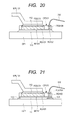
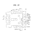
- a crack or peel-off may occur in the bonding material bonding the die pad DP1 to the semiconductor chip CP1 to possibly degrade the accuracy of sensing the current flowing in the power MOSFET QH by means of the sense MOSFET QS. This will be described below with reference to FIGS. 20 and 21 .
- FIGS. 20 and 21 are illustrative views of the problem found by the present inventors, and show a state in which a semiconductor chip CP101 corresponding to the semiconductor chip CP1 is mounted over the die pad DP1 and bonded thereto via a solder 111 and, in addition, the bonding wires BW and a metal plate MPL101 have been coupled to the semiconductor chip CP101.
- resin sealing has been performed, and a semiconductor device (semiconductor package) such as the foregoing semiconductor device PKG has been formed.
- a semiconductor device semiconductor package
- illustration of the foregoing sealing portion MR is omitted.
- FIGS. 20 and 21 are cross-sectional views but, for improved clarity of illustration, hatching of the regions other than a main MOSFET region RG101 and a sense MOSFET region RG102 is omitted.
- a back-side electrode BE101 is formed over the entire back surface of the semiconductor chip CP101.
- the back-side electrode BE101 of the semiconductor chip CP101 is bonded to the die pad DP1 via the solder 111.
- a source pad electrode PDS101 for the foregoing power MOSFET QH and a source pad electrode PDS104 for the foregoing sense MOSFET QS are formed.
- the metal plate MPL101 is bonded via a solder 112.
- the bonding wire BW is coupled.
- the semiconductor chip CP101 is provided with the main MOSFET region RG101 (corresponding to the foregoing main MOSFET region RG1) where the foregoing power MOSFET QH is formed and with the sense MOSFET region RG102 where the foregoing sense MOSFET QS is formed.
- the back-side electrode BE101 corresponds to the foregoing back-side electrode BE
- the pad electrode PDS101 corresponds to the foregoing pad electrode PDS1
- the pad electrode PDS104 corresponds to the foregoing pad electrode PDS4
- the metal plate MPL101 corresponds to the foregoing metal plate MPL.
- the main MOSFET region RG101 corresponds to the foregoing main MOSFET region RG1
- the sense MOSFET region RG102 corresponds to the foregoing sense MOSFET region RG2
- the solder 111 corresponds to the foregoing adhesive layer BD1
- the solder 112 corresponds to the foregoing adhesive layer BD3.
- the sense MOSFET region RG102 is formed at a position two-dimensionally overlapping the pad electrode PDS104 (i.e., position overlapping the pad electrode PDS104 when viewed in a plane parallel with the main surface of the semiconductor chip CP101). Note that in the semiconductor chip CP101 of FIGS. 20 and 21 and the foregoing semiconductor chip CP1, the positions of the sense MOSFET regions RG1 and RG102 are different.
- a current flowing in the foregoing power MOSFET QH flows from the die pad DP1 to the metal plate MPL101 via the solder 111, the back-side electrode BE101, the main MOSFET region RG101 (the foregoing power MOSFET QH formed therein) of the semiconductor chip CP101, the pad electrode PDS101, and the solder 112.
- the configuration of FIG. 20 a current flowing in the foregoing power MOSFET QH flows from the die pad DP1 to the metal plate MPL101 via the solder 111, the back-side electrode BE101, the main MOSFET region RG101 (the foregoing power MOSFET QH formed therein) of the semiconductor chip CP101, the pad electrode PDS101, and the solder 112.
- a current flowing in the foregoing sense MOSFET QS flows from the die pad DP1 to the bonding wires BW via the solder 111, the back-side electrode BE101, the sense MOSFET region RG102 (the foregoing sense MOSFET QS formed therein) of the semiconductor chip CP101, and the pad electrode PDS104.
- a crack (hereinafter denoted by the mark 113 and referred to as the crack 113) may occur in the solder 111. Instead, a peel-off may occur but, in the present embodiment, a description will be given on the assumption that the peel-off is included in the crack.
- FIG. 21 shows a state in which, in FIG. 20 , a thermal stress has caused the crack 113 in the solder 111.
- the solder 111 is interposed between the entire back surface of the semiconductor chip CP101 and the upper surface of the die pad DP1, and the crack 113 that has occurred first in the peripheral portion (outer peripheral portion) of the solder 111 extends therefrom in an inward direction (inner direction).
- the region where the crack 113 has occurred is unlikely to allow a current to pass therethrough, and can no longer function as the path of the current.
- the main MOSFET regions (RG1 and RG101) where MOSFETs forming the power MOSFETs QH are formed and the sense MOSFET regions (RG2 and RG102) where MOSFETs forming the sense MOSFETs QS are formed are present.
- the main MOSFET regions (RG1 and RG101) and the sense MOSFET regions (RG2 and RG102) are different in area (the areas of the main MOSFET regions are larger than those of the sense MOSFET regions).
- the area ratios between the main MOSFET regions (RG1 and RG101) and the sense MOSFET regions (RG2 and RG102) in the semiconductor chips CP1 and CP101 are set so as to provide predetermined ratios, e.g., 20000:1 between currents flowing in the power MOSFETs QH and currents flowing in the sense MOSFETs QS.
- the crack 113 occurs in the solder 111 and a current flows so as to avoid the crack 113
- the area of the main MOSFET region RG101 is larger than that of the sense MOSFET region RG102 and accounts for a considerable proportion of the area of the semiconductor chip CP101
- the resistance of a path in which the current flows from the die pad DP1 into the main MOSFET region RG101 (into the transistors thereof) through the solder 111 is not greatly affected by the presence or absence of the crack 113.
- the area of the sense MOSFET region RG102 is considerably smaller than that of the main MOSFET region RG101 and, if the crack 113 extends under the sense MOSFET region RG102 as shown in FIG.
- the current flowing in the sense MOSFET QS is 1/20000 of the current flowing in the power MOSFET QH.
- the current ratio changes and, consequently, the current flowing in the sense MOSFET QS undesirably becomes smaller than 1/20000 of the current flowing in the power MOSFET QH.
- the sense MOSFET QS which is 1/20000 of the current flowing in the power MOSFET QH in the absence of the crack 113, becomes 1/22000 of the current flowing in the power MOSFET QH due to the occurrence of the crack 113, when the current in the power MOSFET QH no longer has the limit value and exceeds 1.1 times the limit value, the sense MOSFET QS senses the value exceeding the limit value.
- a phenomenon in which the accuracy of sensing the current flowing in the power MOSFET QH by means of the sense MOSFET QH is thus degraded by the crack 113 is accelerated by the occurrence of the crack 113 under the sense MOSFET region RG2.
- the positional relationship between the sense MOSFET region RG2 and the metal plate MPL and the like are adjusted so as not to cause the crack 113 under the sense MOSFET region RG2, as will be described later.
- the problem resulting from the crack 113 described above with reference to FIGS. 20 and 21 occurs particularly remarkably when a bonding material (die bonding material) for die-bonding the semiconductor chip CP101 to the die pad DP1 is a solder, but may also occur when a conductive bonding material (die bonding material) other than a solder is used. Accordingly, the present embodiment is particularly effective when the bonding material (i.e., the foregoing adhesive layer BD1) for die-bonding the semiconductor chip CP1 to the die pad DP1 is a solder, but is also effective when a conductive bonding material other than a solder, e.g., a paste-type conductive bonding material such as a silver paste is used.
- the bonding material i.e., the foregoing adhesive layer BD1
- a conductive bonding material other than a solder e.g., a paste-type conductive bonding material such as a silver paste is used.
- FIG. 22 is an illustrative view of the semiconductor device PKG of the present embodiment, and shows a plan view (top view) showing a state in which the metal plate MPL is bonded to the semiconductor chip CP1.
- FIG. 22 if the semiconductor device PKG is viewed through the metal plate MPL (if the metal plate MPL is removed), the same view as FIG. 13 described above is obtained.
- FIG. 22 is a view showing only the semiconductor chip CP1 and the metal plate MPL of FIG. 7 described above under magnification
- FIG. 13 described above is a view showing only the semiconductor chip CP1 of FIG. 8 described above under magnification. Note that FIG.
- FIG. 22 also shows the sense MOSFET region RG2 but, actually, the sense MOSFET region RG2 is covered with the uppermost-layer protective film (corresponding to the foregoing protective film 12) of the semiconductor chip CP1.
- FIG. 23 is a partially enlarged plan view obtained by enlarging a region 20 enclosed by the two-dot-dash line in FIG. 22 , and shows the layout of the metal plate MPL, the sense MOSFET region RG2, the pad electrode PDS1, and the pad electrode PDS4.
- FIGS. 24 and 25 are illustrative views of the semiconductor device PKG of the present embodiment, and show a state in which the semiconductor chip CP1 is mounted over the die pad DP1 via the adhesive layer BD1 and bonded thereto and, in addition, the bonding wires BW and the metal plate MPL have been coupled to the semiconductor chip CP1.
- resin sealing has been performed (sealing portion MR has been formed), and the semiconductor device PKG as shown in FIGS. 1 to 9 described above has been formed.
- FIGS. 24 and 25 illustration of the foregoing sealing portion MR is omitted. Note that FIGS.
- FIG. 24 and 25 are cross-sectional views but, for improved clarity of illustration, hatching of the regions other than the main MOSFET region RG1 and the sense MOSFET region RG2 is omitted. Since FIG. 24 corresponds to a cross-sectional view at a position along the line A1-A1 in FIGS. 7 and 22 described above and FIG. 25 corresponds to a cross-sectional view at a position along the line A2-A2 in FIGS. 7 and 22 described above, FIG. 24 corresponds to FIG. 3 described above and FIG. 25 corresponds to FIG. 4 described above. In FIG. 22 , the lines A3-A3 and A4-A4 are shown at the same positions as the lines A3-A3 and A4-A4 in FIG. 7 described above.
- FIG. 5 described above corresponds to a cross-sectional view at the position along the line A3-A3 in each of FIGS. 7 to 22 described above
- FIG. 6 described above corresponds to a cross-sectional view at the position along the line A4-A4 in each of FIGS. 7 to 22 described above.
- the lines A2-A2 and A4-A4 in FIGS. 7 and 22 described above extend through (traverse) the sense MOSFET regions RG2, and the lines A1-A1 and A3-A3 in FIGS. 7 and 22 described above do not extend through (do not traverse) the sense MOSFET regions RG2.
- the semiconductor chip CP1 of the present embodiment is formed not only with the power MOSFET QH, but also with the sense MOSFET QS for sensing the current flowing in the power MOSFET QH. That is, the semiconductor chip CP1 of the present embodiment is formed with the power MOSFET QH and the sense MOSFET QS, and has the main MOSFET region RG1 where the vertical MOSFETs corresponding to the power MOSFET QH are formed, and the sense MOSFET region RG2 where the vertical power MOSFETs corresponding to the sense MOSFET QS are formed, as shown in FIG. 14 described above or the like.
- the plurality of pad electrodes PD including the source pad electrodes PDS1, PDS2, PDS3, and PDS4 and the gate pad electrode PDG are formed.
- the pad electrode PDS1 is bonded (coupled) to the metal plate MPL, and the pad electrodes PD (including the pad electrodes PDS2, PDS3, PDS4, and PDG) other than the pad electrode PDS1 are coupled to the bonding wires BW.
- the metal plate MPL and the sense MOSFET region RG2 do not overlap each other, and the three sides of the sense MOSFET region RG2 are surrounded by the metal plate MPL. That is, in the plan view, the sense MOSFET region RG2 has a generally rectangular two-dimensional shape, and the three sides (three sides of the sense MOSFET region RG2) of the four sides of the rectangle oppose the metal plate MPL.
- the pad electrode PDS1 and the sense MOSFET region RG2 do not overlap, and the pad electrode PDS1 surrounds the three sides of the sense MOSFET region RG2. In other words, the three sides of the sense MOSFET region RG2 oppose the pad electrode PDS1.
- the metal plate MPL is bonded to the pad electrode PDS1 of the semiconductor chip CP1. Specifically, the portion of the metal plate MPL two-dimensionally overlapping the pad electrode PDS1 of the semiconductor chip CP1 (in the plan view) is bonded (coupled or adhesively bonded) to the pad electrode PDS1 via the conductive adhesive layer (bonding material) BD. Accordingly, in the plan view, the bonded portion (bonded region) between the metal plate MPL and the pad electrode PDS1 does not overlap the sense MOSFET region RG2, and the bonded portion (bonded region) between the metal plate MPL and the pad electrode PDS1 surrounds the three sides of the sense MOSFET region RG2.
- FIG. 23 is a plan view but, in FIG. 23 , a bonded portion (bonded region) MPLa between the metal plate MPL and the pad electrode PDS1 is shown by hatching.
- the semiconductor chip CP1 and the metal plate MPL are specifically designed as follows.
- a side SD7 (more specifically, in the vicinity of substantially the middle of the side SD7) of the pad electrode PDS1 opposing the side SD1 of the semiconductor chip CP1 is provided with a retracted portion (pad retracted portion, recessed portion, or two-dimensional recessed portion) 21 which is a region where the pad electrode PDS1 is locally (partially) retracted (retracted in the plan view) in a direction away from the side SD1 of the semiconductor chip CP1.
- the sense MOSFET region RG2 is disposed (see FIGS. 13 , 22 , 23 , and the like).
- a front end side (side) SD8 of the metal plate MPL closer to the semiconductor chip CP2 is provided with a retracted portion (metal-plate retracted portion, recessed portion, or two-dimensional recessed portion) 22 which is a region locally (partially) retracted (retracted in the plan view) in a direction away from the semiconductor chip CP2. Then, the metal plate MPL is bonded to the source pad electrode PDS1 such that the sense MOSFET region RG2 is located (disposed) in the retracted portion 22.
- the foregoing three sides of the sense MOSFET region RG2 are three sides 23a, 23b, and 23c denoted by the reference numerals 23a, 23b, and 23c in FIG. 23 .
- the purpose for providing such a state is to minimize, even when a crack corresponding to the foregoing crack 113 is formed in the adhesive layer BD1 bonding the die pad DP1 to the semiconductor chip CP1, the possibility of extension of the crack to a position under the sense MOSFET region RG2 in the adhesive layer BD1, which will be described with reference to FIG. 26 .
- FIG. 26 is a schematic cross-sectional view of the semiconductor device PKG.
- FIG. 26 schematically shows a state in which the semiconductor chip CP1 is mounted over (bonded to the upper surface of) the die pad DP1 via the adhesive layer BD1, and the metal plate MPL is bonded to the semiconductor chip CP1 (to the pad electrode PDS1 thereof) with the adhesive layer BD3, but illustration of the sealing portion MR is omitted therein.
- FIG. 26 is a cross-sectional view, but hatching is omitted therein for improved clarity of illustration.
- the region where the semiconductor chip CP1 is vertically interposed between the metal plate MPL and the die pad DP1 i.e., region where the metal plate MPL is present over the semiconductor chip CP1
- the region where the semiconductor chip CP1 is not vertically interposed between the metal plate MPL and the die pad DP1 i.e., region where the metal plate MPL is not present over the semiconductor chip CP1
- the semiconductor chip CP1 is vertically interposed between the metal plate MPL and the die pad DP1.
- the semiconductor chip CP1 is included in the upper surface of the die pad DP1 so that the die pad DP1 is present under the entire semiconductor chip CP1.
- the top surface of the semiconductor chip CP1 has the region (portion) overlapping the metal plate MPL and the region (portion) not overlapping the metal plate MPL in the plan view. Accordingly, the top surface of the semiconductor chip CP1 has the region where the metal plate MPL is present thereover (i.e., region to which the metal plate MPL is bonded) and the region where the metal plate MPL is not present thereover (i.e., region to which the metal plate MPL is not bonded).
- a two-dimensional region corresponding to the entire semiconductor chip CP1 in the plan view is a combination of the region RG11 where the semiconductor chip CP1 is vertically interposed between the metal MPL and the die pad DP1 and the region RG12 where the semiconductor chip CP1 is not vertically interposed between the metal MPL and the die pad DP1.
- a crack (crack corresponding to the foregoing crack 113) may occur in the adhesive layer BD1 bonding the semiconductor chip CP1 to the die pad DP1.
- One of major causes of the occurrence of the crack in the adhesive layer BD1 is the difference between the amount of thermal expansion (thermal expansion length) of the die pad DP1 and the amount of thermal expansion (thermal expansion length) of the semiconductor chip CP1, which is produced due to the difference between the thermal expansion coefficient (coefficient of thermal expansion) of the die pad DP1 and the thermal expansion coefficient (coefficient of thermal expansion) of the semiconductor chip CP1 when a thermal stress is applied.
- This causes a stress in the adhesive layer BD1 interposed between the semiconductor chip CP1 and the die pad DP1 and a crack in the adhesive layer BD1.
- the thermal expansion coefficient of the die pad DP1 comprised of a metal is larger than the thermal expansion coefficient of the semiconductor chip (mainly comprised of Si) so that, when a thermal stress is applied, the amount of thermal expansion of the die pad DP1 is large and, compared thereto, the amount of thermal expansion of the semiconductor chip CP1 is small.
- the experiment conducted by the present inventors has confirmed that the crack in the adhesive layer BD1 is less likely to be formed in the region RG11 where the semiconductor chip CP1 is vertically interposed between the metal plate MPL and the die pad DP1 (i.e., region where the metal plate MPL is present thereover) than in the region RG12 where the semiconductor chip CP1 is not vertically interposed between the metal plate MPL and the die pad DP1 (i.e., region where the metal plate MPL is not present thereover).
- the following is a conceivable reason for this.
- the semiconductor chip CP1 when a thermal stress is applied, the semiconductor chip CP1 is not only pulled in the direction of thermal expansion by the die pad DP1 located thereunder, but also pulled in the direction of thermal expansion by the metal plate MPL located thereover. Accordingly, the semiconductor chip CP1 is more likely to undergo thermal expansion in the region RG11 than in the region RG12 (i.e., the amount of thermal expansion increases therein). As a result, the difference between the amount of thermal expansion of the die pad DP1 and that of the semiconductor chip CP1 is smaller in the region RG11 than in the region RG12.
- the difference between the amount of thermal expansion of the die pad DP1 and that of the semiconductor chip CP1 is smaller in the region RG11 than in the region RG12, and therefore the stress produced in the adhesive layer BD1 is smaller in the region RG11 than in the region RG12.
- the thermal expansion coefficients of the metal plate MPL and the die pad DP1 are larger than that of the semiconductor chip CP1
- both the metal plate MPL over the semiconductor chip CP1 and the die pad DP1 under the semiconductor chip CP1 operate to pull the semiconductor chip CP1 in the direction of thermal expansion.
- the difference between the amount of thermal expansion of the semiconductor chip CP1 and that of the die pad DP1 is smaller in the region RG11 than in the region RG12, and the stress produced in the adhesive layer BD1 is also smaller in the region RG11. Since the crack in the adhesive layer BD1 is more likely to occur in a place where the stress produced in the adhesive layer BD1 is large, and is less likely to occur in a place where the stress is small, the crack in the adhesive layer BD1 is less likely to occur in the region RG11 than in the region RG12.
- the sense MOSFET region RG2 is disposed in a place corresponding to the region RG11 where the semiconductor chip CP1 is vertically interposed between the metal plate MPL and the die pad DP1 (i.e., region where the metal plate MPL is present over the semiconductor chip CP1) to thereby inhibit a crack from occurring in the adhesive layer BD1 immediately under the sense MOSFET region RG2.
- the sense MOSFET region RG2 is disposed at a position in the semiconductor chip CP1 which allows a reduction in the difference between the amount of thermal expansion of the semiconductor chip CP1 and that of the die pad DP1 to thereby inhibit a crack from occurring in the adhesive layer BD1 immediately under the sense MOSFET region RG2.
- the three sides (23a, 23b, and 23c) of the sense MOSFET region RG2 are surrounded by the metal plate MPL (in other words, the three sides of the sense MOSFET region RG2 oppose the metal plate MPL).
- the three sides (23a, 23b, and 23c) of the sense MOSFET region RG2 are surrounded by the pad electrode PDS1 (in other words, the three sides of the sense MOSFET region RG2 oppose the pad electrode PDS1).
- the bonded portion (MPLa) between the metal plate MPL and the pad electrode PDS1 surrounds the three sides (23a, 23b, and 23c) of the sense MOSFET region RG2 (in other words, the three sides of the sense MOSFET region RG2 oppose the bonded portion between the metal plate MPL and the pad electrode PDS1) .
- the pad electrode PDS1, the metal plate MPL, and the bonded portion MPLa between the metal plate MPL and the pad electrode PDS1 exist in a direction (direction parallel with the side SD1) of approach from the sense MOSFET region RG2 to the side SD2, in a direction (direction perpendicular to the side SD1) of approach from the sense MOSFET region RG2 to the side SD3, and in a direction (direction parallel with the side SD1) of approach from the sense MOSFET region RG2 to the side SD4.
- the source wire 10S1 (source wire 10S1 for the power MOSFET QH), but the source wire 10S2 (source wire 10S2 for the sense MOSFET QS) needs to be disposed. Therefore, it is difficult to extend the source pad electrode PDS1 of the power MOSFET QH to a region immediately over the sense MOSFET region RG2. As a result, the source pad electrode PDS1 of the power MOSFETA QH does not overlap the sense MOSFET region RG2 in the plan view. Consequently, the bonded portion MPLa between the metal plate MPL and the pad electrode PDS1 does not overlap the sense MOSFET region RG2 in the plan view, and the metal plate MPL also does not overlap the sense MOSFET region RG2 in the plan view.
- Such a position at which the sense MOSFET region RG2 is disposed is a place corresponding to the region RG11 described above where the semiconductor chip CP1 is vertically interposed between the metal plate MPL and the die pad DP1 and, in the adhesive layer BD1 located thereunder, a crack is less likely to occur. Therefore, by disposing the sense MOSFET region RG2 at such a position, it is possible to inhibit or prevent a crack from occurring in the adhesive layer BD1 immediately under the sense MOSFET region RG2 (i.e., it is possible to inhibit or prevent a crack corresponding to the foregoing crack 113 from being formed at a position under the sense MOSFET region RG2 in the adhesive layer BD1).
- the source pad electrode PDS4 of the sense MOSFET QS is disposed at a position close to the outer peripheral portion (side SD1) rather than at an inner position over the main surface of the semiconductor chip CP1, it is easier to couple a conductive member such as the bonding wire BW thereto. Therefore, in the present embodiment, over the main surface (top surface) of the semiconductor chip CP1, the sense MOSFET region RG2 and the source pad electrode PDS4 of the sense MOSFET QS are not disposed at the same two-dimensional positions (vertically overlapping positions), but the source pad electrode PDS4 of the sense MOSFET QS is disposed outside the sense MOSFET region RG2 (closer to the side SD1).
- the sense MOSFET region RG2 and the pad electrode PDS4 are disposed such that the pad electrode PDS4 is closer to the outer peripheral portion (side SD1) of the main surface of the semiconductor chip CP1 than the sense MOSFET region RG2.
- a distance (interval) L2 from the outer periphery (side SD1) of the main surface of the semiconductor chip CP1 to the pad electrode PDS4 is adjusted to be smaller (shorter) than a distance (interval) L1 from the outer periphery (side SD1) of the main surface of the semiconductor chip CP1 to the sense MOSFET region RG2 (i.e., L1 > L2 is satisfied.
- the source pad electrode PDS4 of the sense MOSFET QS is disposed closer to the side SD1 of the main surface of the semiconductor chip CP1 than the sense MOSFET region RG2.
- a crack is inhibited or prevented from being formed at a position under the sense MOSFET region RG2 in the adhesive layer BD1 to improve the accuracy of sensing a current flowing in the power MOSFET QH by means of the sense MOSFET QS.
- the pad electrode PDS4 outside the sense MOSFET region RG2 (i.e., disposing the pad electrode PDS4 closer to the side SD1 than the sense MOSFET region RG2), it is possible to easily couple a conductive member such as the bonding wire BW to the source pad electrode PDS4 of the sense MOSFET QS.
- the source region (corresponding to the foregoing semiconductor region 4 of the sense MOSFET region RG2) of the sense MOSFET QS formed in the sense MOSFET region RG2 is electrically coupled to the source pad electrode PDS4 of the sense MOSFET QS via (through) the foregoing source wire (wire for source) 10S2 formed in the semiconductor chip CP1.
- the pad electrode PDS1, the metal plate MPL, and the bonded portion MPLa between the metal plate MPL and the pad electrode PDS1 are not located (do not exist).
- the pad electrode PDS1, the metal plate MPL, and the bonded portion MPLa between the metal plate MPL and the pad electrode PDS1 do not exist in a direction (direction perpendicular to the side SD1) of approach from the sense MOSFET region RG2 to the side SD1.
- the semiconductor chip CP1 is disposed between the lead L1 and the semiconductor chip CP2, and the main surface (top surface) of the semiconductor chip CP1 has the side (chip side) SD1 closer to the semiconductor chip CP2 and the side (chip side) SD3 opposing the side (chip side) SD1 (see FIGS. 7 and 8 described above).
- the sense MOSFET region RG2 is disposed to be closer to the side SD1 than to the side SD3.
- a distance (interval) L3 between a front end side (side) SD8 of the metal plate MPL opposing the semiconductor chip CP2 and the side (chip side) SD1 thereof is not more than the distance (interval) L1 between the sense MOSFET region RG2 and the side (chip side) SD1 (i.e., L1 ⁇ L3 is satisfied.
- the distances L1, L2, and L3 and distances L4 and L5 described later correspond to distances along a direction perpendicular to the side SD1.
- FIG. 27 is a plan view of the structure of FIG. 20 described above, and shows a plan view corresponding to FIG. 22 described above.
- FIG. 28 is a partially enlarged plan view obtained by enlarging a region 120 enclosed by the two-dot-dash line in FIG. 27 , and shows the position of the sense MOSFET region RG102 by the dotted line.
- a distance L101 between the sense MOSFET region RG102 and a side (chip side) SD101 of the semiconductor chip CP101 is smaller (shorter) than a distance L103 between a front end side SD108 of the metal plate MPL101 and the side (chip side) SD101 of the semiconductor chip CP101 (i.e., L101 ⁇ L103 is satisfied).
- the side SD101 corresponds to the foregoing side SD1
- the front end side SD108 corresponds to the foregoing front end side SD8.
- a region closer to the side SD101 than to the front end side SD108 of the metal plate MPL is located outside the foregoing region RG11 where the semiconductor chip CP101 is vertically interposed between the metal plate MP101 and the die pad DP1. Accordingly, a crack is more likely to occur in the foregoing solder 111 located thereunder than in the region RG11. Therefore, in the case of FIGS.
- the distance L3 between the front end side SD8 of the metal plate MPL and the side (chip side) SD1 of the semiconductor chip CP1 is not more than the distance L1 between the sense MOSFET region RG2 and the side (chip side) SD1 (i.e., L3 ⁇ L1 is satisfied). That is, in the present embodiment over the main surface (top surface) of the semiconductor chip CP1, the sense MOSFET region RG2 is disposed at a position inward of the front end side SD8 of the metal plate MPL. This allows a reduction in the difference between the amount of thermal expansion of the semiconductor chip CP1 and that of the die pad DP1 at the position at which the sense MOSFET region RG2 is formed.
- the metal plate MPL and the die pad DP1 between which the semiconductor chip CP1 is interposed are formed of the same material. This is because, if the metal plate MPL and the die pad DP1 are formed of the same material, the thermal expansion coefficient (coefficient of thermal expansion) of the metal plate MPL and the thermal expansion coefficient (coefficient of thermal expansion) of the die pad DP1 are the same so that, when a thermal stress is applied, the metal plate MPL located over the semiconductor chip CP1 and the die pad DP1 located thereunder operate to pull the semiconductor chip CP1 to the same degree in the direction of thermal expansion. As a result, it is possible to more reliably obtain the effect of inhibiting or preventing a crack from occurring in the adhesive layer BD1 immediately under the sense MOSFET region RG2.
- the die pad DP1 is also preferably formed of aluminum (Al) or an aluminum (Al) alloy, which is the same material as that of the metal plate MPL.
- the die pad DP1 is also preferably formed of copper (Cu) or a copper (Cu) alloy, which is the same material as that of the metal plate MPL.
- copper (Cu) or a copper (Cu) alloy is particularly preferred as the materials of the metal plate MPL and the die pad DP1.
- each of the die pad DP2 and the leads LD is also formed of the same material as those of the die pad DP1 and the metal plate MPL, the die pad DP1, the die pad DP2, and the leads LD can be formed using a lead frame, which more desirably facilitates the manufacturing of the semiconductor device PKG.
- the adhesive layer BD3 bonding the metal plate MPL to the pad electrode PDS1 of the semiconductor chip CP1 is formed of the same material as that of the adhesive layer BD1 bonding the semiconductor chip CP1 to the die pad DP1. That is, in the case of using a solder for the adhesive layer BD1 bonding the semiconductor chip CP1 to the die pad DP1, it is preferable to use a solder also for the adhesive layer BD3 bonding the metal plate MPL to the pad electrode PDS1 of the semiconductor chip CP1.
- the semiconductor chip CP1 of the first modification will be hereinafter denoted by the mark CP1a and referred to as a semiconductor chip CP1a.
- FIGS. 29 to 31 are plan views each showing the chip layout of the semiconductor chip CP1a, and respectively correspond to FIGS. 13 to 15 described above.
- FIG. 29 corresponds to a top view of the semiconductor chip CP1a, and shows the top surface side (i.e., main surface formed with the pad electrodes PD) of the semiconductor chip CP1a.
- FIG. 29 is a plan view but, for easier understanding, the bonding pads (pad electrodes PD including the pad electrodes PDG, PDS1, PDS2, PDS3, PDS4, PDA, and PDC) are hatched therein. Note that, for easier understanding, FIG.
- FIG. 29 also shows the sense MOSFET region RG2 and a diode region (diode formation region) RG3 but, actually, the sense MOSFET region RG2 and the diode region RG3 are covered with the uppermost-layer protective film (corresponding to the foregoing protective film 12) of the semiconductor chip CP1.
- FIG. 30 is a plan view, but shows the main MOSFET region RG1, the sense MOSFET region RG2, and the diode region RG3 in the semiconductor chip CP1a by hatching, and shows the positions of the bonding pads (pad electrodes PDG, PDS1, PDS2, PDS3, PDS4, PDA, and PDC) by the dotted lines.
- FIG. 31 is a plan view, but shows the layout of the source wires 10S1 and 10S2, an anode wire 10A, and a cathode wire 10C in the semiconductor chip CP1a by the hatched regions, and shows the positions of the bonding pads (pad electrodes PDG, PDS1, PDS2, PDS3, PDS4, PDA, and PDC) by the dotted lines. Note that the positions of the bonding pads (pad electrodes PDG, PDS1, PDS2, PDS3, PDS4, PDA, and PDC) shown by the dotted lines in FIGS. 30 and 31 correspond to the regions shown by hatching in FIG. 29 .
- FIG. 32 is a partially enlarged plan view (main-portion plan view) of the semiconductor chip CP1a, which is obtained by enlarging a region 20a enclosed by the two-dot-dash line in FIG. 29 , and shows the layout of the main MOSFET region RG1, the sense MOSFET region RG2, the diode region RG3, the pad electrodes PDS1, PDS4, PDA, and PDC, the source wires 10S1 and 10S2, the anode wire 10A, and the cathode wire 10C.
- FIG. 33 is a plan view (top view) showing a state in which the metal plate MPL is bonded to the semiconductor chip CP1a, and corresponds to FIG. 22 described above. Note that FIG.
- FIG. 33 also shows the sense MOSFET region RG2 and the diode region RG3 but, actually, the sense MOSFET region RG2 and the diode region RG3 are covered with the uppermost-layer protective film (corresponding to the foregoing protective film 12).
- FIG. 34 is a partially enlarged plan view obtained by enlarging the region 20a enclosed by the two-dot-dash line in FIG. 33 , corresponds to FIG. 23 described above, and shows the layout of the metal plate MPL, the sense MOSFET region RG2, the diode region RG3, and the pad electrodes PDS1, PDS4, PDA, and PDC. Note that FIG.
- FIG. 34 is a plan view, but shows the bonded portion (bonded region) MPLa between the metal plate MPL and the pad electrode PDS1 by hatching.
- FIG. 35 is a main-portion cross-sectional view of the semiconductor chip CP1a, and shows a cross section passing through (traversing) the diode region RG3 and the pad electrode PDA.
- the semiconductor chip CP1a not only the foregoing power MOSFET QH (main MOSFET region RG1) and the sense MOSFET QS (sense MOSFET region RG2), but also a temperature sensing diode (diode element) is formed, and the region where the diode is formed is the diode region RG3.
- the semiconductor chip CP1a has the main MOSFET region RG1 where the foregoing power MOSFET QH is formed, the sense MOSFET region RG2 where the foregoing sense MOSFET QS is formed, and the diode region RG3 where the temperature sensing diode (diode element) is formed.
- the diode formed in the diode region RG3 is a diode (circuit) for sensing the temperature of the power MOSFET QH.
- the diode can also be regarded as a diode (circuit) for sensing heat generated from the power MOSFET QH, and is disposed in the vicinity of the power MOSFET QH in the semiconductor chip CP1a to allow the temperature of the power MOSFET QH (heat generated therefrom) to be sensed.
- the diode formed in the diode region RG3 can also be regarded as a temperature sensing circuit.
- the anode of the diode formed in the diode region RG3 is electrically coupled to an anode pad electrode PDA via the anode wire 10A, while the cathode of the diode formed in the diode region RG3 is electrically coupled to a cathode pad electrode PDC via the cathode wire 10C.
- the anode wire 10A and the cathode wire 10C are each formed of the foregoing patterned conductor film 10. Accordingly, the anode wire 10A and the cathode wire 10C are wires in the same layer as the foregoing source wires and the foregoing gate wire 10G.
- the semiconductor chip CP1a has, as pad electrodes, the anode pad electrode PDA for the diode formed in the diode region RG3 and the cathode pad electrode PDC for the diode formed in the diode region RG3 in addition to the source pad electrodes PDS1, PDS2, PDS3, and PDS4 and the gate pad electrode PDG.
- the foregoing bonding wires BW are coupled and, via the foregoing bonding wires BW (each having one end thereof coupled to the pad electrode PDA or the pad electrode PDC and the other end thereof coupled to the pad electrode PD2 of the semiconductor chip CP2), the anode pad electrode PDA and the cathode pad electrode PDC are electrically coupled to the control circuit CLC formed in the foregoing semiconductor chip CP2.
- the diode Since the diode has a voltage-current characteristic which changes in accordance with the temperature, by sensing (monitoring) the voltage-current characteristic of the diode formed in the diode region RG3, it is possible to sense the temperature of the diode in the semiconductor chip CP1a. Therefore, by disposing the diode region RG3 (diode) in the vicinity of the power MOSFET QH in the semiconductor chip CP1a, it is possible to sense the temperature of the power MOSFET QH (heat generated therefrom) by means of the diode.
- the voltage of the diode (voltage between the anode and cathode thereof) formed in the diode region RG3 in a state in which a constant current is allowed to flow in the diode, and obtain the temperature of the diode from the resulting voltage value. That is, the voltage when the constant current is allowed to flow in the diode is lower as the temperature is higher, and therefore it is possible to sense the temperature of the diode using the voltage.
- the supply of the constant current to the diode formed in the diode region RG3 and the sensing of the voltage of the diode (voltage between the anode and cathode thereof) can be performed using the control circuit CLC of the foregoing semiconductor chip CP2.
- the foregoing driver circuit DR of the foregoing control circuit CLC supplies the OFF signal to the gate of the power MOSFET QH (or stops the supply of the ON signal) to thereby switch the power MOSFET QH into the OFF state.
- the power MOSFET QH when the power MOSFET QH generates excessive heat, it is possible to sense the generation of the excessive heat by means of the diode in the diode region RG3, and swiftly switch the power MOSFET QH into the OFF state.
- the foregoing load LA is short-circuited in a state in which the power MOSFET QH has been turned ON and a voltage is applied from the foregoing power source BT to the foregoing load LA
- a large current (current larger than during normal operation) undesirably flows in the power MOSFET QH so that the power MOSFET QH generates excessive heat.
- the power MOSFET QH can be swiftly switched into the OFF state.
- the semiconductor chip CP1 has the diode region RG3 where the temperature sensing diode (diode element) is formed.
- the diode (diode formed in the diode region RG3) can be formed of a diode DD1 using a PN junction as shown in FIG. 35 .
- a polysilicon film 31 for forming the diode is formed over the field insulating film (isolation region) 2.
- the polysilicon film 31 has an n-type silicon portion (n-type silicon region) 31a into which an n-type impurity (e.g., phosphorus) has been introduced, and a p-type silicon portion (p-type silicon region) 31b into which a p-type impurity (e.g., boron) has been introduced.
- the n-type silicon portion 31a and the p-type silicon portion 31b are adjacent to each other, and a PN junction is formed at the interface between the p-type silicon portion 31b and the n-type silicon portion 31a.
- the polysilicon film 31 can also be formed of the conductive film in the same layer as the gate electrodes 7 and the wiring portions 7a for gate extraction, but the polysilicon film 31 and the gate electrodes 7 (and the wiring portions 7a for gate extraction) are isolated from each other and are not electrically coupled to each other.
- the p-type silicon portion 31b of the polysilicon film 31 formed in the diode region RG3 serves as the anode of the diode DD1
- the n-type silicon portion 31a of the polysilicon film 31 formed in the diode region RG3 serves as the cathode of the diode DD1.
- the anode wire 10A is electrically coupled to the p-type silicon portion 31b of the polysilicon film 31 through a contact hole (opening or through hole) 9c formed in the insulating film 8
- the cathode wire 10C is electrically coupled to the n-type silicon portion 31a of the polysilicon film 31 through a contact hole (opening or through hole) 9d formed in the insulating film 8.
- the anode wire 10A and the cathode wire 10C are formed in the same layer as the foregoing gate wire 10G and the source wires 10S1 and 10S2 (i.e., formed of the foregoing patterned conductor film 10).
- the anode wire 10A exposed from the opening 13 in the protective film 12 forms the anode pad electrode PDA of the foregoing diode DD1
- the cathode wire 10C exposed from the opening 13 of the protective film 12 forms the cathode pad electrode PDC of the foregoing diode DD1.
- the sense MOSFET region RG2 is disposed in the retracted portion 21 in which the pad electrode PDS1 is locally (partially) retracted in the direction away from the side SD1 of the semiconductor chip CP1.
- the sense MOSFET region RG2 and the diode region RG3 are disposed in the retracted portion 21.
- the metal plate MPL is bonded to the source pad electrode PDS1 such that the sense MOSFET region RG2 and the diode region RG3 are located (disposed) in the retracted portion 22 of the front end side SD8 of the metal plate MPL.
- the semiconductor chip CP1a instead of the semiconductor chip CP1
- the semiconductor chip CP1a when attention is focused on the two-dimensional positional relationship among the metal plate MPL, the sense MOSFET region RG2, and the diode region RG3, in the plan view, the three sides of the sense MOSFET region RG2 and the three sides of the diode region RG3 are surrounded by the metal plate MPL (in other words, the three sides of the sense MOSFET region RG2 and the three sides of the diode region RG3 oppose the metal plate MPL).
- the three sides of the sense MOSFET region RG2 and the three sides of the diode region RG3 are surrounded by the pad electrode PDS1 (in other words, the three sides of the sense MOSFET region RG2 and the three sides of the diode region RG3 oppose the pad electrode PDS1).
- the bonded portion (MPLa) between the metal plate MPL and the pad electrode PDS1 surrounds the three sides of the sense MOSFET region RG2 and the three sides of the diode region RG3 (in other words, the three sides of the sense MOSFET region RG2 and the three sides of the diode region RG3 oppose the bonded portion between the metal plate MPL and the pad electrode PDS1).
- the pad electrode PDS1, the metal plate MPL, and the bonded portion MPLa between the metal plate MPL and the pad electrode PDS1 exist in the direction (direction parallel with the side SD1) of approach from the sense MOSFET region RG2 to the side SD2, in the direction (direction perpendicular to the side SD1) of approach from the sense MOSFET region RG2 to the side SD3, and in the direction (direction parallel with the side SD1) of approach from the sense MOSFET region RG2 to the side SD4.
- the pad electrode PDS1, the metal plate MPL, and the bonded portion MPLa between the metal plate MPL and the pad electrode PDS1 exist in a direction (direction parallel with the side SD1) of approach from the diode region RG3 to the side SD2, in a direction (direction perpendicular to the side SD1) of approach from the diode region RG3 to the side SD3, and in a direction (direction parallel with the side SD1) of approach from the diode region RG3 to the side SD4.
- the pad electrode PDS1, the metal plate MPL, and the bonded portion MPLa between the metal plate MPL and the pad electrode PDS1 do not exist in the direction (direction perpendicular to the side SD1) of approach from the sense MOSFET region RG2 to the side SD1. Also, in the plan view, the pad electrode PDS1, the metal plate MPL, and the bonded portion MPLa between the metal plate MPL and the pad electrode PDS1 do not exist in a direction (direction perpendicular to the side SD1) of approach from the diode region RG3 to the side SD1.
- the sense MOSFET region RG2 and the diode region RG3 are disposed to be closer to the side SD1 than to the side SD3.
- the distance (interval) L3 between the front end side SD8 of the metal plate MPL and the side SD1 thereof is adjusted to be not more than the distance (interval) L1 between the sense MOSFET region RG2 and the side SD1, and not more than the distance (interval) L4 between the diode region RG3 and the side SD1 (i.e., L1 ⁇ L3 and L4 ⁇ L3 are satisfied. See FIG. 34 ).
- the anode pad electrode PDA and the cathode pad electrode PDC are disposed outside the diode region RG3 (closer to the side SD1). In other words, over the main surface of the semiconductor chip CP1a, the anode pad electrode PDA and the cathode pad electrode PDC are disposed closer to the side SD1 of the main surface of the semiconductor chip CP1a than the diode region RG3.
- the distance (interval) L5 from the side SD1 of the semiconductor chip CP1a to the pad electrode PDA and a distance (interval) L6 from the side SD1 of the semiconductor chip CP1a to the pad electrode PDC are adjusted to be smaller (shorter) than the distance (interval) L4 from the side SD1 of the semiconductor chip CP1a to the diode region RG3 (i.e., L4 > L5 and L4 > L6 are satisfied. See FIG. 34 ).
- a conductive member such as the bonding wire BD
- the configuration of the semiconductor chip CP1a is otherwise basically the same as that of the foregoing semiconductor chip CP1, and the configuration of the semiconductor device PKG using the semiconductor chip CP1a is otherwise basically the same as that of the semiconductor device PKG of FIGS. 1 to 9 described above. Therefore, a description thereof is omitted herein.
- FIG. 36 is a plan view showing the modification of the semiconductor chip CP1a of the first modification, which corresponds to FIG. 33 described above and shows a state in which the metal plate MPL is bonded to the semiconductor chip CP1. Note that FIG. 36 also shows the sense MOSFET region RG2 and the diode region RG3 but, actually, the sense MOSFET region RG2 and the diode region RG3 are covered with the uppermost-layer protective film (corresponding to the foregoing protective film 12) of the semiconductor chip CP1a.
- FIG. 37 is a partially enlarged plan view obtained by enlarging a region 20b enclosed by the two-dot-dash line in FIG. 36 , corresponds to FIG.
- FIG. 37 is a plan view but, in FIG. 37 , the bonded portion (bonded region) MPLa between the metal plate MPL and the pad electrode PDS1 is shown by hatching.
- the pad electrode PDS1 and the metal plate MPL do not extend (are not disposed) between the sense MOSFET region RG2 and the diode region RG3.
- the pad electrode PDS1 and the metal plate MPL extend (are disposed) between the sense MOSFET region RG2 and the diode region RG3. That is, in the case of FIGS.
- the bonded portion MPLa between the pad electrode PDS1 and the metal plate MPL does not extend (is not disposed) between the sense MOSFET region RG2 and the diode region RG3 while, in the case of FIGS. 36 and 37 , in the plan view, the bonded portion MPLa between the pad electrode PDS1 and the metal plate MPL extends (is disposed) between the sense MOSFET region RG2 and the diode region RG3.
- the side SD7 of the pad electrode PDS1 is provided with the one retracted portion 21 in which the pad electrode PDS1 is locally retracted in the direction away from the side SD1 of the semiconductor chip CP1 and, in the same retracted portion 21, the sense MOSFET region RG2 and the diode region RG3 are disposed.
- the metal plate MPL the front end side SD8 thereof is provided with the one retracted portion 22 which is locally retracted in the direction away from the semiconductor chip CP2.
- the metal plate MPL is bonded to the source pad electrode PDS1 such that the sense MOSFET region RG2 and the diode region RG3 are located in the retracted portion 22.
- the side SD7 of the pad electrode PDS1 is provided with two retracted portions 21 and 21a in each of which the pad electrode PDS1 is locally retracted in the direction away from the side SD1 of the semiconductor chip CP1.
- the sense MOSFET region RG2 is disposed while, in the other retracted portion 21a, the diode region RG3 is disposed.
- the metal plate MPL the front end side SD8 thereof is provided with two retracted portions 22 and 22a each of which is locally retracted in the direction away from the semiconductor chip CP2.
- the metal plate MPL is bonded to the source pad electrode PDS1 such that the sense MOSFET region RG2 is located in the one retracted portion 22 and the diode region RG3 is located in the other retracted portion 22a.
- the pad electrode PDS1 and the metal plate MPL extend (accordingly, the bonded portion MPLa between the pad electrode PDS1 and the metal plate MPL extends) between the sense MOSFET region RG2 and the diode region RG3.
- the pad electrode PDS1 and the metal plate MPL do not extend between the sense MOSFET region RG2 and the diode region RG3, which is advantageous in terms of the workability of the metal plate.
- the semiconductor chip CP1 of the second modification is denoted by the mark CP1b and referred to as a semiconductor chip CP1b. It is also assumed that the semiconductor device PKG using the semiconductor chip CP1b instead of the semiconductor chip CP1 is denoted by the mark PKGb and referred to as a semiconductor device PKGb.
- FIG. 38 is a perspective plan view (top view) of the semiconductor device PKGb, and shows a perspective plan view of the top surface side of the semiconductor device PKGb when the semiconductor device PKGb is viewed through the sealing portion MR.
- FIGS. 39 to 41 are cross-sectional views of the semiconductor device PKGb.
- the cross-sectional view of the semiconductor device PKGb at the position along the line C1-C1 of FIG. 38 substantially corresponds to FIG. 39 .
- the cross-sectional view of the semiconductor device PKGb at the position along the line C2-C2 of FIG. 38 substantially corresponds to FIG. 40 .
- the cross-sectional view of the semiconductor device PKGb at the position along the line C3-C3 of FIG. 38 substantially corresponds to FIG. 41.
- FIG. 41 is a perspective plan view (top view) of the semiconductor device PKGb, and shows a perspective plan view of the top surface side of the semiconductor device PKGb when the semiconductor device PKGb is viewed through the sealing portion MR.
- FIG. 42 is a plan view (top view) showing a state in which metal plates MPL1 and MPL2 are bonded to the semiconductor chip CP1b, and corresponds to FIG. 22 described above. It can also be said that FIG. 42 is a view showing only the semiconductor chip CP1b and the metal plates MPL1 and MPL2 in FIG. 38 under magnification. Note that FIG. 42 also shows sense MOSFET regions RG2a and RG2b but, actually, the sense MOSFET regions RG2a and RG2b are covered with the uppermost-layer protective film (corresponding to the foregoing protective film 12) of the semiconductor chip CP1b.
- FIG. 42 also shows sense MOSFET regions RG2a and RG2b but, actually, the sense MOSFET regions RG2a and RG2b are covered with the uppermost-layer protective film (corresponding to the foregoing protective film 12) of the semiconductor chip CP1b.
- FIG. 42 also shows sense MOSFET regions RG2a and RG2b but,
- FIG. 43 is a partially enlarged plan view obtained by enlarging a region 20c enclosed by the two-dot-dash line in FIG. 42 , and corresponds to FIG. 23 described above.
- FIG. 43 is a plan view but, in FIG. 43 , the bonded portion (bonded region) MPLa between the metal plate MPL1 and the pad electrode PDS1 is shown by hatching. Note that a partially enlarged plan view obtained by enlarging a region 20d enclosed by the two-dot-dash line is also the same as FIG. 43.
- FIG. 44 is a partially enlarged plan view (main-portion plan view) of the semiconductor chip CP1b, and corresponds to FIG. 16 described above. FIG. 44 shows the same two-dimensional region as shown in FIG.
- FIG. 45 is a circuit diagram (circuit block diagram) of the semiconductor device PKGb.
- the portion enclosed by the two-dot-dash line is formed of the semiconductor device PKGb
- the portion enclosed by the dotted line denoted by the mark RG21 is formed of a first MOSFET region RG21 of the semiconductor chip CP1
- the portion enclosed by the dotted line denoted by the mark RG22 is formed of a second MOSFET region RG22 of the semiconductor chip CP1.
- the semiconductor device PKGb has 2-channel outputs, and the semiconductor chip CP1b includes the first MOSFET region RG21 and the second MOSFET region RG22.
- the first MOSFET region RG21 and the second MOSFET region RG22 are disposed to be arranged on both sides (both sides in a direction parallel with the side SD1) of the semiconductor chip CP1b, and electrically isolated from each other by an isolation insulating film (corresponding to the foregoing field insulating film 2). That is, when viewed in two dimensions, about a half of the semiconductor chip CP1b corresponds to the first MOSFET region RG21, and the remaining half thereof corresponds to the second MOSFET region RG22.
- the semiconductor chip CP1b is equally divided into two sections (regions) between the opposing two sides SD2 and SD4 of the semiconductor chip CP1b in two dimensions, one of the sections corresponds to the first MOSFET region RG21, while the other section corresponds to the second MOSFET region RG22.
- the first MOSFET region RG21 has basically the same structure as that of the foregoing semiconductor chip CP1, and the second MOSFET region RG22 also has basically the same structure as that of the foregoing semiconductor chip CP1. That is, the semiconductor chip CP1b has such a configuration as obtained by joining the side SD2 of the foregoing semiconductor chip CP1 and the side SD4 of another of the same semiconductor chip CP1, and integrating the two semiconductor chips CP1 with each other.
- the first MOSFET region RG21 and the second MOSFET region RG22 have basically the same configurations, but it is also possible to provide the first MOSFET region RG21 and the second MOSFET region RG22 with mirror-symmetrical (mirror-symmetrical with respect to a virtual boundary line between the first MOSFET region RG21 and the second MOSFET region RG22) configurations.
- the circuit configuration of the semiconductor device PKGb has two systems of the circuit configuration of FIG. 12 described above.
- one switch power MOSFET QH (hereinafter referred to as a power MOSFET QH1) and a sense MOSFET QS for sensing a current flowing in the power MOSFET QH1 (hereinafter referred to as a sense MOSFET QS1) are formed.
- a power MOSFET QH2 In the second MOSFET region RG22 of the semiconductor chip CP1b, one switch power MOSFET QH (hereinafter referred to as a power MOSFET QH2) and a sense MOSFET QS for sensing a current flowing in the power MOSFET QH2 (hereinafter referred to as a sense MOSFET QS2) are formed.
- the semiconductor chip CP2 has a control circuit CLC1 for controlling the power MOSFET QH1 and the sense MOSFET QS1 which are formed in the first MOSFET region RG21 of the semiconductor chip CP1b, and a control circuit CLC2 for controlling the power MOSFET QH2 and the sense MOSFET QS2 which are formed in the second MOSFET region RG22 of the semiconductor chip CP1b.
- the circuit configuration of the power MOSFET QH1, the sense MOSFET QS1, and the control circuit CLC1 of FIG. 45 is basically the same as the circuit configuration of the power MOSFET QH, the sense MOSFET QS, and the control circuit CLC of FIG. 12 described above.
- the circuit configuration of the power MOSFET QH2, the sense MOSFET QS2, and the control circuit CLC2 of FIG. 45 is basically the same as the circuit configuration of the power MOSFET QH, the sense MOSFET QS, and the control circuit CLC of FIG. 12 described above.
- the drains (common drain) of the power MOSFET QH1 and QH2 are coupled to the power source (such as a battery) BT disposed outside the semiconductor device PKGb.
- the source of the power MOSFET QH1 and the source of the power MOSFET QH2 are not short-circuited.
- the source of the power MOSFET QH1 is coupled to a load LA1 disposed outside the semiconductor device PKGb, while the source of the power MOSFET QH2 is coupled to a load LA2 disposed outside the semiconductor device PKGb.
- the gate of the power MOSFET QH1 is coupled to the driver circuit DR of the control circuit CLC1, while the gate of the power MOSFET QH2 is coupled to the driver circuit DR of the control circuit CLC2.
- the power MOSFET QH1 When the power MOSFET QH1 is brought into the ON state by supplying an ON signal from the driver circuit DR of the control circuit CLC1 to the gate of the power MOSFET QH1, the voltage of the power source BT is outputted from the power MOSFET QH1 and supplied to the load LA1.
- the power MOSFET QH1 When the power MOSFET QH1 is brought into the OFF state by supplying an OFF signal from the driver circuit DR of the control circuit CLC1 to the gate of the power MOSFET QH1 (or by stopping the supply of the ON signal), the supply of the voltage from the power source BT to the load LA1 is stopped.
- the power MOSFET QH2 When the power MOSFET QH2 is brought into the ON state by supplying an ON signal from the driver circuit DR of the control circuit CLC2 to the gate of the power MOSFET QH2, the voltage of the power source BT is outputted from the power MOSFET QH2 and supplied to the load LA2.
- the power MOSFET QH2 When the power MOSFET QH2 is brought into the OFF state by supplying an OFF signal from the driver circuit DR of the control circuit CLC2 to the gate of the power MOSFET QH2 (or by stopping the supply of the ON signal), the supply of the voltage from the power source BT to the load LA2 is stopped. Since the power MOSFETs QH1 and QH2 are independently controlled by the control circuits CLC1 and CLC2, the ON/OFF switching of the power MOSFET QH1 and the ON/OFF switching of the power MOSFET QH2 can be independently controlled.
- the semiconductor device PKGb can function as a switch semiconductor device which performs the ON/OFF switching of the application of the voltage from the power source BT to the load LA1 and the ON/OFF switching of the application of the voltage from the power source BT to the load LA2.
- the semiconductor chip CP1 can also be regarded as a semiconductor device having 2-system output circuits (i.e., power MOSFET QH1 and power MOSFET QH2).
- any electronic devices (or electronic components) desired to be coupled to the power source BT via the switch semiconductor device PKGb can be used appropriately.
- the semiconductor device PKGb is particularly useful.
- the semiconductor device PKGb is particularly useful.
- the sense MOSFET QS1 for sensing a current in the power MOSFET QH1 and the sense MOSFET QS2 for sensing a current in the power MOSFET QH2 are provided.
- the power MOSFET QH1 and the sense MOSFET QS1 are formed in the first MOSFET region RG21 of the semiconductor chip CP1b, while the power MOSFET QH2 and the sense MOSFET QS2 are formed in the second MOSFET region RG22 of the semiconductor chip CP1b.
- the power MOSFET QH1 is formed in the foregoing main MOSFET region RG1 of the first MOSFET region RG21 of the semiconductor chip CP1b
- the sense MOSFET QS1 is formed in the foregoing sense MOSFET region RG2 (hereinafter referred to as the sense MOSFET region RG2a) of the first MOSFET region RG21 of the semiconductor chip CP1b.
- the power MOSFET QH2 is formed in the foregoing main MOSFET region RG1 of the second MOSFET region RG22 of the semiconductor chip CP1b
- the sense MOSFET QS2 is formed in the foregoing sense MOSFET region RG2 (hereinafter referred to as the sense MOSFET region RG2b) of the second MOSFET region RG22 of the semiconductor chip CP1b.
- the source pad electrode PDS1 (hereinafter referred to as a pad electrode PDS1a) of the power MOSFET QH1 and the source pad electrode PDS4 (hereinafter referred to as a pad electrode PDS4a) of the sense MOSFET QS1 are formed.
- the source pad electrode PDS1 (hereinafter referred to as a pad electrode PDS1b) of the power MOSFET QH2 and the source pad electrode PDS4 (hereinafter referred to as a pad electrode PDS4b) of the sense MOSFET QS2 are formed.
- the same metal plate MPL1 as the foregoing metal plate MPL is coupled to the pad electrode PDS1a and the bonding wire BW is coupled to the pad electrode PDS4a
- the same metal plate MPL2 as the foregoing metal plate MPL is coupled to the pad electrode PDS1b and the bonding wire BW is coupled to the pad electrode PDS4b.
- illustration of the foregoing pad electrodes PDS2 and PDS3 is omitted, but the foregoing pad electrodes PDS2 and PDS3 are also formed in the first MOSFET region RG21 and the second MOSFET region RG22, respectively.
- one of the leads LD1 is electrically coupled to the pad electrode PDS1a of the semiconductor chip CP1b via the metal plate MPL1, while another of the leads LD1 of the semiconductor chip CP1b is electrically coupled to the pad electrode PDS1b via the metal plate MPL2.
- the five leads LD1 are disposed over the side surface MRc1 of the sealing portion MR.
- two have the inner lead portions thereof that are integrally coupled to each other in the sealing portion MR such that the metal plate MPL1 is coupled thereto via the foregoing adhesive layer BD4, and other two have the inner lead portions thereof that are integrally coupled to each other in the sealing portion MR such that the metal plate MPL2 is coupled thereto via the foregoing adhesive layer BD4.
- the leads LD1 to which the metal plate MPL1 is coupled i.e., the leads LD1 electrically coupled to the pad electrode PDS1a of the semiconductor chip CP1 through the metal plate MPL1
- the leads LD1 to which the metal plate MPL2 is coupled i.e., the leads LD1 electrically coupled to the pad electrode PDS1b of the semiconductor chip CP1 through the metal plate MPL2
- the plurality of leads LD1 are disposed.
- the plurality of leads LD1 may also include a dummy lead LD1D which is not electrically coupled to any of the pad electrodes of the semiconductor chips CP1 and CP2.
- the two-dimensional positional relationship between the sense MOSFET region RG2a of the semiconductor chip CP1b and the source pad electrode PDS1a thereof, the two-dimensional positional relationship between the sense MOSFET region RG2a and the metal plate MPL1, and the two-dimensional positional relationship between the sense MOSFET region RG2a and the bonded portion between the metal plate MPL1 and the pad electrode PDS1a are the same as in the case of the foregoing semiconductor chip CP1 ( FIGS. 16 and 23 ).
- the two-dimensional positional relationship between the sense MOSFET region RG2a and the source pad electrode PDS4a is the same as in the case of the foregoing semiconductor chip CP1 ( FIGS. 16 and 23 ).
- the two-dimensional positional relationship between the sense MOSFET region RG2b of the semiconductor chip CP1b and the source pad electrode PDS1b thereof, the two-dimensional positional relationship between the sense MOSFET region RG2b and the metal plate MPL2, and the two-dimensional positional relationship between the sense MOSFET region RG2b and the bonded portion between the metal plate MPL2 and the pad electrode PDS1b are the same as in the case of the foregoing semiconductor chip CP1 ( FIGS. 16 and 23 ).
- the two-dimensional positional relationship between the sense MOSFET region RG2b and the source pad electrode PDS4b is the same as in the case of the foregoing semiconductor chip CP1 ( FIGS. 16 and 23 ). The following is a brief description of a part thereof.
- the three sides of the sense MOSFET region RG2a are surrounded by the metal plate MPL1 (in other words, the three sides of the sense MOSFET region RG2a oppose the metal plate MPL1).
- the three sides of the sense MOSFET region RG2a are surrounded by the pad electrode PDS1a (in other words, the three sides of the sense MOSFET region RG2a oppose the pad electrode PDS1a).
- the bonded portion between the metal plate MPL1 and the pad electrode PDS1a surrounds the three sides of the sense MOSFET region RG2a (in other words, the three sides of the sense MOSFET region RG2a oppose the bonded portion between the metal plate MPL1 and the pad electrode PDS1a).
- the second MOSFET region RG22 When attention is focused on the two-dimensional positional relationship between the metal plate MPL2 and the sense MOSFET region RG2b, in the plan view, the three sides of the sense MOSFET region RG2b are surrounded by the metal plate MPL2 (in other words, the three sides of the sense MOSFET region RG2b oppose the metal plate MPL2).
- the three sides of the sense MOSFET region RG2b are surrounded by the pad electrode PDS1b (in other words, the three sides of the sense MOSFET region RG2b oppose the pad electrode PDS1b).
- the bonded portion between the metal plate MPL2 and the pad electrode PDS1b surrounds the three sides of the sense MOSFET region RG2b (in other words, the three sides of the sense MOSFET region RG2b oppose the bonded portion between the metal plate MPL2 and the pad electrode PDS1b).
- the present invention is effective when applied to a semiconductor device.
Landscapes
- Semiconductor Integrated Circuits (AREA)
- Wire Bonding (AREA)
- Cooling Or The Like Of Semiconductors Or Solid State Devices (AREA)
- Structures Or Materials For Encapsulating Or Coating Semiconductor Devices Or Solid State Devices (AREA)
- Metal-Oxide And Bipolar Metal-Oxide Semiconductor Integrated Circuits (AREA)
Applications Claiming Priority (1)
| Application Number | Priority Date | Filing Date | Title |
|---|---|---|---|
| JP2011214474A JP5823798B2 (ja) | 2011-09-29 | 2011-09-29 | 半導体装置 |
Publications (2)
| Publication Number | Publication Date |
|---|---|
| EP2575172A2 true EP2575172A2 (de) | 2013-04-03 |
| EP2575172A3 EP2575172A3 (de) | 2015-09-30 |
Family
ID=46727096
Family Applications (1)
| Application Number | Title | Priority Date | Filing Date |
|---|---|---|---|
| EP12176514.3A Withdrawn EP2575172A3 (de) | 2011-09-29 | 2012-07-16 | Halbleiterbauelement |
Country Status (4)
| Country | Link |
|---|---|
| US (1) | US8624379B2 (de) |
| EP (1) | EP2575172A3 (de) |
| JP (1) | JP5823798B2 (de) |
| CN (1) | CN103035602B (de) |
Cited By (1)
| Publication number | Priority date | Publication date | Assignee | Title |
|---|---|---|---|---|
| EP3813106A1 (de) * | 2019-10-21 | 2021-04-28 | Renesas Electronics Corporation | Halbleiterbauelement |
Families Citing this family (30)
| Publication number | Priority date | Publication date | Assignee | Title |
|---|---|---|---|---|
| JP5755533B2 (ja) * | 2011-08-26 | 2015-07-29 | ルネサスエレクトロニクス株式会社 | 半導体装置 |
| JP6130238B2 (ja) | 2013-06-14 | 2017-05-17 | ルネサスエレクトロニクス株式会社 | 半導体装置および電子装置 |
| JP6129659B2 (ja) * | 2013-06-25 | 2017-05-17 | ルネサスエレクトロニクス株式会社 | 半導体装置およびその製造方法 |
| JP6420617B2 (ja) * | 2014-09-30 | 2018-11-07 | ルネサスエレクトロニクス株式会社 | 半導体装置 |
| US10074585B2 (en) * | 2015-01-20 | 2018-09-11 | Mitsubishi Electric Corporation | Power module with dummy terminal structure |
| JP6316221B2 (ja) * | 2015-01-30 | 2018-04-25 | 三菱電機株式会社 | 半導体装置 |
| JP6526981B2 (ja) | 2015-02-13 | 2019-06-05 | ローム株式会社 | 半導体装置および半導体モジュール |
| CN115498042A (zh) * | 2015-12-18 | 2022-12-20 | 罗姆股份有限公司 | 半导体装置 |
| JP6673100B2 (ja) * | 2016-08-24 | 2020-03-25 | トヨタ自動車株式会社 | 半導体装置 |
| JP6699742B2 (ja) * | 2016-09-20 | 2020-05-27 | 三菱電機株式会社 | 半導体装置 |
| JP6770452B2 (ja) * | 2017-01-27 | 2020-10-14 | ルネサスエレクトロニクス株式会社 | 半導体装置 |
| US11227862B2 (en) | 2017-02-28 | 2022-01-18 | Murata Manufacturing Co., Ltd. | Semiconductor device |
| CN108511411B (zh) * | 2017-02-28 | 2021-09-10 | 株式会社村田制作所 | 半导体装置 |
| JP7099115B2 (ja) * | 2018-07-19 | 2022-07-12 | 株式会社デンソー | 半導体装置 |
| CN109037084A (zh) * | 2018-07-27 | 2018-12-18 | 星科金朋半导体(江阴)有限公司 | 一种qfn指纹识别芯片的封装方法 |
| WO2020095614A1 (ja) * | 2018-11-05 | 2020-05-14 | 富士電機株式会社 | リードフレーム配線構造及び半導体モジュール |
| JP7199921B2 (ja) * | 2018-11-07 | 2023-01-06 | ローム株式会社 | 半導体装置 |
| EP3671829B1 (de) * | 2018-12-17 | 2023-09-27 | Nexperia B.V. | Leitungsrahmenanordnung für ein halbleiterbauelement |
| JP6774529B2 (ja) * | 2019-05-09 | 2020-10-28 | ローム株式会社 | 半導体装置および半導体モジュール |
| CN110596194A (zh) * | 2019-08-09 | 2019-12-20 | 南京因泰莱电器股份有限公司 | 多晶硅硅棒裂纹检测方法 |
| JP7524559B2 (ja) | 2020-03-13 | 2024-07-30 | 富士電機株式会社 | 配線構造及び半導体モジュール |
| JP7278986B2 (ja) * | 2020-03-18 | 2023-05-22 | 株式会社東芝 | 半導体装置 |
| CN115428142A (zh) | 2020-04-27 | 2022-12-02 | 三菱电机株式会社 | 半导体装置 |
| TWI764256B (zh) | 2020-08-28 | 2022-05-11 | 朋程科技股份有限公司 | 智慧功率模組封裝結構 |
| DE102020125371B4 (de) | 2020-09-29 | 2025-05-28 | Infineon Technologies Ag | Package mit Pad, welches eine offene Aussparung hat |
| JP7636186B2 (ja) * | 2021-02-02 | 2025-02-26 | ローム株式会社 | 半導体装置および検査方法 |
| DE102021206080A1 (de) * | 2021-06-15 | 2022-12-15 | Robert Bosch Gesellschaft mit beschränkter Haftung | Integrierte Schaltung und Verfahren zum Begrenzen eines schaltbaren Laststroms |
| JP7623066B2 (ja) * | 2021-09-07 | 2025-01-28 | ミネベアパワーデバイス株式会社 | 半導体装置 |
| JP7665493B2 (ja) | 2021-11-08 | 2025-04-21 | ルネサスエレクトロニクス株式会社 | 半導体装置 |
| JP7855461B2 (ja) * | 2022-09-02 | 2026-05-08 | 株式会社東芝 | 半導体装置 |
Family Cites Families (14)
| Publication number | Priority date | Publication date | Assignee | Title |
|---|---|---|---|---|
| US6180966B1 (en) | 1997-03-25 | 2001-01-30 | Hitachi, Ltd. | Trench gate type semiconductor device with current sensing cell |
| JP3914328B2 (ja) | 1997-03-25 | 2007-05-16 | 株式会社ルネサステクノロジ | 電流検出セル付トレンチゲート半導体装置および電力変換装置 |
| JP4882234B2 (ja) * | 2005-01-26 | 2012-02-22 | 富士電機株式会社 | 半導体装置およびその製造方法 |
| JP2006332176A (ja) * | 2005-05-24 | 2006-12-07 | Nissan Motor Co Ltd | 半導体装置 |
| JP4916745B2 (ja) * | 2006-03-28 | 2012-04-18 | ルネサスエレクトロニクス株式会社 | 半導体装置の製造方法 |
| JP4895104B2 (ja) | 2006-07-06 | 2012-03-14 | ルネサスエレクトロニクス株式会社 | 半導体装置 |
| JP5390064B2 (ja) * | 2006-08-30 | 2014-01-15 | ルネサスエレクトロニクス株式会社 | 半導体装置 |
| JP2008153432A (ja) * | 2006-12-18 | 2008-07-03 | Renesas Technology Corp | 半導体装置およびその製造方法 |
| JP5481030B2 (ja) * | 2008-01-30 | 2014-04-23 | ルネサスエレクトロニクス株式会社 | 半導体装置 |
| US7939882B2 (en) * | 2008-04-07 | 2011-05-10 | Alpha And Omega Semiconductor Incorporated | Integration of sense FET into discrete power MOSFET |
| JP2010177454A (ja) * | 2009-01-29 | 2010-08-12 | Sanyo Electric Co Ltd | 絶縁ゲート型半導体装置 |
| JP5375270B2 (ja) * | 2009-03-31 | 2013-12-25 | トヨタ自動車株式会社 | 半導体装置 |
| JP5921055B2 (ja) * | 2010-03-08 | 2016-05-24 | ルネサスエレクトロニクス株式会社 | 半導体装置 |
| CN102386182B (zh) * | 2010-08-27 | 2014-11-05 | 万国半导体股份有限公司 | 在分立的功率mos场效应管集成传感场效应管的器件及方法 |
-
2011
- 2011-09-29 JP JP2011214474A patent/JP5823798B2/ja active Active
-
2012
- 2012-07-16 EP EP12176514.3A patent/EP2575172A3/de not_active Withdrawn
- 2012-09-04 CN CN201210323243.XA patent/CN103035602B/zh active Active
- 2012-09-12 US US13/610,935 patent/US8624379B2/en not_active Expired - Fee Related
Cited By (2)
| Publication number | Priority date | Publication date | Assignee | Title |
|---|---|---|---|---|
| EP3813106A1 (de) * | 2019-10-21 | 2021-04-28 | Renesas Electronics Corporation | Halbleiterbauelement |
| US11444010B2 (en) | 2019-10-21 | 2022-09-13 | Renesas Electronics Corporation | Semiconductor device |
Also Published As
| Publication number | Publication date |
|---|---|
| EP2575172A3 (de) | 2015-09-30 |
| CN103035602B (zh) | 2017-04-26 |
| JP5823798B2 (ja) | 2015-11-25 |
| US20130082334A1 (en) | 2013-04-04 |
| JP2013074264A (ja) | 2013-04-22 |
| CN103035602A (zh) | 2013-04-10 |
| US8624379B2 (en) | 2014-01-07 |
Similar Documents
| Publication | Publication Date | Title |
|---|---|---|
| US8624379B2 (en) | Semiconductor device | |
| US8299599B2 (en) | Semiconductor device | |
| JP5755533B2 (ja) | 半導体装置 | |
| JP5706251B2 (ja) | 半導体装置 | |
| US8629467B2 (en) | Semiconductor device | |
| TWI675418B (zh) | 半導體裝置及其製造方法 | |
| US10361174B2 (en) | Electronic device | |
| EP3002784B1 (de) | Halbleiterbauelement | |
| CN110998810A (zh) | 半导体装置 | |
| JP5905622B2 (ja) | 半導体装置 | |
| JP7090044B2 (ja) | 半導体装置 | |
| JP6510123B2 (ja) | 半導体装置 | |
| US20250087622A1 (en) | Semiconductor device |
Legal Events
| Date | Code | Title | Description |
|---|---|---|---|
| PUAI | Public reference made under article 153(3) epc to a published international application that has entered the european phase |
Free format text: ORIGINAL CODE: 0009012 |
|
| AK | Designated contracting states |
Kind code of ref document: A2 Designated state(s): AL AT BE BG CH CY CZ DE DK EE ES FI FR GB GR HR HU IE IS IT LI LT LU LV MC MK MT NL NO PL PT RO RS SE SI SK SM TR |
|
| AX | Request for extension of the european patent |
Extension state: BA ME |
|
| PUAL | Search report despatched |
Free format text: ORIGINAL CODE: 0009013 |
|
| AK | Designated contracting states |
Kind code of ref document: A3 Designated state(s): AL AT BE BG CH CY CZ DE DK EE ES FI FR GB GR HR HU IE IS IT LI LT LU LV MC MK MT NL NO PL PT RO RS SE SI SK SM TR |
|
| AX | Request for extension of the european patent |
Extension state: BA ME |
|
| RIC1 | Information provided on ipc code assigned before grant |
Ipc: H01L 23/495 20060101ALI20150825BHEP Ipc: H01L 27/088 20060101AFI20150825BHEP |
|
| RAP1 | Party data changed (applicant data changed or rights of an application transferred) |
Owner name: RENESAS ELECTRONICS CORPORATION |
|
| STAA | Information on the status of an ep patent application or granted ep patent |
Free format text: STATUS: THE APPLICATION IS DEEMED TO BE WITHDRAWN |
|
| 18D | Application deemed to be withdrawn |
Effective date: 20160331 |