EP2570505B1 - Copper alloy and copper alloy rolled material for electronic device and method for producing this alloy - Google Patents
Copper alloy and copper alloy rolled material for electronic device and method for producing this alloy Download PDFInfo
- Publication number
- EP2570505B1 EP2570505B1 EP11780685.1A EP11780685A EP2570505B1 EP 2570505 B1 EP2570505 B1 EP 2570505B1 EP 11780685 A EP11780685 A EP 11780685A EP 2570505 B1 EP2570505 B1 EP 2570505B1
- Authority
- EP
- European Patent Office
- Prior art keywords
- copper alloy
- atomic
- electronic device
- alloy
- less
- Prior art date
- Legal status (The legal status is an assumption and is not a legal conclusion. Google has not performed a legal analysis and makes no representation as to the accuracy of the status listed.)
- Active
Links
Images


Classifications
-
- C—CHEMISTRY; METALLURGY
- C22—METALLURGY; FERROUS OR NON-FERROUS ALLOYS; TREATMENT OF ALLOYS OR NON-FERROUS METALS
- C22C—ALLOYS
- C22C9/00—Alloys based on copper
-
- C—CHEMISTRY; METALLURGY
- C22—METALLURGY; FERROUS OR NON-FERROUS ALLOYS; TREATMENT OF ALLOYS OR NON-FERROUS METALS
- C22C—ALLOYS
- C22C1/00—Making non-ferrous alloys
- C22C1/02—Making non-ferrous alloys by melting
-
- C—CHEMISTRY; METALLURGY
- C22—METALLURGY; FERROUS OR NON-FERROUS ALLOYS; TREATMENT OF ALLOYS OR NON-FERROUS METALS
- C22C—ALLOYS
- C22C9/00—Alloys based on copper
- C22C9/01—Alloys based on copper with aluminium as the next major constituent
-
- C—CHEMISTRY; METALLURGY
- C22—METALLURGY; FERROUS OR NON-FERROUS ALLOYS; TREATMENT OF ALLOYS OR NON-FERROUS METALS
- C22C—ALLOYS
- C22C9/00—Alloys based on copper
- C22C9/04—Alloys based on copper with zinc as the next major constituent
-
- C—CHEMISTRY; METALLURGY
- C22—METALLURGY; FERROUS OR NON-FERROUS ALLOYS; TREATMENT OF ALLOYS OR NON-FERROUS METALS
- C22F—CHANGING THE PHYSICAL STRUCTURE OF NON-FERROUS METALS AND NON-FERROUS ALLOYS
- C22F1/00—Changing the physical structure of non-ferrous metals or alloys by heat treatment or by hot or cold working
- C22F1/08—Changing the physical structure of non-ferrous metals or alloys by heat treatment or by hot or cold working of copper or alloys based thereon
-
- H—ELECTRICITY
- H01—ELECTRIC ELEMENTS
- H01B—CABLES; CONDUCTORS; INSULATORS; SELECTION OF MATERIALS FOR THEIR CONDUCTIVE, INSULATING OR DIELECTRIC PROPERTIES
- H01B1/00—Conductors or conductive bodies characterised by the conductive materials; Selection of materials as conductors
- H01B1/02—Conductors or conductive bodies characterised by the conductive materials; Selection of materials as conductors mainly consisting of metals or alloys
- H01B1/026—Alloys based on copper
-
- H—ELECTRICITY
- H01—ELECTRIC ELEMENTS
- H01R—ELECTRICALLY-CONDUCTIVE CONNECTIONS; STRUCTURAL ASSOCIATIONS OF A PLURALITY OF MUTUALLY-INSULATED ELECTRICAL CONNECTING ELEMENTS; COUPLING DEVICES; CURRENT COLLECTORS
- H01R13/00—Details of coupling devices of the kinds covered by groups H01R12/70 or H01R24/00 - H01R33/00
- H01R13/02—Contact members
- H01R13/03—Contact members characterised by the material, e.g. plating, or coating materials
Definitions
- the present invention relates to a copper alloy for an electronic device, a method of producing a copper alloy for an electronic device, and a copper alloy rolled material for an electronic device that are applicable to electronic and/or electric components such as, for example, terminals, connectors, and relays.
- a copper alloy having excellent springness, strength, and electrical conductivity is required as a material for constituting the electronic/electric device.
- a copper alloy having excellent springness, strength, and electrical conductivity is required as a material for constituting the electronic/electric device.
- one having high yield strength and low Young's modulus is desirable as a copper alloy used in the form of electronic/electric device such as terminals, connectors, and relays.
- a Cu-Be alloy that contains Be is provided as a copper alloy having excellent springness, strength, and electrical conductivity in Patent Reference 1.
- This Cu-Be alloy is a precipitation-hardening type high strength alloy in which strength has been enhanced without deteriorating the electrical conductivity by aging-precipitation of CuBe in the matrix phase.
- the raw material cost for the Cu-Be alloy is very high since the Be contained in the alloy is an expensive element.
- toxic Be oxide is generated during the production process of the Cu-Be alloy. Therefore, a production appliance must have a specific constitution and must be strictly controlled so as to prevent accidental leakage of Be oxide to the outer environment during the production process. As explained above, there has been problems that both of the raw material cost and production cost were very high for the Cu-Be alloy. In addition, from the view point of environmental measure, the alloy has been unwanted due to inclusion of a toxic Be element.
- Patent Reference 2 provides a Cu-Ni-Si based alloy (so called Corson alloy) as a material that can replace the Cu-Be alloy.
- the Corson alloy is a precipitation hardening type alloy that includes dispersed Ni 2 Si precipitates and has a relatively high electrical conductivity, strength, and strain relaxation property. Therefore, the Corson alloy is frequently used in applications such as terminals for automobiles and small terminals for signal system, and is developed actively in the recent years.
- Patent Reference 4 describes a copper alloy for use as a cold cathode copper material and a method for manufacturing thereof.
- Patent Reference 4 discloses inter alia a copper alloy comprising 6.5% aluminum and 3.0% magnesium, the balance being copper.
- Non Patent Reference 1 Koya NOMURA, "Technological Trends in High Performance Copper Alloy Strip for Connector and Kobe Steel's Development Strategy", Kobe Steel engineering reports, Vol.54, No.1(2004), p.2-8 .
- the Corson Alloy disclosed in Patent Reference 2 has a relatively high Young's modulus of 125 to 135GPa.
- a high Young's modulus is not preferred for the material for forming the connector since the contact pressure changes drastically at the time of insertion and easily exceeds the elasticity limit and may result in plastic deformation.
- an object of the present invention is to provide a copper alloy for an electronic device having a low Young's modulus, a high yield strength, and high electrical conductivity, and being appropriate for application in electric/electronic components such as terminals, connectors, and relays, and to provide a method of producing the copper alloy for an electronic device, and copper alloy rolled material for an electronic device.
- the copper alloy of clam 1 is provided.
- the copper alloy having this component composition has a low Young's modulus, a high strength, and relatively high electrical conductivity.
- the above-described copper alloy for an electronic device may further contain at least one of Zn, Sn, Si, Mn, and Ni in an amount of 0.05% atomic % or more and 10 atomic % or less.
- the above-described copper alloy for an electronic device may further contain at least one of B, P, Zr, Fe, Co, Cr, and Ag in an amount of 0.01 % atomic % or more and 1 atomic % or less.
- yield strength at 0.2% ( ⁇ 0.2 ) is 400MPa or more.
- the Young's modulus E may be 125GPa or less.
- the copper alloy has yield strength ⁇ 0.2 at 0.2% of 400MPa or more or where Young's modulus E of 125GPa or less, the alloy has high elastic energy coefficient ( ⁇ 0.2 2 /2E) and is resistant to plastic deformation. Therefore, the alloy is specifically applicable for use in electronic/electric components such as terminals, connectors, and relays.
- Average number of intermetallic compounds having a particle diameter of 0.1 ⁇ m or more in the above described copper alloy for an electronic device is 10/ ⁇ m 2 or less under the observation using a scanning electron microscope.
- the average number of inter metallic compounds having a particle diameter of 0.1 ⁇ m or more is calculated based on observation of an area of 4.8 ⁇ m 2 at 50000 fold magnification using a field emission type scanning electron microscope.
- each intermetallic compound is achieved as an average value of the length of major axis (the length of the longest straight line that can be drawn in the particle without having contact with a grain boundary in the intermediate position) and the length of minor axis (the length of the longest straight line that can be drawn in the particle along the direction perpendicular to the major axis without having contact with a grain boundary in the intermediate position) of the intermetallic compound.
- a method of producing a copper alloy for an electronic device is a method of producing a copper alloy for an electronic device to produce the above-described copper alloy for an electronic device, and the method includes: performing heating of a copper material composed of copper alloy containing Mg in a range of 2.6 atomic % or more and 9.8 atomic % or less, Al in a range of 0.1 atomic % or more and 20 atomic % or less, and the balance being substantially consisting of Cu and unavoidable impurities to a temperature of not lower than 600°C and not higher than 800°C, performing quenching (rapid-cooling) to cool the heated copper material to 200°C or lower with a cooling rate of 200°C/min or more; and performing working (processing) of the cooled copper material.
- the heating temperature is lower than 500°C, there is a possibility that the dissolution is insufficient, and large amount of intermetallic compound remains in the matrix.
- the heating temperature exceeds 900°C, there is a possibility that the copper material is partially molten to form liquid phase, resulting in inhomogeneous texture and surface state. Therefore, the heating temperature is controlled to be in a range of not lower than 500°C and not higher than 900°C.
- the method includes quenching to cool the copper material to 200°C or lower with a cooling rate of 200°C/min, it is possible to suppress precipitation of the intermetallic compounds during the cooling process, thereby dissolving at least partial fractions of Mg and Al in the matrix phase.
- the method includes working to work the quenched copper material, it is possible to improve the strength of the alloy by work-hardening.
- the method of working is not particularly limited.
- rolling may be applied to make a plate or a bar
- extrusion may be applied to make a wire or a rod
- forging pressing may be applied to make a bulk-shaped alloy.
- Working temperature is not particularly limited. In order to prevent an occurrence of precipitation, it is preferable to use a temperature in a range of -200 to 200°C such that the working is performed in cold or warm working conditions.
- the working ratio (reduction ratio) is selected in accordance with the final shape of the alloy. Based on the consideration of work hardening, it is preferable to control the working ratio to be 20% or more, and preferably 30% or more.
- So called low temperature annealing may be performed after the working. It is possible to further improve the mechanical properties of the alloy using low temperature annealing.
- a copper alloy rolled material (rolled copper alloy) for an electronic device according to the present invention is made of the above-described copper alloy for an electronic device, and is made to have a Young's modulus E of 125GPa or less and a yield strength ⁇ 0.2 at 0.2% in the rolling direction of 400MPa or more.
- the copper alloy rolled material for an electronic device has a high elastic energy coefficient ( ⁇ 0.2 2 /2E), and does not easily cause plastic deformation.
- the above-described copper alloy rolled material for an electronic device is preferably used as a copper raw material for constituting terminals, connectors, or relays.
- a copper alloy for an electronic device that has a low Young's modulus, a high yield strength, and high electrical conductivity, and that is appropriately used in an electronic or electric device such as terminals, connectors, and relays, and to provide a method for producing a copper alloy for an electronic device, and a copper alloy rolled material for an electronic device.
- a copper alloy for an electronic device of the present invention has a composition containing Mg in a range of 2.6 atomic % or more and 9.8 atomic % or less, Al in a range of 0.1 atomic % or more and 20 atomic % or less, and further containing 0.05 atomic % or more and 10 atomic % or less of at least one or more selected from Zn, Sn, Si, Mn, and Ni, 0.01 atomic % or more and 1 atomic % or less of at least one or more selected from B, P, Zr, Fe, Co, Cr, and Ag, and the balance consisting of Cu and unavoidable impurities.
- an average number of intermetallic compounds of particle diameter of 0.1 ⁇ m or more is 10/ ⁇ m 2 or less.
- Mg is an element that has effects of improving the strength of the alloy and increasing the recrystallization temperature while avoiding a large reduction of electrical conductivity. In addition, it is possible to suppress the Young's modulus to a low value by dissolving Mg in the matrix phase.
- the content of Mg is controlled to be in a range of 2.6 atomic % or more and 9.8 atomic % or less.
- the Mg is an active element, if Mg is added in an excessive amount, there is a possibility that Mg oxide generated by the reaction with oxygen may be captured in the alloy during melting and casting of the alloy. In addition, as explained above, intermetallic compounds tend to remain in the time of performing solution treatment. Therefore, it is more preferable to control the amount of Mg to be in a range of 2.6 atomic % or more and 6.9 atomic % or less.
- Al is an element that has an effect of largely improving the strength of the alloy while avoiding an increase of the Young's modulus by being dissolved in the copper alloy dissolving partial or total fraction of Mg.
- the amount of Al is less than 0.1 atomic %, it is impossible to achieve the above effect.
- the amount of Al exceeds 20 atomic %, a large amount of intermetallic compound remains in the time of performing heat treatment for forming a solid-solution, possibly causing cracks during the subsequent process such as working.
- the amount of Al is controlled to be in a range of 0.1 atomic % or more and 20 atomic % or less.
- the elements such as Zn, Sn, Si, Mn, Ni have effects of improving the properties of a copper alloy by being added to the copper alloy dissolving partial or total fractions of Mg and Al. Therefore, it is possible to improve the properties of the alloy by selective addition in accordance with the intended use. Specifically, Zn has an effect of improving the strength of the alloy without reducing the electrical conductivity.
- elements such as Zn, Sn, Si, Mn, and Ni are less than 0.05 atomic %, it is impossible to achieve the effects of these elements.
- elements such as Zn, Sn, Si, Mn, and Ni are contained in the alloy in excess of 10 atomic %, electrical conductivity of the alloy is reduced largely.
- a large amount of intermetallic compound remains in the time of performing heat treatment for forming a solid-solution, possibly causing cracks or the like during the subsequent process such as working.
- the amount of the elements such as Zn, Sn, Si, Mn, and Ni is controlled to be 0.05 atomic % or more and 10 atomic % or less.
- Elements such as B, P, Zr, Fe, Co, Cr, and Ag have effects of improving properties of a copper alloy by being added to the copper alloy in which Mg and Al are partially or totally dissolved. Therefore, it is possible to improve the property of the alloy by selective addition in accordance with the intended use.
- the amount of elements such as B, P, Zr, Fe, Co, Cr, and Ag is controlled to be 0.01 atomic % or more and 1 atomic % or less.
- the unavoidable impurities may include Ca, Sr, Ba, rare earth element, Hf, V, Nb, Ta, Mo, W, Re, Ru, Os, Se, Te, Rh, Ir, Pd, Pt, Au, Cd, Ga, In, Li, Ge, As, Sb, Ti, Tl, Pb, Bi, S, O, C, Be, N, H, Hg or the like.
- the rare earth element is one or more selected from Sc, Y, La, Ce, Pr, Nd, Pm, Eu, Gd, Tb, Dy, Ho, Er, Tm, Yb, and Lu.
- the result of observation of copper alloy for an electronic device of the present embodiment using a scanning electron microscope shows that average numbers of intermetallic compounds having a particle diameter of 0.1 ⁇ m or more is 10/ ⁇ m 2 or less. That is, the intermetallic compounds are not precipitated in large number, and at least partial fractions of Mg and Al are dissolved in the matrix phase.
- intermetallic compounds may function as starting points of cracking resulting in generation of cracks during the working, and largely reduce bendability.
- a large amount of intermetallic compounds increases the Young's modulus of the alloy. Therefore, such a microstructure is not preferred.
- the result of examination of the microstructure shows that satisfactory bendability and a low Young's modulus can be obtained where the numbers of intermetallic compounds having aparticle diameter of 0.1 ⁇ m or more is 10/ ⁇ m 2 or less in the alloy, that is, where the intermetallic compounds are absent or exist in a small amount.
- it is preferable to control the numbers of intermetallic compound having a particle diameter of 0.1 ⁇ m or more is in the alloy controlled to be 1/ ⁇ m 2 or less in the alloy. More preferably, the numbers of intermetallic compound having a particle diameter of 0.05 ⁇ m or more is controlled to be 1/ ⁇ m 2 or less in the alloy.
- the average number of the intermetallic compounds is calculated based on observation of an area of 4.8 ⁇ m 2 at 50000 times magnification using a field emission type scanning electron microscope.
- the particle diameter of each intermetallic compound is achieved as an average value of the length of major axis (the length of the longest straight line that can be drawn in the particle without having contact with a grain boundary in the intermediate position) and the length of minor axis (the length of the longest straight line that can be drawn in the particle along the direction perpendicular to the major axis without having contact with a grain boundary in the intermediate position) of the intermetallic compound.
- the above-described elements are added to a copper melt formed by melting of copper raw material, and the composition of the melt is controlled to form a melt of copper alloy.
- the elements such as Mg and Al may be added by using simple substances of Mg, Al, or the like, or by using precursor alloy.
- raw material (raw materials) including the above-described elements and the copper raw material may be molten simultaneously.
- the melt may also be formed by using recycled material or scraped material of the alloy of the present embodiment.
- the copper melt is a melt of so called 4NCu having a purity of 99.99% by mass or more.
- the melting is performed by using a vacuum furnace or an atmospheric furnace while controlling the atmosphere to be inert gas atmosphere or reduced atmosphere so as to suppress oxidization of elements such as Mg and Al.
- an ingot is produced by pouring the copper alloy melt of controlled composition to a mold.
- mass production effect is taken into consideration, it is preferable to use a continuous casting method or a semi-continuous casting method.
- a heating treatment is performed so as to homogenize and solid-solubilize the obtained ingot.
- the interior of the ingot includes intermetallic compounds that are generated by enrichment of the added elements as a result of segregation of these elements during the solidification process of the alloy. Therefore, so as to eliminate or reduce the segregation and intermetallic compounds, the ingot is subjected to the heating treatment to heat the ingot to not lower than 500°C and not higher than 900°C, thereby diffusing the added elements homogeneously in the ingot and/or dissolving the added elements in the matrix phase.
- the heating step S02 is performed under a non-oxidizing or reduced atmosphere.
- the ingot heated to not lower than 500°C and not higher than 900°C in the heating step 02 is cooled to the temperature of not higher than 200°C with a cooling rate of 200°C/min.
- Precipitation of intermetallic compounds including Mg and Al dissolved in the matrix phase is suppressed by this quenching step S03, and an average number of intermetallic compounds having a particle diameter of 0.1 ⁇ m or more is controlled to be 10/ ⁇ m 2 or less.
- the working process is not particularly limited.
- rolling may be applied where the final shape is a plate or a strip
- wire drawing, extrusion, groove rolling or the like may be applied where the final shape is a wire or a rod
- forging or pressing may be performed where the final shape is a bulk shape.
- the ingot after the heating step S02 and the quenching step S03 is cut where necessary, and is subjected to surface grinding where necessary in order to remove oxide film or the like generated during the heating step S02, quenching step S03 or the like. Then, the ingot is worked to the final shape.
- the working process is not particularly limited. For example, rolling may be applied where the final shape is a plate or a strip, and wire drawing, extrusion, or groove rolling may be applied where the final shape is a wire or a rod, and forging or pressing may be performed where the final shape is a bulk shape.
- the thermal conditions in the working step S04 is not particularly limited, it is preferable to control the temperature to be in a range of -200°C to 200°C such that the working is performed by cold working or warm working.
- the working ratio is selected discretionarily such that the shape of the alloy is made close to the final shape of the alloy. In order to improve the strength of the alloy by work hardening, it is preferable to control the working ratio to be 20% or more. In order to further enhance the strength, it is preferable to control the working ratio to be 30% or more.
- the above-described heating step S02, the quenching step S03, and the working step S04 may be performed repeatedly.
- the second or following heating step S02 is performed with an intention of completing a solution treatment, recrystallizing the microstructure, or softening the alloy so as to improve the workability.
- the second or the following step is performed not on the ingot, but on the worked material.
- the worked material obtained by the working step S04 is subjected to heat treatment in order to perform low-temperature anneal hardening of the alloy or to remove residual strain.
- Conditions of the heat treatment step S05 is discretionarily determined in accordance with the properties that are desired in the produced product.
- the heat treatment step S05 it is necessary to control the heat treatment conditions (temperature, duration, cooling rate) such that intermetallic compounds of large size do not precipitate in large amount.
- the heat treatment conditions temperature, duration, cooling rate
- the cooling rate is controlled to be 200°C/min or more.
- the method of the heat treatment is not particularly limited. It is preferable to perform heat treatment for 0.1 second to 24 hours at 100 to 500°C under non-oxidizing or reducing atmosphere.
- the method of cooling is not particularly limited. It is preferable to use a method such as water-quenching such that the cooling rate is 200°C/min or more.
- the above-described working step S04 and the heat treatment step S05 may be performed repeatedly.
- the copper alloy for an electronic device according to the present embodiment is produced.
- the copper alloy for an electronic device of the present embodiment is controlled to have a Young's modulus E of 125 GPa or less, and a yield strength ⁇ 0.2 at 0.2% of 400 MPa or more.
- the copper alloy for an electronic device having the above-described constitution contains Mg in a range of 2.6 atomic % or more and 9.8 atomic % or less and Al in a range of 0.1 atomic % or more and 20 atomic % or less.
- the copper alloy of such a composition has a low Young's modulus, a high strength, and a relatively high electrical conductivity.
- the Young's modulus E is 125GPa or less
- the yield strength ⁇ 0.2 at 0.2% is 400MPa or more. Therefore, the alloy has a high elastic energy coefficient ( ⁇ 0.2 2 /2E) and is not plastically deformed easily. Therefore, the alloy is specifically applicable to electronic/electric components such as terminals, connectors, relays or the like.
- the alloy further contains at least one or more selected from Zn, Sn, Si, Mn, and Ni in an amount of 0.05 atomic % or more and 10 atomic % or less, and contains at least one or more selected from B, P, Zr, Fe, Co, Cr, and Ag in an amount of 0.01 atomic % or more and 1 atomic % or less.
- the elements such as Zn, Sn, Si, Mn, and Ni and the elements such as B, P, Zr, Fe, Co, Cr, and Ag have effects of improving properties of the copper alloy by being added to the copper alloy dissolving Mg and Al. Therefore, by adding these elements in accordance with the intended use, it is possible to provide a copper alloy of an electronic device that is specifically appropriate for the intended use.
- the average number of the intermetallic compounds having a particle diameter of 0.1 ⁇ m or more is 10/ ⁇ m 2 or less under the observation using a scanning electron microscope.
- the average number of intermetallic compounds having a particle diameter of 0.1 ⁇ m or more is controlled to be in the above-described range, precipitation of coarse intermetallic compound is suppressed and at least partial fractions of Mg and Al are dissolved in the matrix phase. Therefore, it is possible to increase the strength and recrystallization temperature while maintaining high electrical conductivity and to reduce the Young's modulus. In addition, satisfactory bendability can be achieved.
- the method of producing copper alloy for an electronic device includes heating step S02 to heat the ingot or the worked material of the above-described composition to the temperature of not lower than 500°C and not higher than 900°C. Therefore, Mg and Al can be dissolved by the heating step S02.
- the method includes quenching step S03 to cool the ingot or the worked material that has been heated to not lower than 500°C and not higher than 900°C by the above-described heating step S02 to 200°C or lower with a cooling rate of 200°C/min or more. Therefore, it is possible to suppress precipitation of a large sized intermetallic compounds in a large amount during the cooling process.
- the method includes working step S04 to work the quenched material, it is possible to improve the strength of the alloy by work hardening.
- the heat treatment step S05 is performed after the working step S04 so as to perform low temperature anneal hardening or to remove residual strain, it is possible to further improve the mechanical properties of the alloy.
- the copper alloy for an electronic device of the present embodiment it is possible to provide a copper alloy for an electronic device that has a low Young's modulus, a high yield strength, a high electrical conductivity, and excellent bendability, and that is appropriately applicable to electronic/electric components such as terminals, connectors, relays or the like.
- the production method of the alloy is not limited to the present embodiment, and the alloy may be produced using a method selected from conventional production methods.
- a copper raw material composed of oxygen-free copper having a purity of 99.99 % by mass or more (ASTM B152 C10100) is prepared.
- the copper raw material was installed in a crucible made of high purity graphite, and was molten by high frequency melting in an atmospheric furnace under an Ar gas atmosphere.
- Various accessary elements were added to each of the thus obtained copper melts, and the melts were made to have compositions shown in Tables 1 and 2, and ingots were produced by pouring each melt to a carbon mold.
- the ingot was controlled to have a thickness of ca. 20 mm, a width of ca. 20 mm, and a length of ca. 100 to 120.
- the balance of each composition shown in Tables 1 and 2 is copper and unavoidable impurities.
- the obtained ingots were subjected to heat treatment under Ar gas atmosphere for 4 hours under temperature conditions shown in Tables 1 and 2, and were subjected to water quenching.
- each ingot was cut and was subjected to surface grinding for removing oxide film.
- the obtained strips were subjected to heat treatment under conditions described in Tables 1 and 2, and strips for property evaluation were produced.
- edge cracking during the cold rolling was observed in order to evaluate workability.
- the strips that did not show or scarcely showed edge cracking under visual observation were evaluated as "A (Excellent)".
- the strips that showed occurrence of small edge cracking of less than 1 mm in length were evaluated as “B (Good)”.
- the strips that showed the occurrence of edge cracking of 1 mm or more and less than 3 mm in length were evaluated as "C (Fair)”.
- D(Bad) The strips that occurred fracture due to edge cracking during the rolling were evaluated as "E (Very Bad)”.
- the length of the edge cracking denotes the length of the edge cracking measured from the edge of the width of the rolled member towards the center of the width.
- test pieces standardized in JIS Z 2201 were obtained from the strips for property evaluation and were subjected to measurement of yield strength ⁇ 0.2 at 0.2% by the off-set method in accordance with JIS Z 2241.
- test pieces were obtained such that direction of tension during the tensile strength test was parallel to the rolling direction of the strips for property evaluation.
- Test specimens of 10 mm in width and 60 mm in length were obtained from strips for property evaluation, and electric resistance was measured using a four-terminal method.
- the volume of each specimen was calculated from measurement of the dimensions of the specimen using a micrometer.
- the electrical conductivity was calculated from the measured electric resistance and the volume.
- the test specimen was obtained such that the longitudinal direction of the specimen was in parallel to the rolling direction of the strip for property evaluation.
- the area at a 10000 fold magnification (ca. 120 ⁇ m 2 /area) was selected such that the area did not show biased precipitation of the intermetallic compounds.
- photographs of 10 continuous areas (ca. 4.8 ⁇ m 2 /area) were taken at a 50000 fold magnification.
- the particle diameter of each intermetallic compound was achieved as an average value of the length of major axis (the length of the longest straight line that can be drawn in the particle without having contact with a grain boundary in the intermediate position) and the length of a minor axis (the length of the longest straight line that can be drawn in the particle along the direction perpendicular to the major axis without having contact with a grain boundary in the intermediate position). Densities (number/ ⁇ m 2 ) of intermetallic compounds of 0.1 ⁇ m or more in particle diameter and 0.05 ⁇ m or more in particle diameter were determined.
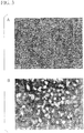
- Tables 1 and 2 Conditions and results of evaluation are shown in Tables 1 and 2. As examples of the above-described observation of microstructures, SEM observation photographs of the Inventive Example 12 and Inventive Example 39 are shown in FIG. 2 and FIG. 3 . In FIG. 2 and FIG. 3 , A shows an area at 10000 fold magnification and B shows an area at 50000 fold magnification.
- Comparative Examples 1, 2 having a smaller Mg content and a smaller Al content than the ranges of the present invention showed a high Young's modulus of 127 GPa and 126 GPa.
- Comparative Example 3 having a larger Mg content than the range of the present invention and Comparative Example 4 having a larger Al content than the range of the present invention showed occurrence of large edge cracking in the time of cold rolling. As a result, it was impossible to examine their properties.
- the Young's modulus was controlled to be low value of 120GPa or less showing excellent elasticity in each of Inventive Examples (Examples according to the present invention) 1-39.
- the Examples according to the present invention could provide a copper alloy for an electronic device that had a low Young's modulus, a high yield strength, and high electrical conductivity, and that was appropriately applicable to electronic/electric devices such as terminals, connectors, relays or the like.
- the present invention it is possible to provide copper alloy for an electronic device that has low Young's modulus, high Yield strength, high electrical conductivity, and that is appropriately applicable to electronic/electric components such as terminals, connectors, and relays, and to provide a method of producing a copper alloy for an electronic device, and a copper alloy rolled material for an electronic device.
Landscapes
- Chemical & Material Sciences (AREA)
- Engineering & Computer Science (AREA)
- Materials Engineering (AREA)
- Mechanical Engineering (AREA)
- Metallurgy (AREA)
- Organic Chemistry (AREA)
- Physics & Mathematics (AREA)
- Thermal Sciences (AREA)
- Crystallography & Structural Chemistry (AREA)
- Conductive Materials (AREA)
- Non-Insulated Conductors (AREA)
Applications Claiming Priority (2)
| Application Number | Priority Date | Filing Date | Title |
|---|---|---|---|
| JP2010112267A JP5045784B2 (ja) | 2010-05-14 | 2010-05-14 | 電子機器用銅合金、電子機器用銅合金の製造方法及び電子機器用銅合金圧延材 |
| PCT/JP2011/060962 WO2011142428A1 (ja) | 2010-05-14 | 2011-05-12 | 電子機器用銅合金、電子機器用銅合金の製造方法及び電子機器用銅合金圧延材 |
Publications (3)
| Publication Number | Publication Date |
|---|---|
| EP2570505A1 EP2570505A1 (en) | 2013-03-20 |
| EP2570505A4 EP2570505A4 (en) | 2014-08-06 |
| EP2570505B1 true EP2570505B1 (en) | 2016-12-28 |
Family
ID=44914480
Family Applications (1)
| Application Number | Title | Priority Date | Filing Date |
|---|---|---|---|
| EP11780685.1A Active EP2570505B1 (en) | 2010-05-14 | 2011-05-12 | Copper alloy and copper alloy rolled material for electronic device and method for producing this alloy |
Country Status (7)
| Country | Link |
|---|---|
| US (1) | US20130056116A1 (enExample) |
| EP (1) | EP2570505B1 (enExample) |
| JP (1) | JP5045784B2 (enExample) |
| KR (1) | KR101477884B1 (enExample) |
| CN (1) | CN102892908B (enExample) |
| TW (1) | TWI503425B (enExample) |
| WO (1) | WO2011142428A1 (enExample) |
Families Citing this family (28)
| Publication number | Priority date | Publication date | Assignee | Title |
|---|---|---|---|---|
| JP5712585B2 (ja) * | 2010-12-03 | 2015-05-07 | 三菱マテリアル株式会社 | 電子機器用銅合金、電子機器用銅合金の製造方法及び電子機器用銅合金圧延材 |
| JP6248387B2 (ja) * | 2012-12-05 | 2017-12-20 | 三菱マテリアル株式会社 | 電子・電気機器用銅合金、電子・電気機器用部品及び端子 |
| JP6248389B2 (ja) * | 2012-12-05 | 2017-12-20 | 三菱マテリアル株式会社 | 電子・電気機器用銅合金、電子・電気機器用部品及び端子 |
| JP6248388B2 (ja) * | 2012-12-05 | 2017-12-20 | 三菱マテリアル株式会社 | 電子・電気機器用銅合金、電子・電気機器用部品及び端子 |
| JP6248386B2 (ja) * | 2012-12-05 | 2017-12-20 | 三菱マテリアル株式会社 | 電子・電気機器用銅合金、電子・電気機器用部品及び端子 |
| JP5962707B2 (ja) * | 2013-07-31 | 2016-08-03 | 三菱マテリアル株式会社 | 電子・電気機器用銅合金、電子・電気機器用銅合金塑性加工材、電子・電気機器用銅合金塑性加工材の製造方法、電子・電気機器用部品及び端子 |
| JP5668814B1 (ja) * | 2013-08-12 | 2015-02-12 | 三菱マテリアル株式会社 | 電子・電気機器用銅合金、電子・電気機器用銅合金薄板、電子・電気機器用部品、端子およびバスバー |
| JP5983589B2 (ja) | 2013-12-11 | 2016-08-31 | 三菱マテリアル株式会社 | 電子・電気機器用銅合金圧延材、電子・電気機器用部品及び端子 |
| CN103695704A (zh) * | 2013-12-26 | 2014-04-02 | 青岛友铭辰生物技术有限公司 | 一种电气电子设备用耐疲劳铜合金材料及其制备方法 |
| CN104051080B (zh) * | 2014-07-03 | 2016-06-15 | 深圳市凯中和东新材料有限公司 | 绝缘性导线的制备方法 |
| CN104100950B (zh) * | 2014-08-05 | 2017-01-18 | 东莞市闻誉实业有限公司 | 组装式的散热器 |
| CN106834788A (zh) * | 2015-12-03 | 2017-06-13 | 黄波 | 一种含钐元素抗拉伸铜合金导线及其制备方法 |
| CN106834787A (zh) * | 2015-12-03 | 2017-06-13 | 黄波 | 一种Gu-Pm-Au-B合金导线及其制备方法 |
| CN106834785A (zh) * | 2015-12-03 | 2017-06-13 | 黄波 | 一种Gu-Nd-Au-B合金导线及其制备方法 |
| CN106834790A (zh) * | 2015-12-03 | 2017-06-13 | 黄波 | 一种Gu-Gd-Au-B合金导线及其制备方法 |
| CN106834789A (zh) * | 2015-12-03 | 2017-06-13 | 黄波 | 一种Gu-Ce-Au-B合金导线及其制备方法 |
| CN105463237B (zh) * | 2015-12-05 | 2017-12-01 | 烟台一诺电子材料有限公司 | 一种铜银合金键合丝及其制备方法 |
| CN105506349A (zh) * | 2015-12-22 | 2016-04-20 | 江苏艾克斯展示器材有限公司 | 展示架 |
| CN105506366A (zh) * | 2015-12-24 | 2016-04-20 | 常熟市易安达电器有限公司 | 矿用扇形喷雾杆 |
| CN105506354A (zh) * | 2015-12-25 | 2016-04-20 | 苏州露宇电子科技有限公司 | 核磁共振成像装置 |
| CN105568043A (zh) * | 2016-02-03 | 2016-05-11 | 安徽华联电缆集团有限公司 | 一种钪合金高性能电缆 |
| FI3438299T3 (fi) | 2016-03-30 | 2023-05-23 | Mitsubishi Materials Corp | Kupariseoksesta valmistettu nauha elektronisia laitteita ja sähkölaitteita varten, komponentti, liitosnapa, virtakisko sekä liikuteltava kappale releitä varten |
| WO2017170699A1 (ja) | 2016-03-30 | 2017-10-05 | 三菱マテリアル株式会社 | 電子・電気機器用銅合金、電子・電気機器用銅合金板条材、電子・電気機器用部品、端子、バスバー、及び、リレー用可動片 |
| CN106222482A (zh) * | 2016-08-29 | 2016-12-14 | 芜湖楚江合金铜材有限公司 | 一种抗拉性能良好的高强度铜线及其制备方法 |
| DE112018001576T5 (de) * | 2017-03-24 | 2019-12-19 | Ihi Corporation | Verschleißfeste Kupfer-Zink-Legierung und mechanische Vorrichtung, die sie verwendet |
| JP6780187B2 (ja) | 2018-03-30 | 2020-11-04 | 三菱マテリアル株式会社 | 電子・電気機器用銅合金、電子・電気機器用銅合金板条材、電子・電気機器用部品、端子、及び、バスバー |
| CN111788320B (zh) | 2018-03-30 | 2022-01-14 | 三菱综合材料株式会社 | 电子电气设备用铜合金﹑电子电气设备用铜合金板条材、电子电气设备用组件、端子及汇流排 |
| CN112593115A (zh) * | 2020-12-21 | 2021-04-02 | 杭州昶海电力科技有限公司 | 一种高压开关触片加工工艺 |
Family Cites Families (19)
| Publication number | Priority date | Publication date | Assignee | Title |
|---|---|---|---|---|
| JPS5675541A (en) * | 1979-11-22 | 1981-06-22 | Sumitomo Light Metal Ind Ltd | Copper alloy for water or hot water supply piping material and heat exchanger tube material |
| JPS62227051A (ja) | 1986-03-28 | 1987-10-06 | Mitsubishi Shindo Kk | Cu合金製電気機器用コネクタ |
| JPH04268033A (ja) | 1991-02-21 | 1992-09-24 | Ngk Insulators Ltd | ベリリウム銅合金の製造方法 |
| JPH059619A (ja) * | 1991-07-08 | 1993-01-19 | Furukawa Electric Co Ltd:The | 高力銅合金の製造方法 |
| JP3796784B2 (ja) * | 1995-12-01 | 2006-07-12 | 三菱伸銅株式会社 | コネクタ製造用銅合金薄板およびその薄板で製造したコネクタ |
| JP3465541B2 (ja) | 1997-07-16 | 2003-11-10 | 日立電線株式会社 | リードフレーム材の製造方法 |
| CN1062608C (zh) * | 1998-02-13 | 2001-02-28 | 北京有色金属研究总院 | 一种用于冷阴极材料的铜合金及其制法 |
| SE525460C2 (sv) * | 2002-02-28 | 2005-02-22 | Sandvik Ab | Användning av en kopparlegering i uppkolande miljöer |
| JP4787986B2 (ja) * | 2002-11-25 | 2011-10-05 | Dowaメタルテック株式会社 | 銅合金およびその製造方法 |
| EP1803829B1 (en) * | 2004-08-17 | 2013-05-22 | Kabushiki Kaisha Kobe Seiko Sho | Copper alloy plate for electric and electronic parts having bendability |
| DE602006002573D1 (de) * | 2005-09-09 | 2008-10-16 | Ngk Insulators Ltd | Kupfer Legierungblech mit Nickel und Beryllium und Verfahren zur Herstellung derselben |
| CN100462458C (zh) * | 2006-10-30 | 2009-02-18 | 西安交通大学 | 熔体快淬铜铬钛锆钴触头材料 |
| EP2154257B1 (en) * | 2007-03-30 | 2016-10-05 | JX Nippon Mining & Metals Corporation | Cu-ni-si-based alloy for electronic material |
| EP2248921A4 (en) * | 2008-01-31 | 2011-03-16 | Furukawa Electric Co Ltd | COPPER ALLOY MATERIAL FOR ELECTRICAL / ELECTRONIC COMPONENT AND METHOD FOR PRODUCING THE COPPER ALLOY MATERIAL |
| JP5260992B2 (ja) * | 2008-03-19 | 2013-08-14 | Dowaメタルテック株式会社 | 銅合金板材およびその製造方法 |
| JP5420328B2 (ja) * | 2008-08-01 | 2014-02-19 | 三菱マテリアル株式会社 | フラットパネルディスプレイ用配線膜形成用スパッタリングターゲット |
| CN101487091A (zh) * | 2009-02-25 | 2009-07-22 | 中南大学 | 一种无铅易切削镁硅黄铜 |
| JP5712585B2 (ja) * | 2010-12-03 | 2015-05-07 | 三菱マテリアル株式会社 | 電子機器用銅合金、電子機器用銅合金の製造方法及び電子機器用銅合金圧延材 |
| JP5903842B2 (ja) * | 2011-11-14 | 2016-04-13 | 三菱マテリアル株式会社 | 銅合金、銅合金塑性加工材及び銅合金塑性加工材の製造方法 |
-
2010
- 2010-05-14 JP JP2010112267A patent/JP5045784B2/ja not_active Expired - Fee Related
-
2011
- 2011-05-12 WO PCT/JP2011/060962 patent/WO2011142428A1/ja not_active Ceased
- 2011-05-12 US US13/697,441 patent/US20130056116A1/en not_active Abandoned
- 2011-05-12 EP EP11780685.1A patent/EP2570505B1/en active Active
- 2011-05-12 KR KR1020127030659A patent/KR101477884B1/ko active Active
- 2011-05-12 CN CN201180023685.6A patent/CN102892908B/zh active Active
- 2011-05-13 TW TW100116852A patent/TWI503425B/zh active
Non-Patent Citations (1)
| Title |
|---|
| None * |
Also Published As
| Publication number | Publication date |
|---|---|
| WO2011142428A1 (ja) | 2011-11-17 |
| EP2570505A4 (en) | 2014-08-06 |
| CN102892908B (zh) | 2015-07-01 |
| US20130056116A1 (en) | 2013-03-07 |
| TW201213562A (en) | 2012-04-01 |
| TWI503425B (zh) | 2015-10-11 |
| EP2570505A1 (en) | 2013-03-20 |
| JP2011241413A (ja) | 2011-12-01 |
| JP5045784B2 (ja) | 2012-10-10 |
| CN102892908A (zh) | 2013-01-23 |
| KR20130010018A (ko) | 2013-01-24 |
| KR101477884B1 (ko) | 2014-12-30 |
Similar Documents
| Publication | Publication Date | Title |
|---|---|---|
| EP2570505B1 (en) | Copper alloy and copper alloy rolled material for electronic device and method for producing this alloy | |
| TWI591191B (zh) | 電子機器用銅合金、電子機器用銅合金的製造方法及電子機器用銅合金輥軋材 | |
| KR101615830B1 (ko) | 전자 기기용 구리 합금, 전자 기기용 구리 합금의 제조 방법, 전자 기기용 구리 합금 소성 가공재 및 전자 기기용 부품 | |
| EP2570506B1 (en) | Copper alloy for electronic device, method for producing this alloy, and copper alloy rolled material for this device | |
| US10294547B2 (en) | Copper alloy for electronic and electrical equipment, plastically worked copper alloy material for electronic and electrical equipment, and component and terminal for electronic and electrical equipment | |
| KR101554833B1 (ko) | 전자 기기용 구리 합금, 전자 기기용 구리 합금의 제조 방법, 전자 기기용 구리 합금 압연재 및 전자 기기용 부품 | |
| TWI513833B (zh) | 電子機器用銅合金、電子機器用銅合金之製造方法、電子機器銅合金用塑性加工材、以及電子機器用零件 | |
| TWI429764B (zh) | Cu-Co-Si alloy for electronic materials | |
| JP2011241412A (ja) | 電子機器用銅合金、電子機器用銅合金の製造方法及び電子機器用銅合金圧延材 | |
| WO2010126046A1 (ja) | 導電性と曲げ性を改善したCu-Ni-Si-Mg系合金 | |
| JP2013100571A (ja) | 電子機器用銅合金、電子機器用銅合金の製造方法、電子機器用銅合金塑性加工材および電子機器用部品 | |
| JP5045782B2 (ja) | 電子機器用銅合金、電子機器用銅合金の製造方法及び電子機器用銅合金圧延材 |
Legal Events
| Date | Code | Title | Description |
|---|---|---|---|
| PUAI | Public reference made under article 153(3) epc to a published international application that has entered the european phase |
Free format text: ORIGINAL CODE: 0009012 |
|
| 17P | Request for examination filed |
Effective date: 20121123 |
|
| AK | Designated contracting states |
Kind code of ref document: A1 Designated state(s): AL AT BE BG CH CY CZ DE DK EE ES FI FR GB GR HR HU IE IS IT LI LT LU LV MC MK MT NL NO PL PT RO RS SE SI SK SM TR |
|
| DAX | Request for extension of the european patent (deleted) | ||
| RIC1 | Information provided on ipc code assigned before grant |
Ipc: C22C 9/00 20060101AFI20140528BHEP Ipc: H01B 5/02 20060101ALI20140528BHEP Ipc: C22C 9/04 20060101ALI20140528BHEP Ipc: C22C 9/01 20060101ALI20140528BHEP Ipc: C22F 1/08 20060101ALI20140528BHEP Ipc: H01B 13/00 20060101ALI20140528BHEP Ipc: H01B 1/02 20060101ALI20140528BHEP Ipc: H01R 13/03 20060101ALI20140528BHEP |
|
| RIC1 | Information provided on ipc code assigned before grant |
Ipc: H01B 13/00 20060101ALI20140626BHEP Ipc: H01R 13/03 20060101ALI20140626BHEP Ipc: C22C 9/01 20060101ALI20140626BHEP Ipc: H01B 5/02 20060101ALI20140626BHEP Ipc: H01B 1/02 20060101ALI20140626BHEP Ipc: C22C 9/00 20060101AFI20140626BHEP Ipc: C22F 1/08 20060101ALI20140626BHEP Ipc: C22C 9/04 20060101ALI20140626BHEP |
|
| A4 | Supplementary search report drawn up and despatched |
Effective date: 20140704 |
|
| 17Q | First examination report despatched |
Effective date: 20150305 |
|
| GRAP | Despatch of communication of intention to grant a patent |
Free format text: ORIGINAL CODE: EPIDOSNIGR1 |
|
| RIC1 | Information provided on ipc code assigned before grant |
Ipc: H01B 1/02 20060101ALI20160622BHEP Ipc: C22C 9/00 20060101AFI20160622BHEP Ipc: C22C 1/02 20060101ALI20160622BHEP Ipc: H01B 13/00 20060101ALI20160622BHEP Ipc: H01B 5/02 20060101ALI20160622BHEP Ipc: C22C 9/01 20060101ALI20160622BHEP Ipc: C22C 9/04 20060101ALI20160622BHEP Ipc: C22F 1/08 20060101ALI20160622BHEP Ipc: H01R 13/03 20060101ALI20160622BHEP |
|
| INTG | Intention to grant announced |
Effective date: 20160713 |
|
| GRAS | Grant fee paid |
Free format text: ORIGINAL CODE: EPIDOSNIGR3 |
|
| GRAA | (expected) grant |
Free format text: ORIGINAL CODE: 0009210 |
|
| AK | Designated contracting states |
Kind code of ref document: B1 Designated state(s): AL AT BE BG CH CY CZ DE DK EE ES FI FR GB GR HR HU IE IS IT LI LT LU LV MC MK MT NL NO PL PT RO RS SE SI SK SM TR |
|
| REG | Reference to a national code |
Ref country code: GB Ref legal event code: FG4D |
|
| REG | Reference to a national code |
Ref country code: CH Ref legal event code: EP |
|
| REG | Reference to a national code |
Ref country code: AT Ref legal event code: REF Ref document number: 857356 Country of ref document: AT Kind code of ref document: T Effective date: 20170115 |
|
| REG | Reference to a national code |
Ref country code: IE Ref legal event code: FG4D |
|
| REG | Reference to a national code |
Ref country code: DE Ref legal event code: R096 Ref document number: 602011033880 Country of ref document: DE |
|
| PG25 | Lapsed in a contracting state [announced via postgrant information from national office to epo] |
Ref country code: LV Free format text: LAPSE BECAUSE OF FAILURE TO SUBMIT A TRANSLATION OF THE DESCRIPTION OR TO PAY THE FEE WITHIN THE PRESCRIBED TIME-LIMIT Effective date: 20161228 |
|
| REG | Reference to a national code |
Ref country code: LT Ref legal event code: MG4D |
|
| PG25 | Lapsed in a contracting state [announced via postgrant information from national office to epo] |
Ref country code: SE Free format text: LAPSE BECAUSE OF FAILURE TO SUBMIT A TRANSLATION OF THE DESCRIPTION OR TO PAY THE FEE WITHIN THE PRESCRIBED TIME-LIMIT Effective date: 20161228 Ref country code: NO Free format text: LAPSE BECAUSE OF FAILURE TO SUBMIT A TRANSLATION OF THE DESCRIPTION OR TO PAY THE FEE WITHIN THE PRESCRIBED TIME-LIMIT Effective date: 20170328 Ref country code: GR Free format text: LAPSE BECAUSE OF FAILURE TO SUBMIT A TRANSLATION OF THE DESCRIPTION OR TO PAY THE FEE WITHIN THE PRESCRIBED TIME-LIMIT Effective date: 20170329 Ref country code: LT Free format text: LAPSE BECAUSE OF FAILURE TO SUBMIT A TRANSLATION OF THE DESCRIPTION OR TO PAY THE FEE WITHIN THE PRESCRIBED TIME-LIMIT Effective date: 20161228 |
|
| REG | Reference to a national code |
Ref country code: NL Ref legal event code: MP Effective date: 20161228 |
|
| REG | Reference to a national code |
Ref country code: AT Ref legal event code: MK05 Ref document number: 857356 Country of ref document: AT Kind code of ref document: T Effective date: 20161228 |
|
| PG25 | Lapsed in a contracting state [announced via postgrant information from national office to epo] |
Ref country code: RS Free format text: LAPSE BECAUSE OF FAILURE TO SUBMIT A TRANSLATION OF THE DESCRIPTION OR TO PAY THE FEE WITHIN THE PRESCRIBED TIME-LIMIT Effective date: 20161228 Ref country code: HR Free format text: LAPSE BECAUSE OF FAILURE TO SUBMIT A TRANSLATION OF THE DESCRIPTION OR TO PAY THE FEE WITHIN THE PRESCRIBED TIME-LIMIT Effective date: 20161228 Ref country code: FI Free format text: LAPSE BECAUSE OF FAILURE TO SUBMIT A TRANSLATION OF THE DESCRIPTION OR TO PAY THE FEE WITHIN THE PRESCRIBED TIME-LIMIT Effective date: 20161228 |
|
| PG25 | Lapsed in a contracting state [announced via postgrant information from national office to epo] |
Ref country code: NL Free format text: LAPSE BECAUSE OF FAILURE TO SUBMIT A TRANSLATION OF THE DESCRIPTION OR TO PAY THE FEE WITHIN THE PRESCRIBED TIME-LIMIT Effective date: 20161228 |
|
| PG25 | Lapsed in a contracting state [announced via postgrant information from national office to epo] |
Ref country code: SK Free format text: LAPSE BECAUSE OF FAILURE TO SUBMIT A TRANSLATION OF THE DESCRIPTION OR TO PAY THE FEE WITHIN THE PRESCRIBED TIME-LIMIT Effective date: 20161228 Ref country code: IS Free format text: LAPSE BECAUSE OF FAILURE TO SUBMIT A TRANSLATION OF THE DESCRIPTION OR TO PAY THE FEE WITHIN THE PRESCRIBED TIME-LIMIT Effective date: 20170428 Ref country code: EE Free format text: LAPSE BECAUSE OF FAILURE TO SUBMIT A TRANSLATION OF THE DESCRIPTION OR TO PAY THE FEE WITHIN THE PRESCRIBED TIME-LIMIT Effective date: 20161228 Ref country code: CZ Free format text: LAPSE BECAUSE OF FAILURE TO SUBMIT A TRANSLATION OF THE DESCRIPTION OR TO PAY THE FEE WITHIN THE PRESCRIBED TIME-LIMIT Effective date: 20161228 Ref country code: RO Free format text: LAPSE BECAUSE OF FAILURE TO SUBMIT A TRANSLATION OF THE DESCRIPTION OR TO PAY THE FEE WITHIN THE PRESCRIBED TIME-LIMIT Effective date: 20161228 |
|
| PG25 | Lapsed in a contracting state [announced via postgrant information from national office to epo] |
Ref country code: IT Free format text: LAPSE BECAUSE OF FAILURE TO SUBMIT A TRANSLATION OF THE DESCRIPTION OR TO PAY THE FEE WITHIN THE PRESCRIBED TIME-LIMIT Effective date: 20161228 Ref country code: BE Free format text: LAPSE BECAUSE OF FAILURE TO SUBMIT A TRANSLATION OF THE DESCRIPTION OR TO PAY THE FEE WITHIN THE PRESCRIBED TIME-LIMIT Effective date: 20161228 Ref country code: PL Free format text: LAPSE BECAUSE OF FAILURE TO SUBMIT A TRANSLATION OF THE DESCRIPTION OR TO PAY THE FEE WITHIN THE PRESCRIBED TIME-LIMIT Effective date: 20161228 Ref country code: ES Free format text: LAPSE BECAUSE OF FAILURE TO SUBMIT A TRANSLATION OF THE DESCRIPTION OR TO PAY THE FEE WITHIN THE PRESCRIBED TIME-LIMIT Effective date: 20161228 Ref country code: PT Free format text: LAPSE BECAUSE OF FAILURE TO SUBMIT A TRANSLATION OF THE DESCRIPTION OR TO PAY THE FEE WITHIN THE PRESCRIBED TIME-LIMIT Effective date: 20170428 Ref country code: BG Free format text: LAPSE BECAUSE OF FAILURE TO SUBMIT A TRANSLATION OF THE DESCRIPTION OR TO PAY THE FEE WITHIN THE PRESCRIBED TIME-LIMIT Effective date: 20170328 Ref country code: SM Free format text: LAPSE BECAUSE OF FAILURE TO SUBMIT A TRANSLATION OF THE DESCRIPTION OR TO PAY THE FEE WITHIN THE PRESCRIBED TIME-LIMIT Effective date: 20161228 Ref country code: LU Free format text: LAPSE BECAUSE OF NON-PAYMENT OF DUE FEES Effective date: 20170531 Ref country code: AT Free format text: LAPSE BECAUSE OF FAILURE TO SUBMIT A TRANSLATION OF THE DESCRIPTION OR TO PAY THE FEE WITHIN THE PRESCRIBED TIME-LIMIT Effective date: 20161228 |
|
| REG | Reference to a national code |
Ref country code: DE Ref legal event code: R097 Ref document number: 602011033880 Country of ref document: DE |
|
| PLBE | No opposition filed within time limit |
Free format text: ORIGINAL CODE: 0009261 |
|
| STAA | Information on the status of an ep patent application or granted ep patent |
Free format text: STATUS: NO OPPOSITION FILED WITHIN TIME LIMIT |
|
| PG25 | Lapsed in a contracting state [announced via postgrant information from national office to epo] |
Ref country code: DK Free format text: LAPSE BECAUSE OF FAILURE TO SUBMIT A TRANSLATION OF THE DESCRIPTION OR TO PAY THE FEE WITHIN THE PRESCRIBED TIME-LIMIT Effective date: 20161228 |
|
| 26N | No opposition filed |
Effective date: 20170929 |
|
| REG | Reference to a national code |
Ref country code: CH Ref legal event code: PL |
|
| GBPC | Gb: european patent ceased through non-payment of renewal fee |
Effective date: 20170512 |
|
| PG25 | Lapsed in a contracting state [announced via postgrant information from national office to epo] |
Ref country code: MC Free format text: LAPSE BECAUSE OF FAILURE TO SUBMIT A TRANSLATION OF THE DESCRIPTION OR TO PAY THE FEE WITHIN THE PRESCRIBED TIME-LIMIT Effective date: 20161228 |
|
| REG | Reference to a national code |
Ref country code: IE Ref legal event code: MM4A |
|
| PG25 | Lapsed in a contracting state [announced via postgrant information from national office to epo] |
Ref country code: LI Free format text: LAPSE BECAUSE OF NON-PAYMENT OF DUE FEES Effective date: 20170531 Ref country code: SI Free format text: LAPSE BECAUSE OF FAILURE TO SUBMIT A TRANSLATION OF THE DESCRIPTION OR TO PAY THE FEE WITHIN THE PRESCRIBED TIME-LIMIT Effective date: 20161228 Ref country code: CH Free format text: LAPSE BECAUSE OF NON-PAYMENT OF DUE FEES Effective date: 20170531 |
|
| REG | Reference to a national code |
Ref country code: FR Ref legal event code: ST Effective date: 20180131 |
|
| PG25 | Lapsed in a contracting state [announced via postgrant information from national office to epo] |
Ref country code: LU Free format text: LAPSE BECAUSE OF NON-PAYMENT OF DUE FEES Effective date: 20170512 |
|
| PG25 | Lapsed in a contracting state [announced via postgrant information from national office to epo] |
Ref country code: IE Free format text: LAPSE BECAUSE OF NON-PAYMENT OF DUE FEES Effective date: 20170512 Ref country code: GB Free format text: LAPSE BECAUSE OF NON-PAYMENT OF DUE FEES Effective date: 20170512 |
|
| PG25 | Lapsed in a contracting state [announced via postgrant information from national office to epo] |
Ref country code: FR Free format text: LAPSE BECAUSE OF NON-PAYMENT OF DUE FEES Effective date: 20170531 |
|
| PG25 | Lapsed in a contracting state [announced via postgrant information from national office to epo] |
Ref country code: MT Free format text: LAPSE BECAUSE OF NON-PAYMENT OF DUE FEES Effective date: 20170512 |
|
| PG25 | Lapsed in a contracting state [announced via postgrant information from national office to epo] |
Ref country code: HU Free format text: LAPSE BECAUSE OF FAILURE TO SUBMIT A TRANSLATION OF THE DESCRIPTION OR TO PAY THE FEE WITHIN THE PRESCRIBED TIME-LIMIT; INVALID AB INITIO Effective date: 20110512 |
|
| PG25 | Lapsed in a contracting state [announced via postgrant information from national office to epo] |
Ref country code: CY Free format text: LAPSE BECAUSE OF NON-PAYMENT OF DUE FEES Effective date: 20161228 |
|
| PG25 | Lapsed in a contracting state [announced via postgrant information from national office to epo] |
Ref country code: MK Free format text: LAPSE BECAUSE OF FAILURE TO SUBMIT A TRANSLATION OF THE DESCRIPTION OR TO PAY THE FEE WITHIN THE PRESCRIBED TIME-LIMIT Effective date: 20161228 |
|
| PG25 | Lapsed in a contracting state [announced via postgrant information from national office to epo] |
Ref country code: TR Free format text: LAPSE BECAUSE OF FAILURE TO SUBMIT A TRANSLATION OF THE DESCRIPTION OR TO PAY THE FEE WITHIN THE PRESCRIBED TIME-LIMIT Effective date: 20161228 |
|
| PG25 | Lapsed in a contracting state [announced via postgrant information from national office to epo] |
Ref country code: AL Free format text: LAPSE BECAUSE OF FAILURE TO SUBMIT A TRANSLATION OF THE DESCRIPTION OR TO PAY THE FEE WITHIN THE PRESCRIBED TIME-LIMIT Effective date: 20161228 |
|
| PGFP | Annual fee paid to national office [announced via postgrant information from national office to epo] |
Ref country code: DE Payment date: 20250521 Year of fee payment: 15 |