EP2553684B1 - Erfassungsschaltung mit selektiven/differentiellen schwellenspannungsfunktionen - Google Patents
Erfassungsschaltung mit selektiven/differentiellen schwellenspannungsfunktionen Download PDFInfo
- Publication number
- EP2553684B1 EP2553684B1 EP11763403.0A EP11763403A EP2553684B1 EP 2553684 B1 EP2553684 B1 EP 2553684B1 EP 11763403 A EP11763403 A EP 11763403A EP 2553684 B1 EP2553684 B1 EP 2553684B1
- Authority
- EP
- European Patent Office
- Prior art keywords
- region
- threshold voltage
- insulating portion
- threshold
- transistor
- Prior art date
- Legal status (The legal status is an assumption and is not a legal conclusion. Google has not performed a legal analysis and makes no representation as to the accuracy of the status listed.)
- Active
Links
Images





Classifications
-
- G—PHYSICS
- G11—INFORMATION STORAGE
- G11C—STATIC STORES
- G11C7/00—Arrangements for writing information into, or reading information out from, a digital store
- G11C7/06—Sense amplifiers; Associated circuits, e.g. timing or triggering circuits
- G11C7/062—Differential amplifiers of non-latching type, e.g. comparators, long-tailed pairs
-
- G—PHYSICS
- G11—INFORMATION STORAGE
- G11C—STATIC STORES
- G11C7/00—Arrangements for writing information into, or reading information out from, a digital store
- G11C7/06—Sense amplifiers; Associated circuits, e.g. timing or triggering circuits
- G11C7/065—Differential amplifiers of latching type
-
- G—PHYSICS
- G11—INFORMATION STORAGE
- G11C—STATIC STORES
- G11C16/00—Erasable programmable read-only memories
- G11C16/02—Erasable programmable read-only memories electrically programmable
- G11C16/06—Auxiliary circuits, e.g. for writing into memory
-
- G—PHYSICS
- G11—INFORMATION STORAGE
- G11C—STATIC STORES
- G11C11/00—Digital stores characterised by the use of particular electric or magnetic storage elements; Storage elements therefor
- G11C11/21—Digital stores characterised by the use of particular electric or magnetic storage elements; Storage elements therefor using electric elements
- G11C11/34—Digital stores characterised by the use of particular electric or magnetic storage elements; Storage elements therefor using electric elements using semiconductor devices
-
- G—PHYSICS
- G11—INFORMATION STORAGE
- G11C—STATIC STORES
- G11C16/00—Erasable programmable read-only memories
- G11C16/02—Erasable programmable read-only memories electrically programmable
- G11C16/06—Auxiliary circuits, e.g. for writing into memory
- G11C16/26—Sensing or reading circuits; Data output circuits
- G11C16/28—Sensing or reading circuits; Data output circuits using differential sensing or reference cells, e.g. dummy cells
-
- G—PHYSICS
- G11—INFORMATION STORAGE
- G11C—STATIC STORES
- G11C7/00—Arrangements for writing information into, or reading information out from, a digital store
- G11C7/06—Sense amplifiers; Associated circuits, e.g. timing or triggering circuits
-
- H—ELECTRICITY
- H10—SEMICONDUCTOR DEVICES; ELECTRIC SOLID-STATE DEVICES NOT OTHERWISE PROVIDED FOR
- H10D—INORGANIC ELECTRIC SEMICONDUCTOR DEVICES
- H10D30/00—Field-effect transistors [FET]
- H10D30/01—Manufacture or treatment
- H10D30/021—Manufacture or treatment of FETs having insulated gates [IGFET]
- H10D30/0413—Manufacture or treatment of FETs having insulated gates [IGFET] of FETs having charge-trapping gate insulators, e.g. MNOS transistors
-
- H—ELECTRICITY
- H10—SEMICONDUCTOR DEVICES; ELECTRIC SOLID-STATE DEVICES NOT OTHERWISE PROVIDED FOR
- H10D—INORGANIC ELECTRIC SEMICONDUCTOR DEVICES
- H10D30/00—Field-effect transistors [FET]
- H10D30/60—Insulated-gate field-effect transistors [IGFET]
- H10D30/601—Insulated-gate field-effect transistors [IGFET] having lightly-doped drain or source extensions, e.g. LDD IGFETs or DDD IGFETs
- H10D30/603—Insulated-gate field-effect transistors [IGFET] having lightly-doped drain or source extensions, e.g. LDD IGFETs or DDD IGFETs having asymmetry in the channel direction, e.g. lateral high-voltage MISFETs having drain offset region or extended drain IGFETs [EDMOS]
-
- H—ELECTRICITY
- H10—SEMICONDUCTOR DEVICES; ELECTRIC SOLID-STATE DEVICES NOT OTHERWISE PROVIDED FOR
- H10D—INORGANIC ELECTRIC SEMICONDUCTOR DEVICES
- H10D30/00—Field-effect transistors [FET]
- H10D30/60—Insulated-gate field-effect transistors [IGFET]
- H10D30/69—IGFETs having charge trapping gate insulators, e.g. MNOS transistors
-
- H—ELECTRICITY
- H10—SEMICONDUCTOR DEVICES; ELECTRIC SOLID-STATE DEVICES NOT OTHERWISE PROVIDED FOR
- H10D—INORGANIC ELECTRIC SEMICONDUCTOR DEVICES
- H10D62/00—Semiconductor bodies, or regions thereof, of devices having potential barriers
- H10D62/10—Shapes, relative sizes or dispositions of the regions of the semiconductor bodies; Shapes of the semiconductor bodies
- H10D62/17—Semiconductor regions connected to electrodes not carrying current to be rectified, amplified or switched, e.g. channel regions
- H10D62/351—Substrate regions of field-effect devices
- H10D62/357—Substrate regions of field-effect devices of FETs
- H10D62/364—Substrate regions of field-effect devices of FETs of IGFETs
- H10D62/371—Inactive supplementary semiconductor regions, e.g. for preventing punch-through, improving capacity effect or leakage current
-
- H—ELECTRICITY
- H10—SEMICONDUCTOR DEVICES; ELECTRIC SOLID-STATE DEVICES NOT OTHERWISE PROVIDED FOR
- H10D—INORGANIC ELECTRIC SEMICONDUCTOR DEVICES
- H10D64/00—Electrodes of devices having potential barriers
- H10D64/01—Manufacture or treatment
- H10D64/031—Manufacture or treatment of data-storage electrodes
- H10D64/037—Manufacture or treatment of data-storage electrodes comprising charge-trapping insulators
-
- H—ELECTRICITY
- H10—SEMICONDUCTOR DEVICES; ELECTRIC SOLID-STATE DEVICES NOT OTHERWISE PROVIDED FOR
- H10D—INORGANIC ELECTRIC SEMICONDUCTOR DEVICES
- H10D64/00—Electrodes of devices having potential barriers
- H10D64/20—Electrodes characterised by their shapes, relative sizes or dispositions
- H10D64/27—Electrodes not carrying the current to be rectified, amplified, oscillated or switched, e.g. gates
- H10D64/311—Gate electrodes for field-effect devices
- H10D64/411—Gate electrodes for field-effect devices for FETs
- H10D64/511—Gate electrodes for field-effect devices for FETs for IGFETs
- H10D64/514—Gate electrodes for field-effect devices for FETs for IGFETs characterised by the insulating layers
- H10D64/516—Gate electrodes for field-effect devices for FETs for IGFETs characterised by the insulating layers the thicknesses being non-uniform
-
- H—ELECTRICITY
- H10—SEMICONDUCTOR DEVICES; ELECTRIC SOLID-STATE DEVICES NOT OTHERWISE PROVIDED FOR
- H10D—INORGANIC ELECTRIC SEMICONDUCTOR DEVICES
- H10D64/00—Electrodes of devices having potential barriers
- H10D64/20—Electrodes characterised by their shapes, relative sizes or dispositions
- H10D64/27—Electrodes not carrying the current to be rectified, amplified, oscillated or switched, e.g. gates
- H10D64/311—Gate electrodes for field-effect devices
- H10D64/411—Gate electrodes for field-effect devices for FETs
- H10D64/511—Gate electrodes for field-effect devices for FETs for IGFETs
- H10D64/517—Gate electrodes for field-effect devices for FETs for IGFETs characterised by the conducting layers
- H10D64/519—Gate electrodes for field-effect devices for FETs for IGFETs characterised by the conducting layers characterised by their top-view geometrical layouts
-
- H—ELECTRICITY
- H10—SEMICONDUCTOR DEVICES; ELECTRIC SOLID-STATE DEVICES NOT OTHERWISE PROVIDED FOR
- H10D—INORGANIC ELECTRIC SEMICONDUCTOR DEVICES
- H10D84/00—Integrated devices formed in or on semiconductor substrates that comprise only semiconducting layers, e.g. on Si wafers or on GaAs-on-Si wafers
- H10D84/01—Manufacture or treatment
- H10D84/0123—Integrating together multiple components covered by H10D12/00 or H10D30/00, e.g. integrating multiple IGBTs
- H10D84/0126—Integrating together multiple components covered by H10D12/00 or H10D30/00, e.g. integrating multiple IGBTs the components including insulated gates, e.g. IGFETs
- H10D84/0128—Manufacturing their channels
-
- H—ELECTRICITY
- H10—SEMICONDUCTOR DEVICES; ELECTRIC SOLID-STATE DEVICES NOT OTHERWISE PROVIDED FOR
- H10D—INORGANIC ELECTRIC SEMICONDUCTOR DEVICES
- H10D84/00—Integrated devices formed in or on semiconductor substrates that comprise only semiconducting layers, e.g. on Si wafers or on GaAs-on-Si wafers
- H10D84/01—Manufacture or treatment
- H10D84/0123—Integrating together multiple components covered by H10D12/00 or H10D30/00, e.g. integrating multiple IGBTs
- H10D84/0126—Integrating together multiple components covered by H10D12/00 or H10D30/00, e.g. integrating multiple IGBTs the components including insulated gates, e.g. IGFETs
- H10D84/0165—Integrating together multiple components covered by H10D12/00 or H10D30/00, e.g. integrating multiple IGBTs the components including insulated gates, e.g. IGFETs the components including complementary IGFETs, e.g. CMOS devices
- H10D84/0167—Manufacturing their channels
-
- H—ELECTRICITY
- H10—SEMICONDUCTOR DEVICES; ELECTRIC SOLID-STATE DEVICES NOT OTHERWISE PROVIDED FOR
- H10D—INORGANIC ELECTRIC SEMICONDUCTOR DEVICES
- H10D84/00—Integrated devices formed in or on semiconductor substrates that comprise only semiconducting layers, e.g. on Si wafers or on GaAs-on-Si wafers
- H10D84/01—Manufacture or treatment
- H10D84/02—Manufacture or treatment characterised by using material-based technologies
- H10D84/03—Manufacture or treatment characterised by using material-based technologies using Group IV technology, e.g. silicon technology or silicon-carbide [SiC] technology
- H10D84/038—Manufacture or treatment characterised by using material-based technologies using Group IV technology, e.g. silicon technology or silicon-carbide [SiC] technology using silicon technology, e.g. SiGe
Definitions
- the present invention relates to threshold voltage characteristics of MOS circuitry, and, more particularly, to sensing systems and methods associated with differential threshold voltage conditions of MOS devices, such as those in flash memory arrays.
- MOS devices characterized by specified threshold voltage and saturation characteristics.
- some analog signal processing systems such as those related to array sensing, power on circuitry, comparators, ratio-related latching, buffer driving and other circuits, often have demands such as enhancing margins, increased bitline/leakage control etc. that are closely associated with their MOS device characteristics.
- readout and amplification circuitry for sensing operations may operate as a function of such threshold voltage characteristics to maintain linear operation at or throughout desired ranges present on the relevant transistor nodes.
- US 2009/016106 A1 relates to various circuits including MOS transistors that have a bulk voltage terminal for receiving a bulk voltage that is different from a supply voltage and ground.
- the bulk voltage may be selectively set so that some MOS transistors have a bulk voltage set to the supply voltage or ground and other MOS transistors have a bulk voltage that is different.
- the bulk voltage may be set to forward or reverse bias pn junctions in the MOS transistor.
- the various circuits include comparators, operational amplifiers, sensing circuits, decoding circuits and the other circuits.
- the circuits may be included in a memory system.
- Systems and methods of sensing consistent with the innovations herein are directed to providing selective threshold voltage characteristics via MOS devices having differential threshold voltages.
- the present invention is defined in the independent claim 1.
- the dependent claims defined embodiments of the present invention.
- a metal oxide semiconductor device comprises a substrate of semiconductor material having a source region, a drain region and a channel region therebetween, an insulating layer over the channel region, and a gate portion of the insulating layer.
- the shape of the insulating layer and/or the shape or implantation of a junction region are of varied dimension as between the gate-to-drain and gate-to-source junctions to provide differentia threshold voltages between them.
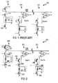
- FIG. 1 illustrates a block diagram of a conventional system 100.
- the conventional sensing system 100 comprises a reference column 130, a plurality of data columns, e.g., column 0 150 through column N 170, and a plurality of comparators 158, 178, etc.
- the reference column 130 comprises a reference memory cell 126, a MOS transistor 118 (cascoding transistor) and a diode connected MOS transistor 114 (pull-up or load transistor).
- a bitline RC component 122 is shown to indicate resistance and capacitance on the bitline.
- a ymux e.g., bitline selection circuit
- a ymux e.g., bitline selection circuit
- N:1 ymux i.e., comprised of an N quantity of MOS transistors which have all N drains connected together and N sources connects to N individual bitlines
- the ymux may be in series with transistor 118 and the bitline RC component 122, and the gates of the ymux MOS transistors may be decoded from a decoder (not shown).
- the ymux typically acts only as a dummy ymux (its gate is on all the times, typically connected to VDD) since there is typically only one reference cell 126, hence no selection is needed.
- the transistor118 may provide a cascoding function for the sensing, meaning its source is typically regulated at a bias voltage vblbias, e.g., 0.8-1.4V, by modulating its gate at vblbias+Vt of transistor 118, with Vt being its NMOS threshold voltage.
- the drain of the transistor 118 is the output node regarding the sensing, which varies According the magnitude of the cell current from the memory cell 126.
- the cascoding function of the transistor 118 serves to isolate the RC component 122 from the sensing node 154.
- the reference column 130 provides a voltage reference on the reference line, Vref, 154 which is applied to a first input of each of the comparators 158 through 178.
- Each data column 150 through 170 may comprises a data memory cell, a MOS transistor and a diode connected MOS transistor. Another bitline RC component represents resistance and capacitance on the bitline. The ymux of the data column 150-170 is not shown.
- Each of the data columns 150 through 170 provides a data output voltage V OUT0 through V OUTN to a second input of a respective comparator 158 through 178 so that the comparator provides an output indicative of the stored data in the corresponding data column.
- the conventional sensing system 100 has non-optimum operation, such as behavior stemming from the various MOS transistors (e.g., the diode connected MOS transistor 114 within the reference column 130). Error such as non-linear operation due to a load in the saturation region may then result, for example, in failure to provide the desired linear or near linear conversion of the transistor 114 cell saturation current (Icell-sat) into an output signal (Vout).
- FIG. 2 is a schematic diagram illustrating an exemplary system 200 implementing differential MOS transistors consistent with certain aspects related to the present innovations.
- sensing system 200 comprises a reference column 230, a plurality of data columns, e.g., column 0 250 through column N 270, and a plurality of comparators 258, 278, etc.
- the reference column 230 comprises a reference memory cell 226, a differential threshold MOS transistor 218 (e.g., cascoding transistor), and a diode-connected differential threshold MOS transistor 214 (e.g., pull-up, load transistor, etc.), which may be an NMOS or native NMOS transistor, with its gate and drain connected together and acting as an output voltage node (e.g., reference) for the reference column.
- An RC component 222 is shown to indicate resistance and capacitance on the reference column.
- a ymux associated with the reference column 230 is not shown.
- the reference column 230 provides a voltage reference on the reference line, Vref, 254 which is applied to a first input of each of the comparators 258 through 278.
- Each data column 250 through 270 may comprise data memory cells 274, 294, MOS (e.g., cascoding) transistors 266, 286, and diode connected differential threshold NMOS (e.g., pull-up, load, etc.) transistors 262, 282 with gate and drain terminals connected together, and acting as (e.g., data) output voltage nodes for their respective columns.
- a bitline RC component 272, 292 is also shown, representing resistance and capacitance on the bitline.
- the ymux of the data columns 250-270 i.e., coupling from the bitline components 272,292 and memory cells 274, 294 to the transistors 266, 286, respectively, are not shown.
- Each of the data columns 250 through 270 provides a data output voltage VOUT0 through VOUTN to a second input of a respective comparator 258 through 278 so that the comparator provides an output indicative of the stored data in the corresponding data column.
- Differential threshold MOS transistors 214, 262, 282 of exemplary system 200 may be transistors fabricated such that physical or electrophysical differences between the drain region/structure and the source region/structure produce a threshold voltage across the drain region, Vtnd, that differs from the threshold voltage across the source region, Vtns.
- Vtn refers to threshold voltage, Vt, of a NMOS transistor
- Vtnd refers to Vt of a NMOS across the drain region
- Vtns refers to Vt of a NMOS across the source region.
- exemplary operating conditions may yield a reference voltage of, e.g., 1.3 volts absent the present innovations.
- VDD 1.6V
- VT 0.1
- deltaVgs(Ids) 0.2
- the physics/structure of the MOS structures may be fabricated to alter threshold voltages/saturation characteristics of the differential threshold voltage MOS devices 214, 262, 282, involved in voltage determinations.
- Vtnd 0.1 volts
- MOS circuitry/devices that, in general, may benefit from such innovations include but are not limited to those with MOS transistors contributing to output voltage values/levels, those that trim offset, and those transitioning to or from on/off states based on small voltage swings at their nodes, among others.
- innovations enabling ability to set differing threshold voltages, such as Vtnd and/or Vtns, enable advantages like improved bitline operations, and further examples of which are detailed below.
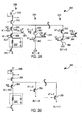
- FIG. 3A is a schematic diagram illustrating an exemplary system 300 implementing differential MOS transistors and/or otherwise consistent with certain aspects related to the present innovations.
- exemplary sensing system 300 may comprise a (pull-up or load) diode-connected transistor 314 (which may function similarly to the NMOS transistor 214 of Figure 2 ) with its gate and drain connected together and acting as a output voltage node, a cascoding differential threshold transistor 318, and a plurality of memory columns 330, 350, 370.
- the cascoding transistor 318 may benefit from differential threshold voltage construction as follows.
- Each memory column may comprise a ymux, an RC component, a memory cell, and a plurality of ymux transistors 320/324/328, 340/344/348, 360/364/368.
- Such ymux circuitry may be used, e.g., to select one bitline out of 8 bitlines to connect to the cascoding transistor 318 and load transistor 314.
- An RC element 322 is shown to represent resistance and capacitance on the first bitline and coupled to the ymux 321.
- a memory cell 326 may also be coupled to the RC component 322.
- a memory column refers to such combination of ymux, RC element and memory cell.
- additional RC elements as well as memory cells may be connected to the other seven bitlines BL[1:7]. The arrangement illustrated in FIG.
- differential threshold transistors 320, 324 may have on/off states reducing leakage, i.e., saturating or passing voltages from the selected bitline through to sensing circuitry to minimize loss.
- differential threshold transistors 320, 324 when, e.g., the first exemplary memory column 330 is selected, differential threshold transistors 320, 324 will be in linear operation and pass the voltage from the bitline (bitline 0) through to the sensing circuitry. Further, when exemplary bitline 0 is unselected, transistor 328 pulls up the node between transistors 320 and 324 to place a reverse bias on, and shut off, transistor 320.
- Each of the memory columns 330, 350 through 370 provides a data output signal to enable provision of an output indicative of the stored data in the corresponding memory column.
- FIG. 3B is a schematic diagram illustrating an exemplary system 380 implementing differential MOS transistors and/or otherwise consistent with certain aspects related to the present innovations.
- exemplary sensing system 380 may comprise a (e.g., pull-up, load, etc.) differential threshold PMOS transistor 389 with its gate and drain connected together and acting as a output voltage node, a cascoding differential threshold NMOS transistor 388 and a plurality of differential threshold NMOS transistors 382, 384, and 386 consistent with those set forth herein.
- the transistors 382, 384, 386 may, e.g., be part of a ymux 8:1 used to select a bitline out of eight bitlines to connect to the (pull-up, load) transistor 389.
- the transistors 382, 384, and 396 may be part of ymux circuits that belong to respective memory columns, with each memory column comprising a transistor of a ymux, a RC element and a memory cell.
- the first memory column comprises the NMOS transistor 382, RC element 322 and the shown memory cell.
- the other memory columns comprise transistor 384 and 386 (as part of ymux circuit), RC elements (not shown) and memory cells (not shown).
- an exemplary data column may comprise the transistor 389, the cascoding transistor 388 and a plurality of memory columns as set forth above.
- sensing systems consistent with that of FIG. 3B may utilize higher threshold voltage across the source, Vts, e.g., to enable innovative functionality, such as improved bitline/leakage control as with FIG. 3A , wider ranges of operating conditions or voltages, and/or other such threshold-based enhancements.
- exemplary transistors 388 (which may function similarly to the transistor 318 of Figure 3A ) and 389 (which may function similarly to transistor 314 of Figure 3A or 214 of Figure 2 ) may have a higher Vtd to enable an improved data out line voltage, e.g., improved to a wider operating voltage range, and transistors 382, 384, 386 may have a higher Vts to shut off the unselected bitlines with less leakage. Further, transistors 382, 384, 386 may have lowered drain threshold voltages to enhance their voltage passing function with less delay.
- FIG. 4 is a schematic diagram illustrating an exemplary system consistent with certain aspects related to the present innovations.
- another exemplary sensing system may include a differential sense amplifier 400 comprised of a reference column 410 and a plurality of output columns 440, 460. (Here again, as with FIGs.
- the reference column 410 may comprise a reference memory cell 432, a diode-connected differential threshold PMOS (e.g., pull-up, load, etc.) transistor 412 with its gate and drain connected together and acted as a output reference voltage node, and an additional reference column circuit 420, which may be characterized as having, e.g., at least one differential threshold NMOS (e.g., cascoding) transistor 422 and an RC component 430 representative of resistance and capacitance on the reference column 410 or circuit 420.
- the transistor 412 and 422 may function similarly to the transistor 314 and 318 of Figure 3A respectively.
- the reference column 410 sets a voltage reference 416 on the REFOUT line, which is supplied to an input of a differential input stage 440.
- Another input DATAOUT 452 of the differential input stage 440 is from a data column (not shown) similar to the reference column 210 with data memory cell.
- the output columns include a variety of amplifier circuits and/or stages to provide desired outputs, which may include a one or more differential threshold MOS (PMOS/NMOS) transistors, such as the exemplary transistors 442, 446, 444, 448, 450, 454, 456 shown in FIG. 4 .
- Each of the output columns may provide an output voltage, such as SAout, SAoutb (see, e.g.
- differential threshold voltage MOS transistors may improve the headroom (i.e., associated with transistor 422, etc.), for example by reducing the overall threshold voltage of such transistor.
- headroom i.e., associated with transistor 422, etc.
- performance can be improved by reducing the overall threshold voltage from 0.2, e.g., to approximately 0.1 to 0.
- improvement may be effected via utilization of the innovations herein, e.g., using a differential voltage NMOS transistor 422 having a higher drain threshold voltage 424 fixed to offset the source threshold voltage 426 and provide an overall effective threshold voltage of approximately 0.1 to 0.
- transistor 422 may act as a cascoding transistor similar to transistor 218 of Figure 2 , hence may benefit from differential threshold construction similar to that of the transistor 318 of Figure 3A .
- transistor 412 e.g., pull-up, load, etc. transistor
- the input pair 444 and 448 can be used similar to that of the transistor 422.
- Transistors 442, 446, 454 may also be implemented in a similar manner to that of transistor 412.
- transistors 450, 456 can be implemented similarly to that of transistor 422.
- FIG. 5 is a schematic diagram illustrating exemplary systems consistent with certain aspects related to the present innovations.
- two exemplary threshold voltage indicating arrangements 520, 560 are illustrated.
- a first arrangement 520 illustrates an exemplary arrangement enabling measurement of a source threshold voltage Vtns 530.
- first arrangement 520 may include a supply 524, an input signal controlling element, a differential, threshold MOS transistor 522 that is diode connected across its drain 528, and a sink 526 to ground Via control of the input signal controlling element and placing the drain and gate at the same voltage, an accurate measurement of the source threshold voltage Vtns may be taken via measurement of the overall threshold voltage for the transistor 522 Similarly, FIG.
- the second arrangement 560 may include a supply 564, an input signal controlling element, a differential threshold MOS transistor 562 that is diode connected across its source 568, and a sink 566 to ground.
- a drain threshold voltage Vtnd 570 may be taken via measurement of the overall threshold voltage for the transistor 562.
- FIG. 6 is a schematic diagram illustrating an exemplary system consistent with certain aspects related to the innovations herein.
- FIG. 6 illustrates a differential pass gate circuit 600 including a differential threshold MOS transistor 612 with, e.g., a drain region 608 having a higher drain threshold voltage, Vtnd, than the threshold voltage, Vtns, of the source 610.
- Vtnd drain threshold voltage
- Vtns threshold voltage
- Such arrangements provide advantages, for example, when passing a high voltage (the high voltage will effectively cause a high Vt to be lowered via drain induced barrier lowering) as well as more effective shut off due to the presence of a high Vt region.
- FIG. 7 is a schematic diagram illustrating an exemplary system consistent with certain aspects related to the present innovations.
- a power on reset system 700 is illustrated including a plurality of differential threshold MOS transistors 704, 734, 744 and an output node 746 Vtrip.
- Conventional power on reset systems often suffer the drawback that the power on output, Vtrip, level is too high at low VDD in that it must be greater than or equal to, for example the sum of threshold voltages of transistors completing the circuit (i.e., transistors corresponding to transistor 704, which would be diode connected in a conventional circuit, and transistor 744).
- differential threshold voltage MOS transistors 704, 734, 744 may be utilized to manipulate the output Vtrip within improved operating margins.
- a first differential transistor 704 in linear region when operating; and not diode connected
- a pair of output transistors 734, 744 may also each include a source threshold voltages 738, 748 set higher than one or both of their drain threshold voltages or than comparable (standard logic) transistors in corresponding conventional power on systems.
- Such arrangements enable lower "on" values to be achieved at the upper range of the output Vtrip in that the output high point (Vtriph 766 in FIG.
- the power on reset may simply be tripped at the highest threshold voltage associated with such transistors, rather than the sum of threshold voltages.
- such systems 700 may be ANDed with a NAND gate for enabling or disabling POR, i.e., for testing, to prevent glitches, to allow reading at values less than the POR trip point (such as by a register bit or command), etc.
- FIG. 7B is a graph illustrating performance characteristics consistent with the exemplary system of FIG. 7 , according to certain aspects related to the present innovations.
- a power on reset (“POR") level 768 is shown graphed against a range of VDD voltage 762 to illustrate exemplary fluctuations in the output high point for POR Vtriph 766.
- POR power on reset
- Vtriph as the sum of the two threshold voltages, would be too high for the circuit to operate properly at low VDD (i.e., as VDD approached Vtriph 766.
- the present innovation enable Vtriph to effect its reset operation when either transistor is on.
- Vtriph may be tripped at the higher of the two threshold voltages, enabling, for example, improved operating margins at low VDD.
- This functionality may be achieved via differential threshold MOS transistor
- physical dimensions may be configured to achieve higher trip point voltage due to higher threshold voltages resulting from dimensional changes or effects (such as due to short channel effect, short width effect, reverse width effect, litho-related effect, well proximity effect, OD (source/drain diffusion dimension), etc). This may be achieved, for example, via sampling different dimensions (width and length) around a peak value such as threshold voltage versus width, channel length, or OD (source/drain diffusion dimension) for the relevant transistor, such as transistors 704 and 744, here.
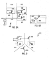
- FIGs. 8A and 8B are diagrams illustrating a schematic and graph of another exemplary circuit/system consistent with FIGs. 7A and 7B , though reflecting differing aspects (sources and/or drains) with varied threshold voltages at different locations in such circuits.
- FIG. 9 is a schematic diagram illustrating an exemplary system consistent with certain aspects related to the present innovations.
- a system 900 is disclosed including a differential pair of MOS devices 920, 940. Improved operation may be achieved when the output device 940 is implemented using one or more low threshold voltage transistors consistent with the innovations herein.
- low threshold voltage device 940 may be implemented via a plurality of MOS transistors with at least two or more of the transistors having different lengths.
- output device 940 may be implemented with 3 MOS transistor subcomponents at shown in FIG. 16 , each with differing lengths, e.g., 5/0.3, 5/0.35, 5/0.4, etc.
- output device may also be implemented with composite devices, as set forth below, to realize the lower threshold voltage parameter desired for the output device 940.
- Such exemplary implementations also having overall advantages consistent with averaging threshold voltages across the source to minimize offset of the differential pair.
- FIGs. 10A and 10B are schematic diagrams illustrating exemplary systems consistent with certain aspects related to the present innovations.
- an exemplary system 1010 is disclosed including a plurality of transistors 1012, 1014, 9018 and a ratio-based latching device comprised of a first circuit 1022 and a second circuit 1034.
- System 1010 illustrates one exemplary use of differential threshold MOS devices or transistors to improve feedback-related operating margins.
- System 1010 shows differential threshold MOS transistors 1024, 1036 including source threshold voltages 1026, 1038 being different (in this example, higher) than their corresponding drain threshold voltages (and, hence, being higher than threshold voltage(s) of standard transistors) to provide better control of the relevant feedback and latching operations.
- exemplary system 1010 enables improved voltage operating margins (here, improved voltage ratios or ranges) for feedback operations via use of differential threshold voltages to control, for example, latching of earlier circuitry as a function of circuit output.
- Second exemplary circuit 1050 shows another representative illustration of first and second circuits 1052, 1062 that use of differential threshold voltages to control leakage.
- differential threshold MOS transistors 1054, 1064 include source threshold voltages 1060, 1066 set to be different (in this example, higher) than their corresponding drain threshold voltages (yielding higher threshold voltage(s) than standard transistors) to provide better control of the on/off states to, inter alia, reduce leakage.
- differential MOS transistors 1054, 1064 will saturate or pass voltages with less transition and delay than a higher standard threshold voltage transistor, thereby minimizing loss.
- higher source (and lower drain) threshold voltages 1060, 1066 in the two MOS transistors 1054, 1064 will provide switching within narrower margins, more succinct transitioning ranges, and/or less leakage.
- FIG. 11A is a cross-sectional view of an exemplary MOS transistor device consistent with certain aspects related to the innovations herein.
- the underlying fabrication processes of such devices are well known to those skilled in the art; examples of these processes include U.S. Patent Nos. 5,045,488 , and 6,258,645 , and 6,329,685 , which are incorporated herein by reference in entirety.
- a MOS transistor 1100 may comprise a substrate 1110 of semiconductor material of a first conductivity type, such as a P-substrate, the substrate including source and drain regions 1144, 1142.
- source and drain regions 1144, 1142 may include regions of a second conductivity type, such as upper N+ doped regions 1144a, 1144b provided, e.g., via an Arsenic (As) implantation process, lower N+ doped regions 1142a, 1142b provided, e.g., via a Phosphorus (P) implantation process.
- the source and drain regions 1144, 1142 are spaced apart from each other defining a channel region 1140 therebetween.
- An insulating layer 1120 is disposed over the channel region of the substrate, including a first insulating portion 1120a proximal to the first source/drain region and a second insulating portion 1120b proximal to opposed source/drain region.
- a gate portion 1130 is disposed above the insulating layer. Further, the channel region 1140 comprises opposed junction regions including a first junction region 1160a adjacent one source/drain region 1144a, 1142a and a second junction region 1160b adjacent the complementary source/drain region 1144b, 1142b.
- the MOS transistor may also include an inversion region 1146.
- one or both of the shape or the implantation i.e., type or composition of implantation, density of implantation, concentration of implantation, and/or variation through a transition region, etc.
- the shape or the implantation i.e., type or composition of implantation, density of implantation, concentration of implantation, and/or variation through a transition region, etc.
- the shape or the implantation are of varying dimension to provide a first threshold voltage associated with that junction region which differs from a second threshold voltage associated with the opposed junction region.
- the semiconductor materials comprising the region may be of a different shape or size than that of the opposed region to impart this differing threshold voltage
- the implantation may be of differing type or composition (doped with differing ions/compounds, dosages, processes and angles, etc.), of differing density/concentration, of varying size, location, strength, or of variations of two or more of such differences, and/or the threshold voltage may be set differently based on combinations of the above.
- an area of higher depletion may be formed at the first junction region 1150a via creation of a larger supplemental implant 1148a, such as P+ implant of, e.g., Boron (B), other Halo materials, etc.
- a larger supplemental implant 1148a such as P+ implant of, e.g., Boron (B), other Halo materials, etc.
- P+ implant e.g., Boron (B)
- B Boron
- supplemental implants consistent with aspects of the present innovations provide for particularized barrier loading features applicable to the circuitry disclosed herein.
- the threshold voltage of the first junction region e.g., drain
- the threshold voltage of the first junction region may be set higher (e.g., 50mV-500mV, etc.) than that of opposed junction region, via such drain-induced barrier loading, based on the variations set forth above, such as dose and angle.
- one or both of shape and implantation of the first junction region or the second junction region may be varied via a supplemental implant to provide a device having different threshold voltages as a function of the supplemental implant.
- shape and/or the implantation of the first junction region or the second junction region may be varied via one or more supplemental implants to provide a device having different threshold voltages as a function of the one or more supplemental implants.
- FIG. 11B a graph illustrating exemplary performance features of a exemplary device consistent with certain aspects related to the present innovations.
- Graph 1150 is a graph of drain to source current, Ids, 1122 versus drain to source voltage, Vds, 1110 illustrating characteristics of a junction having such an exemplary supplemental implant.
- Rout will increase inversely as the slope of 1/ A decreases, as shown by the series of slopes 1114, 1116, 1118, which illustrate increasing gain (Rout) with increased doping.
- FIG. 12 is a perspective (side) view of an exemplary device consistent with certain aspects related to the present innovations.
- the MOS device 1200 of FIG. 12 includes some of the same or similar features as that of FIG. 12 , though illustrating some features associated with the oxide or insulating layer to provide a differing threshold voltage for one source/drain as opposed to the other.
- a MOS transistor 1200 may comprise a substrate 1210 of semiconductor material of a first conductivity type, such as a P- substrate, the substrate including source and drain regions 1244, 1242.
- source and drain regions 1244, 1242 may include regions of a second conductivity type, such as upper N+ doped regions 1244a, 1244b provided, e.g., via an Arsenic (As) implantation process, lower N+ doped regions 1242a, 1242b provided, e.g., via a Phosphorus (P) implantation process.
- the source and drain regions 1244, 1242 are spaced apart from each other defining a channel region 1240 therebetween.
- An oxide/insulating region 1220 is disposed over the channel region of the substrate. Additionally, a gate portion 1230 is disposed above the oxide/insulating region 1220.
- the channel region 1240 comprises opposed junction regions including a first junction region 1260a adjacent one source/drain region 1244a, 1242a and a second junction region 1260b adjacent the complementary source/drain region 1244b, 1242b.
- the MOS transistor may also include an inversion region 1246.
- an exemplary oxide/insulating region 1220 may include one or more oxide or other insulating/dielectric layers 1222, and a nitride layer 1224 that utilizes nitride charge trapping with loci (see, e.g., trapped charge 1226 shown in FIG. 12 for purposes of illustration) at the source and drain regions to control source threshold voltage, Vts, and drain threshold voltage, Vtd.
- loci see, e.g., trapped charge 1226 shown in FIG. 12 for purposes of illustration
- Vts source threshold voltage
- Vtd drain threshold voltage
- the trapped charge 1226 is depicted in FIG. 12 for purposes of illustration, the charge trapping region or regions may also be characterized as being adjacent the source or drain to control the corresponding threshold voltage. Further, with the present example is described in the context of nitride, charge trapping regions of other composition may otherwise be utilized. Similarly, while the present exemplary charge trapping region is described in the context of a layer, other shapes and arrangements of materials may also be used.
- loci or regions of trapped charge at the source, or manipulations of the source threshold voltage can be used in exemplary systems set forth herein, including but not limited to trimming the offset of differential pairs in comparators or operational amplifiers.
- Such loci or regions of trapped charge at the drain, or manipulations of the drain threshold voltage can also be used in exemplary systems set forth herein, including but not limited to trimming the operating point at drain side, for example, of a differential pair in comparators or operational amplifiers.
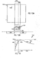
- FIGs. 13A and 13B are perspective (top and side) views of an exemplary device consistent with certain aspects related to the present innovations.
- Exemplary MOS semiconductor device 1300 shown in FiGs. 13A and 13B may include a substrate of semiconductor material of a first conductivity type 1310, source/drain regions 1344 in the substrate, wherein the source region and the drain region are of a second conductivity type and spaced apart from each other defining a channel region therebetween, an insulating layer 1322 disposed over the channel region of the substrate, and a gate portion over the insulating layer.
- the insulating layer 1322 may be viewed as being composed of opposed insulating regions or "portions," including a first insulating portion 1322 adjacent the first source/drain region and a second insulating portion 1326 adjacent the opposed source/drain region, wherein each insulating portion defines or characterizes a threshold voltage between the gate and the source/drain associated with each insulating portion.
- the first insulating portion or the second insulating portion may fabricated with varying dimension, including thickness 1334, to provide a first threshold voltage that differs from a second threshold voltage associated with the opposed insulating portion.
- Dimensions that may be varied in the insulating layer to achieve these advantages include the thickness 1334 as well as the widths (distance or dimension across channel) 1333, 1331 of the first insulating portion 1324 and the second insulating portion 1326.
- this second insulating portion represents an oxide region of less thickness than the first insulating portion
- the linear dimension of the width 1331 may be decreased to reduce the threshold voltage, similar in function to dimensional changes to depletion regions that may impart change to voltage characteristics.
- a threshold voltage decrease may also be effected via reduction(s) in width to the first and/or second insulating portions. Further, use of thicker oxide for the second insulating portion 1326 will make for a higher threshold voltage across the associated (adjacent) source/drain.
- Oxide dimensioning may also be characterized as taking the form of an offset region or offset 1336 in the overall insulating layer 1322.
- the offset may be a region defined by, such as a substantially rectilinear shape over the source/drain region for which a differential threshold voltage is desired.
- dimensioning consistent with the above may impart differential threshold voltage conditions between source and drain on the order of about 0.1 volts to about 0.5 volts.
- FIG. 14 is a graph illustrating performance features/characteristics of an exemplary device consistent with certain aspects related to the present innovations.
- Graph 1400 of FIG. 14 is an exemplary graph of threshold voltage 1462 versus length 1464 for exemplary devices such as the MOS transistor shown in FIG. 13 .
- Graph 1400 helps illustrate a representative relationship between the threshold voltage associated with, for example, second insulating portion 1326 as its length 1331 dimension varies. As shown, when the length dimension is in its smaller range (characterized, inter alia, via line Lmin 1471) the graph of voltage versus length is characterized by a curve of positive slope, or a threshold voltage that increases as length increases (also referred to as SCE or Short Channel Effect).
- a maximum threshold voltage may be established and shifted according to design and fabrication parameters, and a minimum threshold voltage may be determined or established as a function of short length characteristics.
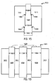
- FIG. 15 is a perspective (top) view of an exemplary device consistent with certain aspects related to the present innovations.
- a composite device 1500 is shown including a substrate 1510 with source/drain regions, and an oxide region 1530 of varying dimension.
- a metal oxide semiconductor device may include a substrate 1510 of semiconductor material of a first conductivity type, a source region and a drain region in the substrate, wherein the source region and the drain region are of a second conductivity type and spaced apart from each other defining a channel region therebetween, an insulating layer 1530 disposed over the channel region of the substrate, and a gate portion above the insulating layer.
- the oxide region 1530 may be characterized as having first and second parts or "insulating portions," similar to those set forth above; each associated with complementary source and drain regions.
- the first insulating portion or the second insulating portion is fabricated of varying length and width, and of different dimension than the opposed insulating portion, to provide a first threshold voltage that differs from a second threshold voltage associated with the opposed insulating portion.
- exemplary oxide region 1530 is shown with 3 portions 1550, 1554, 1558 of differing width (i.e., distance across channel).
- Each of these portions may also be characterized by transition regions 1552, 1556 that reflect changes from each region's differing length and width.
- transition regions 1552, 1556 that reflect changes from each region's differing length and width.
- each of the 3 overall regions would then typically be characterized by differing threshold voltages, with an overall or composite threshold voltage for each source or each drain being determined as a function of each threshold voltage subcomponent.
- FIG. 16 is a perspective (top) view of an exemplary device consistent with certain aspects related to the present innovations.
- a series device 1600 is shown including a substrate 1610 with source/drain regions, and oxide regions 1630 of varying length.
- a metal oxide semiconductor device may include two or more transistor subcomponent electrically arranged in series, each transistor subcomponent including a substrate 1610 of semiconductor material of a first conductivity type, a source region and a drain region in the substrate, wherein the source regions and the drain regions are of a second conductivity type and spaced apart from each other defining channel regions therebetween, one or more insulating layers 1630 disposed over the channel region of the substrate, each having a gate portion located above the insulating layer.
- the illustration of FIG. 16 depicts 3 transistor subcomponents, although embodiments with two or with more than 3 may also be consistent with the innovations herein.
- exemplary MOS device 1600 includes a first oxide region 1632 ("first insulating portion") of a first transistor subcomponent, a second oxide region 1634 ("second insulating portion") of a second transistor subcomponent, and a third oxide region 1636 (third insulating portion") of a third transistor subcomponent.
- Structures having two transistor elements may, for example, be characterized as having a first insulating portion of a first transistor fabricated of a first length (i.e., distance across the first channel) that is different than a second length of a second insulating portion of a second transistor subcomponent.
- Oxide regions placed in such series relationship to each other, define various threshold voltages for each subcomponent with the highest threshold voltage determining the overall or composite threshold voltage of the device, and may thereby provide a first threshold voltage of the device that differs from a second threshold voltage of the device.
- structures have three or more transistor elements may include similar relationships between all of the various transistor oxide regions.
- FIG. 17 is a perspective (top) view of an exemplary device consistent with certain aspects related to the present innovations.
- a composite device 1700 is shown including a substrate 1710 width source/drain regions, and an oxide region 1768 of varying dimension.
- a metal oxide semiconductor device may include a substrate 1710 of semiconductor material of a first conductivity type, a source region and a drain region in the substrate, wherein the source region and the drain region are of a second conductivity type and spaced apart from each other defining a channel region therebetween, an insulating layer 1768 disposed over the channel region of the substrate, and a gate portion above the insulating layer.
- the oxide region 1768 may be characterized as having first and second parts or "insulating portions," similar to those set forth above, each associated with complementary source and drain regions. As shown by way of example in the illustration of FIG. 17 , the first insulating portion or the second insulating portion is fabricated of varying length and/or of different surface area or volumetric dimension in the length direction than the opposed insulating portion, to provide a first threshold voltage that differs from a second threshold voltage associated with the opposed insulating portion. In FIG.
- exemplary oxide region 1768 may be varied on one side or insulating portion 1770, adjacent to a source or drain region, by lengthening or shortening the two length dimensions L1, L2 of the oxide layer adjacent that source/drain.
- the two differing insulating portions, one on each side of the channel, would then typically be characterized by differing threshold voltages.
Landscapes
- Engineering & Computer Science (AREA)
- Computer Hardware Design (AREA)
- Metal-Oxide And Bipolar Metal-Oxide Semiconductor Integrated Circuits (AREA)
- Semiconductor Memories (AREA)
- Read Only Memory (AREA)
- Non-Volatile Memory (AREA)
Claims (20)
- Erfassungsschaltung (200), umfassend:eine Referenzspalte (230), die einen Referenzspannungsknoten, eine Referenzspeicherzelle (226), einen ersten MOS-Transistor (218) und einen ersten differenziellen Schwellenspannung-MOS-Transistor (214) enthält; undeine Mehrzahl von Datenspalten (250, 270), die jeweils gekoppelt sind an einen entsprechenden Datenspannungsknoten parallel zu der Referenzspalte (230), wobei jede Datenspalte eine Datenspeicherzelle (274, 294), einen zweiten MOS-Transistor (266, 286) und einen zweiten differenziellen Schwellenspannung-MOS-Transistor (262, 282) umfasst;wobei einer oder mehr der differenziellen Schwellenspannung-Transistoren (214; 262, 282) Transistoren sind, die jeweils eine Gate-Source-Schwellenspannung aufweisen, die sich von einer Gate-Drain-Schwellenspannung unterscheidet.
- Erfassungsschaltung (200) nach Anspruch 1, wobei einer oder mehr der differenziellen Schwellenspannung-Transistoren (214; 262, 282; 1100) umfassen:ein Substrat (1110) von Halbleitermaterial einer ersten Leitfähigkeitsart;einen ersten Bereich (1144) und einen zweiten Bereich (1142) in dem Substrat (1110), wobei der erste und der zweite Bereich (1144, 1142) von einer zweiten Leitfähigkeitsart sind und voneinander derart beabstandet sind, dass ein Kanalbereich (1140) dazwischen definiert wird;eine Isolierschicht (1120), welche über dem Kanalbereich (1140) des Substrats (1110) angeordnet ist, wobei die Isolierschicht (1120) entgegengesetzte Isolierbereiche umfasst, welche einen ersten Isolierbereich (1120a) benachbart zum ersten Bereich (1144) und einen zweiten Isolierbereich (1120b) benachbart zum zweiten Bereich (1142) enthalten; undeinen Gate-Bereich (1130) oberhalb der Isolierschicht (1120);wobei jeder Isolierbereich (1120a, 1120b) eine Schwellenspannung zwischen dem Gate (1130) und dem ersten Bereich (1144) oder dem zweiten Bereich (1142) benachbart zu jedem Isolierbereich (1120a, 1120b) charakterisiert; undwobei der erste Isolierbereich (1120a) mit variierender Dimension hergestellt ist, welche eine erste Dicke enthält, die sich von einer zweiten Dicke des zweiten Isolierbereichs (1120b) derart unterscheidet, dass eine erste Schwellenspannung bereitgestellt wird, welche sich von einer zweiten Schwellenspannung unterscheidet, die dem entgegengesetzten Isolierbereich zugeordnet ist.
- Erfassungsschaltung (200) nach Anspruch 1 oder 2, wobei der erste MOS-Transistor (218) ein kaskodierender Transistor ist; und/oder
wobei ein oder mehr der ersten und/oder der zweiten differenziellen Schwellenspannung-MOS-Transistoren (214; 262, 282) Dioden verbunden und/oder NMOS- oder native NMOS-Transistoren sind; und/oder
wobei ein oder mehr der Datenspannungsknoten jeweils mit einem Vergleicher (258, 278) gekoppelt sind; oder
wobei jeder Datenspannungsknoten mit einem Vergleicher (258, 278) gekoppelt ist. - Erfassungsschaltung (200) nach Anspruch 1 oder 2, wobei ein oder mehr der differenziellen Schwellenspannung-Transistoren (214; 262, 282) kaskodierende Transistoren sind; und/oder
wobei ein oder mehr der differenziellen Schwellenspannung-MOS-Transistoren (214; 262, 282; 1100) Transistoren sind, welche einen Kanalbereich (1140) aufweise, der einen ersten Sperrschichtbereich (1160a) und einen zweiten Sperrschichtbereich (1160b) enthält, wobei eine Form des ersten Isolierbereichs (1120a) oder eine Form oder Implantation des ersten Sperrschichtbereichs (1160a) von variierender Dimension derart ist, dass eine Gate-Source-Schwellenspannung bereitgestellt wird, die sich von einer Gate-Drain-Schwellenspannung unterscheidet, die über eine Dimension des zweiten Isolierbereichs (1120b) und/oder des zweiten Sperrschichtbereichs (1160b) bestimmt wird. - Schaltung (200) nach Anspruch 2, wobei ein oder mehr der differenziellen Schwellenspannung-Transistoren (214; 262, 282; 1100) einen Kanalbereich (1140) umfassen, welcher einen ersten Sperrschichtbereich (1160a) benachbart zu einem ersten Bereich (1144a, 1142a) und einen zweiten Sperrschichtbereich (1160b) benachbart zu einem zweiten Bereich (1144b, 1142b) enthält; und
wobei eine Form des ersten Isolierbereichs (1120a) oder eine Form oder Implantation des ersten Sperrschichtbereichs (1160a) von einer variierenden Dimension derart ist, dass eine Gate-Source-Schwellenspannung bereitgestellt wird, die sich von einer Gate-Drain-Schwellenspannung unterscheidet, die über eine Dimension des zweiten Isolierbereichs (1120b) und/oder des zweiten Sperrschichtbereichs (1160b) bestimmt wird; und/oder
wobei ein oder mehr der differenziellen Schwellenspannung-Transistoren (214; 262, 282; 1100) einen Kanalbereich (1140) enthalten, welcher Sperrschichtbereiche (1160a, 1160b) umfasst, die einen ersten Sperrschichtbereich (1160a) benachbart zum ersten Bereich (1144a, 1142a) und einen zweiten Sperrschichtbereich (1160b) benachbart zum zweiten Bereich (1144b, 1142b) enthalten; wobei der erste Sperrschichtbereich (1160a) und der zweite Sperrschichtbereich (1160b) entgegengesetzt voneinander sind;
wobei eine Form oder Implantation des ersten Sperrschichtbereichs (1160a) und/oder des zweiten Sperrschichtbereichs (1160b) von variierender Dimension derart ist, dass eine erste Schwellenspannung bereitgestellt wird, die sich von einer zweiten Schwellenspannung unterscheidet, die dem entgegengesetzten Sperrschichtbereich zugeordnet ist; und/oder
wobei vorzugsweise eine Form und Implantation des ersten Sperrschichtbereichs (1160a) und/oder des zweiten Sperrschichtbereichs (1160b) über zusätzliche Implantation derart variiert sind, dass ein Gerät bereitgestellt wird, welches unterschiedliche Schwellenspannungen als eine Funktion des Aussparungsimplantats ausweist; und/oder
wobei vorzugsweise Implantation des ersten Sperrschichtbereichs (1160a) oder des zweiten Sperrschichtbereichs (1160b) über zusätzliche Implantation derart variiert ist, dass ein Gerät bereitgestellt wird, welches unterschiedliche Schwellenspannungen als eine Funktion des Aussparungsimplantats aufweist; und/oder
wobei vorzugsweise die variierte Dimension der Implantation ein oder mehr von Variationen im Typ oder Zusammensetzung von Implantation, Dichte von Implantation, Konzentration von Implantation und/oder Variation über einen Übergangsbereich des ersten Sperrschichtbereichs (1160a) enthält; und/oder
wobei vorzugsweise die Implantation von unterschiedlicher Zusammensetzung sein kann, die enthält, dass sie mit unterschiedlichen Ionen/Verbindungen dotiert ist, unterschiedliche Dosierungen aufweist, durch unterschiedliche Prozesse gebildet ist und/oder mit unterschiedlichen Winkeln hergestellt ist; und/oder
wobei vorzugsweise die Implantation durch ein oder mehr von unterschiedlicher Dichte/Konzentration, variierender Größe, Lage oder Stärke und/oder Variationen von zwei oder mehr solcher Unterschiede gekennzeichnet ist; und/oder
wobei vorzugsweise die Form und die Implantation des ersten Sperrschichtbereichs (1160a) oder des zweiten Sperrschichtbereichs (1160b) über ein oder mehr zusätzliche Implantate derart variiert sind, dass ein Gerät bereitgestellt wird, welches unterschiedliche Schwellenspannungen als eine Funktion der ein oder mehr zusätzlichen Implantate aufweist; und/oder
wobei ferner vorzugsweise ein Ladungsfallenbereich benachbart zur Source oder Drain dazu umfasst ist, dass die erste Schwellenspannung oder die zweite Schwellenspannung gesteuert wird. - Schaltung (200) nach Anspruch 1 oder 2, wobei ein oder mehr der differenziellen Schwellenspannung-Transistoren (214; 262, 282; 1200) umfassen:ein Substrat (1210) von Halbleitermaterial einer ersten Leitfähigkeitsart;einen ersten Bereich (1244) und einen zweiten Bereich (1242) in dem Substrat (1210), wobei der erste Bereich (1244) und der zweite Bereich (1242) von einer zweiten Leitfähigkeitsart sind und derart voneinander beabstandet sind, dass ein Kanalbereich (1240) dazwischen definiert wird;einen Ladungsfallenbereich, welcher eine erste Schwellenspannung liefert, die dem ersten Bereich (1244) zugeordnet ist, oder eine zweite Schwellenspannung liefert, die dem zweiten Bereich (1242) zugeordnet ist; undwobei vorzugsweise der Ladungsfallenbereich Nitrid ist; und/oder wobei vorzugsweise der Ladungsfallenbereich eine Schicht ist.
- Erfassungsschaltung (200) nach Anspruch 2, wobei die erste Dicke über Entfernen eines Offsetbereichs (1336) von der Isolierschicht (1322) variiert wird; und/oder
wobei vorzugsweise eine Breite des ersten Isolierbereichs (1324) derart variiert wird, dass für unterschiedliche erste Schwellenspannung gesorgt wird; und/oder
wobei vorzugsweise eine Breite des ersten Isolierbereichs (1324) derart variiert wird, dass für unterschiedliche erste Schwellenspannung gesorgt wird; und/oder
wobei vorzugsweise der erste Isolierbereich (1324) einen Bereich von Oxidmaterial dazu enthält, welches von der Isolierschicht (1322) entfernt wurde, dass eine Schwellenspannung herbeigeführt wird, die sich von der zweiten Schwellenspannung des zweiten Isolierbereichs (1326) unterscheidet. - Schaltung (200) nach Anspruch 7, wobei der Bereich von Oxidmaterial, welcher entfernt wurde, in der Form eines Offsetbereichs (1336) ist; und/oder wobei der Offsetbereich (1336) im Wesentlichen geradlinig geformt ist.
- Schaltung (200) nach Anspruch 2, wobei die variierende Dimension eine Änderung in einer Schwellenspannung von ungefähr 01, Volt bis ungefähr 0,5 Volt herbeiführt.
- Schaltung (200) nach Anspruch 2, ferner umfassend einen Ladungsfallenbereich benachbart zum ersten Bereich (1144) oder zum zweiten Bereich (1142), um die erste Schwellenspannung und/oder die zweite Schwellenspannung zu steuern.
- Erfassungsschaltung (200) von Anspruch 1, wobei ein oder mehr der differenziellen Schwellenspannung-Transistoren (214; 262, 282; 1300) umfassen:ein Substrat (1310) von Halbleitermaterial einer ersten Leitfähigkeitsart;einen ersten Bereich (1344) und einen zweiten Bereich (1344) in dem Substrat (1310), wobei der erste Bereich (1344) und der zweite Bereich (1344) von einer zweiten Leitfähigkeitsart sind und derart voneinander beabstandet sind, dass ein Kanalbereich dazwischen definiert wird;eine Isolierschicht (1322), die über dem Kanalbereich des Substrats (1310) angeordnet ist, wobei die Isolierschicht (1322) entgegengesetzte Isolierschichten umfasst, die eine erste Isolierschicht (1324) benachbart zum ersten Bereich (1344) und einen zweiten Isolierbereich (1326) benachbart zum zweiten Bereich (1344) enthalten, und wobei jeder Isolierbereich (1324, 1326) eine Schwellenspannung zwischen dem Gate und dem ersten Bereich (1344) oder dem zweiten Bereich (1344) definiert, die jedem Isolierbereich (1324, 1326) zugeordnet ist; undeinen Gate-Bereich oberhalb der Isolierschicht (1322);wobei der erste Isolierbereich (1324) oder der zweite Isolierbereich (1326) mit variierender Länge und Breite und mit einer Dimension, die sich vom entgegengesetzten Isolierbereich unterscheidet, derart hergestellt ist, dass eine erste Schwellenspannung bereitgestellt wird, die sich von einer zweiten Schwellenspannung unterscheidet, die dem entgegengesetzten Isolierbereich zugeordnet ist.
- Erfassungsschaltung (200) nach Anspruch 11, wobei vorzugsweise der erste Isolierbereich (1324) oder der zweite Isolierbereich (1326), welcher mit variierender Länge hergestellt ist, ebenfalls mit variierender Breite hergestellt ist; und/oder
wobei vorzugsweise die Isolierschicht (1322) Übergänge von einem niedriger zu einem höheren Oberflächenbereich derart sind, dass die erste Schwellenspannung bereitgestellt wird, welche sich von einer entgegengesetzten Schwellenspannung unterscheidet; und/oder
wobei vorzugsweise die Isolierschicht (1322) aus einer Mehrzahl von Bereichen von zwei oder mehr unterschiedlichen Längen und/oder Breiten gebildet ist, wobei Abgrenzung zwischen der Mehrzahl von Bereichen durch Übergangsbereiche gekennzeichnet ist, welche einen Übergang von Bereichen unterschiedlicher Länge und/oder Breite widerspiegeln, wobei jeder der Mehrzahl von Bereichen durch unterschiedliche Schwellenspannungen charakterisiert ist; und/oder
wobei vorzugsweise eine gesamte oder zusammengesetzte Schwellenspannung für jede Source oder jedes Drain als eine Funktion von jeder Schwellenspannungsunterkomponente bestimmt ist; und/oder
ferner vorzugsweise umfassend einen Ladungsfallenbereich benachbart zur Source oder Drain dazu, dass die erste Schwellenspannung und/oder die zweite Schwellenspannung gesteuert wird. - Erfassungsschaltung (200) nach Anspruch 1, wobei ein oder mehr der differenziellen Schwellenspannung-Transistoren (214; 262, 282; 1300) ein Metalloxid-Halbleitergerät enthalten, welches umfasst:ein Substrat (1310) von Halbleitermaterial einer ersten Leitfähigkeitsart;einen ersten Bereich (1344) und einen entgegengesetzten zweiten Bereiche (1344) in dem Substrat (1310), wobei der erste Bereich (1344) und der zweite Bereich (1344) von einer zweiten Leitfähigkeitsart sind und derart voneinander beabstandet sind, dass ein Kanalbereich dazwischen definiert wird;eine Isolierschicht (1322), die über dem Kanalbereich des Substrats (1310) angeordnet ist, wobei die Isolierschicht (1322) entgegengesetzte Isolierbereiche umfasst, die einen ersten Isolierbereich (1324) benachbart zum ersten Bereich (1344) und einen zweiten Isolierbereich (1326) benachbart zum zweiten Bereich (1344) enthalten, und wobei jeder Isolierbereich (1324, 1326) eine Schwellenspannung zwischen dem Gate und dem ersten Bereich (1344) oder dem zweiten Bereich (1344) definiert, die jedem Isolierbereich (1324, 1326) zugeordnet ist; undeinen Gatebereich oberhalb der Isolierschicht (1322);wobei der erste Isolierbereich (1324) oder der zweite Isolierbereich (1326) mit einer Dimension, die eine variierende Länge enthält, hergestellt ist, die sich vom entgegengesetzten Isolierbereich unterscheidet, derart, dass eine erste Schwellenspannung bereitgestellt wird, die sich von einer zweiten Schwellenspannung unterscheidet, die dem entgegengesetzten Isolierbereich zugeordnet ist.
- Erfassungsschaltung (200) nach Anspruch 13, wobei vorzugsweise die unterschiedliche Dimension ferner unterschiedliche Oberflächenbereiche oder Volumendimension in der Längenrichtung enthält; und/oder
ferner vorzugsweise umfassend einen Ladungsfallenbereich benachbart zur Source oder Drain dazu, dass die erste Schwellenspannung und/oder die zweite Schwellenspannung gesteuert wird. - Erfassungsschaltung (200) nach Anspruch 1, wobei ein oder mehr der differenziellen Schwellenspannung-Transistoren (214; 262, 282; 1600) ein Metalloxid-Halbleitergerät enthält, umfassend:zwei oder mehr MOS-Transistorunterelemente, die in Reihe elektrisch angeordnet sind, wobei jeder Transistor enthält:ein Substrat (1610) von Halbleitermaterial einer ersten Leitfähigkeitsart;einen ersten Bereich und einen zweiten Bereich in dem Substrat (1610), wobei der erste Bereich und der zweite Bereich von einer zweiten Leitfähigkeitsart sind und derart voneinander beabstandet sind, dass ein Kanalbereich dazwischen definiert wird;eine Isolierschicht (1630), die über dem Kanalbereich des Substrats (1610) angeordnet ist; undeinen Gate-Bereich oberhalb der Isolierschicht; undwobei ein erster Isolierbereich (1632) eines ersten Transistors mit einer ersten Breite hergestellt ist, die sich von einer zweiten Breite eines zweiten Isolierbereichs (1634) eines zweiten Transistors unterscheidet, dazu, dass eine erste Schwellenspannung des Geräts bereitgestellt wird, die sich von einer zweiten Schwellenspannung des Geräts unterscheidet.
- Erfassungsschaltung (200) nach Anspruch 15, die vorzugsweise aus drei MOS-Transistorunterelemente gebildet ist, die einen ersten Isolierbereich (1632), einen zweiten Isolierbereich (1634) und einen dritten Isolierbereich (1636) enthalten, wobei die Isolierbereiche (1632, 1634, 1636) Schwellenspannungen für jedes Unterelement definieren; und
wobei vorzugsweise eine höchste Schwellenspannung der Unterelemente eine gesamte oder zusammengesetzte Schwellenspannung des Geräts bestimmt; und/oder
ferner vorzugsweise umfassend wenigstens einen Ladungsfallenbereich, der dem ersten Isolierbereich (1632), dem zweiten Isolierbereich (1634) und/oder einem Isolierbereich eines anderen Transistors der zwei oder mehr Transistoren dazu zugeordnet ist, dass die erste Schwellenspannung und/oder die zweite Schwellenspannung gesteuert wird. - Erfassungsschaltung (200) nach Anspruch 1, ferner vorzugsweise umfassend einen Ladungsfallenbereich benachbart zur Source oder Drain dazu, dass die erste Schwellenspannung oder die zweite Schwellenspannung gesteuert wird.
- Schaltung (200) von Anspruch 17, wobei ein oder mehr der differenziellen Schwellenspannung-Transistoren (214; 262, 282; 1200) umfassen:ein Substrat (1210) von Halbleitermaterial einer ersten Leitfähigkeitsart;einen ersten Bereich (1244) und einen zweiten Bereich (1242) in dem Substrat (1210), wobei der erste Bereich (1244) und der zweite Bereich (1242) von einer zweiten Leitfähigkeitsart sind und derart voneinander beabstandet sind, dass ein Kanalbereich (1240) definiert wird;einen Ladungsfallenbereich, der eine erste Schwellenspannung liefert, die dem ersten Bereich (1244) zugeordnet ist, oder eine zweite Schwellenspannung liefert, die dem zweiten Bereich (1242) zugeordnet ist; undwobei vorzugsweise der Ladungsfallenbereich Nitrid ist; und/oderwobei vorzugsweise der Ladungsfallenbereich eine Schicht ist.
- Erfassungsschaltung (200) nach einem der Ansprüche 11, 13, 15 oder 17, wobei der erste MOS-Transistor (218) ein kaskodierender Transistor ist; und/oder
wobei ein oder mehr der ersten und/oder zweiten differenziellen Schwellenspannung-MOS-Transistoren (214; 262, 282) Dioden verbunden und/oder NMOS- oder native NMOS-Transistoren sind; und/oder
wobei ein oder mehr der Datenspannungsknoten jeweils mit einem Vergleicher (258, 278) gekoppelt sind; und/oder
wobei jeder Datenspannungsknoten mit einem Vergleicher (258, 278) gekoppelt ist. - Erfassungsschaltung (200) nach einem der Ansprüche 11, 13, 15 oder 17, wobei ein oder mehr der differenziellen Schwellenspannung-Transistoren (214; 262, 282) kaskodierende Transistoren sind; und/oder
wobei ein oder mehr der differenziellen Schwellenspannung-MOS-Transistoren (214; 262, 282; 1100) Transistoren sind, die einen Kanalbereich (1140) aufweisen, welcher einen ersten Sperrschichtbereich (1160a) und einen zweiten Sperrschichtbereich (1160b) enthält, wobei eine Form des ersten Isolierbereichs (1120a) oder eine Form oder Implantation des ersten Sperrschichtbereichs (1160a) von variierender Dimension derart ist, dass eine Gate-Source-Schwellenspannung bereitgestellt wird, welche sich von einer Gate-Drain-Schwellenspannung unterscheidet, die über eine Dimension des zweiten Isolierbereichs (1120b) und/oder des zweiten Sperrschichtbereichs (1160b) bestimmt ist.
Priority Applications (1)
| Application Number | Priority Date | Filing Date | Title |
|---|---|---|---|
| EP15179885.7A EP2966648B1 (de) | 2010-03-30 | 2011-03-30 | Erfassungsschaltung mit selektiven/differentiellen schwellenspannungsfunktionen |
Applications Claiming Priority (2)
| Application Number | Priority Date | Filing Date | Title |
|---|---|---|---|
| US12/750,628 US8385147B2 (en) | 2010-03-30 | 2010-03-30 | Systems and methods of non-volatile memory sensing including selective/differential threshold voltage features |
| PCT/US2011/030619 WO2011123583A1 (en) | 2010-03-30 | 2011-03-30 | Systems and methods of non-volatile memory sensing including selective/differential threshold voltage features |
Related Child Applications (2)
| Application Number | Title | Priority Date | Filing Date |
|---|---|---|---|
| EP15179885.7A Division-Into EP2966648B1 (de) | 2010-03-30 | 2011-03-30 | Erfassungsschaltung mit selektiven/differentiellen schwellenspannungsfunktionen |
| EP15179885.7A Division EP2966648B1 (de) | 2010-03-30 | 2011-03-30 | Erfassungsschaltung mit selektiven/differentiellen schwellenspannungsfunktionen |
Publications (3)
| Publication Number | Publication Date |
|---|---|
| EP2553684A1 EP2553684A1 (de) | 2013-02-06 |
| EP2553684A4 EP2553684A4 (de) | 2013-11-20 |
| EP2553684B1 true EP2553684B1 (de) | 2015-09-16 |
Family
ID=44709529
Family Applications (2)
| Application Number | Title | Priority Date | Filing Date |
|---|---|---|---|
| EP15179885.7A Active EP2966648B1 (de) | 2010-03-30 | 2011-03-30 | Erfassungsschaltung mit selektiven/differentiellen schwellenspannungsfunktionen |
| EP11763403.0A Active EP2553684B1 (de) | 2010-03-30 | 2011-03-30 | Erfassungsschaltung mit selektiven/differentiellen schwellenspannungsfunktionen |
Family Applications Before (1)
| Application Number | Title | Priority Date | Filing Date |
|---|---|---|---|
| EP15179885.7A Active EP2966648B1 (de) | 2010-03-30 | 2011-03-30 | Erfassungsschaltung mit selektiven/differentiellen schwellenspannungsfunktionen |
Country Status (9)
| Country | Link |
|---|---|
| US (3) | US8385147B2 (de) |
| EP (2) | EP2966648B1 (de) |
| JP (1) | JP6101198B2 (de) |
| KR (1) | KR101517270B1 (de) |
| CN (3) | CN107093444B (de) |
| IL (1) | IL222207A (de) |
| SG (1) | SG184371A1 (de) |
| TW (2) | TWI624934B (de) |
| WO (1) | WO2011123583A1 (de) |
Families Citing this family (69)
| Publication number | Priority date | Publication date | Assignee | Title |
|---|---|---|---|---|
| US8273617B2 (en) | 2009-09-30 | 2012-09-25 | Suvolta, Inc. | Electronic devices and systems, and methods for making and using the same |
| US8421162B2 (en) | 2009-09-30 | 2013-04-16 | Suvolta, Inc. | Advanced transistors with punch through suppression |
| US8530286B2 (en) | 2010-04-12 | 2013-09-10 | Suvolta, Inc. | Low power semiconductor transistor structure and method of fabrication thereof |
| US8569128B2 (en) | 2010-06-21 | 2013-10-29 | Suvolta, Inc. | Semiconductor structure and method of fabrication thereof with mixed metal types |
| US8759872B2 (en) | 2010-06-22 | 2014-06-24 | Suvolta, Inc. | Transistor with threshold voltage set notch and method of fabrication thereof |
| US8404551B2 (en) | 2010-12-03 | 2013-03-26 | Suvolta, Inc. | Source/drain extension control for advanced transistors |
| US8461875B1 (en) | 2011-02-18 | 2013-06-11 | Suvolta, Inc. | Digital circuits having improved transistors, and methods therefor |
| US8525271B2 (en) | 2011-03-03 | 2013-09-03 | Suvolta, Inc. | Semiconductor structure with improved channel stack and method for fabrication thereof |
| US8748270B1 (en) | 2011-03-30 | 2014-06-10 | Suvolta, Inc. | Process for manufacturing an improved analog transistor |
| US8999861B1 (en) | 2011-05-11 | 2015-04-07 | Suvolta, Inc. | Semiconductor structure with substitutional boron and method for fabrication thereof |
| US8796048B1 (en) | 2011-05-11 | 2014-08-05 | Suvolta, Inc. | Monitoring and measurement of thin film layers |
| US8811068B1 (en) | 2011-05-13 | 2014-08-19 | Suvolta, Inc. | Integrated circuit devices and methods |
| US8569156B1 (en) | 2011-05-16 | 2013-10-29 | Suvolta, Inc. | Reducing or eliminating pre-amorphization in transistor manufacture |
| US8735987B1 (en) | 2011-06-06 | 2014-05-27 | Suvolta, Inc. | CMOS gate stack structures and processes |
| US8995204B2 (en) | 2011-06-23 | 2015-03-31 | Suvolta, Inc. | Circuit devices and methods having adjustable transistor body bias |
| US8629016B1 (en) | 2011-07-26 | 2014-01-14 | Suvolta, Inc. | Multiple transistor types formed in a common epitaxial layer by differential out-diffusion from a doped underlayer |
| KR101891373B1 (ko) | 2011-08-05 | 2018-08-24 | 엠아이이 후지쯔 세미컨덕터 리미티드 | 핀 구조물을 갖는 반도체 디바이스 및 그 제조 방법 |
| US8748986B1 (en) | 2011-08-05 | 2014-06-10 | Suvolta, Inc. | Electronic device with controlled threshold voltage |
| US8645878B1 (en) | 2011-08-23 | 2014-02-04 | Suvolta, Inc. | Porting a circuit design from a first semiconductor process to a second semiconductor process |
| US8614128B1 (en) | 2011-08-23 | 2013-12-24 | Suvolta, Inc. | CMOS structures and processes based on selective thinning |
| US8713511B1 (en) | 2011-09-16 | 2014-04-29 | Suvolta, Inc. | Tools and methods for yield-aware semiconductor manufacturing process target generation |
| US9236466B1 (en) | 2011-10-07 | 2016-01-12 | Mie Fujitsu Semiconductor Limited | Analog circuits having improved insulated gate transistors, and methods therefor |
| US8895327B1 (en) | 2011-12-09 | 2014-11-25 | Suvolta, Inc. | Tipless transistors, short-tip transistors, and methods and circuits therefor |
| US8819603B1 (en) | 2011-12-15 | 2014-08-26 | Suvolta, Inc. | Memory circuits and methods of making and designing the same |
| US8883600B1 (en) | 2011-12-22 | 2014-11-11 | Suvolta, Inc. | Transistor having reduced junction leakage and methods of forming thereof |
| US8599623B1 (en) | 2011-12-23 | 2013-12-03 | Suvolta, Inc. | Circuits and methods for measuring circuit elements in an integrated circuit device |
| US8877619B1 (en) | 2012-01-23 | 2014-11-04 | Suvolta, Inc. | Process for manufacture of integrated circuits with different channel doping transistor architectures and devices therefrom |
| US8970289B1 (en) | 2012-01-23 | 2015-03-03 | Suvolta, Inc. | Circuits and devices for generating bi-directional body bias voltages, and methods therefor |
| US9093550B1 (en) | 2012-01-31 | 2015-07-28 | Mie Fujitsu Semiconductor Limited | Integrated circuits having a plurality of high-K metal gate FETs with various combinations of channel foundation structure and gate stack structure and methods of making same |
| US9406567B1 (en) | 2012-02-28 | 2016-08-02 | Mie Fujitsu Semiconductor Limited | Method for fabricating multiple transistor devices on a substrate with varying threshold voltages |
| US8863064B1 (en) | 2012-03-23 | 2014-10-14 | Suvolta, Inc. | SRAM cell layout structure and devices therefrom |
| US9093420B2 (en) | 2012-04-18 | 2015-07-28 | Rf Micro Devices, Inc. | Methods for fabricating high voltage field effect transistor finger terminations |
| US9299698B2 (en) | 2012-06-27 | 2016-03-29 | Mie Fujitsu Semiconductor Limited | Semiconductor structure with multiple transistors having various threshold voltages |
| US9124221B2 (en) | 2012-07-16 | 2015-09-01 | Rf Micro Devices, Inc. | Wide bandwidth radio frequency amplier having dual gate transistors |
| US9147632B2 (en) | 2012-08-24 | 2015-09-29 | Rf Micro Devices, Inc. | Semiconductor device having improved heat dissipation |
| US9142620B2 (en) | 2012-08-24 | 2015-09-22 | Rf Micro Devices, Inc. | Power device packaging having backmetals couple the plurality of bond pads to the die backside |
| US8988097B2 (en) | 2012-08-24 | 2015-03-24 | Rf Micro Devices, Inc. | Method for on-wafer high voltage testing of semiconductor devices |
| US9917080B2 (en) | 2012-08-24 | 2018-03-13 | Qorvo US. Inc. | Semiconductor device with electrical overstress (EOS) protection |
| US9202874B2 (en) | 2012-08-24 | 2015-12-01 | Rf Micro Devices, Inc. | Gallium nitride (GaN) device with leakage current-based over-voltage protection |
| WO2014035794A1 (en) | 2012-08-27 | 2014-03-06 | Rf Micro Devices, Inc | Lateral semiconductor device with vertical breakdown region |
| US9070761B2 (en) | 2012-08-27 | 2015-06-30 | Rf Micro Devices, Inc. | Field effect transistor (FET) having fingers with rippled edges |
| US8637955B1 (en) | 2012-08-31 | 2014-01-28 | Suvolta, Inc. | Semiconductor structure with reduced junction leakage and method of fabrication thereof |
| US9112057B1 (en) | 2012-09-18 | 2015-08-18 | Mie Fujitsu Semiconductor Limited | Semiconductor devices with dopant migration suppression and method of fabrication thereof |
| US9041126B2 (en) | 2012-09-21 | 2015-05-26 | Mie Fujitsu Semiconductor Limited | Deeply depleted MOS transistors having a screening layer and methods thereof |
| US9325281B2 (en) | 2012-10-30 | 2016-04-26 | Rf Micro Devices, Inc. | Power amplifier controller |
| WO2014071049A2 (en) | 2012-10-31 | 2014-05-08 | Suvolta, Inc. | Dram-type device with low variation transistor peripheral circuits, and related methods |
| US8816754B1 (en) | 2012-11-02 | 2014-08-26 | Suvolta, Inc. | Body bias circuits and methods |
| US9093997B1 (en) | 2012-11-15 | 2015-07-28 | Mie Fujitsu Semiconductor Limited | Slew based process and bias monitors and related methods |
| US9070477B1 (en) | 2012-12-12 | 2015-06-30 | Mie Fujitsu Semiconductor Limited | Bit interleaved low voltage static random access memory (SRAM) and related methods |
| WO2014100024A1 (en) * | 2012-12-18 | 2014-06-26 | The Regents Of The University Of Michigan | Resistive memory structure for single or multi-bit data storage |
| US9112484B1 (en) | 2012-12-20 | 2015-08-18 | Mie Fujitsu Semiconductor Limited | Integrated circuit process and bias monitors and related methods |
| US9268885B1 (en) | 2013-02-28 | 2016-02-23 | Mie Fujitsu Semiconductor Limited | Integrated circuit device methods and models with predicted device metric variations |
| US9268899B2 (en) * | 2013-03-14 | 2016-02-23 | Silicon Storage Technology, Inc. | Transistor design for use in advanced nanometer flash memory devices |
| US9299801B1 (en) | 2013-03-14 | 2016-03-29 | Mie Fujitsu Semiconductor Limited | Method for fabricating a transistor device with a tuned dopant profile |
| US20140269061A1 (en) | 2013-03-15 | 2014-09-18 | Silicon Storage Technology, Inc. | High Speed Sensing For Advanced Nanometer Flash Memory Device |
| US9478571B1 (en) | 2013-05-24 | 2016-10-25 | Mie Fujitsu Semiconductor Limited | Buried channel deeply depleted channel transistor |
| US9355734B2 (en) * | 2014-03-04 | 2016-05-31 | Silicon Storage Technology, Inc. | Sensing circuits for use in low power nanometer flash memory devices |
| US9455327B2 (en) | 2014-06-06 | 2016-09-27 | Qorvo Us, Inc. | Schottky gated transistor with interfacial layer |
| US9710006B2 (en) | 2014-07-25 | 2017-07-18 | Mie Fujitsu Semiconductor Limited | Power up body bias circuits and methods |
| US9319013B2 (en) | 2014-08-19 | 2016-04-19 | Mie Fujitsu Semiconductor Limited | Operational amplifier input offset correction with transistor threshold voltage adjustment |
| US9536803B2 (en) | 2014-09-05 | 2017-01-03 | Qorvo Us, Inc. | Integrated power module with improved isolation and thermal conductivity |
| TWI691088B (zh) * | 2014-11-21 | 2020-04-11 | 日商半導體能源研究所股份有限公司 | 半導體裝置 |
| US10615158B2 (en) | 2015-02-04 | 2020-04-07 | Qorvo Us, Inc. | Transition frequency multiplier semiconductor device |
| US10062684B2 (en) | 2015-02-04 | 2018-08-28 | Qorvo Us, Inc. | Transition frequency multiplier semiconductor device |
| US9391030B1 (en) * | 2015-02-19 | 2016-07-12 | International Business Machines Corporation | On-chip semiconductor device having enhanced variability |
| KR20190013326A (ko) | 2017-08-01 | 2019-02-11 | 에스케이하이닉스 주식회사 | 반도체 장치 |
| CN111081701B (zh) * | 2018-10-19 | 2022-04-08 | 珠海格力电器股份有限公司 | 差分电路和模拟集成电路 |
| FR3093232A1 (fr) * | 2019-02-22 | 2020-08-28 | Stmicroelectronics (Crolles 2) Sas | Dispositif de fonction physiquement non-clonable à transistors, et procédé de réalisation |
| US12387796B2 (en) | 2023-03-06 | 2025-08-12 | Globalfoundries U.S. Inc. | Memory assembly with body biasing and related methods |
Family Cites Families (38)
| Publication number | Priority date | Publication date | Assignee | Title |
|---|---|---|---|---|
| CH657712A5 (de) * | 1978-03-08 | 1986-09-15 | Hitachi Ltd | Referenzspannungserzeuger. |
| JPH0797736B2 (ja) * | 1986-06-23 | 1995-10-18 | セイコー電子工業株式会社 | 差動増幅回路 |
| KR900015148A (ko) | 1989-03-09 | 1990-10-26 | 미다 가쓰시게 | 반도체장치 |
| US5045488A (en) | 1990-01-22 | 1991-09-03 | Silicon Storage Technology, Inc. | Method of manufacturing a single transistor non-volatile, electrically alterable semiconductor memory device |
| US5622880A (en) | 1994-08-18 | 1997-04-22 | Sun Microsystems, Inc. | Method of making a low power, high performance junction transistor |
| US5650340A (en) * | 1994-08-18 | 1997-07-22 | Sun Microsystems, Inc. | Method of making asymmetric low power MOS devices |
| GB2296143A (en) | 1994-12-13 | 1996-06-19 | Philips Electronics Uk Ltd | Active load using a programmable transistor |
| KR960026960A (ko) * | 1994-12-16 | 1996-07-22 | 리 패치 | 비대칭 저전력 모스(mos) 소자 |
| JP2787908B2 (ja) * | 1995-12-25 | 1998-08-20 | 日本電気株式会社 | 半導体装置の製造方法 |
| JPH09219522A (ja) * | 1996-02-08 | 1997-08-19 | Hitachi Ltd | Mis型半導体装置とその形成方法 |
| US5768192A (en) * | 1996-07-23 | 1998-06-16 | Saifun Semiconductors, Ltd. | Non-volatile semiconductor memory cell utilizing asymmetrical charge trapping |
| US5982673A (en) * | 1997-09-30 | 1999-11-09 | Siemens Aktiengesellschaft | Secondary sense amplifier with window discriminator for self-timed operation |
| JPH11220124A (ja) * | 1998-01-30 | 1999-08-10 | Sanyo Electric Co Ltd | 半導体装置 |
| US6215148B1 (en) * | 1998-05-20 | 2001-04-10 | Saifun Semiconductors Ltd. | NROM cell with improved programming, erasing and cycling |
| KR100336040B1 (ko) | 1999-04-23 | 2002-05-08 | 윤종용 | 할로 구조를 지닌 전계 효과 트랜지스터 및 제조 방법 |
| US6329685B1 (en) | 1999-09-22 | 2001-12-11 | Silicon Storage Technology, Inc. | Self aligned method of forming a semiconductor memory array of floating gate memory cells and a memory array made thereby |
| IT1318892B1 (it) * | 2000-09-15 | 2003-09-19 | St Microelectronics Srl | Circuito di lettura per memorie non volatili a semiconduttore. |
| US6466489B1 (en) * | 2001-05-18 | 2002-10-15 | International Business Machines Corporation | Use of source/drain asymmetry MOSFET devices in dynamic and analog circuits |
| US6490212B1 (en) | 2001-07-11 | 2002-12-03 | Silicon Storage Technology, Inc. | Bitline precharge matching |
| JP2003173691A (ja) * | 2001-12-04 | 2003-06-20 | Toshiba Corp | 半導体メモリ装置 |
| JP2003243670A (ja) * | 2002-02-13 | 2003-08-29 | Mitsubishi Electric Corp | 半導体装置 |
| US6801453B2 (en) * | 2002-04-02 | 2004-10-05 | Macronix International Co., Ltd. | Method and apparatus of a read scheme for non-volatile memory |
| US6885600B2 (en) | 2002-09-10 | 2005-04-26 | Silicon Storage Technology, Inc. | Differential sense amplifier for multilevel non-volatile memory |
| JP2004253541A (ja) * | 2003-02-19 | 2004-09-09 | Ricoh Co Ltd | 半導体装置 |
| JP2004356490A (ja) * | 2003-05-30 | 2004-12-16 | Toshiba Corp | 半導体装置 |
| US7019998B2 (en) * | 2003-09-09 | 2006-03-28 | Silicon Storage Technology, Inc. | Unified multilevel cell memory |
| KR100663344B1 (ko) * | 2004-06-17 | 2007-01-02 | 삼성전자주식회사 | 적어도 두 개의 다른 채널농도를 갖는 비휘발성 플래시메모리 소자 및 그 제조방법 |
| US20060040450A1 (en) * | 2004-08-20 | 2006-02-23 | Sharp Laboratories Of America, Inc. | Source/drain structure for high performance sub 0.1 micron transistors |
| JP4907897B2 (ja) * | 2005-04-15 | 2012-04-04 | 株式会社東芝 | 不揮発性半導体記憶装置 |
| US7405988B2 (en) * | 2005-09-26 | 2008-07-29 | Silicon Storage Technology, Inc. | Method and apparatus for systematic and random variation and mismatch compensation for multilevel flash memory operation |
| US7645662B2 (en) * | 2007-05-03 | 2010-01-12 | Dsm Solutions, Inc. | Transistor providing different threshold voltages and method of fabrication thereof |
| US7697365B2 (en) * | 2007-07-13 | 2010-04-13 | Silicon Storage Technology, Inc. | Sub volt flash memory system |
| JP2009176340A (ja) * | 2008-01-22 | 2009-08-06 | Sony Corp | 不揮発性メモリ |
| JP2009199675A (ja) * | 2008-02-22 | 2009-09-03 | Seiko Instruments Inc | 不揮発性半導体記憶装置 |
| US7808819B2 (en) | 2008-04-29 | 2010-10-05 | Sandisk Il Ltd. | Method for adaptive setting of state voltage levels in non-volatile memory |
| JP2009301678A (ja) * | 2008-06-17 | 2009-12-24 | Sharp Corp | 半導体記憶装置、表示装置、電子機器および半導体記憶装置の製造方法 |
| JP2012059938A (ja) * | 2010-09-09 | 2012-03-22 | Renesas Electronics Corp | 半導体集積回路装置および半導体集積回路装置の製造方法 |
| WO2012107970A1 (ja) * | 2011-02-10 | 2012-08-16 | パナソニック株式会社 | 半導体装置 |
-
2010
- 2010-03-30 US US12/750,628 patent/US8385147B2/en active Active
-
2011
- 2011-03-29 TW TW105110575A patent/TWI624934B/zh active
- 2011-03-29 TW TW100110749A patent/TWI538170B/zh active
- 2011-03-30 CN CN201610837183.1A patent/CN107093444B/zh active Active
- 2011-03-30 SG SG2012072732A patent/SG184371A1/en unknown
- 2011-03-30 WO PCT/US2011/030619 patent/WO2011123583A1/en not_active Ceased
- 2011-03-30 KR KR1020127027989A patent/KR101517270B1/ko active Active
- 2011-03-30 CN CN201180016681.5A patent/CN103098137B/zh active Active
- 2011-03-30 EP EP15179885.7A patent/EP2966648B1/de active Active
- 2011-03-30 JP JP2013502822A patent/JP6101198B2/ja active Active
- 2011-03-30 CN CN202110174107.8A patent/CN112700803A/zh active Pending
- 2011-03-30 EP EP11763403.0A patent/EP2553684B1/de active Active
-
2012
- 2012-09-27 IL IL222207A patent/IL222207A/en active IP Right Grant
-
2013
- 2013-02-25 US US13/776,690 patent/US8693274B2/en active Active
-
2014
- 2014-03-28 US US14/229,763 patent/US9548087B2/en active Active
Also Published As
| Publication number | Publication date |
|---|---|
| CN107093444B (zh) | 2021-03-23 |
| CN112700803A (zh) | 2021-04-23 |
| JP2013524397A (ja) | 2013-06-17 |
| EP2966648B1 (de) | 2016-12-07 |
| KR20130018800A (ko) | 2013-02-25 |
| US20130163363A1 (en) | 2013-06-27 |
| CN103098137B (zh) | 2016-10-12 |
| SG184371A1 (en) | 2012-11-29 |
| IL222207A (en) | 2016-05-31 |
| US20110242921A1 (en) | 2011-10-06 |
| TWI624934B (zh) | 2018-05-21 |
| US8385147B2 (en) | 2013-02-26 |
| KR101517270B1 (ko) | 2015-05-04 |
| US20140293724A1 (en) | 2014-10-02 |
| EP2553684A1 (de) | 2013-02-06 |
| EP2553684A4 (de) | 2013-11-20 |
| TW201628133A (zh) | 2016-08-01 |
| IL222207A0 (en) | 2012-12-31 |
| WO2011123583A1 (en) | 2011-10-06 |
| US9548087B2 (en) | 2017-01-17 |
| JP6101198B2 (ja) | 2017-03-22 |
| CN107093444A (zh) | 2017-08-25 |
| US8693274B2 (en) | 2014-04-08 |
| TWI538170B (zh) | 2016-06-11 |
| EP2966648A1 (de) | 2016-01-13 |
| CN103098137A (zh) | 2013-05-08 |
| TW201203519A (en) | 2012-01-16 |
Similar Documents
| Publication | Publication Date | Title |
|---|---|---|
| EP2553684B1 (de) | Erfassungsschaltung mit selektiven/differentiellen schwellenspannungsfunktionen | |
| US6649972B2 (en) | Two bit non-volatile electrically erasable and programmable semiconductor memory cell utilizing asymmetrical charge trapping | |
| US5349221A (en) | Semiconductor memory device and method of reading out information for the same | |
| JPH03214779A (ja) | 閾値が調整可能なmos集積回路 | |
| KR20000065239A (ko) | 비대칭 전하 트래핑을 사용하는 비활성 반도체 메모리 셀 | |
| CN111508541A (zh) | 非易失性存储器的非对称传输场效应晶体管 | |
| US20160181263A1 (en) | Non-volatile push-pull non-volatile memory cell having reduced operation disturb and process for manufacturing same | |
| US9268899B2 (en) | Transistor design for use in advanced nanometer flash memory devices | |
| US5192872A (en) | Cell structure for erasable programmable read-only memories | |
| CN101138050A (zh) | 具有电流补偿的漏极电压调整的电流感测电路 | |
| KR20100020443A (ko) | 비휘발성 반도체 메모리 회로 | |
| US6118691A (en) | Memory cell with a Frohmann-Bentchkowsky EPROM memory transistor that reduces the voltage across an unprogrammed memory transistor during a read | |
| KR101011670B1 (ko) | 비휘발성 메모리 소자의 프로그램 방법 | |
| KR100866405B1 (ko) | 플래시 메모리 소자 및 그 읽기 동작 제어 방법 | |
| JPH02355A (ja) | 半導体記憶装置 | |
| JP2012109390A (ja) | 不揮発性半導体記憶装置および不揮発性半導体記憶装置の製造方法 | |
| JPH11145304A (ja) | 半導体装置、その製造方法、及び差動増幅装置 | |
| US7327611B2 (en) | Method and apparatus for operating charge trapping nonvolatile memory | |
| KR20010094596A (ko) | 반도체장치의 메모리 셀 어레이 구성방법 |
Legal Events
| Date | Code | Title | Description |
|---|---|---|---|
| PUAI | Public reference made under article 153(3) epc to a published international application that has entered the european phase |
Free format text: ORIGINAL CODE: 0009012 |
|
| 17P | Request for examination filed |
Effective date: 20121030 |
|
| AK | Designated contracting states |
Kind code of ref document: A1 Designated state(s): AL AT BE BG CH CY CZ DE DK EE ES FI FR GB GR HR HU IE IS IT LI LT LU LV MC MK MT NL NO PL PT RO RS SE SI SK SM TR |
|
| DAX | Request for extension of the european patent (deleted) | ||
| A4 | Supplementary search report drawn up and despatched |
Effective date: 20131017 |
|
| RIC1 | Information provided on ipc code assigned before grant |
Ipc: G11C 16/06 20060101ALI20131011BHEP Ipc: G11C 11/34 20060101AFI20131011BHEP |
|
| 17Q | First examination report despatched |
Effective date: 20140820 |
|
| GRAP | Despatch of communication of intention to grant a patent |
Free format text: ORIGINAL CODE: EPIDOSNIGR1 |
|
| RIC1 | Information provided on ipc code assigned before grant |
Ipc: H01L 21/28 20060101ALI20150312BHEP Ipc: H01L 29/66 20060101ALI20150312BHEP Ipc: G11C 16/28 20060101ALI20150312BHEP Ipc: H01L 29/792 20060101ALI20150312BHEP Ipc: G11C 7/06 20060101ALI20150312BHEP Ipc: G11C 16/06 20060101ALI20150312BHEP Ipc: H01L 29/10 20060101ALI20150312BHEP Ipc: H01L 29/78 20060101ALI20150312BHEP Ipc: H01L 21/8238 20060101ALI20150312BHEP Ipc: G11C 11/34 20060101AFI20150312BHEP Ipc: H01L 29/423 20060101ALI20150312BHEP Ipc: H01L 21/8234 20060101ALI20150312BHEP |
|
| INTG | Intention to grant announced |
Effective date: 20150401 |
|
| GRAS | Grant fee paid |
Free format text: ORIGINAL CODE: EPIDOSNIGR3 |
|
| GRAA | (expected) grant |
Free format text: ORIGINAL CODE: 0009210 |
|
| AK | Designated contracting states |
Kind code of ref document: B1 Designated state(s): AL AT BE BG CH CY CZ DE DK EE ES FI FR GB GR HR HU IE IS IT LI LT LU LV MC MK MT NL NO PL PT RO RS SE SI SK SM TR |
|
| REG | Reference to a national code |
Ref country code: GB Ref legal event code: FG4D |
|
| REG | Reference to a national code |
Ref country code: CH Ref legal event code: EP |
|
| REG | Reference to a national code |
Ref country code: IE Ref legal event code: FG4D |
|
| REG | Reference to a national code |
Ref country code: AT Ref legal event code: REF Ref document number: 750357 Country of ref document: AT Kind code of ref document: T Effective date: 20151015 |
|
| REG | Reference to a national code |
Ref country code: DE Ref legal event code: R096 Ref document number: 602011019862 Country of ref document: DE |
|
| REG | Reference to a national code |
Ref country code: NL Ref legal event code: FP |
|
| PG25 | Lapsed in a contracting state [announced via postgrant information from national office to epo] |
Ref country code: NO Free format text: LAPSE BECAUSE OF FAILURE TO SUBMIT A TRANSLATION OF THE DESCRIPTION OR TO PAY THE FEE WITHIN THE PRESCRIBED TIME-LIMIT Effective date: 20151216 Ref country code: LV Free format text: LAPSE BECAUSE OF FAILURE TO SUBMIT A TRANSLATION OF THE DESCRIPTION OR TO PAY THE FEE WITHIN THE PRESCRIBED TIME-LIMIT Effective date: 20150916 Ref country code: LT Free format text: LAPSE BECAUSE OF FAILURE TO SUBMIT A TRANSLATION OF THE DESCRIPTION OR TO PAY THE FEE WITHIN THE PRESCRIBED TIME-LIMIT Effective date: 20150916 Ref country code: GR Free format text: LAPSE BECAUSE OF FAILURE TO SUBMIT A TRANSLATION OF THE DESCRIPTION OR TO PAY THE FEE WITHIN THE PRESCRIBED TIME-LIMIT Effective date: 20151217 Ref country code: FI Free format text: LAPSE BECAUSE OF FAILURE TO SUBMIT A TRANSLATION OF THE DESCRIPTION OR TO PAY THE FEE WITHIN THE PRESCRIBED TIME-LIMIT Effective date: 20150916 |
|
| REG | Reference to a national code |
Ref country code: LT Ref legal event code: MG4D |
|
| REG | Reference to a national code |
Ref country code: AT Ref legal event code: MK05 Ref document number: 750357 Country of ref document: AT Kind code of ref document: T Effective date: 20150916 |
|
| PG25 | Lapsed in a contracting state [announced via postgrant information from national office to epo] |
Ref country code: HR Free format text: LAPSE BECAUSE OF FAILURE TO SUBMIT A TRANSLATION OF THE DESCRIPTION OR TO PAY THE FEE WITHIN THE PRESCRIBED TIME-LIMIT Effective date: 20150916 Ref country code: RS Free format text: LAPSE BECAUSE OF FAILURE TO SUBMIT A TRANSLATION OF THE DESCRIPTION OR TO PAY THE FEE WITHIN THE PRESCRIBED TIME-LIMIT Effective date: 20150916 Ref country code: SE Free format text: LAPSE BECAUSE OF FAILURE TO SUBMIT A TRANSLATION OF THE DESCRIPTION OR TO PAY THE FEE WITHIN THE PRESCRIBED TIME-LIMIT Effective date: 20150916 |
|
| REG | Reference to a national code |
Ref country code: FR Ref legal event code: PLFP Year of fee payment: 6 |
|
| PG25 | Lapsed in a contracting state [announced via postgrant information from national office to epo] |
Ref country code: ES Free format text: LAPSE BECAUSE OF FAILURE TO SUBMIT A TRANSLATION OF THE DESCRIPTION OR TO PAY THE FEE WITHIN THE PRESCRIBED TIME-LIMIT Effective date: 20150916 Ref country code: SK Free format text: LAPSE BECAUSE OF FAILURE TO SUBMIT A TRANSLATION OF THE DESCRIPTION OR TO PAY THE FEE WITHIN THE PRESCRIBED TIME-LIMIT Effective date: 20150916 Ref country code: IS Free format text: LAPSE BECAUSE OF FAILURE TO SUBMIT A TRANSLATION OF THE DESCRIPTION OR TO PAY THE FEE WITHIN THE PRESCRIBED TIME-LIMIT Effective date: 20160116 Ref country code: EE Free format text: LAPSE BECAUSE OF FAILURE TO SUBMIT A TRANSLATION OF THE DESCRIPTION OR TO PAY THE FEE WITHIN THE PRESCRIBED TIME-LIMIT Effective date: 20150916 Ref country code: CZ Free format text: LAPSE BECAUSE OF FAILURE TO SUBMIT A TRANSLATION OF THE DESCRIPTION OR TO PAY THE FEE WITHIN THE PRESCRIBED TIME-LIMIT Effective date: 20150916 |
|
| PG25 | Lapsed in a contracting state [announced via postgrant information from national office to epo] |
Ref country code: PL Free format text: LAPSE BECAUSE OF FAILURE TO SUBMIT A TRANSLATION OF THE DESCRIPTION OR TO PAY THE FEE WITHIN THE PRESCRIBED TIME-LIMIT Effective date: 20150916 Ref country code: PT Free format text: LAPSE BECAUSE OF FAILURE TO SUBMIT A TRANSLATION OF THE DESCRIPTION OR TO PAY THE FEE WITHIN THE PRESCRIBED TIME-LIMIT Effective date: 20160118 Ref country code: RO Free format text: LAPSE BECAUSE OF FAILURE TO SUBMIT A TRANSLATION OF THE DESCRIPTION OR TO PAY THE FEE WITHIN THE PRESCRIBED TIME-LIMIT Effective date: 20150916 Ref country code: AT Free format text: LAPSE BECAUSE OF FAILURE TO SUBMIT A TRANSLATION OF THE DESCRIPTION OR TO PAY THE FEE WITHIN THE PRESCRIBED TIME-LIMIT Effective date: 20150916 |
|
| REG | Reference to a national code |
Ref country code: DE Ref legal event code: R097 Ref document number: 602011019862 Country of ref document: DE |
|
| PLBE | No opposition filed within time limit |
Free format text: ORIGINAL CODE: 0009261 |
|
| STAA | Information on the status of an ep patent application or granted ep patent |
Free format text: STATUS: NO OPPOSITION FILED WITHIN TIME LIMIT |
|
| 26N | No opposition filed |
Effective date: 20160617 |
|
| PG25 | Lapsed in a contracting state [announced via postgrant information from national office to epo] |
Ref country code: DK Free format text: LAPSE BECAUSE OF FAILURE TO SUBMIT A TRANSLATION OF THE DESCRIPTION OR TO PAY THE FEE WITHIN THE PRESCRIBED TIME-LIMIT Effective date: 20150916 Ref country code: BE Free format text: LAPSE BECAUSE OF NON-PAYMENT OF DUE FEES Effective date: 20160331 |
|
| PG25 | Lapsed in a contracting state [announced via postgrant information from national office to epo] |
Ref country code: LU Free format text: LAPSE BECAUSE OF FAILURE TO SUBMIT A TRANSLATION OF THE DESCRIPTION OR TO PAY THE FEE WITHIN THE PRESCRIBED TIME-LIMIT Effective date: 20160330 Ref country code: MC Free format text: LAPSE BECAUSE OF FAILURE TO SUBMIT A TRANSLATION OF THE DESCRIPTION OR TO PAY THE FEE WITHIN THE PRESCRIBED TIME-LIMIT Effective date: 20150916 |
|
| REG | Reference to a national code |
Ref country code: CH Ref legal event code: PL |
|
| PG25 | Lapsed in a contracting state [announced via postgrant information from national office to epo] |
Ref country code: SI Free format text: LAPSE BECAUSE OF FAILURE TO SUBMIT A TRANSLATION OF THE DESCRIPTION OR TO PAY THE FEE WITHIN THE PRESCRIBED TIME-LIMIT Effective date: 20150916 |
|
| REG | Reference to a national code |
Ref country code: IE Ref legal event code: MM4A |
|
| PG25 | Lapsed in a contracting state [announced via postgrant information from national office to epo] |
Ref country code: BE Free format text: LAPSE BECAUSE OF FAILURE TO SUBMIT A TRANSLATION OF THE DESCRIPTION OR TO PAY THE FEE WITHIN THE PRESCRIBED TIME-LIMIT Effective date: 20150916 |
|
| PG25 | Lapsed in a contracting state [announced via postgrant information from national office to epo] |
Ref country code: CH Free format text: LAPSE BECAUSE OF NON-PAYMENT OF DUE FEES Effective date: 20160331 Ref country code: LI Free format text: LAPSE BECAUSE OF NON-PAYMENT OF DUE FEES Effective date: 20160331 Ref country code: IE Free format text: LAPSE BECAUSE OF NON-PAYMENT OF DUE FEES Effective date: 20160330 |
|
| REG | Reference to a national code |
Ref country code: FR Ref legal event code: PLFP Year of fee payment: 7 |
|
| PG25 | Lapsed in a contracting state [announced via postgrant information from national office to epo] |
Ref country code: MT Free format text: LAPSE BECAUSE OF FAILURE TO SUBMIT A TRANSLATION OF THE DESCRIPTION OR TO PAY THE FEE WITHIN THE PRESCRIBED TIME-LIMIT Effective date: 20150916 |
|
| REG | Reference to a national code |
Ref country code: FR Ref legal event code: PLFP Year of fee payment: 8 |
|
| PG25 | Lapsed in a contracting state [announced via postgrant information from national office to epo] |
Ref country code: CY Free format text: LAPSE BECAUSE OF FAILURE TO SUBMIT A TRANSLATION OF THE DESCRIPTION OR TO PAY THE FEE WITHIN THE PRESCRIBED TIME-LIMIT Effective date: 20150916 Ref country code: SM Free format text: LAPSE BECAUSE OF FAILURE TO SUBMIT A TRANSLATION OF THE DESCRIPTION OR TO PAY THE FEE WITHIN THE PRESCRIBED TIME-LIMIT Effective date: 20150916 Ref country code: HU Free format text: LAPSE BECAUSE OF FAILURE TO SUBMIT A TRANSLATION OF THE DESCRIPTION OR TO PAY THE FEE WITHIN THE PRESCRIBED TIME-LIMIT; INVALID AB INITIO Effective date: 20110330 |
|
| PG25 | Lapsed in a contracting state [announced via postgrant information from national office to epo] |
Ref country code: TR Free format text: LAPSE BECAUSE OF FAILURE TO SUBMIT A TRANSLATION OF THE DESCRIPTION OR TO PAY THE FEE WITHIN THE PRESCRIBED TIME-LIMIT Effective date: 20150916 Ref country code: MT Free format text: LAPSE BECAUSE OF FAILURE TO SUBMIT A TRANSLATION OF THE DESCRIPTION OR TO PAY THE FEE WITHIN THE PRESCRIBED TIME-LIMIT Effective date: 20160331 Ref country code: MK Free format text: LAPSE BECAUSE OF FAILURE TO SUBMIT A TRANSLATION OF THE DESCRIPTION OR TO PAY THE FEE WITHIN THE PRESCRIBED TIME-LIMIT Effective date: 20150916 |
|
| PG25 | Lapsed in a contracting state [announced via postgrant information from national office to epo] |
Ref country code: BG Free format text: LAPSE BECAUSE OF FAILURE TO SUBMIT A TRANSLATION OF THE DESCRIPTION OR TO PAY THE FEE WITHIN THE PRESCRIBED TIME-LIMIT Effective date: 20150916 |
|
| PG25 | Lapsed in a contracting state [announced via postgrant information from national office to epo] |
Ref country code: AL Free format text: LAPSE BECAUSE OF FAILURE TO SUBMIT A TRANSLATION OF THE DESCRIPTION OR TO PAY THE FEE WITHIN THE PRESCRIBED TIME-LIMIT Effective date: 20150916 |
|
| P01 | Opt-out of the competence of the unified patent court (upc) registered |
Effective date: 20230528 |
|
| PGFP | Annual fee paid to national office [announced via postgrant information from national office to epo] |
Ref country code: NL Payment date: 20260219 Year of fee payment: 16 |
|
| PGFP | Annual fee paid to national office [announced via postgrant information from national office to epo] |
Ref country code: GB Payment date: 20260220 Year of fee payment: 16 |
|
| PGFP | Annual fee paid to national office [announced via postgrant information from national office to epo] |
Ref country code: DE Payment date: 20260219 Year of fee payment: 16 |
|
| PGFP | Annual fee paid to national office [announced via postgrant information from national office to epo] |
Ref country code: IT Payment date: 20260219 Year of fee payment: 16 |
|
| PGFP | Annual fee paid to national office [announced via postgrant information from national office to epo] |
Ref country code: FR Payment date: 20260219 Year of fee payment: 16 |