EP2495752B1 - Steuergerät für eine bindevorrichtung und mehrschichtbindungsverfahren - Google Patents
Steuergerät für eine bindevorrichtung und mehrschichtbindungsverfahren Download PDFInfo
- Publication number
- EP2495752B1 EP2495752B1 EP10826759.2A EP10826759A EP2495752B1 EP 2495752 B1 EP2495752 B1 EP 2495752B1 EP 10826759 A EP10826759 A EP 10826759A EP 2495752 B1 EP2495752 B1 EP 2495752B1
- Authority
- EP
- European Patent Office
- Prior art keywords
- substrate
- bonded
- bonding
- cartridge
- wafer
- Prior art date
- Legal status (The legal status is an assumption and is not a legal conclusion. Google has not performed a legal analysis and makes no representation as to the accuracy of the status listed.)
- Not-in-force
Links
Images





Classifications
-
- H—ELECTRICITY
- H10—SEMICONDUCTOR DEVICES; ELECTRIC SOLID-STATE DEVICES NOT OTHERWISE PROVIDED FOR
- H10P—GENERIC PROCESSES OR APPARATUS FOR THE MANUFACTURE OR TREATMENT OF DEVICES COVERED BY CLASS H10
- H10P95/00—Generic processes or apparatus for manufacture or treatments not covered by the other groups of this subclass
-
- H—ELECTRICITY
- H10—SEMICONDUCTOR DEVICES; ELECTRIC SOLID-STATE DEVICES NOT OTHERWISE PROVIDED FOR
- H10P—GENERIC PROCESSES OR APPARATUS FOR THE MANUFACTURE OR TREATMENT OF DEVICES COVERED BY CLASS H10
- H10P72/00—Handling or holding of wafers, substrates or devices during manufacture or treatment thereof
- H10P72/04—Apparatus for manufacture or treatment
- H10P72/0428—Apparatus for mechanical treatment or grinding or cutting
-
- B—PERFORMING OPERATIONS; TRANSPORTING
- B23—MACHINE TOOLS; METAL-WORKING NOT OTHERWISE PROVIDED FOR
- B23K—SOLDERING OR UNSOLDERING; WELDING; CLADDING OR PLATING BY SOLDERING OR WELDING; CUTTING BY APPLYING HEAT LOCALLY, e.g. FLAME CUTTING; WORKING BY LASER BEAM
- B23K20/00—Non-electric welding by applying impact or other pressure, with or without the application of heat, e.g. cladding or plating
-
- B—PERFORMING OPERATIONS; TRANSPORTING
- B23—MACHINE TOOLS; METAL-WORKING NOT OTHERWISE PROVIDED FOR
- B23K—SOLDERING OR UNSOLDERING; WELDING; CLADDING OR PLATING BY SOLDERING OR WELDING; CUTTING BY APPLYING HEAT LOCALLY, e.g. FLAME CUTTING; WORKING BY LASER BEAM
- B23K20/00—Non-electric welding by applying impact or other pressure, with or without the application of heat, e.g. cladding or plating
- B23K20/24—Preliminary treatment
-
- B—PERFORMING OPERATIONS; TRANSPORTING
- B81—MICROSTRUCTURAL TECHNOLOGY
- B81C—PROCESSES OR APPARATUS SPECIALLY ADAPTED FOR THE MANUFACTURE OR TREATMENT OF MICROSTRUCTURAL DEVICES OR SYSTEMS
- B81C1/00—Manufacture or treatment of devices or systems in or on a substrate
- B81C1/00349—Creating layers of material on a substrate
- B81C1/00357—Creating layers of material on a substrate involving bonding one or several substrates on a non-temporary support, e.g. another substrate
-
- B—PERFORMING OPERATIONS; TRANSPORTING
- B81—MICROSTRUCTURAL TECHNOLOGY
- B81C—PROCESSES OR APPARATUS SPECIALLY ADAPTED FOR THE MANUFACTURE OR TREATMENT OF MICROSTRUCTURAL DEVICES OR SYSTEMS
- B81C3/00—Assembling of devices or systems from individually processed components
-
- B—PERFORMING OPERATIONS; TRANSPORTING
- B81—MICROSTRUCTURAL TECHNOLOGY
- B81C—PROCESSES OR APPARATUS SPECIALLY ADAPTED FOR THE MANUFACTURE OR TREATMENT OF MICROSTRUCTURAL DEVICES OR SYSTEMS
- B81C99/00—Subject matter not provided for in other groups of this subclass
- B81C99/0005—Apparatus specially adapted for the manufacture or treatment of microstructural devices or systems, or methods for manufacturing the same
- B81C99/0025—Apparatus specially adapted for the manufacture or treatment of microstructural devices or systems not provided for in B81C99/001 - B81C99/002
Definitions
- the present invention is related to a bonding unit control unit and a multi-layer bonding method, and especially, to a bonding unit control unit and a multi-layer bonding method, which are used when a plurality of substrates are bonded to one substrate.
- a MEMS device is known in which miniature electronic parts and machine parts are integrated.
- a micro-relay, a pressure sensor, an acceleration sensor, and so on are exemplified.
- a room temperature bonding is known in which wafer surfaces activated in a vacuum atmosphere are contacted and bonded. Such a room temperature bonding is suitable for production of the MEMS device.
- the MEMS device is demanded to have multi-function so that one device is provided with a mechanism section and a circuit section. In such a room temperature bonding, it is demanded to bond three or more wafers into one substrate. Moreover, it is necessary to improve mass productivity in such a room temperature bonding, and it is demanded to bond three or more wafers at higher speed.
- JP 2008-288384A a 3-dimensional stacking device with high reliability is disclosed.
- each of devices is formed after the plurality of semiconductor wafers are stacked and unified.
- one of the semiconductor wafers has a convex bonding section and the other of the semiconductor -wafers has a concave section.
- the convex section of the semiconductor wafer is directly bonded with the concave section of the other semiconductor wafer.
- a 3-dimensional LSI stacking device is disclosed in JP H05-160340A , in which the positions of an interlayer device could be adjusted precisely and bonded.
- a rough moving stage of a large-stroke low-solution has 4 or more control axes of X, Y, and Z axes and one of the rotation axes ⁇ X, ⁇ Y, and ⁇ Z around the above 3 axes.
- a fine moving stage of a small-stroke high-resolution had 6 control axes of X, Y, and Z axes and the rotation axes ⁇ X, ⁇ Y, and ⁇ Z around the above 3 axes.
- Two wafers can be aligned in the X and Y directions and positioned in the Z direction by the rough moving stage and the fine moving stage.
- a sensor senses a distance between the two wafers in the Z direction which is a vertical direction.
- a load cell detects a load in the wafer bonding.
- a position detecting section detects a position deviation in the X and Y directions which indicate a plane direction of each of the wafers.
- a hardening & bonding section bonds the two wafers with adhesive by hardening the adhesive.
- a movement mechanism positions both of the position detecting section and the hardening & bonding section.
- the two wafers are positioned in the X and Y directions by performing a closed loop control of the rough moving stage and the fine moving stage by a control unit based on position deviations in the X and Y directions of the two wafers detected by said position detecting section. Also, a parallelism adjustment of the two wafers and the pressing of the two wafers are performed by performing a closed loop control of the rough moving stage and the fine moving stage by the control unit based on the distance detected by said sensor and the load detected by the load cell.
- a method of manufacturing a stacking structure is disclosed in JP 2004-358602A , in which the stacking structure of the height of 100 ⁇ m or more is manufacture in a high yield in a short time.
- a donor substrate is prepared in which a plurality of section pattern members corresponding to the section pattern of the structure are formed.
- a target substrate is arranged to oppose to the donor substrate.
- the preparation of the donor substrate includes a first process of forming an inversion pattern layer obtained by inverting the section pattern of the structure on said donor substrate, a second process of forming the plurality of section pattern members by plating a spatial portion corresponding to the section pattern of the structure of the inversion pattern layer, and a third process of removing said inversion pattern layer.
- WO2009/107250A1 discloses a room temperature bonding device that has a bonding chamber and a load lock chamber which are formed in container shapes of which insides are hermetically sealed from the environment.
- a gate valve is provided between the bonding chamber and the load lock chamber.
- Cassette tables are provided in the load lock chamber for supporting cassettes on shelves of which a plurality of substrates can be arranged.
- a transfer device is provided in the load lock chamber to take out one of the substrates from the cassette and mount it on an upper substrate portion in the bonding chamber and to subsequently take out another substrate from another cassette and mount it on a lower substrate portion in the bonding chamber. The substrates on the upper and lower substrate portions can be pressed against each other to be bonded and the bonded substrate can be transferred back to an empty shelve of one of the cassettes in the load lock chamber by means of the transfer device.
- One object of the present invention is to provide a bonding unit control unit and a multi-layer bonding method, in which three or more substrates are bonded into one bonded substrate at high speed.
- Another object of the present invention is to provide a bonding unit control unit and a multi-layer bonding method, in which three or more substrates are bonded into one bonded substrate at low cost.
- Still another object of the present invention is to provide a bonding unit control unit and a multi-layer bonding method, in which displacement of three or more substrates can be prevented.
- a multi-layer bonding method of the present invention includes: forming a first bonded substrate by bonding a first substrate and an intermediate substrate in a bonding chamber; conveying a second substrate inside the bonding chamber when the first bonded substrate is arranged inside the bonding chamber; and forming a second bonded substrate by bonding the first bonded substrate and the second substrate in the bonding chamber.
- the bonded substrate can be bonded by the second substrate without being taken out from the bonding chamber. Therefore, the second bonded substrate can be at high speed at a low cost.
- the intermediate substrate is conveyed into the bonding chamber in a state that the intermediate substrate is put on an intermediate cartridge.
- the first substrate and the intermediate substrate are bonded in the state that the intermediate substrate is put on the intermediate cartridge.
- the intermediate cartridge is conveyed from the bonding chamber in the state that the first bonded substrate is not put on the intermediate cartridge, after the first substrate and the intermediate substrate are bonded.
- the second substrate is conveyed into the bonding chamber in a state that is put on a cartridge, after the intermediate cartridge is conveyed out from the bonding chamber.
- the first bonded substrate and the second substrate are bonded in the state that the second substrate is put on the cartridge.
- a load applied between the second substrate and the first bonded substrate when the second substrate and the first bonded substrate are bonded is preferably larger than a load applied between the first substrate and the intermediate substrate when the first substrate and the intermediate substrate are bonded.
- the multi-layer bonding method further includes: activating opposing surfaces of the intermediate substrate and the first substrate before the first substrate and the intermediate substrate are bonded; and activating opposing surfaces of the second substrate and the first bonded substrate before the first bonded substrate and the second substrate are bonded.
- the multi-layer bonding method further includes: aligning the first substrate and the intermediate substrate before the first substrate and the intermediate substrate are bonded; and aligning the first bonded substrate and the second substrate before the first bonded substrate and the second substrate are bonded.
- the multi-layer bonding method further includes: producing the intermediate substrate by processing a third bonded substrate produced by bonding two substrates.
- the multi-layer bonding method further includes: producing a plurality of devices by doing the second bonded substrate.
- the multi-layer bonding method further includes: decompressing an internal space of the load lock chamber, when the cartridge is arranged in the load lock chamber and the second substrate is put on the cartridge.
- the second substrate is conveyed from the load lock chamber into the bonding chamber, after the internal space of the load lock chamber is decompressed.
- the cartridge is provided with island portions contacting the second substrate when the second substrate is put on the cartridge. Passages are provided for the island portions to connect a space between the cartridge and the second substrate to an outside, when the second substrate is put on the cartridge.
- the gas filling the space is exhausts outside through the passages when the internal space of the load lock chamber is decompressed. Therefore, in such a cartridge, it is possible to prevent the second substrate from moving with respect to the cartridge due to the gas when the atmosphere is decompressed.
- a bonding unit control unit of the present invention includes: a driving section configured to control a pressure bonding mechanism to bond a first substrate and an intermediate substrate in a bonding chamber; and a conveying section configured to control a conveyance unit to convey a second substrate into the bonding chamber, when a first bonded substrate formed by bonding the first substrate and the intermediate substrate is arranged in the bonding chamber.
- the driving section controls the pressure bonding mechanism to bond the first bonded substrate and the second substrate in the bonding chamber. According to such a bonding unit control unit, the first substrate can be bonded with the second substrate without being taken out from the bonding chamber, after the first substrate is bonded with the intermediate substrate. Therefore, the second bonded substrate can be at high speed at a low cost.
- the intermediate substrate is conveyed into the bonding chamber in a state that the intermediate substrate is put on an intermediate cartridge.
- the first substrate and the intermediate substrate are bonded in the state that the intermediate substrate is put on the intermediate cartridge.
- the intermediate cartridge is conveyed out from inside the bonding chamber in a state that the first bonded substrate is not put on the intermediate cartridge, after the first substrate and the intermediate substrate are bonded.
- a second substrate is conveyed into the bonding chamber in a state that the second substrate is put on a cartridge, after the intermediate cartridge is conveyed out from the bonding chamber.
- the first bonded substrate and the second substrate are bonded in a state that the second substrate is put on the cartridge.
- the driving section drives the pressure bonding mechanism such that a load applied between the second substrate and the first bonded substrate when the second substrate and the first bonded substrate are bonded is larger than a load applied between the first substrate and the intermediate substrate when the first substrate and the intermediate substrate are bonded.
- the bonding unit control unit further includes: an activating section configured to control an activating unit such that opposing surfaces of the intermediate substrate and the first substrate are activated before the first substrate and the intermediate substrate are bonded.
- the driving section controls the activating unit such that opposing surfaces of the second substrate and the first bonded substrate are activated before the first bonded substrate and the second substrate are bonded.
- the bonding unit control unit further includes: an aligning section configured to control an alignment mechanism to align the first substrate and the intermediate substrate before the first substrate and the intermediate substrate are bonded.
- the aligning section controls the alignment mechanism to align the first bonded substrate and the second substrate, before the first bonded substrate and the second substrate are bonded.
- the conveying section decompresses an internal space of the load lock chamber, when the cartridge is arranged in the load lock chamber and the second substrate is put on the cartridge.
- the second substrate is conveyed from the load lock chamber into the bonding chamber, after the internal space of the load lock chamber is decompressed.
- Island portions are provided for the cartridge to contact the second substrate, when the second substrate is put on the cartridge. Passages are provided for the island portions to connect a space between the cartridge and the second substrate to an outside when the second substrate is put on the cartridge.
- three or more substrates can be bonded as one bonded substrate at high speed.
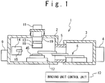
- the bonding unit control unit 10 is used for a bonding system. That is, the bonding system is provided with a bonding unit control unit 10 and a bonding unit 1.
- the bonding unit 1 is provided with a bonding chamber 2 and a load lock chamber 3.
- the bonding chamber 2 and the load lock chamber 3 are containers which shield the internal spaces of the chambers from environment.
- the bonding unit 1 is provided with a gate valve 5.
- the gate valve 5 is interposed between the bonding chamber 2 and the load lock chamber 3.
- the gate valve 5 is opened or closed to connect the internal space of the bonding chamber 2 and the internal space of the load lock chamber 3, through the control by the bonding unit control unit 10.
- the load lock chamber 3 is provided with a lid (not shown). The lid closes or opens a gate which connects the internal space of the load lock chamber 3 with the outside.
- the load lock chamber 3 is provided with a vacuum pump 4.
- the vacuum pump 4 is controlled by the bonding unit control unit 10 to exhaust gas from the internal space of the load lock chamber 3.
- the vacuum pump 4 a turbo-molecular pump, a cryopump, and an oil diffusion pump are exemplified.
- the load lock chamber 3 is provided with a conveyance mechanism 6 therein.
- the conveyance mechanism 6 is controlled by the bonding unit control unit 10 to convey a wafer or a substrate arranged in the load lock chamber 3 through the gate valve 5 to the bonding chamber 2, or to convey the wafer arranged in the bonding chamber 2 through the gate valve 5 into the internal space of the load lock chamber 3.
- the bonding chamber 2 is provided with a vacuum pump 9.
- the vacuum pump 9 is controlled by the bonding unit control unit 10 to exhaust gas from the internal space of the bonding chamber 2.
- a turbo-molecular pump, a cryopump, and an oil diffusion pump are exemplified.
- the bonding chamber 2 is provided with a stage cartridge 45 and a positioning mechanism 12.
- the stage cartridge 45 is arranged inside the bonding chamber 2 and is supported to be movable in a horizontal direction and rotatable around a rotation axis parallel to a vertical direction.
- the positioning mechanism 12 is controlled by the bonding unit control unit 10, to drive the stage cartridge 45 such that the stage cartridge 45 moves in the horizontal direction and rotates around the rotation axis parallel to the vertical direction.
- the bonding chamber 2 is provided with a pressure bonding mechanism 11, a pressure bonding axis 13, an electrostatic chuck 18 and a load meter 19.
- the pressure bonding axis 13 is supported to be movable in parallel to the vertical direction with respect to the bonding chamber 2.
- the electrostatic chuck 18 is arranged in the bottom end of the pressure bonding axis 13 and is provided with a dielectric layer on the surface opposite to the positioning mechanism 12.
- the electrostatic chuck 18 is controlled by the bonding unit control unit 10 to hold a wafer by electrostatic force.
- the pressure bonding mechanism 11 is controlled by the bonding unit control unit 10 to move the pressure bonding axis 13 in parallel to the vertical direction with respect to the bonding chamber 2.
- the pressure bonding mechanism 11 measures a position of the electrostatic chuck 18, and outputs the measured position to the bonding unit control unit 10.
- the load meter 19 measures the load applied to the wafer held by the electrostatic chuck 18 by measuring the load applied to the pressure bonding axis 13, and outputs the measured load to the bonding unit control unit 10.
- the bonding chamber 2 is provided with an ion gun 14 and an electron source 15.
- the ion gun 14 is arranged to turn to a space between the positioning mechanism 12 and the electrostatic chuck 18 when the electrostatic chuck 18 is arranged in an upper position.
- the ion gun 14 is controlled by the bonding unit control unit 10 to emit and accelerate argon ions along an irradiation axis which passes through the space between the positioning mechanism 12 and the electrostatic chuck 18 and intersects with the inner wall of the bonding chamber 2.
- the ion gun 14 is provided with metal targets (not shown). The metal target is arranged in the position to which the argon ions are irradiated.
- the metal target can be omitted.
- the electron source 15 is arranged to turn to the space between the positioning mechanism 12 and the electrostatic chuck 18.
- the electron source 15 is controlled by the bonding unit control unit 10 to emit and accelerate the electrons along another irradiation axis which passes through the space between the positioning mechanism 12 and the electrostatic chuck 18 and intersects the inner wall of the bonding chamber 2.
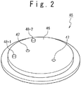
- FIG. 2 shows the stage cartridge 45.
- the stage cartridge 45 is formed to have an almost disk-like shape.
- the stage cartridge 45 is arranged so that a perpendicular axis of the disk-like shape is parallel to the vertical direction, and a flat support surface 46 is formed on the upper-side surface of the disk-like shape.
- a plurality of alignment holes 47 are formed in the support surface 46.
- a plurality of positioning pins 48-1 to 48-2 are formed in a peripheral region of the support surface 46.
- the plurality of positioning pins 48-1 to 48-2 are circular and are formed as tapered prominences.
- FIG. 3 shows a hand 17 provided for the conveyance mechanism 6.
- the hand 17 has nails 21-1 and 21-2.
- the nails 21-1 and 21-2 are respectively formed to have a tabular shape.
- the nails 21-1 and 21-2 are arranged in a horizontal plane.
- the nail 21-1 has a side edge 25-1 extending in a straight line
- the nail 21-2 has a side edge 25-2 extending in a straight line.
- the nails 21-1 and 21-2 are arranged such that the side edge 25-1 opposes to the side edge 25-2, and the side edge 25-1 and the side edge 25-2 are parallel.
- a cutout 49-1 is formed at a part of the side edge 25-1.
- a cutout 49-2 is formed at a part of the side edge 25-2.
- the cutout 49-1 and the cutout 49-2 are formed to be opposite to each other.
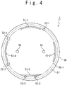
- FIG. 4 shows an upper-side cartridge 7.
- the upper-side cartridge 7 is formed of aluminum or stainless steel, is formed to have an almost disk-like shape, and is used to put an upper-side wafer.
- a plurality of positioning holes 53-1 and 53-2 and a plurality of alignment holes 54 are formed in the upper-side cartridge 7.
- the plurality of positioning holes 53-1 and 53-2 are formed to be circular and are formed in the neighborhood to the outer circumference of the disk-like shape.
- the diameter of the plurality of positioning holes 53-1 and 53-2 is substantially equal to the diameter of the positioning pins 48-1 to 48-2 of the stage cartridge 45, respectively.
- the plurality of positioning holes 53-1 and 53-2 are formed so that the distance between the positioning hole 53-1 and positioning hole 53-2 is same as the distance between the positioning pin 48-1 and the positioning pin 48-2. That is, the plurality of positioning holes 53-1 and 53-2 are arranged to engage with plurality of positioning pins 48-1 to 48-2 when the upper-side cartridge 7 is put on the stage cartridge 45. That is, when being placed on the stage cartridge 45 so that the plurality of positioning pins 48-1 to 48-2 are engaged with the plurality of positioning holes 53-1 and 53-2, the upper-side cartridge 7 is specified on a predetermined position of the stage cartridge 45.
- the plurality of alignment holes 54 are formed to pass through the upper-side cartridge 7.
- the plurality of alignment holes 54 are formed to be connected with the plurality of alignment holes 47 of the stage cartridge 45, respectively.
- the plurality of alignment holes 54 are formed to fit to alignment marks formed on the wafer.
- the upper-side cartridge 7 is provided with a plurality of island portions 51-1 to 51-4 and a plurality of wafer positioning pins 52-1 to 52-3 on the upper-side surface of a disk-like shape.
- the plurality of island portions 51-1 to 51-4 are formed as prominences which protrude from the upper-side surface of the disk-like shape, so as their upper ends to be in a same plane, and are formed to match the outer periphery of the wafer to be put on the upper-side cartridge 7.
- the plurality of wafer positioning pins 52-1 to 52-3 are formed as prominences which protrude from the upper-side surface of the disk-like shape and are formed to match the outer periphery of the wafer to be put on the upper-side cartridge 7.
- the wafer positioning pins 52-2 and 52-3 are formed to match the orientation flat of the wafer to be put on the upper-side cartridge 7.
- the orientation flat of the wafer contacts the wafer positioning pins 52-2 and 52-3, and the outer circumference of the wafer contacts the wafer positioning pin 52-1.
- the plurality of island portions 51-1 to 51-4 is formed such that passages connect a space between the upper-side cartridge 7 and the upper-side wafer with the outside. That is, the plurality of island portions 51-1 to 51-4 are formed not to be continuous.
- the plurality of wafer positioning pins 52-1 to 52-3 are formed higher than the plurality of island portions 51-1 to 51-4 and are formed lower than a summation of the height of plurality of island portions 51-1 to 51-4 and the thickness of the wafer. That is, as shown in FIG. 5 , the plurality of island portions 51-1 to 51-4 are formed to contact the outer periphery section of the lower-side surface of the upper-side wafer on the side of the upper-side cartridge 7 when the upper-side wafer is put on the upper-side cartridge 7.
- the plurality of wafer positioning pins 52-1 to 52-3 are formed to contact the side surface of the upper-side wafer when the upper-side wafer is put on the upper-side cartridge 7.
- the plurality of wafer positioning pins 52-1 to 52-3 are formed not to protrude from the upper-side surface of the upper-side wafer on the opposite side to the upper-side cartridge 7 when the upper-side wafer is put on the upper-side cartridge 7.
- the upper-side cartridge 7 is formed from a flange section 56 and a body section 57.
- the body section 57 is formed to have a column-like shape.
- the diameter of the column-like shape is smaller than the distance between the side edge 25-1 and the side edge 25-2 in the hand 17.
- the flange section 56 is formed to project from the side of the column-like shape of the body section 57 and is formed to have a disk-like shape.
- the diameter of the disk-like shape is larger than the distance between the side edge 25-1 and side edge 25-2 in the hand 17. That is, because the flange section 56 is put on the nails 21-1 and 21-2, the upper-side cartridge 7 is held by the conveyance mechanism 6.
- positioning pins 59 are further provided for the upper-side cartridge 7.
- the positioning pin 59 is formed as a prominence which protrudes from the lower-side surface of the flange section 56.
- the diameter of the positioning pin 59 is almost equal to the diameter of each of the cutouts 49-1 to 49-2.
- the two positioning pins 59 are formed in two symmetrical points with respect to the center of the disk of the flange section 56. That is, the positioning pins 59 are formed to be respectively engaged with the cutouts 49-1 and 49-2 of the nails 21-1 and 21-2 when the upper-side cartridge 7 is held by the conveyance mechanism 6. At this time, when being held by the conveyance mechanism 6 to be respectively fitted with the cutouts 49-1 and 49-2 of the nails 21-1 and 21-2, the upper-side cartridge 7 is held in a predetermined position of the hand 17.
- FIG. 8 shows a lower-side cartridge 8.
- the lower-side cartridge 8 is formed of aluminum or stainless steel, is formed to have an almost disk-like shape, and is used to put a lower-side wafer.
- a plurality of positioning holes 63-1 and 63-2 and a plurality of alignment holes 64 are provided for the lower-side cartridge 8.
- the plurality of positioning holes 63-1 and 63-2 are formed to be circular and are formed in the neighborhood to the outer periphery of the disk-like shape.
- the diameter of the plurality of positioning holes 63-1 and 63-2 is substantially equal to the diameter of the positioning pins 48-1 and 48-2 of the stage cartridge 45, respectively.
- the plurality of positioning holes 63-1 and 63-2 are formed such that a distance between the positioning hole 63-1 and the positioning hole 63-2 is equal to the distance between the positioning pin 48-1 and the positioning pin 48-2. That is, the plurality of positioning holes 63-1 to 63-2 are arranged to be engaged with the plurality of positioning pins 48-1 to 48-2 when the lower-side cartridge 8 is put on the stage cartridge 45. That is, when the lower-side cartridge 8 is arranged on the stage cartridge 45 such that the plurality of positioning pins 48-1 and 48-2 are engaged with the plurality of positioning holes 63-1 and 63-2, the lower-side cartridge 8 is put on a predetermined position of the stage cartridge 45.
- the plurality of alignment holes 64 are formed to pass through the lower-side cartridge 8.
- the plurality of alignment holes 64 are formed to be connected with the holes 47 of the stage cartridge 45 for the plurality of alignment marks, respectively, when the lower-side cartridge 8 is put on the stage cartridge 45.
- the plurality of alignment holes 64 are formed to match an alignment mark formed on the lower-side wafer when the lower-side wafer is put on the lower-side cartridge 8.
- the lower-side cartridge 8 is provided with island portions 61 and a plurality of wafer positioning pins 62-1 to 62-3 on the upper-side surface of the disk-like shape.
- the island sections 61 are formed as prominences which protrude from the upper-side surface of the disk such that the upper ends of the prominences are in a plane, and are formed to have the almost same shape of a wafer to be put on the lower-side cartridge 8.
- the island portions 61 are separated by grooves 65 in the upper end of the island portions 61.
- the grooves 65 are formed in a grid manner in the upper end of the island portions 61.
- the grooves 65 are formed to extend the side surface of the island portions 61.
- the plurality of wafer positioning pins 62-1-62-3 are formed as prominences which protrude from the upper-side surface of the disk-like shape and are formed to contact the outer periphery of the wafer to be put on the lower-side cartridge 8.
- the wafer positioning pins 62-2 and 62-3 are formed to contact the orientation flat of the wafer to be put on the lower-side cartridge 8. At this time, when the lower-side wafer is put on the lower-side cartridge 8 such that the orientation flat contacts the wafer positioning pins 62-2 and 62-3 and the side of the outer periphery of the wafer contacts the wafer positioning pin 62-1, the lower-side wafer is put in a predetermined position of the lower-side cartridge 8.
- the plurality of wafer positioning pins 62-1 to 62-3 are formed higher than the island portions 61 and are formed lower than a summation of the height of island portions 61 and the thickness of the wafer. That is, when the lower-side wafer is put on the lower-side cartridge 8, the island sections 61 are formed to contact most of the lower-side surface of the wafer on the side of the cartridge 8.
- the plurality of wafer positioning pins 62-1 to 62-3 are formed to contact the side of the lower-side wafer when the lower-side wafer is put on the lower-side cartridge 8.
- the plurality of wafer positioning pins 62-1 to 62-3 are formed not to protrude from the upper-side surface of the lower-side wafer when the lower-side wafer is put on the lower-side cartridge 8.
- the lower-side cartridge 8 is formed from a flange section 66 and a body section 67.
- the body section 67 is formed to have a column-like shape.
- the diameter of the column is smaller than a distance between the side edge 25-1 and the side edge 25-2.
- the flange section 66 is formed to project from the side of the column-like shape of the body section 67 and is formed to have a disk-like shape.
- the diameter of the disk is larger than the distance between the side edge 25-1 and the side edge 25-2. That is, because the flange section 66 is put on the nails 21-1 and 21-2, the lower-side cartridge 8 is held by the conveyance mechanism 6.
- the lower-side cartridge 8 is provided with positioning pins.
- the positioning pins are formed as prominences which protrude from the lower-side surface of the flange section 66.
- the diameter of the positioning pin is substantially equal to the diameter of the cutouts 49-1 and 49-2.
- the two positioning pins are formed on two symmetrical positions with respect to the center of the disk of the flange section 66. That is, the positioning pins are formed to engage with the cutouts 49-1 and 49-2 of the nails 21-1 and 21-2, respectively, when the lower-side cartridge 8 is held by the conveyance mechanism 6. At this time, when being held by the conveyance mechanism 6 to be respectively engaged with the cutouts 49-1 and 49-2 of the nails 21-1 and 21-2, the lower-side cartridge 8 is held in a predetermined position of the hand 17.
- the bonding unit 1 is further provided with two alignment mechanisms 91-1 and 91-2.
- the alignment mechanism 91-1 and 91-2 are arranged outside the bonding chamber 2 and are arranged on the opposite side of the electrostatic chuck 18 with respect to the stage cartridge 45.
- Each of the alignment mechanisms 91-1 and 91-2 is provided with a light source 92, a tube framework 93 and a camera 94.
- the light source 92, the tube framework 93 and the camera 94 are fixed on the bonding chamber 2.
- the light source 92 is controlled by the bonding unit control unit 10 to generate infrared rays which penetrate into a silicon substrate. As the wavelength of the infrared rays, an equal to or more than 1- ⁇ m wavelength is exemplified.
- the tube framework 93 changes the direction of the infrared rays which are generated by the light source 92, into a vertical direction and irradiates the infrared rays for the plurality of alignment holes 47 of the stage cartridge 45. Moreover, the tube framework 93 conducts the infrared rays emitted from the plurality of alignment holes 47 of the stage cartridge 45 for the tube framework 93 into the camera 94.
- the camera 94 is controlled by the bonding unit control unit 10, to generate an image from the infrared rays which passes through the tube framework 93 and output an electrical signal showing the image to the bonding unit control unit 10.
- FIG. 11 shows the bonding unit control unit 10.
- the bonding unit control unit 10 is provided with a CPU, a storage, a removable memory drive, an input unit and an interface (which are not shown).
- the CPU executes a computer program which is installed in the bonding unit control unit 10 and controls the storage, the input unit and the interface.
- the storage stores a computer program and temporarily stores data which are generated by the CPU.
- the removable memory drive is used to read the data which has been stored in a storage medium when the storage medium is inserted. Especially, the removable memory drive is used to install the computer program in the bonding unit control unit 10 when the storage medium in which the computer program has been stored is inserted.
- the input unit is operated by the user to generate data and outputs the data to the CPU.
- the interface outputs data generated by one of external units being connected with the bonding unit control unit 10, to the CPU, and outputs data generated by the CPU to the external unit.
- the external units contain the vacuum pump 4, the conveyance mechanism 6, the vacuum pump 9, the pressure bonding mechanism 11, the positioning mechanism 12, the ion gun 14, the electron source 15, the electrostatic chuck 18, the load meter 19, the light source 92 and the camera 94.
- the computer program which is installed in the bonding unit control unit 10 is formed from a plurality of computer program portions to make the bonding unit control unit 10 realize a plurality of functions.
- the plurality of functions contain a conveyance section 31, a driving section 32, a chuck control section 33, an activation section 34 and an alignment section 35.
- the conveyance section 31 closes the gate valve 5. Moreover, when the gate valve 5 is closed, the conveyance section 31 sets the load lock chamber 3 to a preliminary atmosphere with a predetermined vacuum degree inside by using the vacuum pump 4 or sets the load lock chamber 3 to an atmosphere with an atmospheric pressure. When the load lock chamber 3 is set to the atmosphere with the preliminary vacuum degree, the conveyance section 31 opens or closes the gate valve 5. When the gate valve 5 is open, the conveyance section 31 conveys the stage cartridge 45 which is arranged inside the load lock chamber 3 to the positioning mechanism 12 by using the conveyance mechanism 6 or conveys the stage cartridge 45 which is held by the positioning mechanism 12, into the load lock chamber 3 by using the conveyance mechanism 6.
- the driving section 32 controls the pressure bonding mechanism 11 so as to move the electrostatic chuck 18 in parallel. Moreover, the driving section 32 calculates a timing at which the electrostatic chuck 18 reaches a predetermined position, and controls the pressure bonding mechanism 11 to stop the electrostatic chuck 18 at the timing. The driving section 32 calculates the timing that the load measured by the load meter 19 reaches a predetermined load, and controls the pressure bonding mechanism 11 to stop the electrostatic chuck 18 at the timing.
- the chuck control section 33 controls the electrostatic chuck 18 to hold a wafer or not to hold the wafer.
- the activation section 34 sets the bonding chamber 2 to a bonding atmosphere with a predetermined vacuum degree by using the vacuum pump 9. Moreover, when the bonding chamber 2 is set to the bonding atmosphere, the activation section 34 controls the ion gun 14 to emit argon ions for a space between the upper-side wafer and the lower-side wafer. Moreover, while the argon ions are emitted, the activation section 34 controls the electron source 15 to emit electrons for the space between the upper-side wafer and the lower-side wafer.
- the alignment section 35 controls the positioning mechanism 12 such that the upper-side wafer is positioned in a predetermined horizontal position. Moreover, when the electrostatic chuck 18 holds an upper-side wafer and the lower-side cartridge 8 having the lower-side wafer thereon is located on the stage cartridge 45, the alignment section 35 controls the pressure bonding mechanism 11 to bring the upper-side wafer close to the lower-side wafer up to a predetermined distance. Moreover, the alignment section 35 controls the positioning mechanism 12 to set the lower-side wafer to a horizontal position for the upper-side wafer when the upper-side wafer and the lower-side wafer are brought close to each other up to the predetermined distance.
- the bonding method according to the embodiment of present invention includes an operation performed by using the bonding unit 1 and an operation performed without using the bonding unit 1.
- FIG. 12 shows the operation performed by using the bonding unit 1.
- An operator first closes the gate valve 5, and then sets the bonding chamber 2 to a vacuum atmosphere by using the vacuum pump 9 and the load lock chamber 3 to an atmosphere with the atmospheric pressure.
- the operator puts an upper-side wafer on the upper-side cartridge 7 such that the orientation flat of the upper-side wafer contacts the wafer positioning pins 52-2 and 52-3 and the side of the outer periphery of the upper-side wafer contacts the wafer positioning pin 52-1.
- the operator puts the lower-side wafer on the lower-side cartridge 8 such that the orientation flat of the lower-side wafer contact the wafer positioning pins 62-2 and 62-3, and the side of the outer periphery of the lower-side wafer contacts the wafer positioning pin 62-1.
- a plurality of the lower-side cartridges 8 with the lower-side wafers are prepared.
- the operator opens the lid of the load lock chamber 3, and arranges the upper-side cartridge 7 in the load lock chamber 3 and arranges the plurality of lower-side cartridges 8 in the load lock chamber 3.
- the operator closes the lid of the load lock chamber 3 and sets the load lock chamber 3 to the vacuum atmosphere.
- the bonding unit control unit 10 opens the gate valve 5 after the load lock chamber 3 is set to the vacuum atmosphere.
- the bonding unit control unit 10 first controls the electrostatic chuck 18 to hold the upper-side wafer.
- the bonding unit control unit 10 controls the conveyance mechanism 6 to convey the upper-side cartridge 7 with the upper-side wafer put, from the load lock chamber 3 to the stage cartridge 45.
- the bonding unit control unit 10 controls the conveyance mechanism 6 to move down the hand 17 of the conveyance mechanism 6.
- the upper-side cartridge 7 is held by the stage cartridge 45 by engaging the plurality of positioning holes 53-1 and 53-2 with the plurality of positioning pins 48-1 to 48-2 of the stage cartridge 45, respectively (Step S1).
- the bonding unit control unit 10 controls the conveyance mechanism 6 to draw back the hand 17 of the conveyance mechanism 6 into the load lock chamber 3.
- the bonding unit control unit 10 controls the alignment mechanisms 91-1 and 91-2 to pickup images of the alignment marks formed on the upper-side wafer.
- the bonding unit control unit 10 controls the positioning mechanism 12 based on the images such that the upper-side wafer is positioned in the predetermined horizontal position (Step S2).
- the bonding unit control unit 10 controls the pressure bonding mechanism 11 to move the electrostatic chuck 18 down into the vertical direction.
- the bonding unit control unit 10 controls the pressure bonding mechanism 11 to stop the electrostatic chuck 18 when the electrostatic chuck 18 contacts the upper-side wafer, and controls the electrostatic chuck 18 to hold an upper-side wafer.
- the bonding unit 1 can make the electrostatic chuck 18 contact the upper-side wafer more surely and can make the electrostatic chuck 18 hold the upper-side wafer more surely.
- the bonding unit control unit 10 controls the pressure bonding mechanism 11 such that the upper-side wafer leaves the upper-side cartridge 7, that is, the electrostatic chuck 18 rise upwardly.
- the bonding unit control unit 10 controls the conveyance mechanism 6 to draw back the upper-side cartridge 7 with no upper-side wafer from the stage cartridge 45 into the load lock chamber 3 after the upper-side wafer leaves the upper-side cartridge 7 (Step S3).
- the bonding unit control unit 10 controls the conveyance mechanism 6 to convey the cartridge 8 with the lower-side wafer put from the load lock chamber 3 to the stage cartridge 45 after the electrostatic chuck 18 holds the upper-side wafer.
- the bonding unit control unit 10 controls the conveyance mechanism 6 to move down the hand 17 of the conveyance mechanism 6.
- the lower-side cartridge 8 is held by the stage cartridge 45 such that the plurality of positioning holes 63-1 and 63-2 are engaged with the plurality of positioning pins 48-1 and 48-2 of the stage cartridge 45, respectively.
- the bonding unit control unit 10 controls the conveyance mechanism 6 to draw back the hand 17 of the conveyance mechanism 6 into the load lock chamber 3.
- the bonding unit control unit 10 closes the gate valve 5 and controls the vacuum pump 9 to vacuum the bonding chamber 2 to the bonding atmosphere with a predetermined vacuum degree (Step S4).
- the bonding unit control unit 10 controls alignment mechanisms 91-1 and 91-2 to pick up images of the alignment marks formed on the lower-side wafer.
- the bonding unit control unit 10 controls the positioning mechanism 12 based on the images to position the lower-side wafer to a predetermined horizontal position (Step S5).
- the bonding unit control unit 10 controls the ion gun 14 to emit particles for a space between the upper-side wafer and the lower-side wafer in a state which the upper-side wafer held by the electrostatic chuck 18 is apart from the lower-side wafer held by the stage cartridge 45 (Step S6).
- the particles are irradiated to the upper-side wafer and the lower-side wafer to remove oxide films formed on the surfaces and removes impurities adhered to the surfaces.
- the bonding unit control unit 10 controls the pressure bonding mechanism 11 to move down the electrostatic chuck 18 to a predetermined position downwardly into the vertical direction.
- the bonding unit control unit 10 controls the pressure bonding mechanism 11 such that the upper-side wafer and the lower-side wafer leave from each other by a predetermined distance, that is, the electrostatic chuck 18 stops at a predetermined position (Step S7).
- the bonding unit control unit 10 controls the alignment mechanisms 91-1 and 91-2 such that the images of the alignment marks formed on the upper-side wafer and the alignment marks formed on the lower-side wafer are picked up.
- the bonding unit control unit 10 controls the positioning mechanism 12 based on the images of the upper-side wafer and the lower-side wafer, so as to be bonded according to design (Step S9) .
- the bonding unit control unit 10 controls the pressure bonding mechanism 11 such that the bonded upper-side wafer contact the other lower-side wafer, that is, the electrostatic chuck 18 moves down downwardly into the vertical direction (Step S12).
- the upper-side wafer and the lower-side wafer are bonded through the contact of them and one sheet of bonded wafer is generated.
- the bonding unit 1 can make the upper-side wafer contact the lower-side wafer more surely and can bond the upper-side wafer and the lower-side wafer more surely. Moreover, at this time, the island portions 61 of the lower-side cartridge 8 contact most of all the part of the lower-side wafer. Therefore, the lower-side wafer can be prevented from damage due to the load which is applied in the bonding. Also, the bonding unit 1 can apply a larger load on the upper-side wafer and the lower-side wafer.
- the bonding unit control unit 10 controls the electrostatic chuck 18 to leave the bonding wafer from the lower-side cartridge 8, that is, to continue to hold the bonded wafer, and controls the pressure bonding mechanism 11 such that the electrostatic chuck 18 rises upwardly to the vertical direction.
- the bonding unit control unit 10 opens the gate valve 5, and controls the conveyance mechanism 6 to draw back the lower-side cartridge 8 from the stage cartridge 45 into the load lock chamber 3.
- the bonding unit control unit 10 controls the conveyance mechanism 6 to convey the lower-side cartridge 8 with a lower-side wafer from the load lock chamber 3 to the stage cartridge 45.
- the bonding unit control unit 10 controls the conveyance mechanism 6 to move down the hand 17 of the conveyance mechanism 6. At this time, the plurality of positioning holes 63-1 and 63-2 are engaged with the plurality of positioning pins 48-1 to 48-2 of the stage cartridge 45, respectively, so that the lower-side cartridge 8 is held by the stage cartridge 45.
- the bonding unit control unit 10 controls the conveyance mechanism 6 to draw back the hand 17 of the conveyance mechanism 6 into the load lock chamber 3.
- the bonding unit control unit 10 closes the gate valve 5 and controls the vacuum pump 9 to vacuum the bonding chamber 2 to the bonding atmosphere with a predetermined vacuum degree (Step S13).
- the bonding unit control unit 10 controls the alignment mechanisms 91-1 and 91-2 to pick up images of the alignment marks formed on the lower-side wafer.
- the bonding unit control unit 10 controls the positioning mechanism 12 based on the images to position the lower-side wafer in a predetermined horizontal position of (Step S5).
- the bonding unit control unit 10 controls the ion gun 14 to emit particles to a space between the bonded wafer and the lower-side wafer in a state that the bonded wafer held by the electrostatic chuck 18 is separated from the wafer held by the stage cartridge 45 (Step S6).
- the particles are irradiated to the bonded wafer and the lower-side wafer to remove oxide films formed on the surfaces and remove impurities adhered to the surfaces.
- the bonding unit control unit 10 controls the pressure bonding mechanism 11 to move down the electrostatic chuck 18 to a predetermined position downwardly into the vertical direction.
- the bonding unit control unit 10 controls the pressure bonding mechanism 11 such that the bonded wafer is separated from the lower-side wafer by a predetermined distance, that is, the electrostatic chuck 18 stops at a predetermined position (Step S7).
- the bonding unit control unit 10 controls the alignment mechanisms 91-1 and 91-2 such that the images of the alignment marks formed on the bonded wafer and the alignment marks formed on the lower-side wafer are picked up.
- the bonding unit control unit 10 controls the positioning mechanism 12 based on the images of the bonded wafer and the lower-side wafer so as to be bonded according to the design (Step S9).
- the bonding unit control unit 10 controls the pressure bonding mechanism 11 such that the bonded wafer contacts the lower-side wafer, that is, the electrostatic chuck 18 moves down downwardly in the vertical direction. The bonded wafer and the lower-side wafer are bonded through the contact and one sheet of the bonded wafer is generated. Moreover, the bonding unit control unit 10 controls the electrostatic chuck 18 to dechuck the bonded wafer from the electrostatic chuck 18 (Step S14) .
- the bonded wafer produced at step S12 can be more bonded with another wafer without being taken out from the bonding chamber 2. Therefore, according to such an operation, three or more wafers can be bonded at higher speed as compared with a case that a couple of wafers are bonded, and three or more wafers can be bonded at a low cost.
- the bonding unit control unit 10 controls the pressure bonding mechanism 11 to raise the electrostatic chuck 18 upwardly in the vertical direction.
- the bonding unit control unit 10 opens the gate valve 5, and controls the conveyance mechanism 6 to convey the cartridge 8 with the bonded wafer put from the stage cartridge 45 to the load lock chamber 3.
- the bonding unit control unit 10 closes the gate valve 5 and controls the vacuum pump 4 to set the load lock chamber 3 to atmosphere with an atmospheric pressure.
- the operator opens the lid of the load lock chamber 3 after the atmospheric-pressure atmosphere is set inside the load lock chamber 3, and takes out the bonded wafer (Step S15).
- the operator prepares three cartridges (cartridges 81, 83, and 85).
- the operator puts the wafer 82 on the cartridge 81, puts the wafer 84 on the cartridge 83 and puts the wafer 86 on the cartridge 85.
- the cartridge 81 the upper-side cartridge 7 is exemplified.
- the cartridge 83 the lower-side cartridge 8 is exemplified.
- the cartridge 85 the lower-side cartridge 8 is exemplified.
- step S1 the cartridge 81 with the wafer 82 put is set on the stage cartridge 45 and the electrostatic chuck 18 absorbing nothing is arranged in a position apart from the stage cartridge 45.
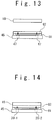
- step S3 as shown in FIG. 14 , the wafer 82 put on the cartridge 81 which has been put on the stage cartridge 45 contacts the electrostatic chuck 18 and the wafer 82 is sucked by the electrostatic chuck 18.
- step S3 As shown in FIG. 15 , after step S3 is executed, the cartridge 81 with no wafer is put on the stage cartridge 45 and the electrostatic chuck 18 on which the wafer 82 has been sucked is arranged in a position the stage cartridge 45.
- step S4 the cartridge 83 on which the wafer 84 is put is put on the stage cartridge 45, and the electrostatic chuck 18 by which the wafer 82 has been absorbed is arranged in a position apart from the stage cartridge 45.
- step S12 the wafer 84 put on the cartridge 83 contacts the wafer 82 sucked by the electrostatic chuck 18.
- step S12 the bonded wafer 87 is formed from the wafer 84 and the wafer 82, and the cartridge 83 with no wafer is put on the stage cartridge 45.
- the electrostatic chuck 18 by which a bonded wafer 87 has been sucked is arranged in a position apart from the stage cartridge 45.
- step S13 the cartridge 85 on which the wafer 86 has been put is put on the stage cartridge 45 and the electrostatic chuck 18 by which the bonded the wafer 87 has been sucked is arranged in a position apart from the stage cartridge 45.
- step S14 is executed without executing the step S12. As shown in FIG. 20 , at the step S14, the wafer 86 put on the cartridge 85 contacts the bonded wafer 87 sucked by the electrostatic chuck 18.
- a bonded wafer 88 is formed from the bonded wafer 87 and the wafer 86.
- the cartridge 85 on which the bonded wafer 88 is put is located on the stage cartridge 45.
- the electrostatic chuck 18 with no wafer is arranged in a position apart from the stage cartridge 45.
- the bonded wafer 87 formed from the wafer 82 and the wafer 84 can be bonded with the wafer 86 without being taken out from the bonding chamber 2. Therefore, according to such an operation, three or more wafers can be bonded at higher speed compared with the case that a couple of the wafers are bonded, and three or more wafers can be bonded at the low cost.
- the operation which is executed without using the bonding unit 1 includes an operation of producing a wafer which is a bonding object and an operation of dicing the bonded wafer.
- the upper-side wafer and the lower-side wafer are produced, e.g. the wafers 82, 84 and 86 shown in FIG. 13 to FIG. 21 are produced.
- the bonded wafer produced by bonding two wafers by using the bonding unit 1 can be applied as the wafer 84 or the wafer 86.
- the wafer obtained by processing the bonded wafer can be applied as the wafer 84 or the wafer 86. If such a wafer is applied as the wafer 84 or the wafer 86,
- the plurality of wafers can be bonded such that an order where a plurality of bonding surfaces are arranged and an order that the plurality of bonding surfaces are bonded are different from each other. Thus, it is possible to diversify in the form of the bonding.
- the bonded wafer formed by using the bonding unit 1 is divided into a plurality of devices. That is, the operation which is executed by using the bonding unit 1 is suitable for producing the bonded wafer which is divided into the plurality of devices.
- a wafer 70 which is exemplified by the upper-side wafer and the lower-side wafer is sometimes transformed as shown in FIG. 22 .
- a space 72 is formed between the wafer 70 and the cartridge 71.
- the air filling the space 72 lifts the wafer 70 and sometimes moves the wafer 70 along the surface of the cartridge 71 if the atmosphere where the wafer 70 and the cartridge 71 are arranged is decompressed, when there is no passage which connects the space 72 and the outside.
- the gas filling the space between the upper-side cartridge 7 and the upper-side wafer is exhausted outside through passages between the plurality of island portions 51-1 to 51-4. Such exhaustion prevents the gas between the upper-side cartridge 7 and the upper-side wafer from lifting the upper-side wafer and prevents the upper-side wafer from moving on the upper-side cartridge 7. Moreover, the gas filling the space between the lower-side cartridge 8 and the lower-side wafer is exhausted outside through the grooves 65 as passages. Such exhaustion prevents the between the lower-side cartridge 8 and the lower-side wafer from lifting the lower-side wafer and prevents the lower-side wafer from moving on the lower-side cartridge 8.
- a multi-layer bonding method of bonding according to the present invention may be executed by using another bonding unit in which the alignment mechanisms 91-1 and 91-2 are arranged in other positions.
- the positions which are nearer to the electrostatic chuck 18 than the positioning mechanism 12, for example, the upper positions of the electrostatic chuck 18 are exemplified.
- the multi-layer bonding method of according to the present invention can bond three or more wafers at higher speed even when being applied to such a bonding unit, like the above embodiments.
- steps S2, S5, S7 and S9 in the embodiments are omitted.
- Such a multi-layer bonding method can be applied when high accuracy alignment is unnecessary.
- three or more wafers can be bonded at higher speed and at a low cost.
- the conveyance mechanism 6 in the above embodiments directly contacts and conveys the wafer and the stage cartridge 45 directly contacts the wafer and holds the wafer.
- three or more wafers can be bonded at higher speed, like the above embodiments.
- the recovery of the cartridge is unnecessary.
- Three or more wafers can be bonded at higher speed, as compared with the above embodiments.
- the cartridge is unnecessary and three or more wafers can be bonded at the low cost.
- the wafer conveyed into the bonding chamber 2 by the conveyance mechanism 6 is transferred to the electrostatic chuck 2 in the air without being supported by the stage cartridge 45 and is held by the electrostatic chuck 2.
- the wafer held by the electrostatic chuck 2 is bonded by another wafer supported on the stage cartridge 45.
- the bonded wafer is supported on the stage cartridge 45, still another wafer is held by the electrostatic chuck 2 in the same way and the bonded wafer and the wafer held by the electrostatic chuck 2 are bonded.
- a multi-layer bonding method three or more wafers can be bonded at a low cost, like the multi-layer bonding method in the above embodiment.
- the multi-layer bonding method according to the present invention can be applied to another bonding unit in which two wafers are brought into contact and bonded by moving the wafers into a direction which is different from the vertical direction.
- a horizontal direction is exemplified.
- three or more wafers can be bonded at a higher speed when being applied to such a bonding unit, like the above embodiments.
Landscapes
- Engineering & Computer Science (AREA)
- Manufacturing & Machinery (AREA)
- Microelectronics & Electronic Packaging (AREA)
- Mechanical Engineering (AREA)
- Pressure Welding/Diffusion-Bonding (AREA)
- Container, Conveyance, Adherence, Positioning, Of Wafer (AREA)
- Micromachines (AREA)
Claims (12)
- Ein Mehrschichtverbindungsverfahren mit:Ausbilden eines ersten verbundenen Substrats (87) durch Verbinden eines ersten Substrats (82) und eines Zwischensubstrats (84) in einer Verbindungskammer (2),Transportieren eines zweiten Substrats (86) in die Verbindungskammer (2), wenn das erste verbundene Substrat (87) im Inneren der Verbindungskammer (2) angeordnet ist, undAusbilden eines zweiten verbundenen Substrats (88) durch Verbinden des ersten verbundenen Substrats (87) mit dem zweiten Substrat (86) in der Verbindungskammer (2),dadurch gekennzeichnet, dassdas Zwischensubstrat (84) in die Verbindungskammer (2) in einem Zustand transportiert wird, bei dem das Zwischensubstrat (84) auf einer Zwischenkassette (83) angeordnet ist,wobei das erste Substrat (82) und das Zwischensubstrat (84) in dem Zustand verbunden werden, bei dem das Zwischensubstrat (84) auf der Zwischenkassette (83) angeordnet ist,wobei die Zwischenkassette (83) von der Verbindungskammer (2) in dem Zustand transportiert wird, bei dem das erste verbundene Substrat (87) nicht auf der Zwischenkassette (83) angeordnet ist, nachdem das erste Substrat (82) und das Zwischensubstrat (84) verbunden sind,wobei das zweite Substrat (86) in die Verbindungskammer (2) in einem Zustand transportiert wird, bei dem das zweite Substrat (86) auf einer Kassette (85) angeordnet ist, nachdem die Zwischenkassette (83) aus der Verbindungskammer (2) heraus transportiert wird, undwobei das erste verbundene Substrat (87) und das zweite Substrat (86) in dem Zustand verbunden werden, bei dem das zweite Substrat (86) auf der Kassette (85) angeordnet ist.
- Das Mehrschichtverbindungsverfahren gemäß Anspruch 1, wobei eine zwischen dem zweiten Substrat (86) und dem ersten verbundenen Substrat (87) aufgebrachte Last, wenn das zweite Substrat (86) und das erste verbundene Substrat (87) verbunden werden, größer ist als eine Last, die zwischen dem ersten Substrat (82) und dem Zwischensubstrat (84) aufgebracht wird, wenn das erste Substrat (82) und das Zwischensubstrat (84) verbunden werden.
- Das Mehrschichtverbindungsverfahren gemäß Anspruch 1 oder 2, ferner mit:Aktivieren gegenüberliegender Oberflächen des Zwischensubstrats (84) und des ersten Substrats (82), bevor das erste Substrat (82) und das Zwischensubstrat (84) verbunden werden, undAktivieren gegenüberliegender Oberflächen des zweiten Substrats (86) und des ersten verbundenen Substrats (87), bevor das erste verbundene Substrat (87) und das zweite Substrat (86) verbunden werden.
- Das Mehrschichtverbindungsverfahren gemäß einem der Ansprüche 1 bis 3, ferner mit:Ausrichten des ersten Substrats (82) und des Zwischensubstrats (84), bevor das erste Substrat (82) und das Zwischensubstrat (84) verbunden werden, undAusrichten des ersten verbundenen Substrats (87) und des zweiten Substrats (86), bevor das erste verbundene Substrat (87) das zweite Substrat (86) verbunden werden.
- Das Mehrschichtverbindungsverfahren gemäß einem der Ansprüche 1 bis 4, ferner mit:
Herstellen des Zwischensubstrats (84) durch Bearbeiten eines dritten verbundenen Substrats, das durch Verbinden von zwei Substraten hergestellt wurde. - Das Mehrschichtverbindungsverfahren gemäß einem der Ansprüche 1 bis 5, ferner mit:
Herstellen einer Vielzahl von Vorrichtungen durch Würfeln des zweiten verbundenen Substrats (88). - Das Mehrschichtverbindungsverfahren gemäß einem der Ansprüche 1 bis 6, ferner mit:Dekomprimieren eines internen Raums einer Lastverriegelungskammer (3), wenn die Kassette (85) in der Lastverriegelungskammer (3) angeordnet ist und das zweite Substrat (86) auf der Kassette (85) angeordnet ist,wobei das zweite Substrat (86) von der Lastverriegelungskammer (3) in die Verbindungskammer (2) transportiert wird, nachdem der interne Raum der Lastverriegelungskammer (3) dekomprimiert ist,wobei die Kassette (85) mit Inselabschnitten (61) versehen ist, welche das zweite Substrat (86) kontaktieren, wenn das zweite Substrat (86) auf der Kassette (85) angeordnet ist, undwobei Durchgänge (65) für die Inselabschnitte (61) vorgesehen sind, um einen Raum zwischen der Kassette (85) und dem zweiten Substrat (86) zu einer Außenseite zu verbinden, wenn das zweite Substrat (86) auf der Kassette (85) angeordnet ist.
- Eine Verbindungseinheit-Steuereinheit (10) mit:einem Antriebsabschnitt (32), der konfiguriert ist, um einen Druckverbindungsmechanismus (11) zum Verbinden eines ersten Substrats (82) und eines Zwischensubstrats (84) in einer Verbindungskammer (2) zu steuern, undeinem Transportabschnitt (31), der konfiguriert ist, um einen Transportmechanismus (6) zum Transportieren eines zweiten Substrats (86) in die Verbindungskammer (2) hinein zu steuern, wenn ein erstes verbundenes Substrat (87), das durch Verbinden des ersten Substrats (82) und des Zwischensubstrats (84) gebildet ist, in der Verbindungskammer (2) angeordnet ist bzw. wird,wobei der Antriebsabschnitt (32) konfiguriert ist, um den Druckverbindungsmechanismus (11) zum Verbinden des ersten verbundenen Substrats (87) und des zweiten Substrats (86) in der Verbindungskammer (2) zu steuern,dadurch gekennzeichnet, dassdas Zwischensubstrat (84) in die Verbindungskammer (2) hinein in einem Zustand transportiert wird, bei dem das Zwischensubstrat (84) auf einer Zwischenkassette (83) angeordnet ist,wobei das erste Substrat (82) und das Zwischensubstrat (84) in dem Zustand verbunden werden, bei dem das Zwischensubstrat (84) auf der Zwischenkassette (83) angeordnet ist,wobei die Zwischenkassette (83) von der Verbindungskammer (2) in einem Zustand heraus transportiert wird, bei dem das erste verbundene Substrat (87) nicht auf der Zwischenkassette (83) angeordnet ist, nachdem das erste Substrat (82) und das Zwischensubstrat (84) verbunden sind,wobei ein zweites Substrat (86) in die Verbindungskammer (2) in einem Zustand transportiert wird, bei dem das zweite Substrat (86) auf einer Kassette (85) angeordnet ist, nachdem die Zwischenkassette (83) aus der Verbindungskammer (2) heraus transportiert wird, undwobei das erste verbundene Substrat (87) und das zweite Substrat (86) in dem Zustand verbunden werden, bei dem das zweite Substrat (86) auf der Kassette (85) angeordnet ist.
- Die Verbindungseinheit-Steuereinheit (10) gemäß Anspruch 8, wobei der Antriebsabschnitt (32) konfiguriert ist, um den Druckverbindungsmechanismus (11) so anzutreiben, dass eine zwischen dem zweiten Substrat (86) und dem ersten verbundenen Substrat (87) aufgebrachte Last, wenn das zweite Substrat (86) und das erste verbundene Substrat (87) verbunden werden, größer ist als eine Last, die zwischen dem ersten Substrat (82) und dem Zwischensubstrat (84) aufgebracht wird, wenn das erste Substrat (82) und das Zwischensubstrat (84) verbunden werden.
- Die Verbindungseinheit-Steuereinheit (10) gemäß Anspruch 8 oder 9, ferner mit:einem Aktivierungsabschnitt (34), der konfiguriert ist, um eine Aktivierungseinheit (14) so zu steuern, dass gegenüberliegende Oberflächen des Zwischensubstrats (84) und des ersten Substrats (82) aktiviert werden, bevor das erste Substrat (82) und das Zwischensubstrat (84) verbunden werden,wobei der Antriebsabschnitt (32) konfiguriert ist, um die Aktivierungseinheit (14) so zu steuern, dass gegenüberliegende Oberflächen des zweiten Substrats (86) und des ersten verbundenen Substrats (87) aktiviert werden, bevor das erste verbundene Substrat (87) und das zweite Substrat (86) verbunden werden.
- Die Verbindungseinheit-Steuereinheit (10) gemäß einem der Ansprüche 8 bis 10, ferner mit:einem Ausrichtabschnitt (35), der konfiguriert ist, um einen Ausrichtmechanismus (91-1,91-2) zum Ausrichten des ersten Substrats (82) und des Zwischensubstrats (84) zu steuern, bevor das erste Substrat (82) und das Zwischensubstrat (84) verbunden werden,wobei der Ausrichtabschnitt (35) konfiguriert ist, um den Ausrichtmechanismus (91-1,91-2) zum Ausrichten des ersten verbundenen Substrats (87) und des zweiten Substrats (86) zu steuern, bevor das erste verbundene Substrat (87) und das zweite Substrat (86) verbunden werden.
- Die Verbindungseinheit-Steuereinheit (10) gemäß einem der Ansprüche 8 bis 11, wobei der Transportabschnitt (31) konfiguriert ist, um einen internen Raum einer Lastverriegelungskammer (3) zu dekomprimieren, wenn die Kassette (85) in der Lastverriegelungskammer (3) angeordnet ist und das zweite Substrat (86) auf der Kassette (85) angeordnet ist,
wobei der Transportabschnitt (31) konfiguriert ist, um den Transportmechanismus (6) so zu steuern, dass das zweite Substrat (86) von der Lastverriegelungskammer (3) in die Verbindungskammer (2) transportiert wird, nachdem der interne Raum der Lastverriegelungskammer (3) dekomprimiert ist bzw. wurde,
wobei Inselabschnitte (61) für die Kassette (85) vorgesehen sind, um das zweite Substrat (86) zu kontaktieren, wenn das zweite Substrat (86) auf der Kassette (85) angeordnet ist, und
wobei Durchgänge (85) für die Inselabschnitte (61) vorgesehen sind, um einen Raum zwischen der Kassette (85) und dem zweiten Substrat (86) zu einer Außenseite zu verbinden, wenn das zweite Substrat (86) auf der Kassette (85) angeordnet ist.
Applications Claiming Priority (2)
| Application Number | Priority Date | Filing Date | Title |
|---|---|---|---|
| JP2009247855A JP4831842B2 (ja) | 2009-10-28 | 2009-10-28 | 接合装置制御装置および多層接合方法 |
| PCT/JP2010/069039 WO2011052627A1 (ja) | 2009-10-28 | 2010-10-27 | 接合装置制御装置および多層接合方法 |
Publications (3)
| Publication Number | Publication Date |
|---|---|
| EP2495752A1 EP2495752A1 (de) | 2012-09-05 |
| EP2495752A4 EP2495752A4 (de) | 2015-05-06 |
| EP2495752B1 true EP2495752B1 (de) | 2018-07-25 |
Family
ID=43922052
Family Applications (1)
| Application Number | Title | Priority Date | Filing Date |
|---|---|---|---|
| EP10826759.2A Not-in-force EP2495752B1 (de) | 2009-10-28 | 2010-10-27 | Steuergerät für eine bindevorrichtung und mehrschichtbindungsverfahren |
Country Status (8)
| Country | Link |
|---|---|
| US (1) | US9064910B2 (de) |
| EP (1) | EP2495752B1 (de) |
| JP (1) | JP4831842B2 (de) |
| KR (1) | KR101295997B1 (de) |
| CN (1) | CN102414784B (de) |
| CA (1) | CA2758157C (de) |
| TW (1) | TWI540622B (de) |
| WO (1) | WO2011052627A1 (de) |
Families Citing this family (9)
| Publication number | Priority date | Publication date | Assignee | Title |
|---|---|---|---|---|
| TWI594966B (zh) * | 2010-10-08 | 2017-08-11 | Ohara Kk | Optical glass, preform and optical element |
| KR102009551B1 (ko) * | 2014-02-03 | 2019-08-09 | 에베 그룹 에. 탈너 게엠베하 | 기질을 결합하기 위한 방법 및 장치 |
| JP6874692B2 (ja) * | 2015-12-28 | 2021-05-19 | 株式会社ニコン | 基板貼り合わせ装置および基板貼り合わせ方法 |
| DE102017105697B4 (de) * | 2017-03-16 | 2025-12-31 | Ev Group E. Thallner Gmbh | Verfahren und System zur Ausrichtung zweier gegenüberliegend angeordneter optischer Teilsysteme und Kamerachip |
| JP7177781B2 (ja) * | 2017-03-16 | 2022-11-24 | エーファウ・グループ・エー・タルナー・ゲーエムベーハー | 少なくとも3枚の基板を接合するための方法 |
| TWI850225B (zh) * | 2018-04-12 | 2024-08-01 | 日商尼康股份有限公司 | 位置對準方法及位置對準裝置 |
| CN118763017A (zh) * | 2018-08-29 | 2024-10-11 | 东京毅力科创株式会社 | 接合装置的参数调整方法和接合装置 |
| KR102566141B1 (ko) | 2019-07-02 | 2023-08-11 | 삼성전자주식회사 | 웨이퍼 본딩 방법 및 웨이퍼 본딩 장치 |
| TWI732700B (zh) * | 2020-10-16 | 2021-07-01 | 天虹科技股份有限公司 | 鍵合機台的對準機構及對準方法 |
Family Cites Families (12)
| Publication number | Priority date | Publication date | Assignee | Title |
|---|---|---|---|---|
| JP2984441B2 (ja) | 1991-12-06 | 1999-11-29 | 光正 小柳 | 三次元lsi積層装置 |
| JP2701709B2 (ja) * | 1993-02-16 | 1998-01-21 | 株式会社デンソー | 2つの材料の直接接合方法及び材料直接接合装置 |
| US6390905B1 (en) * | 2000-03-31 | 2002-05-21 | Speedfam-Ipec Corporation | Workpiece carrier with adjustable pressure zones and barriers |
| DE10217097A1 (de) * | 2001-04-18 | 2002-11-21 | Denso Corp | Verfahren zur Herstellung eines keramischen Laminats |
| JP4575651B2 (ja) | 2003-06-04 | 2010-11-04 | 富士ゼロックス株式会社 | 積層構造体の製造方法および積層構造体 |
| JP2005026608A (ja) * | 2003-07-02 | 2005-01-27 | Tokyo Electron Ltd | 接合方法および接合装置 |
| JP2008288384A (ja) | 2007-05-17 | 2008-11-27 | Sony Corp | 3次元積層デバイスとその製造方法、及び3次元積層デバイスの接合方法 |
| JP4992604B2 (ja) * | 2007-08-15 | 2012-08-08 | 株式会社ニコン | 接合装置、接合方法 |
| TWI471971B (zh) * | 2007-10-30 | 2015-02-01 | 尼康股份有限公司 | Substrate holding member, substrate bonding apparatus, laminated substrate manufacturing apparatus, substrate bonding method, laminated substrate manufacturing method, and laminated semiconductor device manufacturing method |
| JP5200522B2 (ja) * | 2007-12-18 | 2013-06-05 | 株式会社ニコン | 基板張り合わせ方法 |
| JP4209457B1 (ja) | 2008-02-29 | 2009-01-14 | 三菱重工業株式会社 | 常温接合装置 |
| JP2009247855A (ja) | 2008-04-04 | 2009-10-29 | Shigekichi Asanuma | 介護用寝返りと起き上がりが出来る枷 |
-
2009
- 2009-10-28 JP JP2009247855A patent/JP4831842B2/ja active Active
-
2010
- 2010-10-27 EP EP10826759.2A patent/EP2495752B1/de not_active Not-in-force
- 2010-10-27 CN CN201080018540.2A patent/CN102414784B/zh not_active Expired - Fee Related
- 2010-10-27 WO PCT/JP2010/069039 patent/WO2011052627A1/ja not_active Ceased
- 2010-10-27 KR KR1020117023979A patent/KR101295997B1/ko active Active
- 2010-10-27 CA CA2758157A patent/CA2758157C/en not_active Expired - Fee Related
- 2010-10-27 US US13/260,041 patent/US9064910B2/en not_active Expired - Fee Related
- 2010-10-28 TW TW099137016A patent/TWI540622B/zh not_active IP Right Cessation
Non-Patent Citations (1)
| Title |
|---|
| None * |
Also Published As
| Publication number | Publication date |
|---|---|
| JP2011096781A (ja) | 2011-05-12 |
| US9064910B2 (en) | 2015-06-23 |
| WO2011052627A1 (ja) | 2011-05-05 |
| EP2495752A4 (de) | 2015-05-06 |
| KR20120019431A (ko) | 2012-03-06 |
| EP2495752A1 (de) | 2012-09-05 |
| CN102414784B (zh) | 2014-08-06 |
| US20120031557A1 (en) | 2012-02-09 |
| TW201131624A (en) | 2011-09-16 |
| CA2758157C (en) | 2015-01-27 |
| CA2758157A1 (en) | 2011-05-05 |
| JP4831842B2 (ja) | 2011-12-07 |
| CN102414784A (zh) | 2012-04-11 |
| TWI540622B (zh) | 2016-07-01 |
| KR101295997B1 (ko) | 2013-08-13 |
Similar Documents
| Publication | Publication Date | Title |
|---|---|---|
| CA2758157C (en) | Bonding unit control unit and multi-layer bonding method | |
| CN109923640B (zh) | 接合装置、接合系统、接合方法和计算机存储介质 | |
| CN104756227A (zh) | 基板贴合装置、对位装置、基板贴合方法、对位方法、以及层叠半导体装置的制造方法 | |
| JP2018056339A (ja) | 基板搬送装置および基板搬送方法 | |
| JP2018010924A (ja) | 接合システム | |
| JP2020127046A (ja) | 接合装置、接合システム、接合方法及びコンピュータ記憶媒体 | |
| JP7147847B2 (ja) | 接合方法および接合装置 | |
| JP2011192676A (ja) | 基板処理装置、積層半導体装置製造方法及び積層半導体装置 | |
| CA2746035C (en) | Room temperature bonding apparatus | |
| JPH07231031A (ja) | 位置検出/案内装置 | |
| JP2009071041A (ja) | 真空処理装置 | |
| JP4587828B2 (ja) | 精密基板用の固定治具 | |
| JP5724182B2 (ja) | 基板処理装置および積層半導体装置製造方法 | |
| JP5454252B2 (ja) | 基板貼り合せ装置、基板貼り合せ方法、積層半導体装置製造方法及び積層半導体装置 | |
| JP5569192B2 (ja) | 基板重ね合わせ装置およびデバイスの製造方法 | |
| JP2007042929A (ja) | ロードロック装置とその方法及び半導体製造装置 | |
| JP5448755B2 (ja) | 接合装置 | |
| KR20250144924A (ko) | 접합 장치 및 접합 방법 | |
| JP2011187707A (ja) | 基板貼り合せ装置、基板貼り合せ方法、積層半導体装置製造方法及び積層半導体装置 |
Legal Events
| Date | Code | Title | Description |
|---|---|---|---|
| PUAI | Public reference made under article 153(3) epc to a published international application that has entered the european phase |
Free format text: ORIGINAL CODE: 0009012 |
|
| 17P | Request for examination filed |
Effective date: 20110915 |
|
| AK | Designated contracting states |
Kind code of ref document: A1 Designated state(s): AL AT BE BG CH CY CZ DE DK EE ES FI FR GB GR HR HU IE IS IT LI LT LU LV MC MK MT NL NO PL PT RO RS SE SI SK SM TR |
|
| DAX | Request for extension of the european patent (deleted) | ||
| RA4 | Supplementary search report drawn up and despatched (corrected) |
Effective date: 20150407 |
|
| RIC1 | Information provided on ipc code assigned before grant |
Ipc: B81C 1/00 20060101ALI20150330BHEP Ipc: B23K 20/00 20060101ALI20150330BHEP Ipc: B23K 20/24 20060101ALI20150330BHEP Ipc: B81C 3/00 20060101ALI20150330BHEP Ipc: H01L 21/02 20060101AFI20150330BHEP Ipc: B23K 20/14 20060101ALI20150330BHEP Ipc: H01L 21/67 20060101ALI20150330BHEP |
|
| RAP1 | Party data changed (applicant data changed or rights of an application transferred) |
Owner name: MITSUBISHI HEAVY INDUSTRIES MACHINE TOOL CO., LTD. |
|
| GRAP | Despatch of communication of intention to grant a patent |
Free format text: ORIGINAL CODE: EPIDOSNIGR1 |
|
| INTG | Intention to grant announced |
Effective date: 20180327 |
|
| GRAS | Grant fee paid |
Free format text: ORIGINAL CODE: EPIDOSNIGR3 |
|
| GRAA | (expected) grant |
Free format text: ORIGINAL CODE: 0009210 |
|
| AK | Designated contracting states |
Kind code of ref document: B1 Designated state(s): AL AT BE BG CH CY CZ DE DK EE ES FI FR GB GR HR HU IE IS IT LI LT LU LV MC MK MT NL NO PL PT RO RS SE SI SK SM TR |
|
| REG | Reference to a national code |
Ref country code: GB Ref legal event code: FG4D |
|
| REG | Reference to a national code |
Ref country code: CH Ref legal event code: EP |
|
| REG | Reference to a national code |
Ref country code: AT Ref legal event code: REF Ref document number: 1022649 Country of ref document: AT Kind code of ref document: T Effective date: 20180815 |
|
| REG | Reference to a national code |
Ref country code: IE Ref legal event code: FG4D |
|
| REG | Reference to a national code |
Ref country code: DE Ref legal event code: R096 Ref document number: 602010052239 Country of ref document: DE |
|
| REG | Reference to a national code |
Ref country code: FR Ref legal event code: PLFP Year of fee payment: 9 |
|
| REG | Reference to a national code |
Ref country code: NL Ref legal event code: MP Effective date: 20180725 |
|
| REG | Reference to a national code |
Ref country code: LT Ref legal event code: MG4D |
|
| PG25 | Lapsed in a contracting state [announced via postgrant information from national office to epo] |
Ref country code: NL Free format text: LAPSE BECAUSE OF FAILURE TO SUBMIT A TRANSLATION OF THE DESCRIPTION OR TO PAY THE FEE WITHIN THE PRESCRIBED TIME-LIMIT Effective date: 20180725 |
|
| PG25 | Lapsed in a contracting state [announced via postgrant information from national office to epo] |
Ref country code: RS Free format text: LAPSE BECAUSE OF FAILURE TO SUBMIT A TRANSLATION OF THE DESCRIPTION OR TO PAY THE FEE WITHIN THE PRESCRIBED TIME-LIMIT Effective date: 20180725 Ref country code: IS Free format text: LAPSE BECAUSE OF FAILURE TO SUBMIT A TRANSLATION OF THE DESCRIPTION OR TO PAY THE FEE WITHIN THE PRESCRIBED TIME-LIMIT Effective date: 20181125 Ref country code: LT Free format text: LAPSE BECAUSE OF FAILURE TO SUBMIT A TRANSLATION OF THE DESCRIPTION OR TO PAY THE FEE WITHIN THE PRESCRIBED TIME-LIMIT Effective date: 20180725 Ref country code: PL Free format text: LAPSE BECAUSE OF FAILURE TO SUBMIT A TRANSLATION OF THE DESCRIPTION OR TO PAY THE FEE WITHIN THE PRESCRIBED TIME-LIMIT Effective date: 20180725 Ref country code: NO Free format text: LAPSE BECAUSE OF FAILURE TO SUBMIT A TRANSLATION OF THE DESCRIPTION OR TO PAY THE FEE WITHIN THE PRESCRIBED TIME-LIMIT Effective date: 20181025 Ref country code: BG Free format text: LAPSE BECAUSE OF FAILURE TO SUBMIT A TRANSLATION OF THE DESCRIPTION OR TO PAY THE FEE WITHIN THE PRESCRIBED TIME-LIMIT Effective date: 20181025 Ref country code: GR Free format text: LAPSE BECAUSE OF FAILURE TO SUBMIT A TRANSLATION OF THE DESCRIPTION OR TO PAY THE FEE WITHIN THE PRESCRIBED TIME-LIMIT Effective date: 20181026 Ref country code: SE Free format text: LAPSE BECAUSE OF FAILURE TO SUBMIT A TRANSLATION OF THE DESCRIPTION OR TO PAY THE FEE WITHIN THE PRESCRIBED TIME-LIMIT Effective date: 20180725 |
|
| PG25 | Lapsed in a contracting state [announced via postgrant information from national office to epo] |
Ref country code: LV Free format text: LAPSE BECAUSE OF FAILURE TO SUBMIT A TRANSLATION OF THE DESCRIPTION OR TO PAY THE FEE WITHIN THE PRESCRIBED TIME-LIMIT Effective date: 20180725 Ref country code: AL Free format text: LAPSE BECAUSE OF FAILURE TO SUBMIT A TRANSLATION OF THE DESCRIPTION OR TO PAY THE FEE WITHIN THE PRESCRIBED TIME-LIMIT Effective date: 20180725 Ref country code: HR Free format text: LAPSE BECAUSE OF FAILURE TO SUBMIT A TRANSLATION OF THE DESCRIPTION OR TO PAY THE FEE WITHIN THE PRESCRIBED TIME-LIMIT Effective date: 20180725 |
|
| REG | Reference to a national code |
Ref country code: DE Ref legal event code: R097 Ref document number: 602010052239 Country of ref document: DE |
|
| PG25 | Lapsed in a contracting state [announced via postgrant information from national office to epo] |
Ref country code: IT Free format text: LAPSE BECAUSE OF FAILURE TO SUBMIT A TRANSLATION OF THE DESCRIPTION OR TO PAY THE FEE WITHIN THE PRESCRIBED TIME-LIMIT Effective date: 20180725 Ref country code: RO Free format text: LAPSE BECAUSE OF FAILURE TO SUBMIT A TRANSLATION OF THE DESCRIPTION OR TO PAY THE FEE WITHIN THE PRESCRIBED TIME-LIMIT Effective date: 20180725 Ref country code: EE Free format text: LAPSE BECAUSE OF FAILURE TO SUBMIT A TRANSLATION OF THE DESCRIPTION OR TO PAY THE FEE WITHIN THE PRESCRIBED TIME-LIMIT Effective date: 20180725 Ref country code: ES Free format text: LAPSE BECAUSE OF FAILURE TO SUBMIT A TRANSLATION OF THE DESCRIPTION OR TO PAY THE FEE WITHIN THE PRESCRIBED TIME-LIMIT Effective date: 20180725 Ref country code: CZ Free format text: LAPSE BECAUSE OF FAILURE TO SUBMIT A TRANSLATION OF THE DESCRIPTION OR TO PAY THE FEE WITHIN THE PRESCRIBED TIME-LIMIT Effective date: 20180725 |
|
| PG25 | Lapsed in a contracting state [announced via postgrant information from national office to epo] |
Ref country code: SM Free format text: LAPSE BECAUSE OF FAILURE TO SUBMIT A TRANSLATION OF THE DESCRIPTION OR TO PAY THE FEE WITHIN THE PRESCRIBED TIME-LIMIT Effective date: 20180725 Ref country code: SK Free format text: LAPSE BECAUSE OF FAILURE TO SUBMIT A TRANSLATION OF THE DESCRIPTION OR TO PAY THE FEE WITHIN THE PRESCRIBED TIME-LIMIT Effective date: 20180725 Ref country code: DK Free format text: LAPSE BECAUSE OF FAILURE TO SUBMIT A TRANSLATION OF THE DESCRIPTION OR TO PAY THE FEE WITHIN THE PRESCRIBED TIME-LIMIT Effective date: 20180725 |
|
| PLBE | No opposition filed within time limit |
Free format text: ORIGINAL CODE: 0009261 |
|
| REG | Reference to a national code |
Ref country code: CH Ref legal event code: PL |
|
| STAA | Information on the status of an ep patent application or granted ep patent |
Free format text: STATUS: NO OPPOSITION FILED WITHIN TIME LIMIT |
|
| GBPC | Gb: european patent ceased through non-payment of renewal fee |
Effective date: 20181027 |
|
| PG25 | Lapsed in a contracting state [announced via postgrant information from national office to epo] |
Ref country code: MC Free format text: LAPSE BECAUSE OF FAILURE TO SUBMIT A TRANSLATION OF THE DESCRIPTION OR TO PAY THE FEE WITHIN THE PRESCRIBED TIME-LIMIT Effective date: 20180725 Ref country code: LU Free format text: LAPSE BECAUSE OF NON-PAYMENT OF DUE FEES Effective date: 20181027 |
|
| 26N | No opposition filed |
Effective date: 20190426 |
|
| REG | Reference to a national code |
Ref country code: IE Ref legal event code: MM4A |
|
| PG25 | Lapsed in a contracting state [announced via postgrant information from national office to epo] |
Ref country code: CH Free format text: LAPSE BECAUSE OF NON-PAYMENT OF DUE FEES Effective date: 20181031 Ref country code: LI Free format text: LAPSE BECAUSE OF NON-PAYMENT OF DUE FEES Effective date: 20181031 Ref country code: SI Free format text: LAPSE BECAUSE OF FAILURE TO SUBMIT A TRANSLATION OF THE DESCRIPTION OR TO PAY THE FEE WITHIN THE PRESCRIBED TIME-LIMIT Effective date: 20180725 |
|
| PG25 | Lapsed in a contracting state [announced via postgrant information from national office to epo] |
Ref country code: IE Free format text: LAPSE BECAUSE OF NON-PAYMENT OF DUE FEES Effective date: 20181027 Ref country code: GB Free format text: LAPSE BECAUSE OF NON-PAYMENT OF DUE FEES Effective date: 20181027 |
|
| PG25 | Lapsed in a contracting state [announced via postgrant information from national office to epo] |
Ref country code: MT Free format text: LAPSE BECAUSE OF NON-PAYMENT OF DUE FEES Effective date: 20181027 |
|
| PG25 | Lapsed in a contracting state [announced via postgrant information from national office to epo] |
Ref country code: TR Free format text: LAPSE BECAUSE OF FAILURE TO SUBMIT A TRANSLATION OF THE DESCRIPTION OR TO PAY THE FEE WITHIN THE PRESCRIBED TIME-LIMIT Effective date: 20180725 |
|
| PG25 | Lapsed in a contracting state [announced via postgrant information from national office to epo] |
Ref country code: PT Free format text: LAPSE BECAUSE OF FAILURE TO SUBMIT A TRANSLATION OF THE DESCRIPTION OR TO PAY THE FEE WITHIN THE PRESCRIBED TIME-LIMIT Effective date: 20180725 |
|
| PG25 | Lapsed in a contracting state [announced via postgrant information from national office to epo] |
Ref country code: HU Free format text: LAPSE BECAUSE OF FAILURE TO SUBMIT A TRANSLATION OF THE DESCRIPTION OR TO PAY THE FEE WITHIN THE PRESCRIBED TIME-LIMIT; INVALID AB INITIO Effective date: 20101027 Ref country code: CY Free format text: LAPSE BECAUSE OF FAILURE TO SUBMIT A TRANSLATION OF THE DESCRIPTION OR TO PAY THE FEE WITHIN THE PRESCRIBED TIME-LIMIT Effective date: 20180725 Ref country code: MK Free format text: LAPSE BECAUSE OF NON-PAYMENT OF DUE FEES Effective date: 20180725 |
|
| PGFP | Annual fee paid to national office [announced via postgrant information from national office to epo] |
Ref country code: FR Payment date: 20200914 Year of fee payment: 11 |
|
| PGFP | Annual fee paid to national office [announced via postgrant information from national office to epo] |
Ref country code: BE Payment date: 20200916 Year of fee payment: 11 |
|
| PGFP | Annual fee paid to national office [announced via postgrant information from national office to epo] |
Ref country code: FI Payment date: 20201009 Year of fee payment: 11 |
|
| PGFP | Annual fee paid to national office [announced via postgrant information from national office to epo] |
Ref country code: AT Payment date: 20210928 Year of fee payment: 12 |
|
| REG | Reference to a national code |
Ref country code: AT Ref legal event code: UEP Ref document number: 1022649 Country of ref document: AT Kind code of ref document: T Effective date: 20180725 |
|
| REG | Reference to a national code |
Ref country code: FI Ref legal event code: MAE |
|
| REG | Reference to a national code |
Ref country code: BE Ref legal event code: MM Effective date: 20211031 |
|
| PG25 | Lapsed in a contracting state [announced via postgrant information from national office to epo] |
Ref country code: BE Free format text: LAPSE BECAUSE OF NON-PAYMENT OF DUE FEES Effective date: 20211031 |
|
| PG25 | Lapsed in a contracting state [announced via postgrant information from national office to epo] |
Ref country code: FI Free format text: LAPSE BECAUSE OF NON-PAYMENT OF DUE FEES Effective date: 20211027 |
|
| PG25 | Lapsed in a contracting state [announced via postgrant information from national office to epo] |
Ref country code: FR Free format text: LAPSE BECAUSE OF NON-PAYMENT OF DUE FEES Effective date: 20211031 |
|
| PGFP | Annual fee paid to national office [announced via postgrant information from national office to epo] |
Ref country code: DE Payment date: 20220621 Year of fee payment: 13 |
|
| REG | Reference to a national code |
Ref country code: AT Ref legal event code: MM01 Ref document number: 1022649 Country of ref document: AT Kind code of ref document: T Effective date: 20221027 |
|
| P01 | Opt-out of the competence of the unified patent court (upc) registered |
Effective date: 20230519 |
|
| PG25 | Lapsed in a contracting state [announced via postgrant information from national office to epo] |
Ref country code: AT Free format text: LAPSE BECAUSE OF NON-PAYMENT OF DUE FEES Effective date: 20221027 |
|
| REG | Reference to a national code |
Ref country code: DE Ref legal event code: R119 Ref document number: 602010052239 Country of ref document: DE |
|
| PG25 | Lapsed in a contracting state [announced via postgrant information from national office to epo] |
Ref country code: DE Free format text: LAPSE BECAUSE OF NON-PAYMENT OF DUE FEES Effective date: 20240501 |