EP2472571A2 - Wafertrageelement, verfahren zu seiner herstellung und waferreinigungseinheit damit - Google Patents
Wafertrageelement, verfahren zu seiner herstellung und waferreinigungseinheit damit Download PDFInfo
- Publication number
- EP2472571A2 EP2472571A2 EP10822212A EP10822212A EP2472571A2 EP 2472571 A2 EP2472571 A2 EP 2472571A2 EP 10822212 A EP10822212 A EP 10822212A EP 10822212 A EP10822212 A EP 10822212A EP 2472571 A2 EP2472571 A2 EP 2472571A2
- Authority
- EP
- European Patent Office
- Prior art keywords
- wafer
- support
- coating layer
- support member
- edge
- Prior art date
- Legal status (The legal status is an assumption and is not a legal conclusion. Google has not performed a legal analysis and makes no representation as to the accuracy of the status listed.)
- Withdrawn
Links
- 238000000034 method Methods 0.000 title claims description 22
- 238000004519 manufacturing process Methods 0.000 title claims description 10
- 238000005498 polishing Methods 0.000 title description 26
- 239000011247 coating layer Substances 0.000 claims abstract description 40
- 239000000758 substrate Substances 0.000 claims abstract description 24
- 239000000463 material Substances 0.000 claims description 31
- 238000000576 coating method Methods 0.000 claims description 24
- 239000004593 Epoxy Substances 0.000 claims description 21
- 239000011248 coating agent Substances 0.000 claims description 19
- 229920000642 polymer Polymers 0.000 claims description 14
- 238000001035 drying Methods 0.000 claims description 12
- 239000010410 layer Substances 0.000 claims description 12
- 239000000203 mixture Substances 0.000 claims description 7
- 229920006334 epoxy coating Polymers 0.000 claims description 4
- 238000010030 laminating Methods 0.000 claims description 2
- 235000012431 wafers Nutrition 0.000 description 102
- 238000007517 polishing process Methods 0.000 description 20
- 239000000853 adhesive Substances 0.000 description 9
- XUIMIQQOPSSXEZ-UHFFFAOYSA-N Silicon Chemical compound [Si] XUIMIQQOPSSXEZ-UHFFFAOYSA-N 0.000 description 4
- 230000001070 adhesive effect Effects 0.000 description 4
- 239000011521 glass Substances 0.000 description 4
- 239000004065 semiconductor Substances 0.000 description 4
- 229910052710 silicon Inorganic materials 0.000 description 4
- 239000010703 silicon Substances 0.000 description 4
- 238000004140 cleaning Methods 0.000 description 3
- 238000003825 pressing Methods 0.000 description 3
- 230000007547 defect Effects 0.000 description 2
- 239000004744 fabric Substances 0.000 description 2
- 238000007518 final polishing process Methods 0.000 description 2
- 238000012986 modification Methods 0.000 description 2
- 230000004048 modification Effects 0.000 description 2
- 239000011368 organic material Substances 0.000 description 2
- 230000002093 peripheral effect Effects 0.000 description 2
- 244000137852 Petrea volubilis Species 0.000 description 1
- 239000013078 crystal Substances 0.000 description 1
- 230000003247 decreasing effect Effects 0.000 description 1
- 239000006260 foam Substances 0.000 description 1
- 239000003365 glass fiber Substances 0.000 description 1
- 238000009499 grossing Methods 0.000 description 1
- 239000012943 hotmelt Substances 0.000 description 1
- 239000012535 impurity Substances 0.000 description 1
- 230000003993 interaction Effects 0.000 description 1
- 238000005259 measurement Methods 0.000 description 1
- 239000004576 sand Substances 0.000 description 1
Images


Classifications
-
- B—PERFORMING OPERATIONS; TRANSPORTING
- B24—GRINDING; POLISHING
- B24B—MACHINES, DEVICES, OR PROCESSES FOR GRINDING OR POLISHING; DRESSING OR CONDITIONING OF ABRADING SURFACES; FEEDING OF GRINDING, POLISHING, OR LAPPING AGENTS
- B24B37/00—Lapping machines or devices; Accessories
- B24B37/27—Work carriers
- B24B37/30—Work carriers for single side lapping of plane surfaces
- B24B37/32—Retaining rings
Definitions
- the present invention relates to a wafer polishing machine. More specitically, the present invention relates to a pad-in template assembly which contacts a wafer during the final polishing process in the fabrication of silicon wafers for semiconductor devices.
- Wafers are generally used in the fabrication of semiconductor devices.
- a wafer is a circular plate formed by thinly slicing an ingot in which a silicon crystal as a semiconductor material is grown on the circumference thereof.
- cylindrical silicon is cut (sliced) into separate wafers. At this time, the surface of the cut wafer is protruded or grooved. Accordingly, polishing is required to planarize the wafers.
- a wafer polishing machine comprises a surface plate, a mounting block, a polishing unit head, a central guide and a peripheral guide. While the polishing unit rotates, the wafer is polished via the interaction of a polishing cloth and a polishing solution provided on the surface plate.
- pressurization of the polishing unit onto the wafer is as follows.
- a wafer is provided on a wafer support member, e.g., template assembly and the wafer support member is adhered to the mounting block. While the polishing unit applies a predetermined pressure to the mounting block and rotates at the same time, it generates friction between the wafer and the polishing cloth and thus evenly polishes the surface of the wafer to produce a mirror finish.
- the polishing unit applies a predetermined pressure to the mounting block and rotates at the same time, it generates friction between the wafer and the polishing cloth and thus evenly polishes the surface of the wafer to produce a mirror finish.
- the template assembly is used in the final wafer polishing process.
- FIG. 1 is a view illustrating a conventional wafer support member.
- the conventional wafer support member will be illustrated with reference to FIG. 1 .
- the conventional wafer support member has a structure in which an epoxy glass 110 is laminated at the edge of a back material 120. Since a plurality of layers are laminated on the epoxy glass 110, the wafer support member serves as a retainer ring to guide and support such that the wafer is not separated from the head in the wafer polishing process.
- the conventional wafer support member has the following problems.
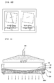
- FIG. 2A is a view illustrating the front surface of a polished wafer.
- the front surface of the wafer is measured using an LLS measurement apparatus, SP2, after polishing. And, as shown in FIG. 2A , ARC typed fine scratches are present on the front surface of the wafer. The scratches are caused by fine glass fibers and foreign materials from the edge of the wafer support member.
- FIG. 2B is a detailed view illustrating scratches present on the front surface of the wafer. As a result of detecting the front surface of the wafer using AFM, shallow scratches having a depth of 0.2 to 0.4 nm and a width of 300 to 600 nm were observed.
- the present invention is directed to a wafer support member, a method for manufacturing the same and a wafer pressing unit comprising the same that substantially obviate one or more problems due to limitations and disadvantages of the related art.
- a wafer support member including: a base substrate; a support adhered at a predetermined width to the edge of the base substrate, the support having a round outermost part; and a coating layer provided on the outermost edge of the support.
- a wafer polishing unit including: a wafer support member to support a wafer; a pressurizing unit to apply pressure to the wafer support member; and a pressure-supplying unit to supply pressure to the pressurizing unit, wherein the wafer support member includes a base substrate, a support adhered at a predetermined width to the edge of the base substrate, the support having a round outermost part and a coating layer provided on the outermost edge of the support.
- the coating layer may be an epoxy coating layer.
- the coating layer may be composed of a mixture of epoxy and a polymer at a weight ratio of 2:1 to 4:1.
- the coating layer may be provided to a thickness of 0.2 to 0.5 mm on the outermost edge of the round support.
- the coating layer may be wider than the round part of the support.
- a ratio of the width of the coating layer to the width of the round part of the support may be 1.4:1 to 1.6:1.
- a thickness deviation of the coating layer may be within ⁇ 0.1 mm.
- the coating layer may be further provided to a thickness of 0.1 to 0.3 mm in the non-round part of the support.
- a method for manufacturing a wafer support member including: laminating a support including a plurality of layers at the edge of a base substrate; rounding the edge of the support; and coating the round support.
- the coating may be carried out by applying a mixture of epoxy and a polymer at a ratio of 2:1 to 4:1, followed by drying.
- the coating may be carried out by applying a mixture of epoxy and a polymer at a thickness deviation within ⁇ 0.1 mm.
- the drying may be carried out by primarily drying the material at 45°C or higher and secondarily drying the material at ambient temperature.
- the coating may be carried out by applying a material containing epoxy and a polymer to a thickness of 0.2 to 0.5 mm to the round part of the edge of the support.
- the material may be applied to a 1.4- to 1.6-fold width of the width of the round part of the support.
- the material containing epoxy and a polymer may be applied to a thickness of 0.1 to 0.3 mm to the non-round part of the edge of the support.
- FIG. 1 is a view illustrating a conventional wafer support member
- FIGS. 2A to 2B are views illustrating the front surface of a polished wafer
- FIG. 3 is a view illustrating a wafer polishing unit according to one embodiment
- FIGS. 4A to 4D are views illustrating a method for manufacturing a wafer support member according to one embodiment.
- FIG. 5 is a view illustrating the width and thickness of the wafer support member according to one embodiment.
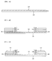
- FIG. 3 is a view illustrating a wafer polishing unit according to one embodiment.
- the wafer polishing unit includes a chamber 250, a pressure-supplying unit, a pressurizing unit, a wafer support member 200 and a fixing element 260, and may work as a pressing head.
- the pressurizing unit includes an expansion element 240 and the expansion element 240 may undergo variations in thickness and receive pressure and thus optionally expand.
- the chamber 250 forms a predetermined space with a back plate 270, an expansion element 240 and a fixing element 260.
- Pneumatic pressure is supplied from the pressure-supplying unit to the chamber 250 and the supplied pressure may vary the volume of the chamber 250.
- the pressure-supplying unit includes a pneumatic line 280 and a back plate 270.
- the back plate 270 has a round circular shape, which corresponds to the wafer.
- the pneumatic line 280 passes through the center of the back plate 270 and extends to the chamber 250, thus being capable of transferring the pneumatic pressure to the chamber 250.
- the pressurizing unit applies pneumatic pressure supplied to the chamber 250 to the wafer fixed in the wafer support member 200 and includes the expansion element 240.
- the expansion element 240 is made of a flexible material, which may be expanded by the pressure supplied through the pneumatic line 280 to the chamber 250.
- the expansion element 240 may be made of rubber and the edge thereof is fixed by the fixing element 260. Accordingly, the edge of the expansion element 240 may be thinner than the periphery thereof, since it is disadvantageously in view of expansion.
- the one surface of the wafer support member 200 contacts the expansion element 240 and the other surface thereof contacts the wafer.
- the wafer support member 200 receives pressure from the expansion element 240 and thus applies the pressure to the wafer.
- the fixing element 260 is arranged on the circumference of the back plate 270.
- the fixing element 260 fixes the edge of the expansion element 240. For this reason, the expansion element 260 can be secured to the wafer polishing unit, during expansion, and can maintain the pneumatic pressure in the chamber 250.
- FIGS. 4A to 4D are views illustrating a method for manufacturing a wafer support member according to one embodiment.
- the method for manufacturing a wafer support member according to one embodiment will be illustrated with referene to FIGS. 4A to 4D .
- a base substrate 220 is prepared.
- the base substrate 220 acts to support the wafer during the wafer polishing process.
- An adhesive agent 223 may be provided on the first surface of the base substrate 220 to adhere the wafer support member to the polishing unit in the following wafer polishing process.
- a double-sided adhesive agent may be used as the adhesive agent 230.
- the base substrate 220 is provided at one surface thereof with the adhesive agent 223 and at the other surface thereof with a wafer in the following process.
- the base substrate 220 may have the shape of a disc. For this reason, the base substrate 220 serves to support the disc-shaped wafer. The diameter of the base substrate 220 may be greater than that of the wafer.
- the support 210 is laminated on the edge of the base substrate 220.
- the support 210 may be composed of an epoxy glass.
- the support 210 is composed of a laminate including a plurality of layers 210a, 210b, 210c and 210d, thus obtaining a sufficient thickness.
- the support 210 is fixed on the base substrate 220 via an adhesive material 205.
- a hot melt sheet may be used as the adhesive material 205.
- the support 210 guides and supports the wafer such that the wafer is not separated from the head during the wafer polishing process. Accordingly, the support 210 may be adhered at a predetermined width to the periphery of the base substrate 220. An inner radius of the support 210 should be of a sufficient size to allow the wafer to be placed in the support 210.
- the edge of the support 210 is rounded. That is, as shown in the drawing, the edge of the top of the support 210 laminated on the base substrate 220 is smoothly rounded.
- edge refers to a part opposite to a region contacting the wafer.
- the peripheral top of the support 210 is primarily polished by a method using sand paper, etc. At this time, a part of the support 210 not to be processed may be protected using a mask (not shown).
- the remaining sand is removed through a process such as air cleaning.
- the part of the support 210 having been subjected to the primary polishing process, has a rough surface, thus requiring a smoothing process.
- the part polished in the afore-mentioned primary polishing process is secondarily polished by a method such as rubbing.
- the support is rounded through the primary polishing process and is smoothed through the secondary polishing process. Also, the residue present on the surface of the support after the secondary polishing process is thoroughly removed by cleaning with, for example, DIW.
- the rounded edge of the support 210 is coated. That is, the support 210 is coated to remove small amounts of impurities and etched materials left on the support 210 after primary and secondary polishing, air cleaning and DIW claning, make the polished rough part smooth and thus prevent damage to the polishing pad.
- a coating layer 215 may be coated on the outermost layer of the support 210.
- the coating material used herein may be epoxy.
- a predetermined ratio of epoxy as the coating material should be applied to the rounded part and be cured and dried under specific conditions.
- the coating layer 215 may not be cured to a desired level and may flow or foam, depending on the drying method.
- the coating material may be a mixture of epoxy and a polymer in a ratio of 10 to 3.
- the polymer used herein was a polymer (Toyo, Co., LTD.).
- the ratio of epoxy to polymer is preferably within a range of 2:1 to 4:1.
- the doped coating material is primarily dried at room temperature to 45°C or higher and is secondarily dried at room temperature.
- baking is mainly performed, the organic material present in the coating material is removed.
- the coating material is cured in the secondary drying process.
- the epoxy When the coating material is dried at an excessively low temperature, the epoxy is not sufficiently cured, and when the coating material is dried at an excessively high temperature, the adhesive material 205 may be detached.
- the coating layer 215 is formed on the periphery of the support 210 and the width and thickness thereof will be illustrated with reference to FIG. 5 .
- the edge of the uppermost layer of the support 210 is rounded through the polishing process.
- the coating layer 215 may be laminated to a thickness of 0.2 mm to 0.5 mm at the rouned edge of the support 210.
- the coating layer 215 When the thickness of the coating layer 215 is less than 0.2 mm, the coating layer 215 may be damaged in the wafer polishing process, and when the thickness of the coating layer 215 is 0.5 mm or higher, pressure is non-uniformly applied to the edge and the wafer may thus be separated from the wafer support member.
- the width (w 2 ) of the coating layer 215 may be greater than the width (w 1 ) of the rounded part of the support 210. That is, the coating layer 215 should be wider in order to protect the overall rounded part of the support 210.
- the width (W 1 ) of the rounded part of the support 210 is about 3.0 mm and may be processed within a deviation of 10%.
- a ratio between the width (W 1 ) of the rounded epoxy glass and the width (W 2 ) of the coating layer 215 may be about 1:1.4 to 1:1.6.
- the inner thickness of the coating layer 215 is greater than the outer thickness thereof. This is the reason that the epoxy applied before drying and curing may flow out.
- FIG. 4D A template assembly, as one wafer support member, manufactured in the afore-mentioned process, is shown in FIG. 4D .
- the base substrate 220 is provided at a first surface thereof with an adhesive agent 223 and at a second surface thereof with a support 210 through an adhesive material 205.
- the edge of the support 210 is rounded and is provided with a coating layer 215.
- the maximum thickness (T 1 ) of the coating layer 215 is about 0.5 mm and the coating layer 215 laminated on a non-rounded part of the support 210 may have a thickness (T 2 ) of about 0.1 mm to about 0.3 mm.
- the coated solution may flow sideways.
- the coating layer 215 thus obtained through the afore-mentioned process has a surface hardness of 82D or higher (based on a Brinell hardness tester). This surface hardness is required to allow the wafer support member to support the coating layer 215 until a wafer polishing process at 3,000 pcs is completed.
- the wafer surface may be mirror-polished by adhering a wafer to the wafer support member and applying pressure thereto in an expansion element 240. That is, pneumatic pressure is supplied from a pneumatic line 280 to the chamber 250, since the pneumatic line 280 passes through the back plate 270 and is connected to the chamber 250.
- the expansion element 240 When the inner pressure of the chamber 250 increases, the expansion element 240 is isolated from the back plate 270 and the expansion element 240 applies pressure to the wafer support member 200.
- the wafer support member 200 applies pressure to the wafer, the polishing process is performed while the wafer closely contacts a pad (not shown), and flatness of the wafer is improved through the polishing process.
- the support 210 provided on the edge of the wafer support member 200 is rounded and the coating layer 215 is provided on the edge. Accordingly, the support 210 guides and supports the wafer such that the wafer is not separated from the polishing head in the wafer polishing process, and foreign materials are removed through the rounding and epoxy coating and scratches in the wafer surface are thus reduced in size or eliminated.
- >37 nanometer PID defect percentage after a final polishing process can be decreased to about 2%. This value is lower than 25%, the defect percentate of conventional wafer support member not provided with an epoxy coating layer.
- a support provided on the edge of a wafer supporting portion is rounded and a coating layer is formed, thus preventing the wafer from being separated from a polishing head during polishing process and reducing scratches.
- the wafer support member may be applied to a carrier in a double side polishing process of wafer.
Landscapes
- Engineering & Computer Science (AREA)
- Mechanical Engineering (AREA)
- Finish Polishing, Edge Sharpening, And Grinding By Specific Grinding Devices (AREA)
- Mechanical Treatment Of Semiconductor (AREA)
Applications Claiming Priority (3)
| Application Number | Priority Date | Filing Date | Title |
|---|---|---|---|
| KR20090095195 | 2009-10-07 | ||
| KR1020100091172A KR101160266B1 (ko) | 2009-10-07 | 2010-09-16 | 웨이퍼 지지 부재, 그 제조방법 및 이를 포함하는 웨이퍼 연마 유닛 |
| PCT/KR2010/006755 WO2011043567A2 (ko) | 2009-10-07 | 2010-10-04 | 웨이퍼 지지 부재, 그 제조방법 및 이를 포함하는 웨이퍼 연마 유닛. |
Publications (2)
| Publication Number | Publication Date |
|---|---|
| EP2472571A2 true EP2472571A2 (de) | 2012-07-04 |
| EP2472571A4 EP2472571A4 (de) | 2015-07-01 |
Family
ID=44045251
Family Applications (1)
| Application Number | Title | Priority Date | Filing Date |
|---|---|---|---|
| EP10822212.6A Withdrawn EP2472571A4 (de) | 2009-10-07 | 2010-10-04 | Wafertrageelement, verfahren zu seiner herstellung und waferreinigungseinheit damit |
Country Status (5)
| Country | Link |
|---|---|
| US (1) | US8574033B2 (de) |
| EP (1) | EP2472571A4 (de) |
| JP (1) | JP2013507764A (de) |
| KR (1) | KR101160266B1 (de) |
| WO (1) | WO2011043567A2 (de) |
Families Citing this family (6)
| Publication number | Priority date | Publication date | Assignee | Title |
|---|---|---|---|---|
| JP7081915B2 (ja) * | 2017-10-16 | 2022-06-07 | 富士紡ホールディングス株式会社 | 研磨用保持具 |
| KR102485810B1 (ko) * | 2018-03-02 | 2023-01-09 | 주식회사 윌비에스엔티 | 화학적 기계적 연마 장치의 리테이너 링 |
| KR102270392B1 (ko) * | 2019-10-01 | 2021-06-30 | 에스케이실트론 주식회사 | 웨이퍼 연마 헤드, 웨이퍼 연마 헤드의 제조방법 및 그를 구비한 웨이퍼 연마 장치 |
| WO2021100978A1 (ko) * | 2019-11-20 | 2021-05-27 | 엘지디스플레이 주식회사 | 사이드 배선 제조 장치, 사이드 배선 제조 방법 및 표시 장치 제조 방법 |
| KR102304948B1 (ko) * | 2020-01-13 | 2021-09-24 | (주)제이쓰리 | 반도체 웨이퍼 형상을 제어하는 웨이퍼 가공용 헤드 장치 |
| CN115056045B (zh) * | 2022-06-30 | 2023-10-20 | 成都泰美克晶体技术有限公司 | 一种晶圆单面抛光装置及方法 |
Family Cites Families (29)
| Publication number | Priority date | Publication date | Assignee | Title |
|---|---|---|---|---|
| US6024630A (en) * | 1995-06-09 | 2000-02-15 | Applied Materials, Inc. | Fluid-pressure regulated wafer polishing head |
| JP3129172B2 (ja) * | 1995-11-14 | 2001-01-29 | 日本電気株式会社 | 研磨装置及び研磨方法 |
| KR0151102B1 (ko) * | 1996-02-28 | 1998-10-15 | 김광호 | 화학기계적 연마 장치 및 이를 이용한 화학기계적 연마방법 |
| US6019670A (en) * | 1997-03-10 | 2000-02-01 | Applied Materials, Inc. | Method and apparatus for conditioning a polishing pad in a chemical mechanical polishing system |
| JPH10286758A (ja) * | 1997-04-08 | 1998-10-27 | Ebara Corp | ポリッシング装置 |
| US6110025A (en) * | 1997-05-07 | 2000-08-29 | Obsidian, Inc. | Containment ring for substrate carrier apparatus |
| US5997392A (en) * | 1997-07-22 | 1999-12-07 | International Business Machines Corporation | Slurry injection technique for chemical-mechanical polishing |
| US6116992A (en) * | 1997-12-30 | 2000-09-12 | Applied Materials, Inc. | Substrate retaining ring |
| JP3966908B2 (ja) * | 1998-04-06 | 2007-08-29 | 株式会社荏原製作所 | ポリッシング装置 |
| JP2917992B1 (ja) * | 1998-04-10 | 1999-07-12 | 日本電気株式会社 | 研磨装置 |
| JP2000015572A (ja) * | 1998-04-29 | 2000-01-18 | Speedfam Co Ltd | キャリア及び研磨装置 |
| US6390904B1 (en) * | 1998-05-21 | 2002-05-21 | Applied Materials, Inc. | Retainers and non-abrasive liners used in chemical mechanical polishing |
| JP2000084836A (ja) * | 1998-09-08 | 2000-03-28 | Speedfam-Ipec Co Ltd | キャリア及び研磨装置 |
| TW436378B (en) * | 1999-02-05 | 2001-05-28 | Mitsubishi Materials Corp | Wafer polishing apparatus and method for making a wafer |
| US6368189B1 (en) * | 1999-03-03 | 2002-04-09 | Mitsubishi Materials Corporation | Apparatus and method for chemical-mechanical polishing (CMP) head having direct pneumatic wafer polishing pressure |
| KR100387385B1 (ko) * | 1999-03-03 | 2003-06-18 | 미츠비시 마테리알 가부시키가이샤 | 부상 웨이퍼 유지 링을 구비한 화학적 기계적 연마 헤드및 다중 구역 연마 압력 제어부를 갖춘 웨이퍼 캐리어 |
| US6354928B1 (en) * | 2000-04-21 | 2002-03-12 | Agere Systems Guardian Corp. | Polishing apparatus with carrier ring and carrier head employing like polarities |
| JP2002079461A (ja) * | 2000-09-07 | 2002-03-19 | Ebara Corp | ポリッシング装置 |
| US6719874B1 (en) * | 2001-03-30 | 2004-04-13 | Lam Research Corporation | Active retaining ring support |
| JP2003048155A (ja) * | 2001-08-03 | 2003-02-18 | Clariant (Japan) Kk | 化学的機械的研磨装置用ウェハー保持リング |
| CN1312740C (zh) * | 2001-09-28 | 2007-04-25 | 信越半导体株式会社 | 用于研磨的工件保持盘及工件研磨装置及研磨方法 |
| US6712673B2 (en) * | 2001-10-04 | 2004-03-30 | Memc Electronic Materials, Inc. | Polishing apparatus, polishing head and method |
| US6835125B1 (en) * | 2001-12-27 | 2004-12-28 | Applied Materials Inc. | Retainer with a wear surface for chemical mechanical polishing |
| JP2003236743A (ja) * | 2002-02-15 | 2003-08-26 | Rodel Nitta Co | 研磨用テンプレート |
| JP4159029B2 (ja) * | 2002-09-11 | 2008-10-01 | コバレントマテリアル株式会社 | セラミックス製プレート |
| US7344434B2 (en) * | 2003-11-13 | 2008-03-18 | Applied Materials, Inc. | Retaining ring with shaped surface |
| JP2007173815A (ja) * | 2005-12-20 | 2007-07-05 | Siltron Inc | シリコンウエハ研磨装置、これに使用されるリテーニングアセンブリ及びシリコンウエハ平坦度補正方法 |
| US8161909B2 (en) * | 2008-02-14 | 2012-04-24 | Julian Sprung | Magnetic cleaning device and methods of making and using such a cleaning device |
| KR100884236B1 (ko) * | 2008-05-27 | 2009-02-17 | (주)아이에스테크노 | 웨이퍼 연마용 리테이너 링 |
-
2010
- 2010-09-16 KR KR1020100091172A patent/KR101160266B1/ko active Active
- 2010-10-04 WO PCT/KR2010/006755 patent/WO2011043567A2/ko not_active Ceased
- 2010-10-04 EP EP10822212.6A patent/EP2472571A4/de not_active Withdrawn
- 2010-10-04 JP JP2012533073A patent/JP2013507764A/ja active Pending
- 2010-10-06 US US12/899,131 patent/US8574033B2/en active Active
Non-Patent Citations (1)
| Title |
|---|
| See references of WO2011043567A2 * |
Also Published As
| Publication number | Publication date |
|---|---|
| WO2011043567A3 (ko) | 2011-09-01 |
| WO2011043567A2 (ko) | 2011-04-14 |
| JP2013507764A (ja) | 2013-03-04 |
| EP2472571A4 (de) | 2015-07-01 |
| US20110081841A1 (en) | 2011-04-07 |
| KR20110037848A (ko) | 2011-04-13 |
| US8574033B2 (en) | 2013-11-05 |
| KR101160266B1 (ko) | 2012-06-27 |
Similar Documents
| Publication | Publication Date | Title |
|---|---|---|
| EP0737546B1 (de) | Haltevorrichtung für ein Substrat und Verfahren und Vorrichtung zum Polieren eines Substrates | |
| US8574033B2 (en) | Wafer support member, method for manufacturing the same and wafer polishing unit comprising the same | |
| US6764392B2 (en) | Wafer polishing method and wafer polishing device | |
| JPH09155730A (ja) | 研磨のための被加工物の保持具及びその製法 | |
| WO2008050475A1 (en) | Polishing head and polishing apparatus | |
| WO2011102078A1 (ja) | 研磨ヘッド及び研磨装置 | |
| JP4264289B2 (ja) | ウエーハ研磨装置及びその研磨ヘッド並びにウエーハ研磨方法 | |
| KR102466056B1 (ko) | 반도체 장치의 제조 방법 및 반도체 제조 장치 | |
| JP6252098B2 (ja) | 角形金型用基板 | |
| US11660724B2 (en) | Method for manufacturing a pad conditioner by reverse plating and pad conditioner manufactured thereby | |
| JP2020015142A (ja) | 研磨パッド | |
| WO2003038882A1 (en) | Method and pad for polishing wafer | |
| CN1986154A (zh) | 硅晶片研磨装置及其保持组件、硅晶片平整度校正方法 | |
| KR20100094466A (ko) | 연마 헤드 및 연마 장치 | |
| JP6239396B2 (ja) | Soi複合基板の製造方法 | |
| JP2004063880A (ja) | ウェーハ接着装置およびウェーハ接着方法 | |
| JP7386979B2 (ja) | ウエハー研磨ヘッド、ウエハー研磨ヘッドの製造方法及びそれを備えたウエハー研磨装置 | |
| JP2007266068A (ja) | 研磨方法及び研磨装置 | |
| JP2004241723A (ja) | 半導体ウエーハの製造方法、サポートリング及びサポートリング付ウエーハ | |
| JP3820432B2 (ja) | ウエーハ研磨方法 | |
| KR101596561B1 (ko) | 웨이퍼 연마 장치 | |
| WO2017125987A1 (ja) | ウェーハの研磨方法、バックパッドの製造方法、バックパッド、及びそのバックパッドを具備する研磨ヘッド | |
| JP4681970B2 (ja) | 研磨パッドおよび研磨機 | |
| JP3638138B2 (ja) | ウエーハ保持盤の作製方法及びウエーハの研磨方法 | |
| KR20110037662A (ko) | 템플레이트 어셈블리 및 그 제조방법 |
Legal Events
| Date | Code | Title | Description |
|---|---|---|---|
| PUAI | Public reference made under article 153(3) epc to a published international application that has entered the european phase |
Free format text: ORIGINAL CODE: 0009012 |
|
| 17P | Request for examination filed |
Effective date: 20120327 |
|
| AK | Designated contracting states |
Kind code of ref document: A2 Designated state(s): AL AT BE BG CH CY CZ DE DK EE ES FI FR GB GR HR HU IE IS IT LI LT LU LV MC MK MT NL NO PL PT RO RS SE SI SK SM TR |
|
| RIN1 | Information on inventor provided before grant (corrected) |
Inventor name: SUNG, JAE CHEL |
|
| R17D | Deferred search report published (corrected) |
Effective date: 20110901 |
|
| DAX | Request for extension of the european patent (deleted) | ||
| A4 | Supplementary search report drawn up and despatched |
Effective date: 20150601 |
|
| RIC1 | Information provided on ipc code assigned before grant |
Ipc: H01L 21/304 20060101AFI20150526BHEP Ipc: B24B 37/32 20120101ALI20150526BHEP |
|
| STAA | Information on the status of an ep patent application or granted ep patent |
Free format text: STATUS: THE APPLICATION IS DEEMED TO BE WITHDRAWN |
|
| 18D | Application deemed to be withdrawn |
Effective date: 20160105 |