EP2466587A2 - Semiconductor storage device - Google Patents
Semiconductor storage device Download PDFInfo
- Publication number
- EP2466587A2 EP2466587A2 EP11194028A EP11194028A EP2466587A2 EP 2466587 A2 EP2466587 A2 EP 2466587A2 EP 11194028 A EP11194028 A EP 11194028A EP 11194028 A EP11194028 A EP 11194028A EP 2466587 A2 EP2466587 A2 EP 2466587A2
- Authority
- EP
- European Patent Office
- Prior art keywords
- line
- transistor
- layer
- electrically connected
- input
- Prior art date
- Legal status (The legal status is an assumption and is not a legal conclusion. Google has not performed a legal analysis and makes no representation as to the accuracy of the status listed.)
- Granted
Links
- 239000004065 semiconductor Substances 0.000 title claims abstract description 359
- 238000003860 storage Methods 0.000 title claims abstract description 63
- 239000011159 matrix material Substances 0.000 claims abstract description 7
- 239000003990 capacitor Substances 0.000 claims description 30
- 239000010410 layer Substances 0.000 description 663
- 239000000463 material Substances 0.000 description 69
- 238000010438 heat treatment Methods 0.000 description 61
- 239000000758 substrate Substances 0.000 description 51
- 238000000034 method Methods 0.000 description 49
- 229910007541 Zn O Inorganic materials 0.000 description 42
- 238000005530 etching Methods 0.000 description 40
- 239000011229 interlayer Substances 0.000 description 39
- 239000012535 impurity Substances 0.000 description 37
- 239000007789 gas Substances 0.000 description 32
- 239000012298 atmosphere Substances 0.000 description 30
- 238000005259 measurement Methods 0.000 description 30
- 239000011701 zinc Substances 0.000 description 30
- 239000001257 hydrogen Substances 0.000 description 29
- 229910052739 hydrogen Inorganic materials 0.000 description 29
- XKRFYHLGVUSROY-UHFFFAOYSA-N Argon Chemical compound [Ar] XKRFYHLGVUSROY-UHFFFAOYSA-N 0.000 description 28
- QVGXLLKOCUKJST-UHFFFAOYSA-N atomic oxygen Chemical compound [O] QVGXLLKOCUKJST-UHFFFAOYSA-N 0.000 description 27
- 239000001301 oxygen Substances 0.000 description 27
- 229910052760 oxygen Inorganic materials 0.000 description 27
- 230000001681 protective effect Effects 0.000 description 27
- RTAQQCXQSZGOHL-UHFFFAOYSA-N Titanium Chemical compound [Ti] RTAQQCXQSZGOHL-UHFFFAOYSA-N 0.000 description 26
- 230000015572 biosynthetic process Effects 0.000 description 26
- 229910052719 titanium Inorganic materials 0.000 description 26
- 239000010936 titanium Substances 0.000 description 26
- UFHFLCQGNIYNRP-UHFFFAOYSA-N Hydrogen Chemical compound [H][H] UFHFLCQGNIYNRP-UHFFFAOYSA-N 0.000 description 25
- 238000004544 sputter deposition Methods 0.000 description 25
- 230000002829 reductive effect Effects 0.000 description 22
- IJGRMHOSHXDMSA-UHFFFAOYSA-N Atomic nitrogen Chemical compound N#N IJGRMHOSHXDMSA-UHFFFAOYSA-N 0.000 description 18
- 229910052581 Si3N4 Inorganic materials 0.000 description 18
- HQVNEWCFYHHQES-UHFFFAOYSA-N silicon nitride Chemical compound N12[Si]34N5[Si]62N3[Si]51N64 HQVNEWCFYHHQES-UHFFFAOYSA-N 0.000 description 18
- 229910052751 metal Inorganic materials 0.000 description 17
- XUIMIQQOPSSXEZ-UHFFFAOYSA-N Silicon Chemical compound [Si] XUIMIQQOPSSXEZ-UHFFFAOYSA-N 0.000 description 16
- 230000008569 process Effects 0.000 description 16
- 229910052710 silicon Inorganic materials 0.000 description 16
- 239000010703 silicon Substances 0.000 description 16
- VYPSYNLAJGMNEJ-UHFFFAOYSA-N Silicium dioxide Chemical compound O=[Si]=O VYPSYNLAJGMNEJ-UHFFFAOYSA-N 0.000 description 15
- 229910052782 aluminium Inorganic materials 0.000 description 15
- 229910052786 argon Inorganic materials 0.000 description 15
- XLOMVQKBTHCTTD-UHFFFAOYSA-N Zinc monoxide Chemical compound [Zn]=O XLOMVQKBTHCTTD-UHFFFAOYSA-N 0.000 description 14
- 239000004020 conductor Substances 0.000 description 14
- 150000002736 metal compounds Chemical group 0.000 description 14
- XAGFODPZIPBFFR-UHFFFAOYSA-N aluminium Chemical compound [Al] XAGFODPZIPBFFR-UHFFFAOYSA-N 0.000 description 13
- 229910044991 metal oxide Inorganic materials 0.000 description 13
- 150000004706 metal oxides Chemical class 0.000 description 13
- WFKWXMTUELFFGS-UHFFFAOYSA-N tungsten Chemical compound [W] WFKWXMTUELFFGS-UHFFFAOYSA-N 0.000 description 13
- 229910052721 tungsten Inorganic materials 0.000 description 13
- 239000010937 tungsten Substances 0.000 description 13
- 239000013078 crystal Substances 0.000 description 11
- 238000010586 diagram Methods 0.000 description 11
- 238000007667 floating Methods 0.000 description 11
- 238000000206 photolithography Methods 0.000 description 11
- 238000012545 processing Methods 0.000 description 11
- 229910052814 silicon oxide Inorganic materials 0.000 description 11
- 238000009825 accumulation Methods 0.000 description 10
- 238000001312 dry etching Methods 0.000 description 10
- 239000002184 metal Substances 0.000 description 10
- 238000005240 physical vapour deposition Methods 0.000 description 10
- XLYOFNOQVPJJNP-UHFFFAOYSA-N water Substances O XLYOFNOQVPJJNP-UHFFFAOYSA-N 0.000 description 10
- 238000000151 deposition Methods 0.000 description 9
- 230000008021 deposition Effects 0.000 description 9
- 229910052733 gallium Inorganic materials 0.000 description 9
- 239000000203 mixture Substances 0.000 description 9
- 229910052757 nitrogen Inorganic materials 0.000 description 9
- 239000012299 nitrogen atmosphere Substances 0.000 description 9
- 239000011787 zinc oxide Substances 0.000 description 9
- RYGMFSIKBFXOCR-UHFFFAOYSA-N Copper Chemical compound [Cu] RYGMFSIKBFXOCR-UHFFFAOYSA-N 0.000 description 8
- NRTOMJZYCJJWKI-UHFFFAOYSA-N Titanium nitride Chemical compound [Ti]#N NRTOMJZYCJJWKI-UHFFFAOYSA-N 0.000 description 8
- 229910052802 copper Inorganic materials 0.000 description 8
- 239000010949 copper Substances 0.000 description 8
- 230000006870 function Effects 0.000 description 8
- 230000007257 malfunction Effects 0.000 description 8
- 229910052738 indium Inorganic materials 0.000 description 7
- 230000014759 maintenance of location Effects 0.000 description 7
- 229910052715 tantalum Inorganic materials 0.000 description 7
- GUVRBAGPIYLISA-UHFFFAOYSA-N tantalum atom Chemical compound [Ta] GUVRBAGPIYLISA-UHFFFAOYSA-N 0.000 description 7
- 238000001039 wet etching Methods 0.000 description 7
- 229910052725 zinc Inorganic materials 0.000 description 7
- 229910019092 Mg-O Inorganic materials 0.000 description 6
- 229910019395 Mg—O Inorganic materials 0.000 description 6
- 125000004429 atom Chemical group 0.000 description 6
- 150000001875 compounds Chemical class 0.000 description 6
- TWNQGVIAIRXVLR-UHFFFAOYSA-N oxo(oxoalumanyloxy)alumane Chemical compound O=[Al]O[Al]=O TWNQGVIAIRXVLR-UHFFFAOYSA-N 0.000 description 6
- VYZAMTAEIAYCRO-UHFFFAOYSA-N Chromium Chemical compound [Cr] VYZAMTAEIAYCRO-UHFFFAOYSA-N 0.000 description 5
- ZOKXTWBITQBERF-UHFFFAOYSA-N Molybdenum Chemical compound [Mo] ZOKXTWBITQBERF-UHFFFAOYSA-N 0.000 description 5
- 229910045601 alloy Inorganic materials 0.000 description 5
- 239000000956 alloy Substances 0.000 description 5
- 230000008859 change Effects 0.000 description 5
- 229910052804 chromium Inorganic materials 0.000 description 5
- 239000011651 chromium Substances 0.000 description 5
- 229910000449 hafnium oxide Inorganic materials 0.000 description 5
- WIHZLLGSGQNAGK-UHFFFAOYSA-N hafnium(4+);oxygen(2-) Chemical compound [O-2].[O-2].[Hf+4] WIHZLLGSGQNAGK-UHFFFAOYSA-N 0.000 description 5
- 229910052734 helium Inorganic materials 0.000 description 5
- 238000004519 manufacturing process Methods 0.000 description 5
- 239000007769 metal material Substances 0.000 description 5
- 229910052750 molybdenum Inorganic materials 0.000 description 5
- 239000011733 molybdenum Substances 0.000 description 5
- BPUBBGLMJRNUCC-UHFFFAOYSA-N oxygen(2-);tantalum(5+) Chemical compound [O-2].[O-2].[O-2].[O-2].[O-2].[Ta+5].[Ta+5] BPUBBGLMJRNUCC-UHFFFAOYSA-N 0.000 description 5
- 238000009832 plasma treatment Methods 0.000 description 5
- 238000000623 plasma-assisted chemical vapour deposition Methods 0.000 description 5
- 239000011241 protective layer Substances 0.000 description 5
- 230000000717 retained effect Effects 0.000 description 5
- 238000001004 secondary ion mass spectrometry Methods 0.000 description 5
- 239000002356 single layer Substances 0.000 description 5
- 229910001936 tantalum oxide Inorganic materials 0.000 description 5
- 229910052779 Neodymium Inorganic materials 0.000 description 4
- 239000012300 argon atmosphere Substances 0.000 description 4
- 230000004888 barrier function Effects 0.000 description 4
- 230000008901 benefit Effects 0.000 description 4
- QZQVBEXLDFYHSR-UHFFFAOYSA-N gallium(III) oxide Inorganic materials O=[Ga]O[Ga]=O QZQVBEXLDFYHSR-UHFFFAOYSA-N 0.000 description 4
- 239000001307 helium Substances 0.000 description 4
- SWQJXJOGLNCZEY-UHFFFAOYSA-N helium atom Chemical compound [He] SWQJXJOGLNCZEY-UHFFFAOYSA-N 0.000 description 4
- 150000002431 hydrogen Chemical class 0.000 description 4
- 125000004435 hydrogen atom Chemical group [H]* 0.000 description 4
- PJXISJQVUVHSOJ-UHFFFAOYSA-N indium(III) oxide Inorganic materials [O-2].[O-2].[O-2].[In+3].[In+3] PJXISJQVUVHSOJ-UHFFFAOYSA-N 0.000 description 4
- 239000011261 inert gas Substances 0.000 description 4
- 239000011810 insulating material Substances 0.000 description 4
- 238000002955 isolation Methods 0.000 description 4
- 239000011777 magnesium Substances 0.000 description 4
- QEFYFXOXNSNQGX-UHFFFAOYSA-N neodymium atom Chemical compound [Nd] QEFYFXOXNSNQGX-UHFFFAOYSA-N 0.000 description 4
- 238000004151 rapid thermal annealing Methods 0.000 description 4
- 229910052706 scandium Inorganic materials 0.000 description 4
- SIXSYDAISGFNSX-UHFFFAOYSA-N scandium atom Chemical compound [Sc] SIXSYDAISGFNSX-UHFFFAOYSA-N 0.000 description 4
- VZGDMQKNWNREIO-UHFFFAOYSA-N tetrachloromethane Chemical compound ClC(Cl)(Cl)Cl VZGDMQKNWNREIO-UHFFFAOYSA-N 0.000 description 4
- QTBSBXVTEAMEQO-UHFFFAOYSA-N Acetic acid Chemical compound CC(O)=O QTBSBXVTEAMEQO-UHFFFAOYSA-N 0.000 description 3
- ZOXJGFHDIHLPTG-UHFFFAOYSA-N Boron Chemical compound [B] ZOXJGFHDIHLPTG-UHFFFAOYSA-N 0.000 description 3
- ZAMOUSCENKQFHK-UHFFFAOYSA-N Chlorine atom Chemical compound [Cl] ZAMOUSCENKQFHK-UHFFFAOYSA-N 0.000 description 3
- 208000005156 Dehydration Diseases 0.000 description 3
- XPDWGBQVDMORPB-UHFFFAOYSA-N Fluoroform Chemical compound FC(F)F XPDWGBQVDMORPB-UHFFFAOYSA-N 0.000 description 3
- GYHNNYVSQQEPJS-UHFFFAOYSA-N Gallium Chemical compound [Ga] GYHNNYVSQQEPJS-UHFFFAOYSA-N 0.000 description 3
- 101000648528 Homo sapiens Transmembrane protein 50A Proteins 0.000 description 3
- PXHVJJICTQNCMI-UHFFFAOYSA-N Nickel Chemical compound [Ni] PXHVJJICTQNCMI-UHFFFAOYSA-N 0.000 description 3
- MWUXSHHQAYIFBG-UHFFFAOYSA-N Nitric oxide Chemical compound O=[N] MWUXSHHQAYIFBG-UHFFFAOYSA-N 0.000 description 3
- OAICVXFJPJFONN-UHFFFAOYSA-N Phosphorus Chemical compound [P] OAICVXFJPJFONN-UHFFFAOYSA-N 0.000 description 3
- 102100028770 Transmembrane protein 50A Human genes 0.000 description 3
- HCHKCACWOHOZIP-UHFFFAOYSA-N Zinc Chemical compound [Zn] HCHKCACWOHOZIP-UHFFFAOYSA-N 0.000 description 3
- NIXOWILDQLNWCW-UHFFFAOYSA-N acrylic acid group Chemical group C(C=C)(=O)O NIXOWILDQLNWCW-UHFFFAOYSA-N 0.000 description 3
- 229910052785 arsenic Inorganic materials 0.000 description 3
- RQNWIZPPADIBDY-UHFFFAOYSA-N arsenic atom Chemical compound [As] RQNWIZPPADIBDY-UHFFFAOYSA-N 0.000 description 3
- 229910052796 boron Inorganic materials 0.000 description 3
- 229910052799 carbon Inorganic materials 0.000 description 3
- 239000000460 chlorine Substances 0.000 description 3
- 229910052801 chlorine Inorganic materials 0.000 description 3
- 238000002425 crystallisation Methods 0.000 description 3
- 230000008025 crystallization Effects 0.000 description 3
- 230000003247 decreasing effect Effects 0.000 description 3
- 230000018044 dehydration Effects 0.000 description 3
- 238000006297 dehydration reaction Methods 0.000 description 3
- 238000006356 dehydrogenation reaction Methods 0.000 description 3
- 239000000284 extract Substances 0.000 description 3
- 230000002349 favourable effect Effects 0.000 description 3
- 239000011521 glass Substances 0.000 description 3
- 125000002887 hydroxy group Chemical group [H]O* 0.000 description 3
- 150000002500 ions Chemical class 0.000 description 3
- 229910052749 magnesium Inorganic materials 0.000 description 3
- 229910052698 phosphorus Inorganic materials 0.000 description 3
- 239000011574 phosphorus Substances 0.000 description 3
- 230000009291 secondary effect Effects 0.000 description 3
- VXEGSRKPIUDPQT-UHFFFAOYSA-N 4-[4-(4-methoxyphenyl)piperazin-1-yl]aniline Chemical compound C1=CC(OC)=CC=C1N1CCN(C=2C=CC(N)=CC=2)CC1 VXEGSRKPIUDPQT-UHFFFAOYSA-N 0.000 description 2
- 229910018137 Al-Zn Inorganic materials 0.000 description 2
- 229910018573 Al—Zn Inorganic materials 0.000 description 2
- QGZKDVFQNNGYKY-UHFFFAOYSA-N Ammonia Chemical compound N QGZKDVFQNNGYKY-UHFFFAOYSA-N 0.000 description 2
- YCKRFDGAMUMZLT-UHFFFAOYSA-N Fluorine atom Chemical compound [F] YCKRFDGAMUMZLT-UHFFFAOYSA-N 0.000 description 2
- 108010083687 Ion Pumps Proteins 0.000 description 2
- WHXSMMKQMYFTQS-UHFFFAOYSA-N Lithium Chemical compound [Li] WHXSMMKQMYFTQS-UHFFFAOYSA-N 0.000 description 2
- FYYHWMGAXLPEAU-UHFFFAOYSA-N Magnesium Chemical compound [Mg] FYYHWMGAXLPEAU-UHFFFAOYSA-N 0.000 description 2
- NBIIXXVUZAFLBC-UHFFFAOYSA-N Phosphoric acid Chemical compound OP(O)(O)=O NBIIXXVUZAFLBC-UHFFFAOYSA-N 0.000 description 2
- 229910018503 SF6 Inorganic materials 0.000 description 2
- BLRPTPMANUNPDV-UHFFFAOYSA-N Silane Chemical compound [SiH4] BLRPTPMANUNPDV-UHFFFAOYSA-N 0.000 description 2
- 229910020868 Sn-Ga-Zn Inorganic materials 0.000 description 2
- 229910020923 Sn-O Inorganic materials 0.000 description 2
- 229910020994 Sn-Zn Inorganic materials 0.000 description 2
- 229910009069 Sn—Zn Inorganic materials 0.000 description 2
- 101100129180 Streptococcus pyogenes serotype M5 emm5 gene Proteins 0.000 description 2
- 230000002411 adverse Effects 0.000 description 2
- 238000004458 analytical method Methods 0.000 description 2
- 230000015556 catabolic process Effects 0.000 description 2
- 238000006243 chemical reaction Methods 0.000 description 2
- 229910052681 coesite Inorganic materials 0.000 description 2
- 238000004891 communication Methods 0.000 description 2
- 230000008878 coupling Effects 0.000 description 2
- 238000010168 coupling process Methods 0.000 description 2
- 238000005859 coupling reaction Methods 0.000 description 2
- 229910052906 cristobalite Inorganic materials 0.000 description 2
- 238000006731 degradation reaction Methods 0.000 description 2
- 230000006866 deterioration Effects 0.000 description 2
- 238000009792 diffusion process Methods 0.000 description 2
- AJNVQOSZGJRYEI-UHFFFAOYSA-N digallium;oxygen(2-) Chemical compound [O-2].[O-2].[O-2].[Ga+3].[Ga+3] AJNVQOSZGJRYEI-UHFFFAOYSA-N 0.000 description 2
- 239000000428 dust Substances 0.000 description 2
- 238000011049 filling Methods 0.000 description 2
- 229910052731 fluorine Inorganic materials 0.000 description 2
- 239000011737 fluorine Substances 0.000 description 2
- 235000013305 food Nutrition 0.000 description 2
- 229910001195 gallium oxide Inorganic materials 0.000 description 2
- 150000004678 hydrides Chemical class 0.000 description 2
- APFVFJFRJDLVQX-UHFFFAOYSA-N indium atom Chemical compound [In] APFVFJFRJDLVQX-UHFFFAOYSA-N 0.000 description 2
- 238000009616 inductively coupled plasma Methods 0.000 description 2
- 229910052744 lithium Inorganic materials 0.000 description 2
- 239000013081 microcrystal Substances 0.000 description 2
- QKCGXXHCELUCKW-UHFFFAOYSA-N n-[4-[4-(dinaphthalen-2-ylamino)phenyl]phenyl]-n-naphthalen-2-ylnaphthalen-2-amine Chemical compound C1=CC=CC2=CC(N(C=3C=CC(=CC=3)C=3C=CC(=CC=3)N(C=3C=C4C=CC=CC4=CC=3)C=3C=C4C=CC=CC4=CC=3)C3=CC4=CC=CC=C4C=C3)=CC=C21 QKCGXXHCELUCKW-UHFFFAOYSA-N 0.000 description 2
- 229910052754 neon Inorganic materials 0.000 description 2
- GKAOGPIIYCISHV-UHFFFAOYSA-N neon atom Chemical compound [Ne] GKAOGPIIYCISHV-UHFFFAOYSA-N 0.000 description 2
- 229910052759 nickel Inorganic materials 0.000 description 2
- 150000004767 nitrides Chemical class 0.000 description 2
- 238000004806 packaging method and process Methods 0.000 description 2
- 230000003071 parasitic effect Effects 0.000 description 2
- 238000000059 patterning Methods 0.000 description 2
- 238000001020 plasma etching Methods 0.000 description 2
- 238000007747 plating Methods 0.000 description 2
- BASFCYQUMIYNBI-UHFFFAOYSA-N platinum Chemical compound [Pt] BASFCYQUMIYNBI-UHFFFAOYSA-N 0.000 description 2
- 238000005498 polishing Methods 0.000 description 2
- 229910021420 polycrystalline silicon Inorganic materials 0.000 description 2
- 230000005855 radiation Effects 0.000 description 2
- 230000009467 reduction Effects 0.000 description 2
- 230000002441 reversible effect Effects 0.000 description 2
- 239000000377 silicon dioxide Substances 0.000 description 2
- 239000005049 silicon tetrachloride Substances 0.000 description 2
- 238000004528 spin coating Methods 0.000 description 2
- 238000005477 sputtering target Methods 0.000 description 2
- 229910052682 stishovite Inorganic materials 0.000 description 2
- 238000000859 sublimation Methods 0.000 description 2
- 230000008022 sublimation Effects 0.000 description 2
- 239000000126 substance Substances 0.000 description 2
- JBQYATWDVHIOAR-UHFFFAOYSA-N tellanylidenegermanium Chemical compound [Te]=[Ge] JBQYATWDVHIOAR-UHFFFAOYSA-N 0.000 description 2
- TXEYQDLBPFQVAA-UHFFFAOYSA-N tetrafluoromethane Chemical compound FC(F)(F)F TXEYQDLBPFQVAA-UHFFFAOYSA-N 0.000 description 2
- 229910052718 tin Inorganic materials 0.000 description 2
- FAQYAMRNWDIXMY-UHFFFAOYSA-N trichloroborane Chemical compound ClB(Cl)Cl FAQYAMRNWDIXMY-UHFFFAOYSA-N 0.000 description 2
- 229910052905 tridymite Inorganic materials 0.000 description 2
- 238000007738 vacuum evaporation Methods 0.000 description 2
- ZSLUVFAKFWKJRC-IGMARMGPSA-N 232Th Chemical compound [232Th] ZSLUVFAKFWKJRC-IGMARMGPSA-N 0.000 description 1
- 229910018120 Al-Ga-Zn Inorganic materials 0.000 description 1
- OKTJSMMVPCPJKN-UHFFFAOYSA-N Carbon Chemical compound [C] OKTJSMMVPCPJKN-UHFFFAOYSA-N 0.000 description 1
- KZBUYRJDOAKODT-UHFFFAOYSA-N Chlorine Chemical compound ClCl KZBUYRJDOAKODT-UHFFFAOYSA-N 0.000 description 1
- MYMOFIZGZYHOMD-UHFFFAOYSA-N Dioxygen Chemical compound O=O MYMOFIZGZYHOMD-UHFFFAOYSA-N 0.000 description 1
- 102100036250 GPI mannosyltransferase 4 Human genes 0.000 description 1
- 230000005355 Hall effect Effects 0.000 description 1
- 101001074618 Homo sapiens GPI mannosyltransferase 4 Proteins 0.000 description 1
- 101000983850 Homo sapiens Phosphatidate phosphatase LPIN3 Proteins 0.000 description 1
- CPELXLSAUQHCOX-UHFFFAOYSA-N Hydrogen bromide Chemical compound Br CPELXLSAUQHCOX-UHFFFAOYSA-N 0.000 description 1
- DGAQECJNVWCQMB-PUAWFVPOSA-M Ilexoside XXIX Chemical compound C[C@@H]1CC[C@@]2(CC[C@@]3(C(=CC[C@H]4[C@]3(CC[C@@H]5[C@@]4(CC[C@@H](C5(C)C)OS(=O)(=O)[O-])C)C)[C@@H]2[C@]1(C)O)C)C(=O)O[C@H]6[C@@H]([C@H]([C@@H]([C@H](O6)CO)O)O)O.[Na+] DGAQECJNVWCQMB-PUAWFVPOSA-M 0.000 description 1
- HBBGRARXTFLTSG-UHFFFAOYSA-N Lithium ion Chemical compound [Li+] HBBGRARXTFLTSG-UHFFFAOYSA-N 0.000 description 1
- 241001465754 Metazoa Species 0.000 description 1
- GRYLNZFGIOXLOG-UHFFFAOYSA-N Nitric acid Chemical compound O[N+]([O-])=O GRYLNZFGIOXLOG-UHFFFAOYSA-N 0.000 description 1
- GQPLMRYTRLFLPF-UHFFFAOYSA-N Nitrous Oxide Chemical compound [O-][N+]#N GQPLMRYTRLFLPF-UHFFFAOYSA-N 0.000 description 1
- 102100025728 Phosphatidate phosphatase LPIN3 Human genes 0.000 description 1
- 239000004642 Polyimide Substances 0.000 description 1
- 241000206607 Porphyra umbilicalis Species 0.000 description 1
- 229910000577 Silicon-germanium Inorganic materials 0.000 description 1
- 229910020833 Sn-Al-Zn Inorganic materials 0.000 description 1
- 229910020944 Sn-Mg Inorganic materials 0.000 description 1
- 229910052776 Thorium Inorganic materials 0.000 description 1
- ATJFFYVFTNAWJD-UHFFFAOYSA-N Tin Chemical compound [Sn] ATJFFYVFTNAWJD-UHFFFAOYSA-N 0.000 description 1
- 229910000611 Zinc aluminium Inorganic materials 0.000 description 1
- QCWXUUIWCKQGHC-UHFFFAOYSA-N Zirconium Chemical compound [Zr] QCWXUUIWCKQGHC-UHFFFAOYSA-N 0.000 description 1
- 229910009369 Zn Mg Inorganic materials 0.000 description 1
- 229910007573 Zn-Mg Inorganic materials 0.000 description 1
- LEVVHYCKPQWKOP-UHFFFAOYSA-N [Si].[Ge] Chemical compound [Si].[Ge] LEVVHYCKPQWKOP-UHFFFAOYSA-N 0.000 description 1
- HXFVOUUOTHJFPX-UHFFFAOYSA-N alumane;zinc Chemical compound [AlH3].[Zn] HXFVOUUOTHJFPX-UHFFFAOYSA-N 0.000 description 1
- 229910000147 aluminium phosphate Inorganic materials 0.000 description 1
- JYMITAMFTJDTAE-UHFFFAOYSA-N aluminum zinc oxygen(2-) Chemical compound [O-2].[Al+3].[Zn+2] JYMITAMFTJDTAE-UHFFFAOYSA-N 0.000 description 1
- 229910021529 ammonia Inorganic materials 0.000 description 1
- 238000004380 ashing Methods 0.000 description 1
- 229910052790 beryllium Inorganic materials 0.000 description 1
- ATBAMAFKBVZNFJ-UHFFFAOYSA-N beryllium atom Chemical compound [Be] ATBAMAFKBVZNFJ-UHFFFAOYSA-N 0.000 description 1
- OJIJEKBXJYRIBZ-UHFFFAOYSA-N cadmium nickel Chemical compound [Ni].[Cd] OJIJEKBXJYRIBZ-UHFFFAOYSA-N 0.000 description 1
- 150000001721 carbon Chemical group 0.000 description 1
- 229910017052 cobalt Inorganic materials 0.000 description 1
- 239000010941 cobalt Substances 0.000 description 1
- GUTLYIVDDKVIGB-UHFFFAOYSA-N cobalt atom Chemical compound [Co] GUTLYIVDDKVIGB-UHFFFAOYSA-N 0.000 description 1
- 230000007423 decrease Effects 0.000 description 1
- 230000007547 defect Effects 0.000 description 1
- 238000013461 design Methods 0.000 description 1
- 229910001882 dioxygen Inorganic materials 0.000 description 1
- 238000009826 distribution Methods 0.000 description 1
- 230000000694 effects Effects 0.000 description 1
- 238000010891 electric arc Methods 0.000 description 1
- 238000005566 electron beam evaporation Methods 0.000 description 1
- WRQGPGZATPOHHX-UHFFFAOYSA-N ethyl 2-oxohexanoate Chemical compound CCCCC(=O)C(=O)OCC WRQGPGZATPOHHX-UHFFFAOYSA-N 0.000 description 1
- 238000001704 evaporation Methods 0.000 description 1
- 230000008020 evaporation Effects 0.000 description 1
- 230000005669 field effect Effects 0.000 description 1
- 239000011245 gel electrolyte Substances 0.000 description 1
- 229910052735 hafnium Inorganic materials 0.000 description 1
- 229910052736 halogen Inorganic materials 0.000 description 1
- 150000002367 halogens Chemical class 0.000 description 1
- AMGQUBHHOARCQH-UHFFFAOYSA-N indium;oxotin Chemical compound [In].[Sn]=O AMGQUBHHOARCQH-UHFFFAOYSA-N 0.000 description 1
- 238000002347 injection Methods 0.000 description 1
- 239000007924 injection Substances 0.000 description 1
- 238000007641 inkjet printing Methods 0.000 description 1
- 238000007689 inspection Methods 0.000 description 1
- 238000007733 ion plating Methods 0.000 description 1
- 229910052743 krypton Inorganic materials 0.000 description 1
- 229910052747 lanthanoid Inorganic materials 0.000 description 1
- 150000002602 lanthanoids Chemical class 0.000 description 1
- 239000004973 liquid crystal related substance Substances 0.000 description 1
- 229910001416 lithium ion Inorganic materials 0.000 description 1
- 239000000696 magnetic material Substances 0.000 description 1
- 229910052748 manganese Inorganic materials 0.000 description 1
- 239000011572 manganese Substances 0.000 description 1
- WPBNNNQJVZRUHP-UHFFFAOYSA-L manganese(2+);methyl n-[[2-(methoxycarbonylcarbamothioylamino)phenyl]carbamothioyl]carbamate;n-[2-(sulfidocarbothioylamino)ethyl]carbamodithioate Chemical compound [Mn+2].[S-]C(=S)NCCNC([S-])=S.COC(=O)NC(=S)NC1=CC=CC=C1NC(=S)NC(=O)OC WPBNNNQJVZRUHP-UHFFFAOYSA-L 0.000 description 1
- 238000000691 measurement method Methods 0.000 description 1
- QSHDDOUJBYECFT-UHFFFAOYSA-N mercury Chemical compound [Hg] QSHDDOUJBYECFT-UHFFFAOYSA-N 0.000 description 1
- 229910052753 mercury Inorganic materials 0.000 description 1
- 229910001507 metal halide Inorganic materials 0.000 description 1
- 150000005309 metal halides Chemical class 0.000 description 1
- 229910052987 metal hydride Inorganic materials 0.000 description 1
- 239000011259 mixed solution Substances 0.000 description 1
- 230000004048 modification Effects 0.000 description 1
- 238000012986 modification Methods 0.000 description 1
- 229910021421 monocrystalline silicon Inorganic materials 0.000 description 1
- -1 nickel metal hydride Chemical class 0.000 description 1
- 229910017604 nitric acid Inorganic materials 0.000 description 1
- 230000003287 optical effect Effects 0.000 description 1
- 230000010355 oscillation Effects 0.000 description 1
- 230000003647 oxidation Effects 0.000 description 1
- 238000007254 oxidation reaction Methods 0.000 description 1
- 230000036961 partial effect Effects 0.000 description 1
- 230000002093 peripheral effect Effects 0.000 description 1
- 229910052697 platinum Inorganic materials 0.000 description 1
- 229920001721 polyimide Polymers 0.000 description 1
- 229920000642 polymer Polymers 0.000 description 1
- 239000002243 precursor Substances 0.000 description 1
- 239000011347 resin Substances 0.000 description 1
- 229920005989 resin Polymers 0.000 description 1
- 229910000077 silane Inorganic materials 0.000 description 1
- HBMJWWWQQXIZIP-UHFFFAOYSA-N silicon carbide Chemical compound [Si+]#[C-] HBMJWWWQQXIZIP-UHFFFAOYSA-N 0.000 description 1
- 229910010271 silicon carbide Inorganic materials 0.000 description 1
- 239000011734 sodium Substances 0.000 description 1
- 229910052708 sodium Inorganic materials 0.000 description 1
- 238000001228 spectrum Methods 0.000 description 1
- 238000005507 spraying Methods 0.000 description 1
- 230000003068 static effect Effects 0.000 description 1
- KXRZBTAEDBELFD-UHFFFAOYSA-N sulfamethopyrazine Chemical compound COC1=NC=CN=C1NS(=O)(=O)C1=CC=C(N)C=C1 KXRZBTAEDBELFD-UHFFFAOYSA-N 0.000 description 1
- SFZCNBIFKDRMGX-UHFFFAOYSA-N sulfur hexafluoride Chemical compound FS(F)(F)(F)(F)F SFZCNBIFKDRMGX-UHFFFAOYSA-N 0.000 description 1
- 229960000909 sulfur hexafluoride Drugs 0.000 description 1
- 238000012546 transfer Methods 0.000 description 1
- 230000001052 transient effect Effects 0.000 description 1
- 230000005641 tunneling Effects 0.000 description 1
- 229910052724 xenon Inorganic materials 0.000 description 1
- FHNFHKCVQCLJFQ-UHFFFAOYSA-N xenon atom Chemical compound [Xe] FHNFHKCVQCLJFQ-UHFFFAOYSA-N 0.000 description 1
- 229910052726 zirconium Inorganic materials 0.000 description 1
Images









Classifications
-
- G—PHYSICS
- G11—INFORMATION STORAGE
- G11C—STATIC STORES
- G11C7/00—Arrangements for writing information into, or reading information out from, a digital store
- G11C7/22—Read-write [R-W] timing or clocking circuits; Read-write [R-W] control signal generators or management
-
- G—PHYSICS
- G11—INFORMATION STORAGE
- G11C—STATIC STORES
- G11C11/00—Digital stores characterised by the use of particular electric or magnetic storage elements; Storage elements therefor
- G11C11/21—Digital stores characterised by the use of particular electric or magnetic storage elements; Storage elements therefor using electric elements
- G11C11/34—Digital stores characterised by the use of particular electric or magnetic storage elements; Storage elements therefor using electric elements using semiconductor devices
- G11C11/40—Digital stores characterised by the use of particular electric or magnetic storage elements; Storage elements therefor using electric elements using semiconductor devices using transistors
- G11C11/401—Digital stores characterised by the use of particular electric or magnetic storage elements; Storage elements therefor using electric elements using semiconductor devices using transistors forming cells needing refreshing or charge regeneration, i.e. dynamic cells
- G11C11/403—Digital stores characterised by the use of particular electric or magnetic storage elements; Storage elements therefor using electric elements using semiconductor devices using transistors forming cells needing refreshing or charge regeneration, i.e. dynamic cells with charge regeneration common to a multiplicity of memory cells, i.e. external refresh
- G11C11/404—Digital stores characterised by the use of particular electric or magnetic storage elements; Storage elements therefor using electric elements using semiconductor devices using transistors forming cells needing refreshing or charge regeneration, i.e. dynamic cells with charge regeneration common to a multiplicity of memory cells, i.e. external refresh with one charge-transfer gate, e.g. MOS transistor, per cell
-
- G—PHYSICS
- G11—INFORMATION STORAGE
- G11C—STATIC STORES
- G11C16/00—Erasable programmable read-only memories
- G11C16/02—Erasable programmable read-only memories electrically programmable
-
- G—PHYSICS
- G11—INFORMATION STORAGE
- G11C—STATIC STORES
- G11C5/00—Details of stores covered by group G11C11/00
- G11C5/06—Arrangements for interconnecting storage elements electrically, e.g. by wiring
-
- G—PHYSICS
- G11—INFORMATION STORAGE
- G11C—STATIC STORES
- G11C8/00—Arrangements for selecting an address in a digital store
- G11C8/10—Decoders
-
- H—ELECTRICITY
- H10—SEMICONDUCTOR DEVICES; ELECTRIC SOLID-STATE DEVICES NOT OTHERWISE PROVIDED FOR
- H10B—ELECTRONIC MEMORY DEVICES
- H10B41/00—Electrically erasable-and-programmable ROM [EEPROM] devices comprising floating gates
- H10B41/70—Electrically erasable-and-programmable ROM [EEPROM] devices comprising floating gates the floating gate being an electrode shared by two or more components
-
- H—ELECTRICITY
- H10—SEMICONDUCTOR DEVICES; ELECTRIC SOLID-STATE DEVICES NOT OTHERWISE PROVIDED FOR
- H10D—INORGANIC ELECTRIC SEMICONDUCTOR DEVICES
- H10D30/00—Field-effect transistors [FET]
- H10D30/60—Insulated-gate field-effect transistors [IGFET]
- H10D30/67—Thin-film transistors [TFT]
- H10D30/674—Thin-film transistors [TFT] characterised by the active materials
- H10D30/6755—Oxide semiconductors, e.g. zinc oxide, copper aluminium oxide or cadmium stannate
-
- H—ELECTRICITY
- H10—SEMICONDUCTOR DEVICES; ELECTRIC SOLID-STATE DEVICES NOT OTHERWISE PROVIDED FOR
- H10D—INORGANIC ELECTRIC SEMICONDUCTOR DEVICES
- H10D86/00—Integrated devices formed in or on insulating or conducting substrates, e.g. formed in silicon-on-insulator [SOI] substrates or on stainless steel or glass substrates
- H10D86/201—Integrated devices formed in or on insulating or conducting substrates, e.g. formed in silicon-on-insulator [SOI] substrates or on stainless steel or glass substrates the substrates comprising an insulating layer on a semiconductor body, e.g. SOI
-
- H—ELECTRICITY
- H10—SEMICONDUCTOR DEVICES; ELECTRIC SOLID-STATE DEVICES NOT OTHERWISE PROVIDED FOR
- H10D—INORGANIC ELECTRIC SEMICONDUCTOR DEVICES
- H10D86/00—Integrated devices formed in or on insulating or conducting substrates, e.g. formed in silicon-on-insulator [SOI] substrates or on stainless steel or glass substrates
- H10D86/40—Integrated devices formed in or on insulating or conducting substrates, e.g. formed in silicon-on-insulator [SOI] substrates or on stainless steel or glass substrates characterised by multiple TFTs
- H10D86/421—Integrated devices formed in or on insulating or conducting substrates, e.g. formed in silicon-on-insulator [SOI] substrates or on stainless steel or glass substrates characterised by multiple TFTs having a particular composition, shape or crystalline structure of the active layer
- H10D86/423—Integrated devices formed in or on insulating or conducting substrates, e.g. formed in silicon-on-insulator [SOI] substrates or on stainless steel or glass substrates characterised by multiple TFTs having a particular composition, shape or crystalline structure of the active layer comprising semiconductor materials not belonging to the Group IV, e.g. InGaZnO
-
- H—ELECTRICITY
- H10—SEMICONDUCTOR DEVICES; ELECTRIC SOLID-STATE DEVICES NOT OTHERWISE PROVIDED FOR
- H10D—INORGANIC ELECTRIC SEMICONDUCTOR DEVICES
- H10D86/00—Integrated devices formed in or on insulating or conducting substrates, e.g. formed in silicon-on-insulator [SOI] substrates or on stainless steel or glass substrates
- H10D86/40—Integrated devices formed in or on insulating or conducting substrates, e.g. formed in silicon-on-insulator [SOI] substrates or on stainless steel or glass substrates characterised by multiple TFTs
- H10D86/441—Interconnections, e.g. scanning lines
-
- H—ELECTRICITY
- H10—SEMICONDUCTOR DEVICES; ELECTRIC SOLID-STATE DEVICES NOT OTHERWISE PROVIDED FOR
- H10D—INORGANIC ELECTRIC SEMICONDUCTOR DEVICES
- H10D86/00—Integrated devices formed in or on insulating or conducting substrates, e.g. formed in silicon-on-insulator [SOI] substrates or on stainless steel or glass substrates
- H10D86/40—Integrated devices formed in or on insulating or conducting substrates, e.g. formed in silicon-on-insulator [SOI] substrates or on stainless steel or glass substrates characterised by multiple TFTs
- H10D86/481—Integrated devices formed in or on insulating or conducting substrates, e.g. formed in silicon-on-insulator [SOI] substrates or on stainless steel or glass substrates characterised by multiple TFTs integrated with passive devices, e.g. auxiliary capacitors
-
- H—ELECTRICITY
- H10—SEMICONDUCTOR DEVICES; ELECTRIC SOLID-STATE DEVICES NOT OTHERWISE PROVIDED FOR
- H10D—INORGANIC ELECTRIC SEMICONDUCTOR DEVICES
- H10D86/00—Integrated devices formed in or on insulating or conducting substrates, e.g. formed in silicon-on-insulator [SOI] substrates or on stainless steel or glass substrates
- H10D86/40—Integrated devices formed in or on insulating or conducting substrates, e.g. formed in silicon-on-insulator [SOI] substrates or on stainless steel or glass substrates characterised by multiple TFTs
- H10D86/60—Integrated devices formed in or on insulating or conducting substrates, e.g. formed in silicon-on-insulator [SOI] substrates or on stainless steel or glass substrates characterised by multiple TFTs wherein the TFTs are in active matrices
Definitions
- the present invention relates to a semiconductor storage device using a semiconductor element.
- the present invention particularly relates to a semiconductor storage device using an element including an oxide semiconductor.
- Storage devices using semiconductor elements are broadly classified into two categories: a volatile device that loses stored data when power supply stops, and a non-volatile device that retains stored data even when power is not supplied.
- DRAM dynamic random access memory
- DRAM stores data in such a manner that a transistor included in a memory cell is selected and charge is stored in a capacitor.
- SRAM static random access memory
- SRAM retains stored data by using a circuit such as a flip-flop and thus does not need a refresh operation. This means that SRAM has an advantage over DRAM.
- cost per storage capacity is increased because of the use of a flip-flop or the like.
- stored data in SRAM is lost when power supply stops.
- Flash memory includes a floating gate between a gate electrode and a channel region in a transistor and stores data by holding charge in the floating gate. Therefore, flash memory has advantages in that the data retention time is extremely long (almost permanent) and a refresh operation which is necessary in a volatile storage device is not needed (e.g., see Patent Document 1).
- a gate insulating film included in a memory cell deteriorates by tunneling current generated in writing, so that the memory cell stops its function after a predetermined number of write operations.
- a method of equalizing the number of write operations for memory cells is employed, for example, in which case a complicated peripheral circuit is needed.
- employing such a method does not solve the fundamental problem of lifetime. In other words, flash memory is not suitable for applications in which data is frequently rewritten.
- flash memory needs high voltage for holding charge in the floating gate or removing the charge, and a circuit for generating high voltage is also necessary. Further, it takes a relatively long time to hold or remove charge, so that it is not easy to increase the speed of write and erase operations.
- Patent Document 1 Japanese Published Patent Application No. S57-105889
- an object of one embodiment of the present invention is to provide a semiconductor storage device with a novel structure, which can retain stored data even when power is not supplied (i.e., is non-volatile) and has no limitation on the number of write cycles. Another object of one embodiment of the present invention is to provide a non-volatile semiconductor storage device that does not need high voltage for data writing. Another object of one embodiment of the present invention is to provide a non-volatile semiconductor storage device in which data rewriting errors can be suppressed even when noise is generated in wirings immediately after power supply starts, for example. Note that one embodiment of the present invention aims to achieve at least one of the above objects.
- One embodiment of the present invention is a semiconductor storage device that includes a memory cell array including a plurality of memory cells arranged in matrix, a decoder configured to select a memory cell to operate among the plurality of memory cells in accordance with a control signal, and a control circuit configured to select whether to output the control signal to the decoder.
- a memory cell array including a plurality of memory cells arranged in matrix
- a decoder configured to select a memory cell to operate among the plurality of memory cells in accordance with a control signal
- a control circuit configured to select whether to output the control signal to the decoder.
- data is held by turning off a selection transistor having a channel region formed with an oxide semiconductor.
- the oxide semiconductor has a band gap wider than silicon and an intrinsic carrier density lower than silicon.
- the oxide semiconductor is preferably an i-type (intrinsic) or substantially intrinsic oxide semiconductor (purified oxide semiconductor (purified OS)) in which the concentration of impurities such as moisture or hydrogen that might serve as electron donors (donors) has been reduced. Therefore, the off-state current (leakage current) of the transistor whose channel region is formed with an oxide semiconductor can be further reduced.
- the oxide semiconductor has a hydrogen concentration of 5 ⁇ 10 19 (atoms/cm 3 ) or less, preferably 5 ⁇ 10 18 (atoms/cm 3 ) or less, further preferably 5 ⁇ 10 17 (atoms/cm 3 ) or less when the hydrogen concentration is measured by secondary ion mass spectrometry (SIMS).
- SIMS secondary ion mass spectrometry
- the carrier density of the oxide semiconductor measured by Hall effect measurement is less than 1 ⁇ 10 14 /cm 3 , preferably less than 1 ⁇ 10 12 /cm 3 , further preferably less than 1 ⁇ 10 11 /cm 3 .
- the band gap of the oxide semiconductor is 2 eV or more, preferably 2.5 eV or more, further preferably 3 eV or more.
- SIMS secondary ion mass spectrometry
- the maximum value or the minimum value of the hydrogen concentration of a region where the films are provided is employed as the hydrogen concentration of the film. Furthermore, in the case where a mountain-shaped peak having the maximum value and a valley-shaped peak having the minimum value do not exist in the region where the films are provided, the value of the inflection point is employed as the hydrogen concentration.
- the oxide semiconductor are an In-Sn-Ga-Zn-O-based oxide semiconductor which is an oxide of four metal elements; an In-Ga-Zn-O-based oxide semiconductor, an In-Sn-Zn-O-based oxide semiconductor, an In-Al-Zn-O-based oxide semiconductor, a Sn-Ga-Zn-O-based oxide semiconductor, an Al-Ga-Zn-O-based oxide semiconductor, and a Sn-Al-Zn-O-based oxide semiconductor which are oxides of three metal elements; an In-Zn-O-based oxide semiconductor, a Sn-Zn-O-based oxide semiconductor, an Al-Zn-O-based oxide semiconductor, a Zn-Mg-O-based oxide semiconductor, a Sn-Mg-O-based oxide semiconductor, an In-Mg-O-based oxide semiconductor, and an In-Ga-O-based oxide semiconductor which are oxides of two metal elements; and an In-O-based oxide semiconductor, a Sn-O-based oxide semiconductor,
- an In-Sn-Ga-Zn-O-based oxide semiconductor means a metal oxide containing indium (In), tin (Sn), gallium (Ga), and zinc (Zn), and there is no particular limitation on the composition ratio.
- the above oxide semiconductor may contain silicon.
- an oxide semiconductor can be represented by the chemical formula, InMO 3 (ZnO) m ( m > 0), for example.
- M represents one or more metal elements selected from Ga, Al, Mn, and Co.
- data is stored by turning off a selection transistor whose channel region is formed with an oxide semiconductor in each of a plurality of memory cells.
- stored data can be retained for a long time even when power is not supplied (note that the potentials of wirings are preferably fixed).
- the semiconductor storage device does not need high voltage for writing data, and there is no problem of degradation of the element.
- the semiconductor storage device unlike a conventional non-volatile memory, it is not necessary to inject and extract electrons into and from a floating gate; thus, the problem of deterioration of a gate insulating film does not occur. That is, the semiconductor storage device according to one embodiment of the present invention does not have a limitation on the number of rewrite cycles, which has been a problem of a conventional non-volatile memory, and thus has significantly improved reliability.
- data is written by switching of the transistor, high-speed operation can be easily realized.
- the semiconductor storage device has an advantage of not needing an operation for erasing data.
- the semiconductor storage device includes a control circuit that selects whether to output a control signal to a decoder for selecting a desired memory cell. Consequently, malfunction of the decoder can be suppressed even when noise is generated in wirings at the time of turning on the power, for example. Thus, data rewriting errors can be suppressed.
- FIGS. 1A and 1B a semiconductor storage device according to one embodiment of the present invention will be described with reference to FIGS. 1A and 1B , FIGS. 2A to 2H , FIGS. 3A to 3C , FIGS. 4A and 4B , FIG. 5 , FIG. 6 , FIG. 7 , and FIG. 8 .
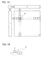
- FIG. 1A illustrates an example of the structure of a semiconductor storage device.
- the semiconductor storage device in FIG. 1A includes a memory cell array 10 in which a plurality of memory cells 20 are arranged in matrix, a row decoder 11 that selects a given row of the memory cell array 10, a column decoder 12 that selects a given column of the memory cell array 10, and a control circuit 13 that selects whether to output a control signal such as an address signal, a read enable signal, or a write enable signal to the row decoder 11 and the column decoder 12.
- a control signal such as an address signal, a read enable signal, or a write enable signal
- a given memory cell 20 (the shaded memory cell 20 in FIG. 1A ) is selected by selecting a given row and a given column by the row decoder 11 and the column decoder 12 in accordance with a control signal, and a data write operation or a data read operation is performed in the selected memory cell 20.
- FIG. 1B illustrates an example of the structure of the memory cell 20 included in the semiconductor storage device illustrated in FIG. 1A .
- the memory cell 20 illustrated in FIG. 1B includes a transistor 21 whose channel region is formed with an oxide semiconductor (OS) and a circuit 22 including a node that is brought into a floating state when the transistor 21 is turned off.
- OS oxide semiconductor
- the memory cell 20 charge can be held in the node, and the value of the potential of the node can correspond to two-level or multilevel data.
- the node is electrically connected to one of a source and a drain of the transistor 21.
- the potential of the node can be easily controlled by transfer of charge through the transistor 21.
- the memory cell 20 can be easily used as a multi-level cell that can store more than one bit of data.
- data stored in the node is less affected by a specific semiconductor element than in flash memory and the like described above.
- the memory cell 20 can store data without largely depending on variations in characteristics of semiconductor elements. Consequently, the potential of the node can be divided into multiple sections to be used as data stored in the memory cell 20.
- data to be stored in the memory cell 20 can have four levels by setting the potentials of the node at 0 V, 0.25 V, 0.5 V, and 0.75 V instead of 0 V, 1 V, 2 V, and 3 V.
- a base layer 91 formed of a stack of a 100-nm-thick silicon nitride layer and a 150-nm-thick silicon oxynitride layer was formed by CVD over a glass substrate 90 (see FIG. 2A ).
- tungsten layer was formed by sputtering over the base layer 91. Then, the tungsten layer was selectively etched by photolithography to form a gate layer 92 (see FIG. 2B ).
- a gate insulating film 93 made of a 100-nm-thick silicon oxynitride layer was formed by CVD over the base layer 91 and the gate layer 92 (see FIG. 2C ).
- a 25-nm-thick oxide semiconductor layer was formed by sputtering over the gate insulating film 93.
- the oxide semiconductor layer was formed under the following conditions: the substrate temperature was 200 °C, the internal pressure of the chamber was 0.6 Pa, the direct-current power was 5 kW, and the atmosphere was a mixed atmosphere of oxygen and argon (the oxygen flow rate was 50 sccm and the argon flow rate was 50 sccm). Then, the oxide semiconductor layer was selectively etched by photolithography, so that an oxide semiconductor layer 94 was formed (see FIG. 2D ).
- the gate insulating film 93 was selectively etched by photolithography (not illustrated). Note that this etching is a step for forming a contact hole for connecting the gate layer 92 and a conductive layer to be formed.
- a stack of a 100-nm-thick titanium layer, a 200-nm-thick aluminum layer, and a 100-nm-thick titanium layer was formed by sputtering over the gate insulating film 93 and the oxide semiconductor layer 94. Then, the stack was selectively etched by photolithography, so that a source layer 95a and a drain layer 95b were formed (see FIG. 2E ).
- a protective insulating layer 96 made of a 300-nm-thick silicon oxide layer was formed over the gate insulating film 93, the oxide semiconductor layer 94, the source layer 95a, and the drain layer 95b. Then, the protective insulating layer 96 was selectively etched by photolithography (see FIG. 2F ). Note that this etching is a step for forming a contact hole for connecting the gate layer, the source layer, and the drain layer and the conductive layer to be formed.
- a 1.5- ⁇ m-thick acrylic layer was applied over the protective insulating layer 96 and selectively exposed to light, so that a planarization insulating layer 97 was formed (see FIG. 2G ). Then, the planarization insulating layer 97 formed of the acrylic layer was baked with heat treatment at 250 °C for one hour in a nitrogen atmosphere.
- a 200-nm-thick titanium layer was formed by sputtering over the planarization insulating layer 97. Then, the titanium layer was selectively etched by photolithography, thereby forming a conductive layer (not illustrated) connected to the gate layer 92, a conductive layer 98a connected to the source layer 95a, and a conductive layer 98b connected to the drain layer 95b (see FIG. 2H ).
- the transistor used for the measurement was formed.
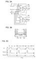
- FIGS. 3A to 3C are diagrams for explaining a circuit for evaluating characteristics.
- FIG. 3A is a circuit diagram illustrating the configuration of the circuit for evaluating characteristics.
- the circuit for evaluating characteristics illustrated in FIG. 3A includes a plurality of measurement systems 801.
- the plurality of measurement systems 801 are connected in parallel with each other.
- eight measurement systems 801 are connected in parallel with each other.
- a plurality of leakage currents can be measured at the same time.
- the measurement system 801 includes a transistor 811, a transistor 812, a capacitor 813, a transistor 814, and a transistor 815.
- the transistors 811, 812, 814. and 815 are n-channel field effect transistors.
- a voltage V1 is input to one of a source and a drain of the transistor 811.
- a voltage Vext_a is input to a gate of the transistor 811.
- the transistor 811 is a transistor for injecting charge.
- One of a source and a drain of the transistor 812 is connected to the other of the source and the drain of the transistor 811.
- a voltage V2 is input to the other of the source and the drain of the transistor 812.
- a voltage Vext_b is input to a gate of the transistor 812.
- the transistor 812 is a transistor for evaluating leakage current. Note that the term "leakage current” here refers to a leakage current including an off-state current of the transistor.
- One electrode of the capacitor 813 is connected to the other of the source and the drain of the transistor 811.
- the voltage V2 is input to the other electrode of the capacitor 813.
- the voltage V2 is 0 V.
- a voltage V3 is input to one of a source and a drain of the transistor 814.
- a gate of the transistor 814 is connected to the other of the source and the drain of the transistor 811. Note that a portion where the gate of the transistor 814, the other of the source and the drain of the transistor 811, the one of the source and the drain of the transistor 812, and the one electrode of the capacitor 813 are connected to each other is referred to as a node A.
- the voltage V3 is 5 V.
- One of a source and a drain of the transistor 815 is connected to the other of the source and the drain of the transistor 814.
- a voltage V4 is input to the other of the source and the drain of the transistor 815.
- a voltage Vext_c is input to a gate of the transistor 815.
- the voltage Vext_c is 0.5 V.
- the measurement system 801 outputs a voltage at a portion where the other of the source and the drain of the transistor 814 is connected to the one of the source and the drain of the transistor 815, as an output voltage Vout.
- the transistor 811 a transistor that is formed by the fabrication method described with reference to FIGS. 2A to 2H and has a channel length L of 10 ⁇ m and a channel width W of 10 ⁇ m is used.
- transistors 814 and 815 a transistor that is formed by the fabrication method described with reference to FIGS. 2A to 2H and has a channel length L of 3 ⁇ m and a channel width W of 100 ⁇ m is used.
- At least the transistor 812 includes a 1- ⁇ m-wide offset region in which the gate layer 92 does not overlap with the source layer 95a and the drain layer 95b as illustrated in FIG. 3B .
- the offset region By providing the offset region, parasitic capacitance can be reduced.
- six samples (SMP) of transistors having different channel lengths L and channel widths W are used (see Table 1).
- the transistor for injecting charge and the transistor for evaluating leakage current are separately provided as illustrated in FIG. 3A , so that the transistor for evaluating leakage current can be always kept off while charge is injected.
- the transistor for injecting charge and the transistor for evaluating leakage current are separately provided, whereby each transistor can have an appropriate size.
- the channel width W of the transistor for evaluating leakage current is made larger than that of the transistor for injecting charge, leakage current components of the circuit for evaluating characteristics other than the leakage current of the transistor for evaluating leakage current can be made relatively small.
- the leakage current of the transistor for evaluating leakage current can be measured with high accuracy.
- the transistor for evaluating leakage current does not need to be turned on at the time of charge injection, the measurement is not adversely affected by variation in the voltage of the node A, which is caused when part of charge in the channel region flows into the node A.
- FIG. 3C is a timing chart for explaining the method for measuring a leakage current with the use of the circuit for evaluating characteristics illustrated in FIG. 3A .
- a write period and a retention period are provided. The operation in each period is described below.
- a voltage VL (-3 V) with which the transistor 812 is turned off is input as the voltage Vext_b.
- a write voltage Vw is input as the voltage Vl
- a voltage VH (5 V) with which the transistor 811 is turned on is input as the voltage Vext_a for a given period of time.
- charge is accumulated in the node A, and the voltage of the node A becomes equivalent to the write voltage Vw.
- the voltage VL with which the transistor 811 is turned off is input as the voltage Vext_a.
- a voltage VSS (0 V) is input as the voltage V1.
- the amount of change in the voltage of the node A which is caused by change in the amount of the charge held in the node A, is measured. From the amount of change in the voltage, the value of the current flowing between the source and the drain of the transistor 812 can be calculated. In the above manner, charge can be accumulated in the node A, and the amount of change in the voltage of the node A can be measured.
- Accumulation of charge in the node A and measurement of the amount of change in the voltage of the node A are repeatedly performed.
- a first accumulation and measurement operation is repeated 15 times.
- a voltage of 5 V is input as the write voltage Vw in the write period and retained for 1 hour in the retention period.
- a second accumulation and measurement operation is repeated twice.
- a voltage of 3.5 V is input as the write voltage Vw in the write period and retained for 50 hours in the retention period.
- a third accumulation and measurement operation is performed once.
- a voltage of 4.5 V is input as the write voltage Vw in the write period and retained for 10 hours in the retention period.
- the measured current value can be confirmed to be the value in the steady state.
- the transient current a current component that decreases over time after the measurement starts
- the leakage current can be measured with higher accuracy.
- a voltage V A of the node A is expressed as a function of the output voltage Vout by Formula 1.
- Charge Q A of the node A is expressed by Formula 2, using the voltage V A of the node A, capacitance C A connected to the node A, and a constant ( const ).
- the capacitance C A connected to the node A is the sum of the capacitance of the capacitor 813 and a capacitance other than that of the capacitor 813.
- the current I A of the node A is the time differential of charge flowing into the node A (or charge flowing from the node A), the current I A of the node A is expressed by Formula 3.
- the current I A of the node A which is the leakage current
- the capacitance C A connected to the node A and the output voltage Vout so that the leakage current of the circuit for evaluating characteristics can be obtained.
- FIG. 4A shows the relation between the elapsed time Time of the above measurement (the first accumulation and measurement operation) of the transistors SMP4, SMP5, and SMP6 and the output voltage Vout.
- FIG. 4B shows the relation between the elapsed time Time of the above measurement and the current I A calculated by the measurement. It is found that the output voltage Vout varies after the measurement starts and it takes 10 hours or longer to reach a steady state.
- FIG. 5 shows the relation between the voltage of the node A in SMP1 to SMP6 and the leakage current estimated by the above measurement.
- SMP4 in FIG. 5 for example, when the voltage of the node A is 3.0 V, the leakage current (per unit channel width (1 ⁇ m) here) is 28 yA/ ⁇ m. Since the leakage current includes the off-state current of the transistor 812, the off-state current of the transistor 812 can be considered to be 28 yA/ ⁇ m or less.
- FIG. 6 , FIG. 7 , and FIG. 8 each show the relation between the voltage of the node A in SMP1 to SMP6 at 85 °C, 125 °C, and 150 °C and the leakage current estimated by the above measurement. As shown in FIGS. 6 to 8 , the leakage current is 100 zA/ ⁇ m or less even at 150 °C.
- the leakage current is sufficiency low in the circuit for evaluating characteristics, which includes the transistor whose channel region is formed with an oxide semiconductor. This means that the off state current of the transistor is sufficiently low. In addition, the off-state current of the transistor is sufficiently low even when the temperature rises.
- data is stored by turning off a selection transistor whose channel region is formed with an oxide semiconductor in each of a plurality of memory cells.
- stored data can be retained for a long time even when power is not supplied (note that the potentials of wirings are preferably fixed).
- the semiconductor storage device disclosed in this specification does not need high voltage for writing data, and there is no problem of degradation of the element.
- the semiconductor storage device disclosed in this specification does not have a limitation on the number of rewrite cycles, which has been a problem of a conventional non-volatile memory, and thus has significantly improved reliability.
- the semiconductor storage device since data is written by switching of the transistor, high-speed operation can be easily realized.
- the semiconductor storage device has an advantage of not needing an operation for erasing data.
- the semiconductor storage device disclosed in this specification includes a control circuit that selects whether to output a control signal to a decoder for selecting a desired memory cell. Consequently, malfunction of the decoder can be suppressed even when noise is generated in wirings at the time of turning on the power, for example. Thus, data rewriting errors can be suppressed.
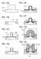
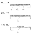
- FIGS. 9A to 9C Specific examples of the above-described semiconductor storage device will be described with reference to FIGS. 9A to 9C , FIGS. 10A to 10D , FIGS. 11A and 11B , FIG. 12 , FIGS. 13A to 13H , FIGS. 14A to 14G , FIGS. 15A to 15D , FIG. 16 , FIGS. 17A and 17B , FIGS. 18A and 18B , FIGS. 19A and 19B , FIG. 20 , FIG. 21 , and FIGS. 22A to 22C .
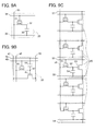
- FIG. 9A is a circuit diagram illustrating a specific example of the memory cell 20.
- the memory cell 20 illustrated in FIG. 9A includes a transistor 31 and a capacitor 33.
- a gate of the transistor 31 is electrically connected to a word line 34.
- One of a source and a drain of the transistor 31 is electrically connected to a bit line 35.
- One electrode of the capacitor 33 is electrically connected to the other of the source and the drain of the transistor 31.
- the other electrode of the capacitor 33 is electrically connected to a wiring 36 that supplies a fixed potential.
- data is stored in a node 32 where the other of the source and the drain of the transistor 31 and the one electrode of the capacitor 33 are electrically connected to each other.
- As the fixed potential a ground potential (GND), 0 V, or the like can be employed.
- GND ground potential
- the value of the potential of the node 32 can correspond directly to two-level or multilevel data. Specifically, the potential of the bit line 35 at the time of reading during which the transistor 31 is on varies depending on the amount of charge held in the capacitor 33; therefore, data held in the memory cell 20 can be judged from the value of the potential of the bit line at the time of reading.
- FIG. 9B is a circuit diagram illustrating a specific example of the memory cell 20, which is different from that in FIG. 9A .
- the memory cell 20 illustrated in FIG. 9B includes a transistor 41, a transistor 43, and a capacitor 44.
- a gate of the transistor 41 is electrically connected to a writing word line 45.
- One of a source and a drain of the transistor 41 is electrically connected to a writing bit line 48.
- a gate of the transistor 43 is electrically connected to the other of the source and the drain of the transistor 41.
- One of a source and a drain of the transistor 43 is electrically connected to a reading bit line 47.
- the other of the source and the drain of the transistor 43 is electrically connected to a wiring 49 that supplies a fixed potential.
- One electrode of the capacitor 44 is electrically connected to the other of the source and the drain of the transistor 41 and the gate of the transistor 43.
- the other electrode of the capacitor 44 is electrically connected to a reading word line 46.
- data is stored in a node 42 where the other of the source and the drain of the transistor 41, the gate of the transistor 43, and the one electrode of the capacitor 44 are electrically connected to each other.
- a ground potential (GND), 0 V or the like can be employed.
- the transistor 41 is a transistor whose channel region is formed with an oxide semiconductor (OS).
- OS oxide semiconductor
- switching of the transistor 43 can be controlled in accordance with the potential of the node 42.
- the potential of the node 42 can be controlled by capacitive coupling with the reading word line 46.
- multilevel data can be stored in the memory cell 20 in FIG. 9B .
- the conduction state (the on state or the off state) of the transistor 43 under a plurality of conditions with different potentials of the reading word line 46 data can be read out even when the potential of the node 42 is a multivalued potential.
- data can be read out by, for example, judging an output signal of a voltage divider circuit constituted by the transistor 43.
- the memory cell 20 in FIG. 9B can also be used as a memory cell that retains binary data.
- FIG. 9C is a circuit diagram illustrating a specific example of the memory cell 20, which is different from the examples in FIGS. 9A and 9B .
- the memory cell 20 in FIG. 9C is one of n memory cells arranged in one column.
- the memory cell 20 includes a transistor 51, a transistor 53, and a capacitor 54.
- a gate of the transistor 51 is electrically connected to a writing word line 55.
- One of a source and a drain of the transistor 51 is electrically connected to a writing bit line 58.
- a gate of the transistor 53 is electrically connected to the other of the source and the drain of the transistor 51.
- One electrode of the capacitor 54 is electrically connected to the other of the source and the drain of the transistor 51 and the gate of the transistor 53.
- the other electrode of the capacitor 54 is electrically connected to a reading word line 56.
- one of the source and the drain of the transistor 53 in the k -th memory cell 20 ( k is a natural number greater than or equal to 2 and less than n ) is electrically connected to the other of the source and the drain of the transistor 53 in the ( k -1)th memory cell 20.
- the other of the source and the drain of the transistor S3 in the k -th memory cell 20 is electrically connected to one of the source and the drain of the transistor 53 in the ( k +1)th memory cell 20.
- One of the source and the drain of the transistor 53 in the first memory cell 20 is electrically connected to a wiring 59 that supplies a fixed potential.
- the other of the source and the drain of the transistor 53 in the n -th memory cell 20 is electrically connected to a reading bit line 57.
- the transistor 51 is a transistor whose channel region is formed with an oxide semiconductor (OS).
- OS oxide semiconductor
- switching of the transistor 53 can be controlled in accordance with the potential of the node 52.
- the potential of the node 52 can be controlled by capacitive coupling with the reading word line 56. Note that in a semiconductor storage device including the memory cell 20 illustrated in FIG. 9C , in order to read data stored in any one of n memory cells 20 arranged in one column, the potentials of the reading word lines 56 connected to ( n -1) memory cells 20 other than the memory cell 20 subjected to data reading are raised to high level. Thus, the transistors 53 included in the ( n -1) memory cells 20 other than the memory cell 20 subjected to data reading are turned on.
- stored data can be obtained by judging the state (the on state or the off state) of the transistor 53 in the memory cell 20 subjected to data reading.
- stored data can be obtained in such a manner that, for example, a voltage divider circuit is constituted by the transistor 53 included in the memory cell 20 subjected to data reading and an output signal of the voltage divider circuit is judged. Note that in order to judge multilevel data in the memory cell 20 in FIG.
- the state (the on state or the off state) of the transistor 53 needs to be judged under a plurality of conditions with different potentials of the reading word line 56.
- the memory cell 20 in FIG. 9C can also be used as a memory cell that stores binary data.
- FIGS. 10A to 10C are circuit diagrams each illustrating a specific example of the control circuit 13.
- each of the control circuits 13 illustrated in FIGS. 10A to 10C is a circuit that selects whether to output control signals input from the outside (in FIGS. 10A to 10C , an address signal (ADDR_in), a read control signal (RE_in), and a write control signal (WE_in) correspond to such control signals) to the row decoder and the column decoder in accordance with a reset signal (RESET).
- ADDR_in address signal
- RE_in read control signal
- WE_in write control signal
- control circuit 13 does not output a control signal to the row decoder and the column decoder in a given period when power supply starts and outputs a control signal after the given period passes. In that case, it is preferable that the control circuit 13 do not output a control signal to the row decoder and the column decoder in a period during which the reset signal (RESET) has a ground potential (GND).
- REET reset signal
- GND ground potential
- each of the control circuits 13 illustrated in FIGS. 10A to 10C is a digital circuit whose operation is controlled with a low-level potential that is the ground potential (GND) and a high-level potential that is higher than the ground potential (GND).
- the control circuit 13 in FIG. 10A includes an inverter 61, a switch 62, a switch 63, and a switch 64.
- An input terminal of the inverter 61 is electrically connected to a wiring that supplies the reset signal (RESET).
- An input terminal of the switch 62 is electrically connected to a wiring that supplies the address signal (ADDR_in).
- An input terminal of the switch 63 is electrically connected to a wiring that supplies the read control signal (RE_in).
- An input terminal of the switch 64 is electrically connected to a wiring that supplies the write control signal (WE_in).
- the switches 62 to 64 are designed so that they are turned on when the potential of the reset signal (RESET) is set at high level and are turned off when the potential of the reset signal (RESET) is set at low level. Therefore, the control circuit 13 in FIG. 10A outputs control signals to the row decoder and the column decoder when the reset signal (RESET) has a high-level potential, and makes the potentials of the wirings that supply the control signals to the row decoder and the column decoder floating when the reset signal (RESET) has a low-level potential.
- the control circuit 13 illustrated in FIG. 10A is preferable to the control circuits 13 illustrated in FIGS. 10B and 10C in that the number of transistors necessary for constituting the circuit is smaller.
- the control circuit 13 in FIG. 10B includes an AND gate 66, an AND gate 67, and an AND gate 68.
- a first input terminal of the AND gate 66 is electrically connected to a wiring that supplies the reset signal (RESET).
- a second input terminal of the AND gate 66 is electrically connected to a wiring that supplies the address signal (ADDR_in).
- a first input terminal of the AND gate 67 is electrically connected to the wiring that supplies the reset signal (RESET).
- a second input terminal of the AND gate 67 is electrically connected to a wiring that supplies the read control signal (RE_in).
- a first input terminal of the AND gate 68 is electrically connected to the wiring that supplies the reset signal (RESET).
- a second input terminal of the AND gate 68 is electrically connected to a wiring that supplies the write control signal (WE_in). Therefore, the control circuit 13 in FIG. 10B outputs control signals to the row decoder and the column decoder when the potential of the reset signal (RESET) is set at high level, and sets the potentials of the wirings that supply the control signals to the row decoder and the column decoder at low level when the potential of the reset signal (RESET) is set at low level.
- the control circuit 13 in FIG. 10B is preferable in that the potentials of the wirings that supply the control signals to the row decoder and the column decoder are not made floating, which means that the probability of malfunction occurring in the row decoder and the column decoder can be further reduced.
- the control circuit 13 in FIG. 10C includes a flip-flop 69 to which control signals (the address signal (ADDR_in), the write control signal (WE_in), and the read control signal (RE_in) in FIG. 10C ), a clock signal (CK), and the reset signal (RESET) are input.
- the flip-flop 69 in FIG. 10C outputs the control signals in accordance with the cycle of the clock signal when the potential of the reset signal (RESET) is set at high level, and sets the potentials of the wirings that supply the control signals to the row decoder and the column decoder at low level when the potential of the reset signal (RESET) is set at low level.
- the control circuit 13 in FIG. 10C is preferable in that the potentials of the wirings that supply the control signals to the row decoder and the column decoder are not made floating, which means that the probability of malfunction occurring in the row decoder and the column decoder can be further reduced.
- FIG. 10D is a timing chart illustrating a specific example of the operation of the control circuits 13 illustrated in FIGS. 10A to 10C .
- a reset period during which the reset signal (RESET) has a low-level potential is provided over a given period after power supply starts. Accordingly, even if the potentials of the wirings that supply the control signals (the address signal (ADDR_in), the read control signal (RE_in), and the write control signal (WE_in)) to the control circuit 13 are varied by noise generated when power supply starts, the potentials of these wirings are not input to the row decoder and the column decoder. In other words, malfunction of the row decoder and the column decoder can be suppressed.
- control circuit 13 ⁇ Second specific example of control circuit 13>
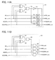
- FIGS. 11A and 11B are circuit diagrams each illustrating a specific example of the control circuit 13.
- the control circuits 13 illustrated in FIGS. 11A and 11B operate as follows.
- the control circuit 13 outputs the control signal and the inverted control signal to the row decoder and the column decoder.
- the control circuit 13 When these signals are not inverse to each other, the control circuit 13 does not output the control signal and the inverted control signal to the row decoder and the column decoder.
- the row decoder and the column decoder select a given memory cell in accordance with the control signal and the inverted control signal.
- control circuit 13 can be a circuit that selects whether to output only the control signal to row decoder and the column decoder depending on the states of the potential of the wiring supplied with the control signal and the potential of the wiring supplied with the inverted control signal (i.e., depending on whether these control signals are inverse to each other).
- the control circuit 13 illustrated in FIG. 11A includes an XOR gate 71, an XOR gate 72, an AND gate 73, an inverter 74, a switch 75, a switch 76, a switch 77, and a switch 78.
- a first input terminal of the XOR gate 71 is electrically connected to a wiring that supplies the read control signal (RE_in).
- a second input terminal of the XOR gate 71 is electrically connected to a wiring that supplies the write control signal (WE_in).
- a first input terminal of the XOR gate 72 is electrically connected to a wiring that supplies the address signal (ADDR_in).
- a second input terminal of the XOR gate 72 is electrically connected to a wiring that supplies the inverted address signal (ADDRB_in).
- a first input terminal of the AND gate 73 is electrically connected to an output terminal of the XOR gate 71.
- a second input terminal of the AND gate 73 is electrically connected to an output terminal of the XOR gate 72.
- An input terminal of the inverter 74 is electrically connected to an output terminal of the AND gate 73.
- An input terminal of the switch 75 is electrically connected to the wiring that supplies the read control signal (RE_in).
- An input terminal of the switch 76 is electrically connected to the wiring that supplies the write control signal (WE_in).
- An input terminal of the switch 77 is electrically connected to the wiring that supplies the address signal (ADDR_in).
- An input terminal of the switch 78 is electrically connected to the wiring that supplies the inverted address signal (ADDRB_in).
- switches 75 to 78 are designed so that they are turned on when the potential of the output signal of the AND gate 73 is set at high level (when the potential of the output signal of the inverter 74 is set at low level) and are turned off when the potential of the output signal of the AND gate 73 is set at low level (when the potential of the output signal of the inverter 74 is set at high level). Therefore, the control circuit 13 in FIG.
- 11A outputs the read control signal (RE_in), the write control signal (WE_in), the address signal (ADDR_in), and the inverted address signal (ADDRB_in) to the row decoder and the column decoder in the case where only one of the potential of the wiring supplying the read control signal (RE_in) and the potential of the wiring supplying the write control signal (WE_in) is a high-level potential and the potential of the wiring supplying the address signal (ADDR_in) is the inverse of the potential of the wiring supplying the inverted address signal (ADDRB_in), and makes the potentials of the wirings that supply these signals to the row decoder and the column decoder floating when the above conditions are not satisfied.
- control circuit 13 in FIG. 11A the probability of malfunction occurring in the row decoder and the column decoder can be reduced even if the potential of the wiring that supplies one of the read control signal (RE_in), the write control signal (WE_in), the address signal (ADDR_in), and the inverted address signal (ADDRB_in) is varied by noise or the like. Further, the control circuit 13 in FIG. 11A is preferable to the control circuit 13 in FIG. 11B in that the number of transistors necessary for constituting the circuit is smaller.
- the control circuit 13 illustrated in FIG. 11B includes an XOR gate 81, an XOR gate 82, an AND gate 83, an AND gate 84, an AND gate 85, an AND gate 86, and an AND gate 87.
- a first input terminal of the XOR gate 81 is electrically connected to a wiring that supplies the read control signal (RE_in).
- a second input terminal of the XOR gate 81 is electrically connected to a wiring that supplies the write control signal (WE_in).
- a first input terminal of the XOR gate 82 is electrically connected to a wiring that supplies the address signal (ADDR_in).
- a second input terminal of the XOR gate 82 is electrically connected to a wiring that supplies the inverted address signal (ADDRB_in).
- a first input terminal of the AND gate 83 is electrically connected to an output terminal of the XOR gate 81.
- a second input terminal of the AND gate 83 is electrically connected to an output terminal of the XOR gate 82.
- a first input terminal of the AND gate 84 is electrically connected to an output terminal of the AND gate 83.
- a second input terminal of the AND gate 84 is electrically connected to the wiring that supplies the read control signal (RE_in).
- a first input terminal of the AND gate 85 is electrically connected to the output terminal of the AND gate 83.
- a second input terminal of the AND gate 85 is electrically connected to the wiring that supplies the write control signal (WE_in).
- a first input terminal of the AND gate 86 is electrically connected to the output terminal of the AND gate 83.
- a second input terminal of the AND gate 86 is electrically connected to the wiring that supplies the address signal (ADDR_in).
- a first input terminal of the AND gate 87 is electrically connected to the output terminal of the AND gate 83.
- a second input terminal of the AND gate 87 is electrically connected to the wiring that supplies the inverted address signal (ADDRB_in).
- the control circuit 13 in FIG. 11B outputs the read control signal (RE_in), the write control signal (WE_in), the address signal (ADDR_in), and the inverted address signal (ADDRB_in) to the row decoder and the column decoder in the case where only one of the potential of the wiring supplying the read control signal (RE_in) and the potential of the wiring supplying the write control signal (WE_in) is a high-level potential and the potential of the wiring supplying the address signal (ADDR_in) is the inverse of the potential of the wiring supplying the inverted address signal (ADDRB_in), and sets the potentials of the wirings that supply these signals to the row decoder and the column decoder at low level when the above conditions are not satisfied.
- control circuit 13 in FIG. 11B is preferable in that the potentials of the wirings that supply the control signals to the row decoder and the column decoder are not made floating. Thus, the probability of malfunction occurring in the row decoder and the column decoder can be further reduced.
- transistors included in the semiconductor storage device will be described below. Specifically, an example of the case where a transistor formed using a substrate containing a semiconductor material and a transistor formed using an oxide semiconductor will be described.
- a transistor 160 illustrated in FIG. 12 includes a channel region 116 provided in a substrate 100 containing a semiconductor material, a pair of impurity regions 114a and 114b and a pair of high concentration impurity regions 120a and 120b (these regions are also collectively referred to simply as impurity regions) provided so that the channel region 116 is placed therebetween, a gate insulating film 108a provided over the channel region 116, a gate layer 110a provided over the gate insulating film 108a, a source layer 130a electrically connected to the impurity region 114a, and a drain layer 130b electrically connected to the impurity region 114b.
- sidewall insulating layers 118 are provided on side surfaces of the gate layer 110a.
- the pair of high concentration impurity regions 120a and 120b is placed in regions that do not overlap with the sidewall insulating layers 118.
- a pair of metal compound regions 124a and 124b is placed on the pair of high concentration impurity regions 120a and 120b.
- An element isolation insulating layer 106 is provided over the substrate 100 so as to surround the transistor 160.
- An interlayer insulating layer 126 and an interlayer insulating layer 128 are provided so as to cover the transistor 160.
- the source layer 130a is electrically connected to the metal compound region 124a through an opening formed in the interlayer insulating layers 126 and 128.
- the drain layer 130b is electrically connected to the metal compound region 124b through an opening formed in the interlayer insulating layers 126 and 128. That is, the source layer 130a is electrically connected to the high concentration impurity region 120a and the impurity region 114a through the metal compound region 124a, and the drain layer 130b is electrically connected to the high concentration impurity region 120b and the impurity region 114b through the metal compound region 124b.
- an insulating layer 108b using the same material as the gate insulating film 108a, an electrode layer 110b using the same material as the gate layer 110a, and an electrode layer 130c using the same material as the source layer 130a and the drain layer 130b are provided below a transistor 164 described later.
- the transistor 164 illustrated in FIG. 12 includes a gate layer 136d provided over the interlayer insulating layer 128, a gate insulating film 138 provided over the gate layer 136d, an oxide semiconductor layer 140 provided over the gate insulating film 138, and a source layer 142a and a drain layer 142b that are provided over the oxide semiconductor layer 140 and electrically connected to the oxide semiconductor layer 140.
- the gate layer 136d is provided to be embedded in an insulating layer 132 formed over the interlayer insulating layer 128. Like the gate layer 136d, an electrode layer 136a and an electrode layer 136b that are included in the transistor 160 and are in contact with the source layer 130a and the drain layer 130b, respectively, are formed. In addition, an electrode layer 136c in contact with the electrode layer 130c is formed.
- a protective insulating layer 144 is provided over the transistor 164 so as to be in contact with part of the oxide semiconductor layer 140.
- An interlayer insulating layer 146 is provided over the protective insulating layer 144.
- openings reaching the source layer 142a and the drain layer 142b are provided in the protective insulating layer 144 and the interlayer insulating layer 146.
- An electrode layer 150d in contact with the source layer 142a and an electrode layer 150e in contact with the drain layer 142b are formed through the openings.
- an electrode layer 150a in contact with the electrode layer 136a, an electrode layer 150b in contact with the electrode layer 136b, and an electrode layer 150c in contact with the electrode layer 136c are formed through openings provided in the gate insulating film 138, the protective insulating layer 144, and the interlayer insulating layer 146.
- the oxide semiconductor layer 140 is highly purified by sufficient removal of impurities such as hydrogen. Specifically, the hydrogen concentration of the oxide semiconductor layer 140 is 5 ⁇ 10 19 (atoms/cm 3 ) or lower. Note that the hydrogen concentration of the oxide semiconductor layer 140 is preferably 5 ⁇ 10 18 (atoms/cm 3 ) or lower, further preferably 5 ⁇ 10 17 (atoms/cm 3 ) or lower.
- the transistor 164 with excellent off-state current characteristics can be obtained with the use of such an oxide semiconductor layer 140 that is highly purified by a sufficient reduction in hydrogen concentration. For example, when the drain voltage Vd is +1 V or +10 V, the leakage current is 1 ⁇ 10 -13 [A] or less. By using the oxide semiconductor layer 140 which is highly purified by sufficiently reducing the hydrogen concentration, the leakage current of the transistor 164 can be reduced. Note that the hydrogen concentration of the oxide semiconductor layer 140 is measured by secondary ion mass spectrometry (SIMS).
- SIMS secondary ion mass spectrometry
- an insulating layer 152 is provided over the interlayer insulating layer 146, and an electrode layer 154a, an electrode layer 154b, an electrode layer 154c, and an electrode layer 154d are provided so as to be embedded in the insulating layer 152.
- the electrode layer 154a is in contact with the electrode layer 150a; the electrode layer 154b is in contact with the electrode layer 150b; the electrode layer 154c is in contact with the electrode layer 150c and the electrode layer 150d; and the electrode layer 154d is in contact with the electrode layer 150e.
- the source layer 130a included in the transistor 160 in FIG. 12 is electrically connected to the electrode layers 136a, 150a, and 154a which are provided in the upper region.
- the source layer 130a in the transistor 160 can be electrically connected to any of the electrode layers included in the transistor 164 provided in the upper region.
- the drain layer 130b in the transistor 160 can also be electrically connected to any of the electrode layers included in the transistor 164 provided in the upper region.
- the gate layer 110a in the transistor 160 can be electrically connected to any of the electrode layers included in the transistor 164 through an electrode layer provided in the upper region.
- the source layer 142a included in the transistor 164 in FIG. 12 is electrically connected to the electrode layers 130c and 110b provided in the lower region.
- the source layer 142a in the transistor 164 can be electrically connected to any of the gate layer 110a, the source layer 130a, and the drain layer 130b which are included in the transistor 160 provided in the lower region.
- the gate layer 136d or the drain layer 142b in the transistor 164 can be electrically connected to any of the electrode layers included in the transistor 160 through an electrode layer provided in the lower region.
- a method for fabricating the transistor 160 is described first with reference to FIGS. 13A to 13H , and then, a method for fabricating the transistor 164 is described with reference to FIGS. 14A to 14G and FIGS. 15A to 15D .
- the substrate 100 containing a semiconductor material is prepared (see FIG. 13A ).
- a single crystal semiconductor substrate or a polycrystalline semiconductor substrate of silicon, silicon carbide, or the like, a compound semiconductor substrate of silicon germanium or the like, an SOI substrate, or the like can be used.
- an example where a single crystal silicon substrate is used as the substrate 100 containing a semiconductor material is described.
- the "SOI substrate” means a substrate in which a silicon semiconductor layer is provided on an insulating surface.
- the "SOI substrate” also includes a substrate in which a semiconductor layer containing a material other than silicon is provided over an insulating surface in its category.
- a semiconductor layer included in the "SOI substrate” is not limited to a silicon semiconductor layer.
- the "SOI substrate” includes a substrate in which a semiconductor layer is formed over an insulating substrate such as a glass substrate with an insulating layer placed therebetween.
- a protective layer 102 serving as a mask for formation of an element isolation insulating layer is formed over the substrate 100 (see FIG. 13A ).
- an insulating layer formed using silicon oxide, silicon nitride, silicon nitride oxide, or the like can be used, for example.
- an impurity element imparting n-type conductivity or an impurity element imparting p-type conductivity may be added to the substrate 100 in order to control the threshold voltage of a transistor.
- silicon is used as the semiconductor, phosphorus, arsenic, or the like can be used as the impurity imparting n-type conductivity. Boron, aluminum, gallium, or the like can be used as the impurity imparting p-type conductivity.
- part of the substrate 100 which is not covered with the protective layer 102 is removed by etching with the use of the protective layer 102 as a mask.
- an isolated semiconductor region 104 is formed (see FIG. 13B ).
- dry etching is preferably performed, but wet etching may be performed.
- An etching gas or an etchant can be selected as appropriate depending on materials of layers to be etched.
- an insulating layer is formed to cover the semiconductor region 104, and part of the insulating layer which overlaps with the semiconductor region 104 is selectively removed, so that the element isolation insulating layers 106 are formed (see FIG. 13B ).
- the insulating layer is formed using silicon oxide, silicon nitride, silicon nitride oxide, or the like.
- any of polishing treatment such as chemical mechanical polishing (CMP), etching treatment, and the like can be employed.
- CMP chemical mechanical polishing
- the protective layer 102 is removed after the formation of the semiconductor region 104 or after the formation of the element isolation insulating layers 106.
- an insulating layer is formed over the semiconductor region 104, and a layer containing a conductive material is formed over the insulating layer.
- the insulating layer serves as a gate insulating film later, and preferably has a single-layer structure or a stacked structure using a film containing silicon oxide, silicon nitride oxide, silicon nitride, hafnium oxide, aluminum oxide, tantalum oxide, or the like formed by CVD, sputtering, or the like.
- the insulating layer may be formed in such a manner that a surface of the semiconductor region 104 is oxidized or nitrided by high-density plasma treatment or thermal oxidation treatment.
- the high-density plasma treatment can be performed using, for example, a mixed gas of a rare gas such as He, Ar, Kr, or Xe and a gas such as oxygen, nitrogen oxide, ammonia, or nitrogen.
- a mixed gas of a rare gas such as He, Ar, Kr, or Xe
- a gas such as oxygen, nitrogen oxide, ammonia, or nitrogen.
- the thickness of the insulating layer can have a thickness of 1 nm to 100 nm, for example.
- the layer containing a conductive material can be formed using a metal material such as aluminum, copper, titanium, tantalum, or tungsten.
- the layer containing a conductive material may be formed using a semiconductor material such as polycrystalline silicon containing a conductive material.
- a variety of film formation methods such as evaporation, CVD, sputtering, and spin coating can be employed. Note that here, an example of the case where the layer containing a conductive material is formed using a metal material is described.
- the insulating layer and the layer containing a conductive material are selectively etched, so that the gate insulating film 108a and the gate layer 110a are formed (see FIG. 13C ).
- an insulating layer 112 that covers the gate layer 110a is formed (see FIG. 13C ). Then, boron (B), phosphorus (P), arsenic (As), or the like is added to the semiconductor region 104, so that the pair of impurity regions 114a and 114b with a shallow junction is formed (see FIG. 13C ). Note that by formation of the pair of impurity regions 114a and 114b, the channel region 116 is formed in the semiconductor region 104 below the gate insulating film 108a (see FIG. 13C ).
- the concentration of the impurity added can be set as appropriate; the concentration is preferably increased when the size of the semiconductor element is extremely decreased.
- the pair of impurity regions 114a and 114b is formed after formation of the insulating layer 112 here, the insulating layer 112 may be formed after formation of the pair of impurity regions 114a and 114b.
- the sidewall insulating layers 118 are formed (see FIG. 13D ).
- the sidewall insulating layers 118 can be formed in a self-aligned manner by forming an insulating layer so as to cover the insulating layer 112 and then performing highly anisotropic etching on the insulating layer. At this time, by partial etching of the insulating layer 112, an upper surface of the gate layer 110a and upper surfaces of the pair of impurity regions 114a and 114b are preferably exposed.
- an insulating layer is formed so as to cover the gate layer 110a, the pair of impurity regions 114a and 114b, the sidewall insulating layers 118, and the like. Then, boron (B), phosphorus (P), arsenic (As), or the like is added to part of the impurity regions 114a and 114b, whereby the pair of high concentration impurity regions 120a and 120b is formed (see FIG. 13E ). After that, the insulating layer is removed, and a metal layer 122 is formed so as to cover the gate layer 110a, the sidewall insulating layers 118, the pair of high concentration impurity regions 120a and 120b, and the like (see FIG. 13E ).
- the metal layer 122 can be formed by a variety of film formation methods such as vacuum evaporation, sputtering, and spin coating.
- the metal layer 122 is preferably formed using a metal material that reacts with a semiconductor material included in the semiconductor region 104 to be a low-resistance metal compound. Examples of such metal materials are titanium, tantalum, tungsten, nickel, cobalt, and platinum.
- the pair of metal compound regions 124a and 124b in contact with the pair of high concentration impurity regions 120a and 120b is formed (see FIG. 13F ). Note that when the gate layer 110a is formed using polycrystalline silicon or the like, a metal compound region is also formed in a region of the gate layer 110a in contact with the metal layer 122.
- the heat treatment irradiation with a flash lamp can be employed, for example.
- a method by which heat treatment for an extremely short time can be achieved is preferably used in order to improve the controllability of chemical reaction for formation of the metal compound.
- the metal compound regions are formed by reaction of the metal material and the semiconductor material and have sufficiently high conductivity. The formation of the metal compound regions can properly reduce the electric resistance and improve element characteristics. Note that the metal layer 122 is removed after the pair of metal compound regions 124a and 124b is formed.
- the interlayer insulating layer 126 and the interlayer insulating layer 128 are formed so as to cover the components formed in the above steps (see FIG. 13G ).
- the interlayer insulating layers 126 and 128 can be formed using an inorganic insulating material such as silicon oxide, silicon nitride oxide, silicon nitride, hafnium oxide, aluminum oxide, or tantalum oxide.
- the interlayer insulating layers 126 and 128 can be formed using an organic insulating material such as polyimide or acrylic. Note that the interlayer insulating layer has a two-layer structure of the interlayer insulating layer 126 and the interlayer insulating layer 128 here; it is not limited to having this structure.
- a surface of the interlayer insulating layer 128 is preferably planarized with CMP, etching, or the like.
- the source layer 130a and the drain layer 130b can be formed in such a manner, for example, that a conductive layer is formed in a region including the openings by PVD, CVD, or the like and then part of the conductive layer is removed by etching or CMP.
- the source layer 130a and the drain layer 130b be formed to have a planar surface.
- a thin titanium film or a thin titanium nitride film is formed in a region including the openings and then a tungsten film is formed to be embedded in the openings, excess tungsten, titanium, titanium nitride, or the like is removed and the planarity of the surface can be improved by subsequent CMP.
- the surface including the source layer 130a and the drain layer 130b is planarized, whereby an electrode, a wiring, an insulating layer, a semiconductor layer, and the like can be favorably formed in later steps.
- the electrode layer serving as a wiring e.g., the electrode layer 130c in FIG. 12
- the electrode layer serving as a wiring e.g., the electrode layer 130c in FIG. 12
- a material used for the source layer 130a and the drain layer 130b and a variety of conductive materials can be used.
- a conductive material such as molybdenum, titanium, chromium, tantalum, tungsten, aluminum, copper, neodymium, or scandium can be used.
- an alloy containing at least one of these conductive materials can be used.
- an alloy that contains copper as its main component and also contains magnesium and aluminum can be used.
- the transistor 160 using the substrate 100 containing a semiconductor material is formed.
- an electrode, a wiring, an insulating layer, or the like may be further formed after the above step.
- the wiring has a multilayer wiring structure which is a stacked structure including an interlayer insulating layer and a conductive layer, a highly integrated circuit can be provided.
- FIGS. 14A to 14G and FIGS. 15A to 15D illustrate steps for forming various electrode layers, the transistor 164, and the like over the interlayer insulating layer 128; therefore, the transistor 160 and the like placed below the transistor 164 are omitted.
- the insulating layer 132 is formed over the interlayer insulating layer 128, the source layer 130a, the drain layer 130b, and the electrode layer 130e (see FIG. 14A ).
- the insulating layer 132 can be formed by PVD, CVD, or the like.
- the insulating layer 132 can be formed using an inorganic insulating material such as silicon oxide, silicon nitride oxide, silicon nitride, hafnium oxide, aluminum oxide, or tantalum oxide.
- openings that reach the source layer 130a, the drain layer 130b, and the electrode layer 130c are formed in the insulating layer 132. At this time, an opening is also formed in a region where the gate layer 136d is to be formed later. Then, a conductive layer 134 is formed so as to fill the openings ( FIG. 14B ).
- the openings can be formed by etching using a mask or the like.
- the mask can be formed by light exposure using a photomask or the like. Either wet etching or dry etching may be used as the etching; dry etching is preferably used in terms of microfabrication.
- the conductive layer 134 can be formed by a film formation method such as PVD or CVD.
- the conductive layer 134 can be formed using a conductive material such as molybdenum, titanium, chromium, tantalum, tungsten, aluminum, copper, neodymium, or scandium or an alloy or a compound (e.g., a nitride) of any of these materials, for example.
- a conductive material such as molybdenum, titanium, chromium, tantalum, tungsten, aluminum, copper, neodymium, or scandium or an alloy or a compound (e.g., a nitride) of any of these materials, for example.
- a method for example, in which a thin titanium film is formed in a region including the openings by PVD and a thin titanium nitride film is formed by CVD, and then, a tungsten film is formed to fill the openings.
- the titanium film formed by PVD has a function of deoxidizing an oxide film at an interface so as to reduce contact resistance with the lower electrode layers (here, the source layer 130a, the drain layer 130b, the electrode layer 130c, and the like).
- the titanium nitride film formed after the formation of the titanium film has a barrier function of preventing diffusion of the conductive material.
- a copper film may be formed by plating after the formation of the barrier film of titanium, titanium nitride, or the like.
- part of the conductive layer 134 is removed by etching, CMP, or the like, whereby the insulating layer 132 is exposed and the electrode layers 136a, 136b, and 136c and the gate layer 136d are formed (see FIG. 14C ).
- the process is preferably performed so that the surfaces are planarized.
- the surfaces of the insulating layer 132, the electrode layers 136a to 136c, and the gate layer 136d are planarized in such a manner, whereby an electrode, a wiring, an insulating layer, a semiconductor layer, and the like can be favorably formed in later steps.
- the gate insulating film 138 is formed so as to cover the insulating layer 132, the electrode layers 136a to 136c, and the gate layer 136d (see FIG. 14D ).
- the gate insulating film 138 can be formed by CVD, sputtering, or the like. It is preferable that the gate insulating film 138 contain silicon oxide, silicon nitride, silicon oxynitride, silicon nitride oxide, aluminum oxide, hafnium oxide, tantalum oxide, or the like. Note that the gate insulating film 138 may have a single-layer structure or a stacked structure.
- the gate insulating film 138 made of silicon oxynitride can be formed by plasma-enhanced CVD using silane (SiH 4 ), oxygen, and nitrogen as a source gas.
- the thickness of the gate insulating film 138 there is no particular limitation on the thickness of the gate insulating film 138; the gate insulating film 138 can have a thickness of 10 nm to 500 nm, for example.
- the gate insulating film 138 is preferably a stack of a first gate insulating film with a thickness of 50 nm to 200 nm, and a second gate insulating film with a thickness of 5 nm to 300 nm over the first gate insulating film.
- an oxide semiconductor which is made to be an i-type oxide semiconductor or a substantially i-type oxide semiconductor by removing an impurity is extremely sensitive to an interface state or to the interface charge; thus, when such an oxide semiconductor is used for an oxide semiconductor layer, the interface between the oxide semiconductor layer and the gate insulating film is important.
- the gate insulating film 138 that is to be in contact with a highly purified oxide semiconductor layer needs to have high quality.
- high-density plasma-enhanced CVD using microwaves (2.45 GHz) is preferable because the gate insulating film 138 can be dense and have high withstand voltage and high quality.
- the highly purified oxide semiconductor layer and the high-quality gate insulating film are in close contact with each other, so that interface state density can be reduced and favorable interface characteristics can be obtained.
- an oxide semiconductor layer is formed over the gate insulating film 138 and processed by etching using a mask or the like, whereby the island-shaped oxide semiconductor layer 140 is formed (see FIG. 14E ).
- the oxide semiconductor layer contains at least one element selected from In, Ga, Sn, Zn, Al, Mg, Hf, and a lanthanoid.
- an oxide semiconductor layer in particular, an amorphous oxide semiconductor layer of any of the following materials: an In-Sn-Ga-Zn-based oxide semiconductor, an In-Ga-Zn-based oxide semiconductor, an In-Sn-Zn-based oxide semiconductor, an In-Al-Zn-based oxide semiconductor, a Sn-Ga-Zn-based oxide semiconductor, an Al-Ga-Zn-based oxide semiconductor, a Sn-Al-Zn-based oxide semiconductor, an In-Hf-Zn-based oxide semiconductor, an In-La-Zn-based oxide semiconductor, an In-Ce-Zn-based oxide semiconductor, an In-Pr-Zn-based oxide semiconductor, an In-Nd-Zn-based oxide semiconductor, an In-Sm-Zn-based oxide semiconductor, an In-Eu-Zn-based
- an amorphous oxide semiconductor layer is formed by sputtering using an In-Ga-Zn-based metal oxide target. Since the addition of silicon to an amorphous oxide semiconductor layer suppresses the crystallization of the layer, the oxide semiconductor layer may be formed using a target containing SiO 2 at 2 wt% to 10 wt%, for example.
- the filling factor of the metal oxide target is 90 % to 100 %, and preferably 95 % or higher (e.g., 99.9 %). With the use of a metal oxide target with high filling factor, a dense oxide semiconductor layer can be formed.
- the atmosphere in which the oxide semiconductor layer is formed is preferably a rare gas (typically argon) atmosphere, an oxygen atmosphere, or a mixed atmosphere containing a rare gas (typically argon) and oxygen.
- a high-purity gas in which impurities such as hydrogen, water, a hydroxyl group, and a hydride are reduced to about several parts per million (ppm) (preferably about several parts per billion (ppb)).
- the substrate is held in a treatment chamber that is maintained at reduced pressure, and the substrate temperature is set to 100 °C to 600 °C, preferably 200 °C to 400 °C.
- the oxide semiconductor layer is formed while the substrate is heated, so that the impurity concentration of the oxide semiconductor layer can be reduced. In addition, damage by sputtering can be reduced.
- a sputtering gas from which hydrogen and water are removed is introduced into the treatment chamber from which remaining moisture is being removed, and the oxide semiconductor layer is formed using a metal oxide as a target.
- an entrapment vacuum pump is preferably used.
- a cryopump an ion pump, or a titanium sublimation pump
- the evacuation unit may be a turbo pump provided with a cold trap.
- a hydrogen atom, a compound containing a hydrogen atom, such as water (H 2 O) (preferably, a compound containing a carbon atom as well), and the like are removed from the deposition chamber evacuated with a cryopump, so that the impurity concentration of the oxide semiconductor layer formed in the deposition chamber can be reduced.
- the oxide semiconductor layer can be formed under the following conditions, for example: the distance between the substrate and the target is 100 mm; the pressure is 0.6 Pa; the direct-current (DC) power is 0.5 kW; and the atmosphere is oxygen (the flow rate ratio of oxygen is 100 %).
- the use of a pulse direct-current (DC) power source is preferably used because dust can be reduced and the film thickness can be uniform.
- the thickness of the oxide semiconductor layer is 2 nm to 200 nm, preferably 5 nm to 30 nm. Note that an appropriate thickness differs depending on an oxide semiconductor material, and the thickness is set as appropriate depending on the material to be used.
- reverse sputtering is a method by which ions collide with a surface to be processed so that the surface is modified, in contrast to normal sputtering by which ions collide with a sputtering target.
- An example of a method for making ions collide with a surface to be processed is a method in which high-frequency voltage is applied to the surface in an argon atmosphere so that plasma is generated near a substrate. Note that an atmosphere of nitrogen, helium, oxygen, or the like may be used instead of an argon atmosphere.
- etching method for the oxide semiconductor layer either dry etching or wet etching can be employed. Needless to say, dry etching and wet etching can be used in combination.
- the etching conditions e.g., an etching gas or an etchant, etching time, and temperature
- etching time e.g., etching time, and temperature
- An example of an etching gas used for dry etching is a gas containing chlorine (a chlorine-based gas such as chlorine (Cl 2 ), boron trichloride (BCl 3 ), silicon tetrachloride (SiCl 4 ), or carbon tetrachloride (CCl 4 )).
- a chlorine-based gas such as chlorine (Cl 2 ), boron trichloride (BCl 3 ), silicon tetrachloride (SiCl 4 ), or carbon tetrachloride (CCl 4 )
- a gas containing fluorine a fluorine-based gas such as carbon tetrafluoride (CF 4 ), sulfur hexafluoride (SF 6 ), nitrogen trifluoride (NF 3 ), or trifluoromethane (CHF 3 )), hydrogen bromide (HBr), oxygen (O 2 ), any of these gases to which a rare gas such as helium (He) or argon (Ar) is added, or the like may be used.
- a fluorine-based gas such as carbon tetrafluoride (CF 4 ), sulfur hexafluoride (SF 6 ), nitrogen trifluoride (NF 3 ), or trifluoromethane (CHF 3 )
- hydrogen bromide HBr
- oxygen O 2
- any of these gases to which a rare gas such as helium (He) or argon (Ar) is added, or the like may be used.
- etching conditions e.g., the amount of power applied to a coiled electrode, the amount of power applied to an electrode on the substrate side, and the electrode temperature on the substrate side
- etching conditions e.g., the amount of power applied to a coiled electrode, the amount of power applied to an electrode on the substrate side, and the electrode temperature on the substrate side
- etchant used for wet etching a mixed solution of phosphoric acid, acetic acid, and nitric acid can be used, for example.
- the oxide semiconductor layer 140 is preferably subjected to first heat treatment.
- the oxide semiconductor layer can be dehydrated or dehydrogenated with the first heat treatment.
- the temperature of the first heat treatment is 300 °C or more and 750 °C or less, preferably 400 °C or more and less than the strain point of the substrate.
- the substrate is introduced into an electric furnace using a resistance heating element or the like, and the oxide semiconductor layer 140 is subjected to heat treatment at 450 °C for one hour in a nitrogen atmosphere.
- the oxide semiconductor layer 140 is not exposed to the air during the heat treatment so that entry of water and hydrogen can be prevented.
- the heat treatment apparatus is not limited to the electric furnace and can be an apparatus for heating an object by thermal radiation or thermal conduction from a medium such as a heated gas.
- an RTA (rapid thermal annealing) apparatus such as a GRTA (gas rapid thermal annealing) apparatus or an LRTA (lamp rapid thermal annealing) apparatus can be used.
- An LRTA apparatus is an apparatus for heating an object to be processed by radiation of light (an electromagnetic wave) emitted from a lamp such as a halogen lamp, a metal halide lamp, a xenon arc lamp, a carbon arc lamp, a high pressure sodium lamp, or a high pressure mercury lamp.
- a GRTA apparatus is an apparatus for performing heat treatment using a high-temperature gas.
- the gas an inert gas which does not react with an object by heat treatment, for example, nitrogen or a rare gas such as argon is used.
- a GRTA process may be performed as follows.
- the substrate is put in an inert gas that has been heated to a high temperature of 650 °C to 700 °C, heated for several minutes, and taken out of the inert gas.
- the GRTA process enables high-temperature heat treatment for a short time.
- the GRTA process can be employed even when the temperature exceeds the strain point of the substrate because it is heat treatment for a short time.
- the first heat treatment is preferably performed in an atmosphere that contains nitrogen or a rare gas (e.g., helium, neon, or argon) as its main component and does not contain water, hydrogen, or the like.
- nitrogen or a rare gas e.g., helium, neon, or argon
- the purity of nitrogen or a rare gas such as helium, neon, or argon introduced into a heat treatment apparatus is 6N (99.9999 %) or more, preferably 7N (99.99999 %) or more (i.e., the impurity concentration is 1 ppm or less, preferably 0.1 ppm or less).
- the oxide semiconductor layer is sometimes crystallized to be microcrystalline or polycrystalline.
- the oxide semiconductor layer sometimes becomes a microcrystalline oxide semiconductor layer with a degree of crystallization of 90 % or more, or 80 % or more.
- the oxide semiconductor layer may be an amorphous oxide semiconductor layer including no crystalline component.
- a microcrystal (with a grain size of 1 nm to 20 nm, typically 2 nm to 4 nm) is sometimes mixed in an amorphous oxide semiconductor (e.g., a surface of the oxide semiconductor layer).
- the electrical characteristics of the oxide semiconductor layer can be changed by aligning microcrystals in an amorphous semiconductor.
- a microcrystalline portion where crystal grains of In 2 Ga 2 ZnO 7 having electrical anisotropy are aligned is formed, whereby the electric characteristics of the oxide semiconductor layer can be changed.
- the microcrystalline portion when the microcrystalline portion is arranged so that the c-axis of In 2 Ga 2 ZnO 7 is perpendicular to a surface of the oxide semiconductor layer, the conductivity in the direction parallel to the surface of the oxide semiconductor layer can be improved and the insulating properties in the direction perpendicular to the surface of the oxide semiconductor layer can be improved. Further, such a microcrystalline portion has a function of suppressing entry of impurities such as water or hydrogen into the oxide semiconductor layer.
- the oxide semiconductor layer including the microcrystalline portion can be formed by heating the surface of the oxide semiconductor layer by a GRTA process.
- the oxide semiconductor layer can be formed in a more preferred manner by using a sputtering target in which the amount of Zn is smaller than that of In or Ga.
- the first heat treatment for the oxide semiconductor layer 140 can be performed on the oxide semiconductor layer that has not yet been processed into the island-shaped oxide semiconductor layer 140. In that case, after the first heat treatment, the substrate is taken out of the heating apparatus and a photolithography process is performed.
- the first heat treatment can be called dehydration treatment or dehydrogenation treatment because it is effective in dehydrating or dehydrogenating the oxide semiconductor layer 140. It is possible to perform such dehydration treatment or dehydrogenation treatment, for example, after the oxide semiconductor layer is formed, after source and drain layers are stacked over the oxide semiconductor layer 140, or after a protective insulating layer is formed over the source and drain layers. Such dehydration treatment or dehydrogenation treatment may be conducted once or plural times.
- the source layer 142a and the drain layer 142b are formed so as to be in contact with the oxide semiconductor layer 140 (see FIG. 14F ).
- the source layer 142a and the drain layer 142b can be formed in such a manner that a conductive layer is formed so as to cover the oxide semiconductor layer 140 and then is selectively etched.
- the conductive layer can be formed by PVD such as sputtering or CVD such as plasma-enhanced CVD.
- a material for the conductive layer an element selected from aluminum, chromium, copper, tantalum, titanium, molybdenum, and tungsten; an alloy containing any of these elements as a component; or the like can be used.
- one or more materials selected from manganese, magnesium, zirconium, beryllium, and thorium may be used.
- Aluminum combined with one or more of elements selected from titanium, tantalum, tungsten, molybdenum, chromium, neodymium, and scandium may be used.
- the conductive layer can have a single-layer structure or a stacked structure including two or more layers.
- the conductive layer can have a single-layer structure of an aluminum film containing silicon, a two-layer structure in which a titanium film is stacked over an aluminum film, or a three-layer structure in which a titanium film, an aluminum film, and a titanium film are stacked in this order.
- ultraviolet light, KrF laser light, or ArF laser light is preferably used for light exposure for forming an etching mask.
- the channel length (L) of the transistor is determined by a distance between a lower edge portion of the source layer 142a and a lower edge portion of the drain layer 142b. Note that in the case where the channel length (L) is less than 25 nm, light exposure for forming a mask is performed with extreme ultraviolet rays whose wavelength is extremely short of several nanometers to several tens of nanometers. In the light exposure by extreme ultraviolet light, the resolution is high and the focus depth is large. For those reasons, the channel length (L) of the transistor to be formed later can be in the range of 10 nm to 1000 nm, and the circuit can operate at higher speed.
- the materials and etching conditions of the conductive layer and the oxide semiconductor layer 140 are adjusted as appropriate so that the oxide semiconductor layer 140 is not removed in etching of the conductive layer. Note that in some cases, the oxide semiconductor layer 140 is partly etched in the etching step and thus has a groove portion (a recessed portion) depending on the materials and the etching conditions.
- An oxide conductive layer may be formed between the oxide semiconductor layer 140 and the source layer 142a or between the oxide semiconductor layer 140 and the drain layer 142b. It is possible to successively form the oxide conductive layer and a metal layer that is to be the source layer 142a and the drain layer 142b (successive deposition).
- the oxide conductive layer can function as a source region or a drain region. The placement of such an oxide conductive layer can reduce the resistance of the source region or the drain region, so that the transistor can operate at higher speed.
- an etching step may be performed with the use of a resist mask formed using a multi-tone mask which is a light-exposure mask through which light is transmitted to have a plurality of intensities.
- a resist mask formed using a multi-tone mask has a plurality of thicknesses (has a stair-like shape) and further can be changed in shape by ashing; therefore, the resist mask can be used in a plurality of etching steps for providing different patterns. That is, a resist mask corresponding to at least two kinds of different patterns can be formed by using one multi-tone mask.
- the number of light-exposure masks can be reduced and the number of corresponding photolithography steps can also be reduced, whereby the process can be simplified.
- plasma treatment is preferably performed with the use of a gas such as N 2 O, N 2 , or Ar after the above step.
- This plasma treatment removes water or the like attached on an exposed surface of the oxide semiconductor layer.
- plasma treatment may be performed using a mixture gas of oxygen and argon.
- the protective insulating layer 144 that is in contact with part of the oxide semiconductor layer 140 is formed without being exposed to the air (see FIG. 14G ).
- the protective insulating layer 144 can be formed by employing a method by which impurities such as water or hydrogen are prevented from entering the protective insulating layer 144, such as sputtering, as appropriate.
- the protective insulating layer 144 has a thickness of at least 1 nm.
- the protective insulating layer 144 can be formed using silicon oxide, silicon nitride, silicon oxynitride, silicon nitride oxide, or the like.
- the protective insulating layer 144 can have a single-layer structure or a stacked structure.
- the substrate temperature at the time of forming the protective insulating layer 144 is preferably room temperature or more and 300 °C or less.
- the atmosphere for forming the protective insulating layer 144 is preferably a rare gas (typically argon) atmosphere, an oxygen atmosphere, or a mixed atmosphere containing a rare gas (typically argon) and oxygen.
- hydrogen may enter the oxide semiconductor layer 140 or extract oxygen in the oxide semiconductor layer 140, whereby the resistance of the oxide semiconductor layer 140 on the backchannel side might be decreased and a parasitic channel might be formed. Therefore, it is important not to use hydrogen at the time of forming the protective insulating layer 144 so that the protective insulating layer 144 contains hydrogen as little as possible.
- the protective insulating layer 144 it is preferable to form the protective insulating layer 144 while removing moisture remaining in the treatment chamber, in order that hydrogen, a hydroxyl group, or moisture is not contained in the oxide semiconductor layer 140 and the protective insulating layer 144.
- an entrapment vacuum pump is preferably used.
- a cryopump, an ion pump, or a titanium sublimation pump is preferably used.
- the evacuation unit may be a turbo pump provided with a cold trap.
- a hydrogen atom, a compound containing a hydrogen atom, such as water (H 2 O) and the like are removed; thus, the concentration of impurities contained in the protective insulating layer 144 formed in the deposition chamber can be reduced.
- a sputtering gas used for the deposition of the protective insulating layer 144 is preferably a high-purity gas in which the concentration of impurities such as hydrogen, water, a hydroxyl group, or a hydride is reduced to about several parts per million (ppm) (preferably about several parts per billion (ppb)).
- second heat treatment is preferably performed in an inert gas atmosphere or an oxygen gas atmosphere (at 200 °C to 400 °C, for example, at 250 °C to 350 °C).
- the second heat treatment is performed at 250 °C for one hour in a nitrogen atmosphere.
- the second heat treatment can reduce variation in electric characteristics of the transistor.
- heat treatment may be performed at 100 °C to 200 °C for 1 hour to 30 hours in the air.
- This heat treatment may be performed at a fixed heating temperature or follow temperature cycles in which the temperature repeatedly rises from room temperature to a heating temperature of 100 °C to 200°C and drops from the heating temperature to room temperature.
- This heat treatment may be performed under reduced pressure before the protective insulating layer is formed.
- the heat treatment time can be shortened under reduced pressure.
- This heat treatment may be performed instead of the second heat treatment or may be performed before or after the second heat treatment, for example.
- the interlayer insulating layer 146 is formed over the protective insulating layer 144 (see FIG. 15A ).
- the interlayer insulating layer 146 can be formed by PVD, CVD, or the like.
- the interlayer insulating layer 146 can be formed using an inorganic insulating material such as silicon oxide, silicon nitride oxide, silicon nitride, hafnium oxide, aluminum oxide, or tantalum oxide.
- a surface of the interlayer insulating layer 146 is preferably planarized with CMP, etching, or the like.
- openings that reach the electrode layers 136a to 136c, the source layer 142a, and the drain layer 142b are formed in the interlayer insulating layer 146, the protective insulating layer 144, and the gate insulating film 138.
- a conductive layer 148 is formed to be embedded in the openings (see FIG. 15B ).
- the openings can be formed by etching using a mask or the like.
- the mask can be formed by light exposure using a photomask or the like. Either wet etching or dry etching may be used as the etching; dry etching is preferably used in terms of microfabrication.
- the conductive layer 148 can be formed by a film formation method such as PVD or CVD.
- the conductive layer 148 can be formed using a conductive material such as molybdenum, titanium, chromium, tantalum, tungsten, aluminum, copper, neodymium, or scandium or an alloy or a compound (e.g., a nitride) of any of these materials, for example.
- a conductive material such as molybdenum, titanium, chromium, tantalum, tungsten, aluminum, copper, neodymium, or scandium or an alloy or a compound (e.g., a nitride) of any of these materials, for example.
- a thin titanium film is formed in a region including the openings by PVD and a thin titanium nitride film is formed by CVD, and then, a tungsten film is formed to be embedded in the openings.
- the titanium film formed by PVD has a function of deoxidizing an oxide film at an interface so as to reduce contact resistance with the lower electrodes (here, the electrode layers 136a to 136c, the source layer 142a, and the drain layer 142b).
- the titanium nitride film formed after the formation of the titanium film has a barrier function of preventing diffusion of the conductive material.
- a copper film may be formed by plating after the formation of the barrier film of titanium, titanium nitride, or the like.
- part of the conductive layer 148 is removed by etching, CMP, or the like, so that the interlayer insulating layer 146 is exposed and the electrode layers 150a, 150b, 150c, 150d, and 150e are formed (see FIG. 15C ).
- the process is preferably performed so that the surfaces are planarized. The surfaces of the interlayer insulating layer 146 and the electrode layers 150a to 150e are planarized in such a manner, whereby an electrode, a wiring, an insulating layer, a semiconductor layer, and the like can be favorably formed in later steps.
- the insulating layer 152 is formed, and openings reaching the electrode layers 150a to 150e are formed in the insulating layer 152. Then, a conductive layer is formed so as to fill the openings. After that, part of the conductive layer is removed by etching, CMP, or the like, whereby the insulating layer 152 is exposed and the electrode layers 154a, 154b, 154c, and 154d are formed (see FIG. 15D ). This step is similar to the step for forming the electrode layer 150a and the like; thus, the detailed description is omitted.
- FIG 16 , FIGS. 17A and 17B , FIGS. 18A and 18B , and FIGS. 19A and 19B each illustrate a variation of the structure of the transistor 164. That is, the structure of the transistor 160 is the same as the above.
- FIG. 16 illustrates the transistor 164 in which the gate layer 136d is placed below the oxide semiconductor layer 140 and the end faces of the source layer 142a and the drain layer 142b are partly in contact with the oxide semiconductor layer 140.
- a big difference between the structure in FIG. 16 and the structure in FIG. 12 is the position at which the oxide semiconductor layer 140 is connected to the source layer 142a and the drain layer 142b. That is, the end faces of the oxide semiconductor layer 140 are partly in contact with the source layer 142a and the drain layer 142b in the structure in FIG. 12 , whereas the end faces of the source layer 142a and the drain layer 142b are partly in contact with the oxide semiconductor layer 140 in the structure in FIG. 16 . Further, the difference in the contact position results in a different arrangement of other electrodes, insulating layers, and the like. Note that the details of each component are the same as those of FIG. 12 .
- the transistor 164 illustrated in FIG. 16 includes the gate layer 136d provided over the interlayer insulating layer 128, the gate insulating film 138 provided over the gate layer 136d, the source layer 142a and the drain layer 142b provided over the gate insulating film 138, and the oxide semiconductor layer 140 in contact with upper surfaces of the source layer 142a and the drain layer 142b.
- the protective insulating layer 144 is provided so as to cover the oxide semiconductor layer 140.
- FIGS. 17A and 17B each illustrate the transistor 164 in which the gate layer 136d is provided over the oxide semiconductor layer 140.
- FIG 17A illustrates an example of a structure in which the source layer 142a and the drain layer 142b are in contact with a bottom surface of the oxide semiconductor layer 140.
- FIG. 17B illustrates an example of a structure in which the source layer 142a and the drain layer 142b are in contact with an upper surface of the oxide semiconductor layer 140.
- FIGS. 17A and 17B A big difference of the structures in FIGS. 17A and 17B from those in FIG 12 and FIG. 16 is that the gate electrode layer 136d is placed over the oxide semiconductor layer 140. Furthermore, a big difference between the structure in FIG. 17A and the structure in FIG. 17B is that the source layer 142a and the drain layer 142b are in contact with either the bottom surface or the upper surface of the oxide semiconductor layer 140. These differences result in a different arrangement of other electrodes, insulating layers, and the like. The details of each component are the same as those of FIG. 12 and the like.
- the transistor 164 illustrated in FIG. 17A includes the source layer 142a and the drain layer 142b provided over the interlayer insulating layer 128, the oxide semiconductor layer 140 in contact with the upper surfaces of the source layer 142a and the drain layer 142b, the gate insulating film 138 provided over the oxide semiconductor layer 140, and the gate layer 136d provided over the gate insulating film 138 in a region overlapping with the oxide semiconductor layer 140.
- the transistor 164 illustrated in FIG. I'1B includes the oxide semiconductor layer 140 provided over the interlayer insulating layer 128; the source layer 142a and the drain layer 142b provided to be in contact with the upper surface of the oxide semiconductor layer 140; the gate insulating film 138 provided over the oxide semiconductor layer 140, the source layer 142a, and the drain layer 142b; and the gate layer 136d provided over the gate insulating film 138 in a region overlapping with the oxide semiconductor layer 140.
- a component e.g., the electrode layer 150a or the electrode layer 154a
- a secondary effect such as simplification of the fabrication process can be obtained.
- a nonessential component can be omitted in the structure in FIG. 12 and the like.
- FIGS. 18A and 18B each illustrate the transistor 164 that is relatively large in size and includes the gate layer 136d placed below the oxide semiconductor layer 140.
- a demand for the planarity of a surface and the coverage is relatively moderate, so that it is not necessary to form a wiring, an electrode, and the like to be embedded in an insulating layer.
- the gate layer 136d and the like can be formed by patterning after formation of a conductive layer.
- a big difference between the structure in FIG. 18A and the structure in FIG. 18B is whether the source layer 142a and the drain layer 142b are in contact with parts of the end faces of the oxide semiconductor layer 140 or the end faces of the oxide semiconductor layer 140 are in contact with parts of the end faces of the source layer 142a and the drain layer 142b.
- the difference results in a different arrangement of other electrodes, insulating layers, and the like. The details of each component are the same as those of FIG. 12 and the like.
- the transistor 164 illustrated in FIG. 18A includes the gate layer 136d provided over the interlayer insulating layer 128, the gate insulating film 138 provided over the gate layer 136d, the source layer 142a and the drain layer 142b provided over the gate insulating film 138, and the oxide semiconductor layer 140 that is in contact with parts of the end faces of the source layer 142a and the drain layer 142b.
- the transistor 164 illustrated in FIG. 18B includes the gate layer 136d provided over the interlayer insulating layer 128, the gate insulating film 138 provided over the gate layer 136d, the oxide semiconductor layer 140 provided over the gate insulating film 138 in a region overlapping with the gate laver 136d, and the source layer 142a and the drain layer 142b that are in contact with the end faces of the oxide semiconductor layer 140.
- FIGS. 19A and 19B each illustrate the transistor 164 that is relatively large in size and includes the gate layer 136d placed over the oxide semiconductor layer 140. Also in that case, a demand for the planarity of a surface and the coverage is relatively moderate, so that it is not necessary to form a wiring, an electrode, and the like to be embedded in an insulating layer.
- the gate layer 136d and the like can be formed by patterning after formation of a conductive layer.
- a big difference between the structure in FIG. 19A and the structure in FIG. 19B is whether the source layer 142a and the drain layer 142b are in contact with parts of the end faces of the oxide semiconductor layer 140 or the end faces of the oxide semiconductor layer 140 are in contact with parts of the end faces of the source layer 142a and the drain layer 142b.
- the difference results in a different arrangement of other electrodes, insulating layers, and the like. The details of each component are the same as those of FIG. 12 and the like.
- the transistor 164 illustrated in FIG. 19A includes the source layer 142a and the drain layer 142b provided over the interlayer insulating layer 128; the oxide semiconductor layer 140 in contact with the end faces of the source layer 142a and the drain layer 142b; the gate insulating film 138 provided over the source layer 142a, the drain layer 142b, and the oxide semiconductor layer 140; and the gate layer 136d provided over the gate insulating film 138 in a region overlapping with the oxide semiconductor layer 140.
- the transistor 164 illustrated in FIG. 19B includes the oxide semiconductor layer 140 provided over the interlayer insulating layer 128; the source layer 142a and the drain layer 142b provided to be in contact with the end faces of the oxide semiconductor layer 140: the gate insulating film 138 provided over the source layer 142a, the drain layer 142b, and the oxide semiconductor layer 140; and the gate layer 136d provided over the gate insulating film 138. Note that the gate layer 136d is provided in a region overlapping with the oxide semiconductor layer 140 with the gate insulating film 138 placed therebetween.
- Oxide conductive layers functioning as a source region and a drain region may be provided as buffer layers between the oxide semiconductor layer 140 and the source and drain layers 142a and 142b which are illustrated in FIG. 12 .
- FIG. 20 and FIG. 21 each illustrate a transistor obtained by providing the oxide conductive layers in the transistor 164 in FIG. 12 .
- oxide conductive layers 162a and 162b functioning as a source region and a drain region are formed between the oxide semiconductor layer 140 and the source and drain layers 142a and 142b.
- a difference between the transistor 164 in FIG. 20 and that in FIG. 21 is that the shape of the oxide conductive layers 162a and 162b is different depending on the formation step.
- a stack of an oxide semiconductor layer and an oxide conductive layer is formed and processed by one photolithography process, so that the island-shaped oxide semiconductor layer 140 and the island-shaped oxide conductive layer are formed. Then, the source layer 142a and the drain layer 142b are formed over the oxide semiconductor layer and the oxide conductive layer. After that, the island-shaped oxide conductive layer is etched using the source layer 142a and the drain layer 142b as masks, so that the oxide conductive layers 162a and 162b serving as a source region and a drain region are formed.
- an oxide conductive layer is formed over the oxide semiconductor layer 140. and a metal conductive layer is formed thereover. Then, the oxide conductive layer and the metal conductive layer are processed by one photolithography process, thereby forming the oxide conductive layers 162a and 162b serving as a source region and a drain region, the source layer 142a, and the drain layer 142b.
- the etching conditions e.g., the kind and concentration of etching gas or etchant, and etching time
- the etching conditions are adjusted as appropriate to prevent excessive etching of the oxide semiconductor layer.
- the oxide conductive layers 162a and 162b As the method for forming the oxide conductive layers 162a and 162b, sputtering, vacuum evaporation (e.g., electron beam evaporation), arc discharge ion plating, or spray coating is used.
- a material for the oxide conductive layers zinc oxide, zinc aluminum oxide, zinc aluminum oxynitride, zinc gallium oxide, indium tin oxide, or the like can be used.
- the above materials may contain silicon oxide.
- the oxide conductive layers as the source region and the drain region between the oxide semiconductor layer 140 and the source and drain layers 142a and 142b, the resistance of the source region and the drain region can be decreased and the transistor 164 can operate at high speed.
- Such a structure can increase the withstand voltage of the transistor 164.
- FIG. 20 and FIG. 21 illustrate the structure in which the oxide conductive layers are provided between the oxide semiconductor layer 140 and the source and drain layers 142a and 142b in the transistor 164 illustrated in FIG. 12 .
- the oxide conductive layers can be provided between the oxide semiconductor layer 140 and the source and drain layers 142a and 142b in the transistors 164 illustrated in FIG. 16 , FIGS. 17A and 17B , FIGS. 18A and 18B , and FIGS. 19A and 19B .
- the transistor 164 is stacked over the transistor 160 ; however, the arrangement of the transistors 160 and 164 is not limited to these examples.
- the transistor I60 and the transistor 164 can be formed over one surface.
- the transistor 160 and the transistor 164 may be provided to overlap with each other.
- a step for forming an oxide semiconductor layer which is different from that in the process for forming the above-described transistor, will be described with reference to FIGS. 22A to 22C .
- the oxide semiconductor layer includes a first crystalline oxide semiconductor layer and a second crystalline oxide semiconductor layer that is placed over the first crystalline oxide semiconductor layer and is thicker than the first crystalline oxide semiconductor layer.
- An insulating layer 437 is formed over an insulating layer 400.
- an oxide insulating layer with a thickness of 50 nm to 600 nm is formed by PECVD or sputtering.
- the oxide insulating layer can be one layer or a stack of layers selected from a silicon oxide layer, a gallium oxide layer, an aluminum oxide layer, a silicon oxynitride layer, an aluminum oxynitride layer, and a silicon nitride oxide layer.
- a first oxide semiconductor layer with a thickness of I nm to 10 nm is formed over the insulating layer 437.
- the first oxide semiconductor layer is formed by sputtering.
- the substrate temperature at the time when the first oxide semiconductor layer is deposited by sputtering is 200 °C to 400 °C.
- the distance between the substrate and the target is 170 mm
- the substrate temperature is 250 °C
- the pressure is 0.4 Pa
- the direct-current (DC) power is 0.5 kW
- the atmosphere is an oxygen atmosphere, an
- the atmosphere in the chamber in which the substrate is put is set to a nitrogen atmosphere or dry air, and first heat treatment is performed.
- the temperature of the first heat treatment ranges from 400 °C to 750 °C.
- a first crystalline oxide semiconductor layer 450a is formed (see FIG. 22A ).
- the deposition or the first heat treatment causes crystallization from the film surface and crystals grow from the surface toward the inside, so that c-axis-oriented crystals are obtained.
- the first heat treatment large amounts of zinc and oxygen gather at the film surface, one or a plurality of layers of a graphene-like two-dimensional crystal that is made of zinc and oxygen and has a hexagonal lattice on the top plane is/are formed on the uppermost surface, and the two-dimensional crystal overlaps one another to form a stack.
- the temperature of the heat treatment is raised, crystal growth progresses from the surface to the inside and then from the inside to the bottom.
- oxygen in the insulating layer 437 which is the oxide insulating layer, is diffused into the interface between the first crystalline oxide semiconductor layer 450a and the insulating layer 437 or the vicinity of the interface (within the range of ⁇ 5 nm from the interface) to reduce oxygen vacancies in the first crystalline oxide semiconductor layer 450a. Therefore, in the insulating layer 437 used as a base insulating layer, oxygen that is larger in proportion than the stoichiometric proportion preferably exists at least one of in the layer (in the bulk) and at the interface between the first crystalline oxide semiconductor layer 450a and the insulating layer 437.
- a second oxide semiconductor layer that is thicker than 10 nm is formed over the first crystalline oxide semiconductor layer 450a.
- the second oxide semiconductor layer is formed by sputtering at the substrate temperature of 200 °C to 400 °C, in which case precursors are aligned in the second oxide semiconductor layer deposited to be on and in contact with a surface of the first crystalline oxide semiconductor layer, and the second oxide semiconductor layer can thus have a crystalline order.
- the distance between the substrate and the target is 170 mm
- the substrate temperature is 400 °C
- the pressure is 0.4 Pa
- the direct-current (DC) power is 0.5 kW
- the atmosphere is an oxygen atmosphere, an
- the atmosphere in the chamber in which the substrate is put is set to a nitrogen atmosphere or dry air, and second heat treatment is performed.
- the temperature of the second heat treatment ranges from 400 °C to 750 °C.
- a second crystalline oxide semiconductor layer 450b is formed (see FIG. 22B ).
- the second heat treatment is performed in a nitrogen atmosphere, an oxygen atmosphere, or a mixed atmosphere of nitrogen and oxygen to increase the density of the second crystalline oxide semiconductor layer and reduce defects.
- crystal growth progresses in the thickness direction, that is, from the bottom to the inside, with the first crystalline oxide semiconductor layer 450a as a nucleus; thus, the second crystalline oxide semiconductor layer 450b is formed.
- the steps from the formation of the insulating layer 437 to the second heat treatment are preferably performed in an atmosphere that hardly contains hydrogen and moisture (e.g., an inert atmosphere, a reduced pressure atmosphere, or a dry air atmosphere).
- an atmosphere that hardly contains hydrogen and moisture e.g., an inert atmosphere, a reduced pressure atmosphere, or a dry air atmosphere.
- a dry nitrogen atmosphere with a dew point of -40 °C or lower, preferably -50 °C or lower is used.
- the oxide semiconductor stack including the first crystalline oxide semiconductor layer 450a and the second crystalline oxide semiconductor layer 450b is processed so that an oxide semiconductor layer 453 made of the island-shaped oxide semiconductor stack is formed (see FIG. 22C ).
- the interface between the first crystalline oxide semiconductor layer 450a and the second crystalline oxide semiconductor layer 450b is shown by doted lines to indicate the oxide semiconductor stack; a clear interface does not exist and FIGS. 22B and 22C show the interface for easy understanding.
- the oxide semiconductor stack can be processed by etching after a mask with a desired shape is formed over the oxide semiconductor stack.
- the mask may be formed by photolithography, ink-jet printing, or the like.
- etching of the oxide semiconductor stack either wet etching or dry etching can be employed. Needless to say, both of them may be employed in combination.
- the first and second crystalline oxide semiconductor layers obtained by the above formation method have c-axis alignment.
- the first and second crystalline oxide semiconductor layers include an oxide including a crystal with c-axis alignment (also referred to as a c-axis aligned crystal (CAAC)), which has neither a single crystal structure nor an amorphous structure.
- CAAC c-axis aligned crystal
- the first and second crystalline oxide semiconductor layers are formed using, for example, an oxide of four metal elements, such as an In-Sn-Ga-Zn-O-based material; an oxide of three metal elements, such as an In-Ga-Zn-O-based material (also referred to as IGZO), an In-Sn-Zn-O-based material (also referred to as ITZO), an In-AI-Zn-O-based material, a Sn-Ga-Zn-O-based material, an Al-Ga-Zn-O-based material, a Sn-Al-Zn-O-based material, an In-Hf-Zn-O-based material, an In-La-Zn-O-based material, an In-Ce-Zn-O-based material, an In-Pr-Zn-O-based material, an In-Nd-Zn-O-based material, an In-Sm-Zn-O-based material, an In-Eu-Zn-O-based material,
- an In-Ga-Zn-O-based material means an oxide containing indium (In), gallium (Ga), and zinc (Zn), and there is no particular limitation on the composition ratio. Further, the In-Ga-Zn-O-based material may contain an element other than In, Ga, and Zn.
- the second crystalline oxide semiconductor layer is formed over the first crystalline oxide semiconductor layer
- a highly reliable transistor with stable electrical characteristics can be realized by using a stack of a first crystalline oxide semiconductor layer and a second crystalline oxide semiconductor layer like the oxide semiconductor layer 453.
- a radio frequency identification (RFID) tag 500 will be described below as an application example of the semiconductor storage device (see FIG. 23 ).
- the RFID tag 500 includes an antenna circuit 501 and a signal processing circuit 502.
- the signal processing circuit 502 includes a rectifier circuit 503, a power supply circuit 504, a demodulation circuit 505, an oscillator circuit 506, a logic circuit 507, a memory control circuit 508, a memory circuit 509, a logic circuit 510, an amplifier 511, and a modulation circuit 512.
- the memory circuit 509 includes the above-described semiconductor storage device.
- Communication signals received by the antenna circuit 501 are input to the demodulation circuit 505.
- the frequency of the communication signals received that is, signals transmitted and received between the antenna circuit 501 and a reader/writer is 915 MHz and 2.45 GHz, for example, in the ultra high frequency (UHF) band, which are determined on the basis of the ISO standards or the like.
- UHF ultra high frequency
- the frequency of signals transmitted and received between the antenna circuit 501 and the reader/writer is not limited to the above, and any of the following frequencies can be used, for example: tremendously high frequency (300 GHz to 3 THz), extremely high frequency (30 GHz to 300 GHz), super high frequency (3 GHz to 30 GHz), ultra high frequency (300 MHz to 3 GHz), and very high frequency (30 MHz to 300 MHz).
- signals transmitted and received between the antenna circuit 501 and the reader/writer are signals obtained through carrier modulation.
- a carrier wave is modulated by analog modulation or digital modulation, and any of amplitude modulation, phase modulation, frequency modulation, and spread spectrum may be used. It is preferable to use amplitude modulation or frequency modulation.
- An oscillation signal output from the oscillator circuit 506 is supplied as a clock signal to the logic circuit 507. Further, the modulated carrier wave is demodulated in the demodulation circuit 505. The demodulated signal is transmitted to the logic circuit 507 and analyzed. The signal analyzed in the logic circuit 507 is transmitted to the memory control circuit 508.
- the memory control circuit 508 controls the memory circuit 509, takes out data stored in the memory circuit 509, and transmits the data to the logic circuit 510.
- the logic circuit 510 encodes the data. Then, the encoded data is amplified in the amplifier 511.
- the modulation circuit 512 modulates carrier waves in accordance with the amplified data.
- the reader/writer recognizes the signal from the RFID tag 500 with the modulated carrier wave.
- Carrier waves input to the rectifier circuit 503 are rectified and then input to the power supply circuit 504.
- Power supply voltage obtained in this manner is supplied from the power supply circuit 504 to the demodulation circuit 505, the oscillator circuit 506, the logic circuit 507. the memory control circuit 508, the memory circuit 509, the logic circuit 510, the amplifier 511, the modulation circuit 512, and the like.
- connection between the signal processing circuit 502 and an antenna in the antenna circuit 501 there is no particular limitation on the connection between the signal processing circuit 502 and an antenna in the antenna circuit 501.
- the antenna and the signal processing circuit 502 are connected by wire bonding or bump connection.
- the signal processing circuit 502 is formed in a chip shape and one surface thereof is used as an electrode and attached to the antenna.
- the signal processing circuit 502 and the antenna can be attached to each other with an anisotropic conductive film (ACF).
- ACF anisotropic conductive film
- the antenna is stacked over the same substrate as the signal processing circuit 502 or formed as an external antenna. Needless to say, the antenna is provided above or below the signal processing circuit.
- the rectifier circuit 503 converts AC signals that are induced by carrier waves received by the antenna circuit 501 into DC signals.
- the RFID tag 500 may include a battery 561 (see FIG. 24 ).
- the battery 561 also supplies power supply voltage to the circuits included in the signal processing circuit 502 (e.g., the demodulation circuit 505, the oscillator circuit 506, the logic circuit 507, the memory control circuit 508, the memory circuit 509, the logic circuit 510, the amplifier 511, and the modulation circuit 512).
- Surplus voltage of the power supply voltage output from the rectifier circuit 503 may be stored in the battery 561.
- an antenna circuit and a rectifier circuit are provided in the RFID tag 500 in addition to the antenna circuit 501 and the rectifier circuit 503, energy to be stored in the battery 561 can be obtained from electromagnetic waves and the like that are generated randomly.
- a battery can be continuously used by charging.
- a battery formed into a sheet form is used.
- a reduction in the size of the battery can be realized by using a lithium polymer battery including a gel electrolyte, a lithium ion battery, or a lithium secondary battery, for example.
- a nickel metal hydride battery, a nickel cadmium battery, or a capacitor with large capacitance can be used, for example.
- the RFID tag is widely used by being provided for, for example, products such as bills, coins, securities, bearer bonds, documents (e.g., driver's licenses and resident's cards, see FIG. 25A ), storage media (e.g., DVD software and video tapes, see FIG. 25B ), packaging containers (e.g., wrapping paper and bottles, see FIG. 25C ), vehicles (e.g., bicycles, see FIG. 25D ), personal belongings (e.g., bags and glasses), foods, plants, animals, human bodies, clothes, household goods, and electronic appliances (e.g., liquid crystal display devices, EL display devices, television receivers, and mobile phones) and tags on products (see FIGS. 25E and 25F ).
- products such as bills, coins, securities, bearer bonds, documents (e.g., driver's licenses and resident's cards, see FIG. 25A ), storage media (e.g., DVD software and video tapes, see FIG. 25B ), packaging containers (e.g., wrapping paper and
- An RFID tag 1500 is fixed to a product by being mounted on a printed board, being attached to a surface of the product, or being embedded in the product.
- the RFID tag 1500 is incorporated in paper of a book or an organic resin package to be fixed to each object. Since the RFID tag 1500 can be small, thin, and lightweight, it can be fixed to a product without spoiling the design of the product.
- an authentication function can be obtained by providing the RFID tag 1500 for bills, coins, securities, bearer bonds, documents, and the like. With the authentication function, counterfeiting can be prevented. Further, when the RFID tag 1500 is attached to packaging containers, storage media, personal belongings, foods, clothes, household goods, electronic appliances, or the like, a system such as an inspection system can be efficiently used. When the RFID tag 1500 is attached to vehicles, the level of security against theft or the like can be raised.
Landscapes
- Engineering & Computer Science (AREA)
- Microelectronics & Electronic Packaging (AREA)
- Computer Hardware Design (AREA)
- Thin Film Transistor (AREA)
- Semiconductor Memories (AREA)
- Dram (AREA)
- Non-Volatile Memory (AREA)
Abstract
Description
- The present invention relates to a semiconductor storage device using a semiconductor element. The present invention particularly relates to a semiconductor storage device using an element including an oxide semiconductor.
- Storage devices using semiconductor elements are broadly classified into two categories: a volatile device that loses stored data when power supply stops, and a non-volatile device that retains stored data even when power is not supplied.
- A typical example of a volatile storage device is DRAM (dynamic random access memory). DRAM stores data in such a manner that a transistor included in a memory cell is selected and charge is stored in a capacitor.
- When data is read from DRAM, charge in a capacitor is lost on the above principle; thus, another write operation is necessary every time data is read out. Moreover, since a transistor included in a memory cell has a leakage current, charge flows into or out of a capacitor even when the transistor is not selected, whereby a data retention period is short. For that reason, another write operation (refresh operation) is necessary at predetermined intervals, and it is difficult to sufficiently reduce power consumption. Furthermore, since stored data is lost when power supply stops, an additional storage device using a magnetic material or an optical material is needed in order to hold data for a long time.
- Another example of a volatile storage device is SRAM (static random access memory). SRAM retains stored data by using a circuit such as a flip-flop and thus does not need a refresh operation. This means that SRAM has an advantage over DRAM. However, cost per storage capacity is increased because of the use of a flip-flop or the like. Moreover, as in DRAM, stored data in SRAM is lost when power supply stops.
- A typical example of a non-volatile storage device is flash memory. Flash memory includes a floating gate between a gate electrode and a channel region in a transistor and stores data by holding charge in the floating gate. Therefore, flash memory has advantages in that the data retention time is extremely long (almost permanent) and a refresh operation which is necessary in a volatile storage device is not needed (e.g., see Patent Document 1).
- However, a gate insulating film included in a memory cell deteriorates by tunneling current generated in writing, so that the memory cell stops its function after a predetermined number of write operations. In order to reduce adverse effects of this problem, a method of equalizing the number of write operations for memory cells is employed, for example, in which case a complicated peripheral circuit is needed. Moreover, employing such a method does not solve the fundamental problem of lifetime. In other words, flash memory is not suitable for applications in which data is frequently rewritten.
- In addition, flash memory needs high voltage for holding charge in the floating gate or removing the charge, and a circuit for generating high voltage is also necessary. Further, it takes a relatively long time to hold or remove charge, so that it is not easy to increase the speed of write and erase operations.
- Patent Document 1: Japanese Published Patent Application No.
S57-105889 - In view of the foregoing problems, an object of one embodiment of the present invention is to provide a semiconductor storage device with a novel structure, which can retain stored data even when power is not supplied (i.e., is non-volatile) and has no limitation on the number of write cycles. Another object of one embodiment of the present invention is to provide a non-volatile semiconductor storage device that does not need high voltage for data writing. Another object of one embodiment of the present invention is to provide a non-volatile semiconductor storage device in which data rewriting errors can be suppressed even when noise is generated in wirings immediately after power supply starts, for example. Note that one embodiment of the present invention aims to achieve at least one of the above objects.
- One embodiment of the present invention is a semiconductor storage device that includes a memory cell array including a plurality of memory cells arranged in matrix, a decoder configured to select a memory cell to operate among the plurality of memory cells in accordance with a control signal, and a control circuit configured to select whether to output the control signal to the decoder. In each of the plurality of memory cells, data is held by turning off a selection transistor having a channel region formed with an oxide semiconductor.
- Note that the oxide semiconductor has a band gap wider than silicon and an intrinsic carrier density lower than silicon. By using such an oxide semiconductor for the channel region of the transistor, the transistor with an extremely low off-state current (leakage current) can be realized.
- In addition, the oxide semiconductor is preferably an i-type (intrinsic) or substantially intrinsic oxide semiconductor (purified oxide semiconductor (purified OS)) in which the concentration of impurities such as moisture or hydrogen that might serve as electron donors (donors) has been reduced. Therefore, the off-state current (leakage current) of the transistor whose channel region is formed with an oxide semiconductor can be further reduced. Specifically, the oxide semiconductor has a hydrogen concentration of 5 × 10¹⁹ (atoms/cm3) or less, preferably 5 × 10¹⁸ (atoms/cm3) or less, further preferably 5 × 10¹⁷ (atoms/cm3) or less when the hydrogen concentration is measured by secondary ion mass spectrometry (SIMS). The carrier density of the oxide semiconductor measured by Hall effect measurement is less than 1 × 10¹⁴ /cm3, preferably less than 1 × 10¹² /cm3, further preferably less than 1 × 10¹¹ /cm3. The band gap of the oxide semiconductor is 2 eV or more, preferably 2.5 eV or more, further preferably 3 eV or more.
- Here, analysis of the hydrogen concentration by secondary ion mass spectrometry (SIMS) is mentioned. It is known to be difficult to accurately obtain data in the proximity of a surface of a sample or in the proximity of an interface between stacked films formed using different materials by the SIMS analysis in principle. Thus, in the case where distributions of the hydrogen concentrations of the film in the thickness direction are analyzed by SIMS, an average value in a region of the film where the value is not greatly changed and almost the same value can be obtained is employed as the hydrogen concentration. Further, in the case where the thickness of the film to be measured is small, a region where almost the same value can be obtained cannot be found in some cases because of the influence of the hydrogen concentration of the films adjacent to each other. In that case, the maximum value or the minimum value of the hydrogen concentration of a region where the films are provided is employed as the hydrogen concentration of the film. Furthermore, in the case where a mountain-shaped peak having the maximum value and a valley-shaped peak having the minimum value do not exist in the region where the films are provided, the value of the inflection point is employed as the hydrogen concentration.
- Examples of the oxide semiconductor are an In-Sn-Ga-Zn-O-based oxide semiconductor which is an oxide of four metal elements; an In-Ga-Zn-O-based oxide semiconductor, an In-Sn-Zn-O-based oxide semiconductor, an In-Al-Zn-O-based oxide semiconductor, a Sn-Ga-Zn-O-based oxide semiconductor, an Al-Ga-Zn-O-based oxide semiconductor, and a Sn-Al-Zn-O-based oxide semiconductor which are oxides of three metal elements; an In-Zn-O-based oxide semiconductor, a Sn-Zn-O-based oxide semiconductor, an Al-Zn-O-based oxide semiconductor, a Zn-Mg-O-based oxide semiconductor, a Sn-Mg-O-based oxide semiconductor, an In-Mg-O-based oxide semiconductor, and an In-Ga-O-based oxide semiconductor which are oxides of two metal elements; and an In-O-based oxide semiconductor, a Sn-O-based oxide semiconductor, and a Zn-O-based oxide semiconductor. Note that in this specification, for example, an In-Sn-Ga-Zn-O-based oxide semiconductor means a metal oxide containing indium (In), tin (Sn), gallium (Ga), and zinc (Zn), and there is no particular limitation on the composition ratio. The above oxide semiconductor may contain silicon.
- Further, in this specification, an oxide semiconductor can be represented by the chemical formula, InMO3(ZnO) m (m > 0), for example. Here, M represents one or more metal elements selected from Ga, Al, Mn, and Co.
- In the semiconductor storage device according to one embodiment of the present invention, data is stored by turning off a selection transistor whose channel region is formed with an oxide semiconductor in each of a plurality of memory cells. Thus, stored data can be retained for a long time even when power is not supplied (note that the potentials of wirings are preferably fixed).
- Further, the semiconductor storage device according to one embodiment of the present invention does not need high voltage for writing data, and there is no problem of degradation of the element. For example, unlike a conventional non-volatile memory, it is not necessary to inject and extract electrons into and from a floating gate; thus, the problem of deterioration of a gate insulating film does not occur. That is, the semiconductor storage device according to one embodiment of the present invention does not have a limitation on the number of rewrite cycles, which has been a problem of a conventional non-volatile memory, and thus has significantly improved reliability. Furthermore, since data is written by switching of the transistor, high-speed operation can be easily realized. In addition, the semiconductor storage device has an advantage of not needing an operation for erasing data.
- Moreover, the semiconductor storage device according to one embodiment of the present invention includes a control circuit that selects whether to output a control signal to a decoder for selecting a desired memory cell. Consequently, malfunction of the decoder can be suppressed even when noise is generated in wirings at the time of turning on the power, for example. Thus, data rewriting errors can be suppressed.
- In the accompanying drawings:
-
FIGS. 1A and 1B illustrate a structure example of a semiconductor storage device; -
FIGS. 2A to 2H illustrate an example of a method for fabricating a transistor; -
FIGS. 3A to 3C are diagrams for explaining a method for measuring off-state current of a transistor; -
FIGS. 4A and 4B show characteristics of transistors; -
FIG. 5 shows characteristics of transistors; -
FIG. 6 shows characteristics of transistors; -
FIG. 7 shows characteristics of transistors; -
FIG. 8 shows characteristics of transistors; -
FIGS. 9A to 9C are circuit diagrams each illustrating a specific example of a memory cell; -
FIGS. 10A to 10C are circuit diagrams each illustrating a specific example of a control circuit, andFIG. 10D is a timing chart illustrating an operation example of a control circuit; -
FIGS. 11A and 11B are circuit diagrams each illustrating a specific example of a control circuit; -
FIG. 12 illustrates a specific example of a transistor; -
FIGS. 13A to 13H illustrate a specific example of steps for fabricating a transistor; -
FIGS. 14A to 14G illustrate a specific example of steps for fabricating a transisto; -
FIGS. 15A to 15D illustrate a specific example of steps for fabricating a transistor; -
FIG. 16 illustrates a variation of transistor; -
FIGS. 17A and 17B each illustrate a variation of a transistor; -
FIGS. 18A and 18B each illustrate a variation of a transistor; -
FIGS. 19A and 19B each illustrate a variation of a transistor; -
FIG. 20 illustrates a variation of a transistor; -
FIG. 21 illustrates a variation of a transistor; -
FIGS. 22A to 22C illustrate a variation of steps for forming an oxide semiconductor layer; -
FIG. 23 illustrates an application example of a semiconductor storage device; -
FIG. 24 illustrates an application example of a semiconductor storage device; and -
FIGS. 25A to 25F each illustrate an application example of a semiconductor storage device. - Embodiments of the present invention will be hereinafter described in detail with reference to the accompanying drawings. Note that the present invention is not limited to the description below, and it is easily understood by those skilled in the art that a variety of changes and modifications can be made without departing from the spirit and scope of the present invention. Therefore, the present invention should not be limited to the descriptions of the embodiments below.
- First, a semiconductor storage device according to one embodiment of the present invention will be described with reference to
FIGS. 1A and 1B ,FIGS. 2A to 2H ,FIGS. 3A to 3C ,FIGS. 4A and 4B ,FIG. 5 ,FIG. 6 ,FIG. 7 , andFIG. 8 . -
FIG. 1A illustrates an example of the structure of a semiconductor storage device. The semiconductor storage device inFIG. 1A includes amemory cell array 10 in which a plurality ofmemory cells 20 are arranged in matrix, arow decoder 11 that selects a given row of thememory cell array 10, acolumn decoder 12 that selects a given column of thememory cell array 10, and acontrol circuit 13 that selects whether to output a control signal such as an address signal, a read enable signal, or a write enable signal to therow decoder 11 and thecolumn decoder 12. - In the semiconductor storage device in
FIG. 1A , a given memory cell 20 (the shadedmemory cell 20 inFIG. 1A ) is selected by selecting a given row and a given column by therow decoder 11 and thecolumn decoder 12 in accordance with a control signal, and a data write operation or a data read operation is performed in the selectedmemory cell 20. -
FIG. 1B illustrates an example of the structure of thememory cell 20 included in the semiconductor storage device illustrated inFIG. 1A . Thememory cell 20 illustrated inFIG. 1B includes atransistor 21 whose channel region is formed with an oxide semiconductor (OS) and acircuit 22 including a node that is brought into a floating state when thetransistor 21 is turned off. In thememory cell 20, charge can be held in the node, and the value of the potential of the node can correspond to two-level or multilevel data. - The node is electrically connected to one of a source and a drain of the
transistor 21. Thus, the potential of the node can be easily controlled by transfer of charge through thetransistor 21. Accordingly, thememory cell 20 can be easily used as a multi-level cell that can store more than one bit of data. - Further, data stored in the node is less affected by a specific semiconductor element than in flash memory and the like described above. In other words, the
memory cell 20 can store data without largely depending on variations in characteristics of semiconductor elements. Consequently, the potential of the node can be divided into multiple sections to be used as data stored in thememory cell 20. For example, data to be stored in thememory cell 20 can have four levels by setting the potentials of the node at 0 V, 0.25 V, 0.5 V, and 0.75 V instead of 0 V, 1 V, 2 V, and 3 V. - The results of measuring the off-state current (leakage current) of a transistor whose channel region is formed with an oxide semiconductor will be described.
- First, a method for fabricating a transistor used for the measurement will be described with reference to
FIGS. 2A to 2H . - First, a
base layer 91 formed of a stack of a 100-nm-thick silicon nitride layer and a 150-nm-thick silicon oxynitride layer was formed by CVD over a glass substrate 90 (seeFIG. 2A ). - Next, a 100-nm-thick tungsten layer was formed by sputtering over the
base layer 91. Then, the tungsten layer was selectively etched by photolithography to form a gate layer 92 (seeFIG. 2B ). - Next, a
gate insulating film 93 made of a 100-nm-thick silicon oxynitride layer was formed by CVD over thebase layer 91 and the gate layer 92 (seeFIG. 2C ). - Then, a 25-nm-thick oxide semiconductor layer was formed by sputtering over the
gate insulating film 93. A metal oxide target having a composition ratio of In2O3:Ga2O3:ZnO = 1:1:2 [molar ratio] was used for forming the oxide semiconductor layer. In addition, the oxide semiconductor layer was formed under the following conditions: the substrate temperature was 200 °C, the internal pressure of the chamber was 0.6 Pa, the direct-current power was 5 kW, and the atmosphere was a mixed atmosphere of oxygen and argon (the oxygen flow rate was 50 sccm and the argon flow rate was 50 sccm). Then, the oxide semiconductor layer was selectively etched by photolithography, so that anoxide semiconductor layer 94 was formed (seeFIG. 2D ). - Subsequently, heat treatment was performed at 450 °C for one hour in a mixed atmosphere of nitrogen and oxygen (the percentage of nitrogen is 80 % and that of oxygen is 20 %).
- Then, the
gate insulating film 93 was selectively etched by photolithography (not illustrated). Note that this etching is a step for forming a contact hole for connecting thegate layer 92 and a conductive layer to be formed. - Next, a stack of a 100-nm-thick titanium layer, a 200-nm-thick aluminum layer, and a 100-nm-thick titanium layer was formed by sputtering over the
gate insulating film 93 and theoxide semiconductor layer 94. Then, the stack was selectively etched by photolithography, so that asource layer 95a and adrain layer 95b were formed (seeFIG. 2E ). - Then, heat treatment was performed at 300 °C for one hour in a nitrogen atmosphere.
- Next, a protective insulating
layer 96 made of a 300-nm-thick silicon oxide layer was formed over thegate insulating film 93, theoxide semiconductor layer 94, thesource layer 95a, and thedrain layer 95b. Then, the protective insulatinglayer 96 was selectively etched by photolithography (seeFIG. 2F ). Note that this etching is a step for forming a contact hole for connecting the gate layer, the source layer, and the drain layer and the conductive layer to be formed. - Next, a 1.5-µm-thick acrylic layer was applied over the protective insulating
layer 96 and selectively exposed to light, so that aplanarization insulating layer 97 was formed (seeFIG. 2G ). Then, theplanarization insulating layer 97 formed of the acrylic layer was baked with heat treatment at 250 °C for one hour in a nitrogen atmosphere. - Subsequently, a 200-nm-thick titanium layer was formed by sputtering over the
planarization insulating layer 97. Then, the titanium layer was selectively etched by photolithography, thereby forming a conductive layer (not illustrated) connected to thegate layer 92, aconductive layer 98a connected to thesource layer 95a, and aconductive layer 98b connected to thedrain layer 95b (seeFIG. 2H ). - Next, heat treatment was performed at 250 °C for one hour in a nitrogen atmosphere.
- Through the above steps, the transistor used for the measurement was formed.
- Next, a method for calculating the value of off-state current by using a circuit for evaluating characteristics, used in the measurement, will be described below.
- Current measurement using a circuit for evaluating characteristics will be described with reference to
FIGS. 3A to 3C. FIGS. 3A to 3C are diagrams for explaining a circuit for evaluating characteristics. - First, the configuration of a circuit for evaluating characteristics is described with reference to
FIG. 3A. FIG. 3A is a circuit diagram illustrating the configuration of the circuit for evaluating characteristics. - The circuit for evaluating characteristics illustrated in
FIG. 3A includes a plurality ofmeasurement systems 801. The plurality ofmeasurement systems 801 are connected in parallel with each other. Here, eightmeasurement systems 801 are connected in parallel with each other. By using the plurality ofmeasurement systems 801, a plurality of leakage currents can be measured at the same time. - The
measurement system 801 includes atransistor 811, atransistor 812, acapacitor 813, atransistor 814, and atransistor 815. - The
transistors - A voltage V1 is input to one of a source and a drain of the
transistor 811. A voltage Vext_a is input to a gate of thetransistor 811. Thetransistor 811 is a transistor for injecting charge. - One of a source and a drain of the
transistor 812 is connected to the other of the source and the drain of thetransistor 811. A voltage V2 is input to the other of the source and the drain of thetransistor 812. A voltage Vext_b is input to a gate of thetransistor 812. Thetransistor 812 is a transistor for evaluating leakage current. Note that the term "leakage current" here refers to a leakage current including an off-state current of the transistor. - One electrode of the
capacitor 813 is connected to the other of the source and the drain of thetransistor 811. The voltage V2 is input to the other electrode of thecapacitor 813. Here, the voltage V2 is 0 V. - A voltage V3 is input to one of a source and a drain of the
transistor 814. A gate of thetransistor 814 is connected to the other of the source and the drain of thetransistor 811. Note that a portion where the gate of thetransistor 814, the other of the source and the drain of thetransistor 811, the one of the source and the drain of thetransistor 812, and the one electrode of thecapacitor 813 are connected to each other is referred to as a node A. Here, the voltage V3 is 5 V. - One of a source and a drain of the
transistor 815 is connected to the other of the source and the drain of thetransistor 814. A voltage V4 is input to the other of the source and the drain of thetransistor 815. A voltage Vext_c is input to a gate of thetransistor 815. Here, the voltage Vext_c is 0.5 V. - The
measurement system 801 outputs a voltage at a portion where the other of the source and the drain of thetransistor 814 is connected to the one of the source and the drain of thetransistor 815, as an output voltage Vout. - Here, as the
transistor 811, a transistor that is formed by the fabrication method described with reference toFIGS. 2A to 2H and has a channel length L of 10 µm and a channel width W of 10 µm is used. - As the
transistors FIGS. 2A to 2H and has a channel length L of 3 µm and a channel width W of 100 µm is used. - At least the
transistor 812 includes a 1-µm-wide offset region in which thegate layer 92 does not overlap with thesource layer 95a and thedrain layer 95b as illustrated inFIG. 3B . By providing the offset region, parasitic capacitance can be reduced. Further, as thetransistor 812, six samples (SMP) of transistors having different channel lengths L and channel widths W are used (see Table 1). -
[Table 1] L[µm] W[µm] SMP1 1.5 1 × 10⁵ SMP2 3 1 × 10⁵ SMP3 10 1 × 10⁵ SMP4 1.5 1 × 10⁶ SMP5 3 1 × 10⁶ SMP6 10 1 × 10⁶ - The transistor for injecting charge and the transistor for evaluating leakage current are separately provided as illustrated in
FIG. 3A , so that the transistor for evaluating leakage current can be always kept off while charge is injected. - In addition, the transistor for injecting charge and the transistor for evaluating leakage current are separately provided, whereby each transistor can have an appropriate size. When the channel width W of the transistor for evaluating leakage current is made larger than that of the transistor for injecting charge, leakage current components of the circuit for evaluating characteristics other than the leakage current of the transistor for evaluating leakage current can be made relatively small. As a result, the leakage current of the transistor for evaluating leakage current can be measured with high accuracy. Moreover, since the transistor for evaluating leakage current does not need to be turned on at the time of charge injection, the measurement is not adversely affected by variation in the voltage of the node A, which is caused when part of charge in the channel region flows into the node A.
- Next, a method for measuring a leakage current of the circuit for evaluating characteristics illustrated in
FIG. 3A will be described with reference toFIG. 3C. FIG. 3C is a timing chart for explaining the method for measuring a leakage current with the use of the circuit for evaluating characteristics illustrated inFIG. 3A . - In the method for measuring the leakage current with the circuit for evaluating characteristics illustrated in
FIG. 3A , a write period and a retention period are provided. The operation in each period is described below. - In the write period, a voltage VL (-3 V) with which the
transistor 812 is turned off is input as the voltage Vext_b. Moreover, a write voltage Vw is input as the voltage Vl, and then, a voltage VH (5 V) with which thetransistor 811 is turned on is input as the voltage Vext_a for a given period of time. Thus, charge is accumulated in the node A, and the voltage of the node A becomes equivalent to the write voltage Vw. Then, the voltage VL with which thetransistor 811 is turned off is input as the voltage Vext_a. After that, a voltage VSS (0 V) is input as the voltage V1. - In the retention period, the amount of change in the voltage of the node A, which is caused by change in the amount of the charge held in the node A, is measured. From the amount of change in the voltage, the value of the current flowing between the source and the drain of the
transistor 812 can be calculated. In the above manner, charge can be accumulated in the node A, and the amount of change in the voltage of the node A can be measured. - Accumulation of charge in the node A and measurement of the amount of change in the voltage of the node A (also referred to as an accumulation and measurement operation) are repeatedly performed. First, a first accumulation and measurement operation is repeated 15 times. In the first accumulation and measurement operation, a voltage of 5 V is input as the write voltage Vw in the write period and retained for 1 hour in the retention period. Next, a second accumulation and measurement operation is repeated twice. In the second accumulation and measurement operation, a voltage of 3.5 V is input as the write voltage Vw in the write period and retained for 50 hours in the retention period. Then, a third accumulation and measurement operation is performed once. In the third accumulation and measurement operation, a voltage of 4.5 V is input as the write voltage Vw in the write period and retained for 10 hours in the retention period. By repeating the accumulation and measurement operation, the measured current value can be confirmed to be the value in the steady state. In other words, the transient current (a current component that decreases over time after the measurement starts) can be removed from a current IA flowing through the node A. Consequently, the leakage current can be measured with higher accuracy.
- In general, a voltage VA of the node A is expressed as a function of the output voltage Vout by
Formula 1. -

- Charge QA of the node A is expressed by
Formula 2, using the voltage VA of the node A, capacitance CA connected to the node A, and a constant (const). Here, the capacitance CA connected to the node A is the sum of the capacitance of thecapacitor 813 and a capacitance other than that of thecapacitor 813. -

- Since the current IA of the node A is the time differential of charge flowing into the node A (or charge flowing from the node A), the current IA of the node A is expressed by
Formula 3. -

- Here, At is about 54000 seconds. As above, the current IA of the node A, which is the leakage current, can be calculated with the capacitance CA connected to the node A and the output voltage Vout, so that the leakage current of the circuit for evaluating characteristics can be obtained.
- Next, the results of measuring the output voltage by the measurement method using the above circuit for evaluating characteristics and the value of the leakage current of the circuit for evaluating characteristics, which is calculated from the measurement results, will be described with reference to
FIGS. 4A and 4B . -
FIG. 4A shows the relation between the elapsed time Time of the above measurement (the first accumulation and measurement operation) of the transistors SMP4, SMP5, and SMP6 and the output voltage Vout.FIG. 4B shows the relation between the elapsed time Time of the above measurement and the current IA calculated by the measurement. It is found that the output voltage Vout varies after the measurement starts and it takes 10 hours or longer to reach a steady state. -
FIG. 5 shows the relation between the voltage of the node A in SMP1 to SMP6 and the leakage current estimated by the above measurement. In SMP4 inFIG. 5 , for example, when the voltage of the node A is 3.0 V, the leakage current (per unit channel width (1 µm) here) is 28 yA/µm. Since the leakage current includes the off-state current of thetransistor 812, the off-state current of thetransistor 812 can be considered to be 28 yA/µm or less. -
FIG. 6 ,FIG. 7 , andFIG. 8 each show the relation between the voltage of the node A in SMP1 to SMP6 at 85 °C, 125 °C, and 150 °C and the leakage current estimated by the above measurement. As shown inFIGS. 6 to 8 , the leakage current is 100 zA/µm or less even at 150 °C. - As described above, the leakage current is sufficiency low in the circuit for evaluating characteristics, which includes the transistor whose channel region is formed with an oxide semiconductor. This means that the off state current of the transistor is sufficiently low. In addition, the off-state current of the transistor is sufficiently low even when the temperature rises.
- In the semiconductor storage device disclosed in this specification, data is stored by turning off a selection transistor whose channel region is formed with an oxide semiconductor in each of a plurality of memory cells. Thus, stored data can be retained for a long time even when power is not supplied (note that the potentials of wirings are preferably fixed).
- Further, the semiconductor storage device disclosed in this specification does not need high voltage for writing data, and there is no problem of degradation of the element. For example, unlike a conventional non-volatile memory, it is not necessary to inject and extract electrons into and from a floating gate; thus, the problem of deterioration of a gate insulating film does not occur. That is, the semiconductor storage device disclosed in this specification does not have a limitation on the number of rewrite cycles, which has been a problem of a conventional non-volatile memory, and thus has significantly improved reliability. Furthermore, since data is written by switching of the transistor, high-speed operation can be easily realized. In addition, the semiconductor storage device has an advantage of not needing an operation for erasing data.
- Moreover, the semiconductor storage device disclosed in this specification includes a control circuit that selects whether to output a control signal to a decoder for selecting a desired memory cell. Consequently, malfunction of the decoder can be suppressed even when noise is generated in wirings at the time of turning on the power, for example. Thus, data rewriting errors can be suppressed.
- Specific examples of the above-described semiconductor storage device will be described with reference to
FIGS. 9A to 9C ,FIGS. 10A to 10D ,FIGS. 11A and 11B ,FIG. 12 ,FIGS. 13A to 13H ,FIGS. 14A to 14G ,FIGS. 15A to 15D ,FIG. 16 ,FIGS. 17A and 17B ,FIGS. 18A and 18B ,FIGS. 19A and 19B ,FIG. 20 ,FIG. 21 , andFIGS. 22A to 22C . -
FIG. 9A is a circuit diagram illustrating a specific example of thememory cell 20. Thememory cell 20 illustrated inFIG. 9A includes atransistor 31 and acapacitor 33. A gate of thetransistor 31 is electrically connected to aword line 34. One of a source and a drain of thetransistor 31 is electrically connected to abit line 35. One electrode of thecapacitor 33 is electrically connected to the other of the source and the drain of thetransistor 31. The other electrode of thecapacitor 33 is electrically connected to awiring 36 that supplies a fixed potential. In thememory cell 20 inFIG. 9A , data is stored in anode 32 where the other of the source and the drain of thetransistor 31 and the one electrode of thecapacitor 33 are electrically connected to each other. As the fixed potential, a ground potential (GND), 0 V, or the like can be employed. - In the
memory cell 20 inFIG. 9A , the value of the potential of thenode 32 can correspond directly to two-level or multilevel data. Specifically, the potential of thebit line 35 at the time of reading during which thetransistor 31 is on varies depending on the amount of charge held in thecapacitor 33; therefore, data held in thememory cell 20 can be judged from the value of the potential of the bit line at the time of reading. -
FIG. 9B is a circuit diagram illustrating a specific example of thememory cell 20, which is different from that inFIG. 9A . Thememory cell 20 illustrated inFIG. 9B includes atransistor 41, atransistor 43, and acapacitor 44. A gate of thetransistor 41 is electrically connected to awriting word line 45. One of a source and a drain of thetransistor 41 is electrically connected to awriting bit line 48. A gate of thetransistor 43 is electrically connected to the other of the source and the drain of thetransistor 41. One of a source and a drain of thetransistor 43 is electrically connected to areading bit line 47. The other of the source and the drain of thetransistor 43 is electrically connected to awiring 49 that supplies a fixed potential. One electrode of thecapacitor 44 is electrically connected to the other of the source and the drain of thetransistor 41 and the gate of thetransistor 43. The other electrode of thecapacitor 44 is electrically connected to areading word line 46. In thememory cell 20 inFIG. 9B , data is stored in anode 42 where the other of the source and the drain of thetransistor 41, the gate of thetransistor 43, and the one electrode of thecapacitor 44 are electrically connected to each other. As the fixed potential, a ground potential (GND), 0 V or the like can be employed. Further, thetransistor 41 is a transistor whose channel region is formed with an oxide semiconductor (OS). On the other hand, there is no particular limitation on the semiconductor material for a channel region of thetransistor 43. - In the
memory cell 20 illustrated inFIG. 9B , switching of thetransistor 43 can be controlled in accordance with the potential of thenode 42. In addition, the potential of thenode 42 can be controlled by capacitive coupling with thereading word line 46. Thus, multilevel data can be stored in thememory cell 20 inFIG. 9B . By judging the conduction state (the on state or the off state) of thetransistor 43 under a plurality of conditions with different potentials of thereading word line 46, data can be read out even when the potential of thenode 42 is a multivalued potential. Note that data can be read out by, for example, judging an output signal of a voltage divider circuit constituted by thetransistor 43. Further, thememory cell 20 inFIG. 9B can also be used as a memory cell that retains binary data. -
FIG. 9C is a circuit diagram illustrating a specific example of thememory cell 20, which is different from the examples inFIGS. 9A and 9B . Thememory cell 20 inFIG. 9C is one of n memory cells arranged in one column. Thememory cell 20 includes atransistor 51, atransistor 53, and acapacitor 54. A gate of thetransistor 51 is electrically connected to awriting word line 55. One of a source and a drain of thetransistor 51 is electrically connected to awriting bit line 58. A gate of thetransistor 53 is electrically connected to the other of the source and the drain of thetransistor 51. One electrode of thecapacitor 54 is electrically connected to the other of the source and the drain of thetransistor 51 and the gate of thetransistor 53. The other electrode of thecapacitor 54 is electrically connected to areading word line 56. In addition, one of the source and the drain of thetransistor 53 in the k-th memory cell 20 (k is a natural number greater than or equal to 2 and less than n) is electrically connected to the other of the source and the drain of thetransistor 53 in the (k-1)th memory cell 20. The other of the source and the drain of the transistor S3 in the k-th memory cell 20 is electrically connected to one of the source and the drain of thetransistor 53 in the (k+1)th memory cell 20. One of the source and the drain of thetransistor 53 in thefirst memory cell 20 is electrically connected to awiring 59 that supplies a fixed potential. The other of the source and the drain of thetransistor 53 in the n-th memory cell 20 is electrically connected to areading bit line 57. - In the
memory cell 20 inFIG. 9C , data is stored in anode 52 where the other of the source and the drain of thetransistor 51, the gate of thetransistor 53, and the one electrode of thecapacitor 54 are electrically connected to each other. As the fixed potential, a ground potential (GND), 0 V, or the like can be employed. Further, thetransistor 51 is a transistor whose channel region is formed with an oxide semiconductor (OS). On the other hand, there is no particular limitation on the semiconductor material for a channel region of thetransistor 53. - In the
memory cell 20 inFIG. 9C , switching of thetransistor 53 can be controlled in accordance with the potential of thenode 52. In addition, the potential of thenode 52 can be controlled by capacitive coupling with thereading word line 56. Note that in a semiconductor storage device including thememory cell 20 illustrated inFIG. 9C , in order to read data stored in any one ofn memory cells 20 arranged in one column, the potentials of thereading word lines 56 connected to (n-1)memory cells 20 other than thememory cell 20 subjected to data reading are raised to high level. Thus, thetransistors 53 included in the (n-1)memory cells 20 other than thememory cell 20 subjected to data reading are turned on. Consequently, electrical connection is established between one of the source and the drain of thetransistor 53 in thememory cell 20 subjected to data reading and the wiring that supplies a fixed potential, and between the other of the source and the drain thereof and thereading bit line 57. Here, stored data can be obtained by judging the state (the on state or the off state) of thetransistor 53 in thememory cell 20 subjected to data reading. Specifically, stored data can be obtained in such a manner that, for example, a voltage divider circuit is constituted by thetransistor 53 included in thememory cell 20 subjected to data reading and an output signal of the voltage divider circuit is judged. Note that in order to judge multilevel data in thememory cell 20 inFIG. 9C , the state (the on state or the off state) of thetransistor 53 needs to be judged under a plurality of conditions with different potentials of thereading word line 56. Further, thememory cell 20 inFIG. 9C can also be used as a memory cell that stores binary data. -
FIGS. 10A to 10C are circuit diagrams each illustrating a specific example of thecontrol circuit 13. Simply put, each of thecontrol circuits 13 illustrated inFIGS. 10A to 10C is a circuit that selects whether to output control signals input from the outside (inFIGS. 10A to 10C , an address signal (ADDR_in), a read control signal (RE_in), and a write control signal (WE_in) correspond to such control signals) to the row decoder and the column decoder in accordance with a reset signal (RESET). - For example, it is possible that the
control circuit 13 does not output a control signal to the row decoder and the column decoder in a given period when power supply starts and outputs a control signal after the given period passes. In that case, it is preferable that thecontrol circuit 13 do not output a control signal to the row decoder and the column decoder in a period during which the reset signal (RESET) has a ground potential (GND). This is because if thecontrol circuit 13 does not output a control signal to the row decoder and the column decoder in a period during which the reset signal (RESET) has a potential other than the ground potential (GND), malfunction might occur since a control signal is supplied to the row decoder and the column decoder after the power supply starts and until the potential of a wiring that supplies the reset signal (RESET) to thecontrol circuit 13 becomes a potential other than the ground potential (GND). - Note that each of the
control circuits 13 illustrated inFIGS. 10A to 10C is a digital circuit whose operation is controlled with a low-level potential that is the ground potential (GND) and a high-level potential that is higher than the ground potential (GND). - The
control circuit 13 inFIG. 10A includes aninverter 61, aswitch 62, aswitch 63, and aswitch 64. An input terminal of theinverter 61 is electrically connected to a wiring that supplies the reset signal (RESET). An input terminal of theswitch 62 is electrically connected to a wiring that supplies the address signal (ADDR_in). An input terminal of theswitch 63 is electrically connected to a wiring that supplies the read control signal (RE_in). An input terminal of theswitch 64 is electrically connected to a wiring that supplies the write control signal (WE_in). Note that theswitches 62 to 64 are designed so that they are turned on when the potential of the reset signal (RESET) is set at high level and are turned off when the potential of the reset signal (RESET) is set at low level. Therefore, thecontrol circuit 13 inFIG. 10A outputs control signals to the row decoder and the column decoder when the reset signal (RESET) has a high-level potential, and makes the potentials of the wirings that supply the control signals to the row decoder and the column decoder floating when the reset signal (RESET) has a low-level potential. Note that thecontrol circuit 13 illustrated inFIG. 10A is preferable to thecontrol circuits 13 illustrated inFIGS. 10B and 10C in that the number of transistors necessary for constituting the circuit is smaller. - The
control circuit 13 inFIG. 10B includes an ANDgate 66, an ANDgate 67, and an ANDgate 68. A first input terminal of the ANDgate 66 is electrically connected to a wiring that supplies the reset signal (RESET). A second input terminal of the ANDgate 66 is electrically connected to a wiring that supplies the address signal (ADDR_in). A first input terminal of the ANDgate 67 is electrically connected to the wiring that supplies the reset signal (RESET). A second input terminal of the ANDgate 67 is electrically connected to a wiring that supplies the read control signal (RE_in). A first input terminal of the ANDgate 68 is electrically connected to the wiring that supplies the reset signal (RESET). A second input terminal of the ANDgate 68 is electrically connected to a wiring that supplies the write control signal (WE_in). Therefore, thecontrol circuit 13 inFIG. 10B outputs control signals to the row decoder and the column decoder when the potential of the reset signal (RESET) is set at high level, and sets the potentials of the wirings that supply the control signals to the row decoder and the column decoder at low level when the potential of the reset signal (RESET) is set at low level. Note that thecontrol circuit 13 inFIG. 10B is preferable in that the potentials of the wirings that supply the control signals to the row decoder and the column decoder are not made floating, which means that the probability of malfunction occurring in the row decoder and the column decoder can be further reduced. - The
control circuit 13 inFIG. 10C includes a flip-flop 69 to which control signals (the address signal (ADDR_in), the write control signal (WE_in), and the read control signal (RE_in) inFIG. 10C ), a clock signal (CK), and the reset signal (RESET) are input. The flip-flop 69 inFIG. 10C outputs the control signals in accordance with the cycle of the clock signal when the potential of the reset signal (RESET) is set at high level, and sets the potentials of the wirings that supply the control signals to the row decoder and the column decoder at low level when the potential of the reset signal (RESET) is set at low level. Note that thecontrol circuit 13 inFIG. 10C is preferable in that the potentials of the wirings that supply the control signals to the row decoder and the column decoder are not made floating, which means that the probability of malfunction occurring in the row decoder and the column decoder can be further reduced. -
FIG. 10D is a timing chart illustrating a specific example of the operation of thecontrol circuits 13 illustrated inFIGS. 10A to 10C . In the operation example shown inFIG. 10D , a reset period during which the reset signal (RESET) has a low-level potential is provided over a given period after power supply starts. Accordingly, even if the potentials of the wirings that supply the control signals (the address signal (ADDR_in), the read control signal (RE_in), and the write control signal (WE_in)) to thecontrol circuit 13 are varied by noise generated when power supply starts, the potentials of these wirings are not input to the row decoder and the column decoder. In other words, malfunction of the row decoder and the column decoder can be suppressed. -
FIGS. 11A and 11B are circuit diagrams each illustrating a specific example of thecontrol circuit 13. Simply put, thecontrol circuits 13 illustrated inFIGS. 11A and 11B operate as follows. When the potential of a wiring supplied with a control signal (the address signal (ADDR_in) inFIGS. 11A and 11B ) and the potential of a wiring supplied with an inverted control signal (an inverted address signal (ADDRB_in) inFIGS. 11A and 11B ), which is an inversion signal of the control signal, are inverse to each other, thecontrol circuit 13 outputs the control signal and the inverted control signal to the row decoder and the column decoder. When these signals are not inverse to each other, thecontrol circuit 13 does not output the control signal and the inverted control signal to the row decoder and the column decoder. In a semiconductor storage device including thecontrol circuit 13 illustrated inFIG. 11A or FIG. 11B , the row decoder and the column decoder select a given memory cell in accordance with the control signal and the inverted control signal. - Note that in the case where the row decoder and the column decoder operate only with the control signal, the
control circuit 13 can be a circuit that selects whether to output only the control signal to row decoder and the column decoder depending on the states of the potential of the wiring supplied with the control signal and the potential of the wiring supplied with the inverted control signal (i.e., depending on whether these control signals are inverse to each other). - The
control circuit 13 illustrated inFIG. 11A includes anXOR gate 71, anXOR gate 72, an ANDgate 73, aninverter 74, aswitch 75, aswitch 76, aswitch 77, and aswitch 78. A first input terminal of theXOR gate 71 is electrically connected to a wiring that supplies the read control signal (RE_in). A second input terminal of theXOR gate 71 is electrically connected to a wiring that supplies the write control signal (WE_in). A first input terminal of theXOR gate 72 is electrically connected to a wiring that supplies the address signal (ADDR_in). A second input terminal of theXOR gate 72 is electrically connected to a wiring that supplies the inverted address signal (ADDRB_in). A first input terminal of the ANDgate 73 is electrically connected to an output terminal of theXOR gate 71. A second input terminal of the ANDgate 73 is electrically connected to an output terminal of theXOR gate 72. An input terminal of theinverter 74 is electrically connected to an output terminal of the ANDgate 73. An input terminal of theswitch 75 is electrically connected to the wiring that supplies the read control signal (RE_in). An input terminal of theswitch 76 is electrically connected to the wiring that supplies the write control signal (WE_in). An input terminal of theswitch 77 is electrically connected to the wiring that supplies the address signal (ADDR_in). An input terminal of theswitch 78 is electrically connected to the wiring that supplies the inverted address signal (ADDRB_in). - Note that the
switches 75 to 78 are designed so that they are turned on when the potential of the output signal of the ANDgate 73 is set at high level (when the potential of the output signal of theinverter 74 is set at low level) and are turned off when the potential of the output signal of the ANDgate 73 is set at low level (when the potential of the output signal of theinverter 74 is set at high level). Therefore, thecontrol circuit 13 inFIG. 11A outputs the read control signal (RE_in), the write control signal (WE_in), the address signal (ADDR_in), and the inverted address signal (ADDRB_in) to the row decoder and the column decoder in the case where only one of the potential of the wiring supplying the read control signal (RE_in) and the potential of the wiring supplying the write control signal (WE_in) is a high-level potential and the potential of the wiring supplying the address signal (ADDR_in) is the inverse of the potential of the wiring supplying the inverted address signal (ADDRB_in), and makes the potentials of the wirings that supply these signals to the row decoder and the column decoder floating when the above conditions are not satisfied. - In the
control circuit 13 inFIG. 11A , the probability of malfunction occurring in the row decoder and the column decoder can be reduced even if the potential of the wiring that supplies one of the read control signal (RE_in), the write control signal (WE_in), the address signal (ADDR_in), and the inverted address signal (ADDRB_in) is varied by noise or the like. Further, thecontrol circuit 13 inFIG. 11A is preferable to thecontrol circuit 13 inFIG. 11B in that the number of transistors necessary for constituting the circuit is smaller. - The
control circuit 13 illustrated inFIG. 11B includes anXOR gate 81, anXOR gate 82, an ANDgate 83, an ANDgate 84, an ANDgate 85, an ANDgate 86, and an ANDgate 87. A first input terminal of theXOR gate 81 is electrically connected to a wiring that supplies the read control signal (RE_in). A second input terminal of theXOR gate 81 is electrically connected to a wiring that supplies the write control signal (WE_in). A first input terminal of theXOR gate 82 is electrically connected to a wiring that supplies the address signal (ADDR_in). A second input terminal of theXOR gate 82 is electrically connected to a wiring that supplies the inverted address signal (ADDRB_in). A first input terminal of the ANDgate 83 is electrically connected to an output terminal of theXOR gate 81. A second input terminal of the ANDgate 83 is electrically connected to an output terminal of theXOR gate 82. A first input terminal of the ANDgate 84 is electrically connected to an output terminal of the ANDgate 83. A second input terminal of the ANDgate 84 is electrically connected to the wiring that supplies the read control signal (RE_in). A first input terminal of the ANDgate 85 is electrically connected to the output terminal of the ANDgate 83. A second input terminal of the ANDgate 85 is electrically connected to the wiring that supplies the write control signal (WE_in). A first input terminal of the ANDgate 86 is electrically connected to the output terminal of the ANDgate 83. A second input terminal of the ANDgate 86 is electrically connected to the wiring that supplies the address signal (ADDR_in). A first input terminal of the ANDgate 87 is electrically connected to the output terminal of the ANDgate 83. A second input terminal of the ANDgate 87 is electrically connected to the wiring that supplies the inverted address signal (ADDRB_in). - Therefore, the
control circuit 13 inFIG. 11B outputs the read control signal (RE_in), the write control signal (WE_in), the address signal (ADDR_in), and the inverted address signal (ADDRB_in) to the row decoder and the column decoder in the case where only one of the potential of the wiring supplying the read control signal (RE_in) and the potential of the wiring supplying the write control signal (WE_in) is a high-level potential and the potential of the wiring supplying the address signal (ADDR_in) is the inverse of the potential of the wiring supplying the inverted address signal (ADDRB_in), and sets the potentials of the wirings that supply these signals to the row decoder and the column decoder at low level when the above conditions are not satisfied. Note that thecontrol circuit 13 inFIG. 11B is preferable in that the potentials of the wirings that supply the control signals to the row decoder and the column decoder are not made floating. Thus, the probability of malfunction occurring in the row decoder and the column decoder can be further reduced. - An example of transistors included in the semiconductor storage device will be described below. Specifically, an example of the case where a transistor formed using a substrate containing a semiconductor material and a transistor formed using an oxide semiconductor will be described.
- A
transistor 160 illustrated inFIG. 12 includes achannel region 116 provided in asubstrate 100 containing a semiconductor material, a pair ofimpurity regions concentration impurity regions channel region 116 is placed therebetween, agate insulating film 108a provided over thechannel region 116, agate layer 110a provided over thegate insulating film 108a, asource layer 130a electrically connected to theimpurity region 114a, and adrain layer 130b electrically connected to theimpurity region 114b. - Note that
sidewall insulating layers 118 are provided on side surfaces of thegate layer 110a. In thesubstrate 100 containing a semiconductor material, the pair of highconcentration impurity regions sidewall insulating layers 118. A pair ofmetal compound regions concentration impurity regions isolation insulating layer 106 is provided over thesubstrate 100 so as to surround thetransistor 160. An interlayer insulatinglayer 126 and an interlayer insulatinglayer 128 are provided so as to cover thetransistor 160. Thesource layer 130a is electrically connected to themetal compound region 124a through an opening formed in theinterlayer insulating layers drain layer 130b is electrically connected to themetal compound region 124b through an opening formed in theinterlayer insulating layers source layer 130a is electrically connected to the highconcentration impurity region 120a and theimpurity region 114a through themetal compound region 124a, and thedrain layer 130b is electrically connected to the highconcentration impurity region 120b and theimpurity region 114b through themetal compound region 124b. - In addition, an insulating
layer 108b using the same material as thegate insulating film 108a, anelectrode layer 110b using the same material as thegate layer 110a, and anelectrode layer 130c using the same material as thesource layer 130a and thedrain layer 130b are provided below atransistor 164 described later. - The
transistor 164 illustrated inFIG. 12 includes agate layer 136d provided over the interlayer insulatinglayer 128, agate insulating film 138 provided over thegate layer 136d, anoxide semiconductor layer 140 provided over thegate insulating film 138, and asource layer 142a and adrain layer 142b that are provided over theoxide semiconductor layer 140 and electrically connected to theoxide semiconductor layer 140. - Here, the
gate layer 136d is provided to be embedded in an insulatinglayer 132 formed over the interlayer insulatinglayer 128. Like thegate layer 136d, anelectrode layer 136a and anelectrode layer 136b that are included in thetransistor 160 and are in contact with thesource layer 130a and thedrain layer 130b, respectively, are formed. In addition, anelectrode layer 136c in contact with theelectrode layer 130c is formed. - A protective insulating
layer 144 is provided over thetransistor 164 so as to be in contact with part of theoxide semiconductor layer 140. An interlayer insulatinglayer 146 is provided over the protective insulatinglayer 144. Here, openings reaching thesource layer 142a and thedrain layer 142b are provided in the protective insulatinglayer 144 and the interlayer insulatinglayer 146. Anelectrode layer 150d in contact with thesource layer 142a and anelectrode layer 150e in contact with thedrain layer 142b are formed through the openings. Like the electrode layers 150d and 150e, anelectrode layer 150a in contact with theelectrode layer 136a, anelectrode layer 150b in contact with theelectrode layer 136b, and anelectrode layer 150c in contact with theelectrode layer 136c are formed through openings provided in thegate insulating film 138, the protective insulatinglayer 144, and the interlayer insulatinglayer 146. - The
oxide semiconductor layer 140 is highly purified by sufficient removal of impurities such as hydrogen. Specifically, the hydrogen concentration of theoxide semiconductor layer 140 is 5 × 10¹⁹ (atoms/cm3) or lower. Note that the hydrogen concentration of theoxide semiconductor layer 140 is preferably 5 × 10¹⁸ (atoms/cm3) or lower, further preferably 5 × 10¹⁷ (atoms/cm3) or lower. Thetransistor 164 with excellent off-state current characteristics can be obtained with the use of such anoxide semiconductor layer 140 that is highly purified by a sufficient reduction in hydrogen concentration. For example, when the drain voltage Vd is +1 V or +10 V, the leakage current is 1 × 10-13 [A] or less. By using theoxide semiconductor layer 140 which is highly purified by sufficiently reducing the hydrogen concentration, the leakage current of thetransistor 164 can be reduced. Note that the hydrogen concentration of theoxide semiconductor layer 140 is measured by secondary ion mass spectrometry (SIMS). - Further, an insulating
layer 152 is provided over the interlayer insulatinglayer 146, and anelectrode layer 154a, anelectrode layer 154b, anelectrode layer 154c, and anelectrode layer 154d are provided so as to be embedded in the insulatinglayer 152. Note that theelectrode layer 154a is in contact with theelectrode layer 150a; theelectrode layer 154b is in contact with theelectrode layer 150b; theelectrode layer 154c is in contact with theelectrode layer 150c and theelectrode layer 150d; and theelectrode layer 154d is in contact with theelectrode layer 150e. - The
source layer 130a included in thetransistor 160 inFIG. 12 is electrically connected to theelectrode layers source layer 130a in thetransistor 160 can be electrically connected to any of the electrode layers included in thetransistor 164 provided in the upper region. Similarly, thedrain layer 130b in thetransistor 160 can also be electrically connected to any of the electrode layers included in thetransistor 164 provided in the upper region. Although not illustrated inFIG. 12 , thegate layer 110a in thetransistor 160 can be electrically connected to any of the electrode layers included in thetransistor 164 through an electrode layer provided in the upper region. - Similarly, the
source layer 142a included in thetransistor 164 inFIG. 12 is electrically connected to the electrode layers 130c and 110b provided in the lower region. Thus, by forming these electrode layers as appropriate, thesource layer 142a in thetransistor 164 can be electrically connected to any of thegate layer 110a, thesource layer 130a, and thedrain layer 130b which are included in thetransistor 160 provided in the lower region. Although not illustrated inFIG. 12 , thegate layer 136d or thedrain layer 142b in thetransistor 164 can be electrically connected to any of the electrode layers included in thetransistor 160 through an electrode layer provided in the lower region. - Next, examples of methods for fabricating the
transistor 160 and thetransistor 164 will be described. A method for fabricating thetransistor 160 is described first with reference toFIGS. 13A to 13H , and then, a method for fabricating thetransistor 164 is described with reference toFIGS. 14A to 14G andFIGS. 15A to 15D . - First, the
substrate 100 containing a semiconductor material is prepared (seeFIG. 13A ). As thesubstrate 100 containing a semiconductor material, a single crystal semiconductor substrate or a polycrystalline semiconductor substrate of silicon, silicon carbide, or the like, a compound semiconductor substrate of silicon germanium or the like, an SOI substrate, or the like can be used. Here, an example where a single crystal silicon substrate is used as thesubstrate 100 containing a semiconductor material is described. Note that in general, the "SOI substrate" means a substrate in which a silicon semiconductor layer is provided on an insulating surface. In this specification and the like, the "SOI substrate" also includes a substrate in which a semiconductor layer containing a material other than silicon is provided over an insulating surface in its category. That is, a semiconductor layer included in the "SOI substrate" is not limited to a silicon semiconductor layer. Further, the "SOI substrate" includes a substrate in which a semiconductor layer is formed over an insulating substrate such as a glass substrate with an insulating layer placed therebetween. - A
protective layer 102 serving as a mask for formation of an element isolation insulating layer is formed over the substrate 100 (seeFIG. 13A ). As theprotective layer 102, an insulating layer formed using silicon oxide, silicon nitride, silicon nitride oxide, or the like can be used, for example. Note that before or after this step, an impurity element imparting n-type conductivity or an impurity element imparting p-type conductivity may be added to thesubstrate 100 in order to control the threshold voltage of a transistor. When silicon is used as the semiconductor, phosphorus, arsenic, or the like can be used as the impurity imparting n-type conductivity. Boron, aluminum, gallium, or the like can be used as the impurity imparting p-type conductivity. - Next, part of the
substrate 100 which is not covered with the protective layer 102 (i.e., thesubstrate 100 in an exposed region) is removed by etching with the use of theprotective layer 102 as a mask. Thus, anisolated semiconductor region 104 is formed (seeFIG. 13B ). As the etching, dry etching is preferably performed, but wet etching may be performed. An etching gas or an etchant can be selected as appropriate depending on materials of layers to be etched. - Then, an insulating layer is formed to cover the
semiconductor region 104, and part of the insulating layer which overlaps with thesemiconductor region 104 is selectively removed, so that the elementisolation insulating layers 106 are formed (seeFIG. 13B ). The insulating layer is formed using silicon oxide, silicon nitride, silicon nitride oxide, or the like. As a method for removing the insulating layer, any of polishing treatment such as chemical mechanical polishing (CMP), etching treatment, and the like can be employed. Note that theprotective layer 102 is removed after the formation of thesemiconductor region 104 or after the formation of the elementisolation insulating layers 106. - Next, an insulating layer is formed over the
semiconductor region 104, and a layer containing a conductive material is formed over the insulating layer. - The insulating layer serves as a gate insulating film later, and preferably has a single-layer structure or a stacked structure using a film containing silicon oxide, silicon nitride oxide, silicon nitride, hafnium oxide, aluminum oxide, tantalum oxide, or the like formed by CVD, sputtering, or the like. Alternatively, the insulating layer may be formed in such a manner that a surface of the
semiconductor region 104 is oxidized or nitrided by high-density plasma treatment or thermal oxidation treatment. The high-density plasma treatment can be performed using, for example, a mixed gas of a rare gas such as He, Ar, Kr, or Xe and a gas such as oxygen, nitrogen oxide, ammonia, or nitrogen. There is no particular limitation on the thickness of the insulating layer; the insulating layer can have a thickness of 1 nm to 100 nm, for example. - The layer containing a conductive material can be formed using a metal material such as aluminum, copper, titanium, tantalum, or tungsten. The layer containing a conductive material may be formed using a semiconductor material such as polycrystalline silicon containing a conductive material. There is no particular limitation on the method for forming the layer containing a conductive material, and a variety of film formation methods such as evaporation, CVD, sputtering, and spin coating can be employed. Note that here, an example of the case where the layer containing a conductive material is formed using a metal material is described.
- After that, the insulating layer and the layer containing a conductive material are selectively etched, so that the
gate insulating film 108a and thegate layer 110a are formed (seeFIG. 13C ). - Next, an insulating
layer 112 that covers thegate layer 110a is formed (seeFIG. 13C ). Then, boron (B), phosphorus (P), arsenic (As), or the like is added to thesemiconductor region 104, so that the pair ofimpurity regions FIG. 13C ). Note that by formation of the pair ofimpurity regions channel region 116 is formed in thesemiconductor region 104 below thegate insulating film 108a (seeFIG. 13C ). Here, the concentration of the impurity added can be set as appropriate; the concentration is preferably increased when the size of the semiconductor element is extremely decreased. Although the pair ofimpurity regions layer 112 here, the insulatinglayer 112 may be formed after formation of the pair ofimpurity regions - Next, the
sidewall insulating layers 118 are formed (seeFIG. 13D ). Thesidewall insulating layers 118 can be formed in a self-aligned manner by forming an insulating layer so as to cover the insulatinglayer 112 and then performing highly anisotropic etching on the insulating layer. At this time, by partial etching of the insulatinglayer 112, an upper surface of thegate layer 110a and upper surfaces of the pair ofimpurity regions - Next, an insulating layer is formed so as to cover the
gate layer 110a, the pair ofimpurity regions sidewall insulating layers 118, and the like. Then, boron (B), phosphorus (P), arsenic (As), or the like is added to part of theimpurity regions concentration impurity regions FIG. 13E ). After that, the insulating layer is removed, and ametal layer 122 is formed so as to cover thegate layer 110a, thesidewall insulating layers 118, the pair of highconcentration impurity regions FIG. 13E ). Themetal layer 122 can be formed by a variety of film formation methods such as vacuum evaporation, sputtering, and spin coating. Themetal layer 122 is preferably formed using a metal material that reacts with a semiconductor material included in thesemiconductor region 104 to be a low-resistance metal compound. Examples of such metal materials are titanium, tantalum, tungsten, nickel, cobalt, and platinum. - Next, heat treatment is performed so that the
metal layer 122 reacts with the semiconductor material. Thus, the pair ofmetal compound regions concentration impurity regions FIG. 13F ). Note that when thegate layer 110a is formed using polycrystalline silicon or the like, a metal compound region is also formed in a region of thegate layer 110a in contact with themetal layer 122. - As the heat treatment, irradiation with a flash lamp can be employed, for example. Although it is needless to say that another heat treatment method may be used, a method by which heat treatment for an extremely short time can be achieved is preferably used in order to improve the controllability of chemical reaction for formation of the metal compound. Note that the metal compound regions are formed by reaction of the metal material and the semiconductor material and have sufficiently high conductivity. The formation of the metal compound regions can properly reduce the electric resistance and improve element characteristics. Note that the
metal layer 122 is removed after the pair ofmetal compound regions - Next, the
interlayer insulating layer 126 and the interlayer insulatinglayer 128 are formed so as to cover the components formed in the above steps (seeFIG. 13G ). Theinterlayer insulating layers interlayer insulating layers layer 126 and the interlayer insulatinglayer 128 here; it is not limited to having this structure. After the formation of the interlayer insulatinglayer 128, a surface of the interlayer insulatinglayer 128 is preferably planarized with CMP, etching, or the like. - After that, openings reaching the pair of
metal compound regions source layer 130a and thedrain layer 130b are formed in the openings (seeFIG. 13H ). Thesource layer 130a and thedrain layer 130b can be formed in such a manner, for example, that a conductive layer is formed in a region including the openings by PVD, CVD, or the like and then part of the conductive layer is removed by etching or CMP. - It is preferable that the
source layer 130a and thedrain layer 130b be formed to have a planar surface. For example, when a thin titanium film or a thin titanium nitride film is formed in a region including the openings and then a tungsten film is formed to be embedded in the openings, excess tungsten, titanium, titanium nitride, or the like is removed and the planarity of the surface can be improved by subsequent CMP. In such a manner, the surface including thesource layer 130a and thedrain layer 130b is planarized, whereby an electrode, a wiring, an insulating layer, a semiconductor layer, and the like can be favorably formed in later steps. - Note that here, only the
source layer 130a and thedrain layer 130b which are in contact with the pair ofmetal compound regions electrode layer 130c inFIG. 12 ) or the like can be formed together in this step. There is no particular limitation on a material used for thesource layer 130a and thedrain layer 130b, and a variety of conductive materials can be used. For example, a conductive material such as molybdenum, titanium, chromium, tantalum, tungsten, aluminum, copper, neodymium, or scandium can be used. Alternatively, an alloy containing at least one of these conductive materials can be used. For example, an alloy that contains copper as its main component and also contains magnesium and aluminum can be used. - Through the above process, the
transistor 160 using thesubstrate 100 containing a semiconductor material is formed. Note that an electrode, a wiring, an insulating layer, or the like may be further formed after the above step. When the wiring has a multilayer wiring structure which is a stacked structure including an interlayer insulating layer and a conductive layer, a highly integrated circuit can be provided. - Next, steps for fabricating the
transistor 164 over the interlayer insulatinglayer 128 will be described with reference toFIGS. 14A to 14G andFIGS. 15A to 15D . Note thatFIGS. 14A to 14G andFIGS. 15A to 15D illustrate steps for forming various electrode layers, thetransistor 164, and the like over the interlayer insulatinglayer 128; therefore, thetransistor 160 and the like placed below thetransistor 164 are omitted. - First, the insulating
layer 132 is formed over the interlayer insulatinglayer 128, thesource layer 130a, thedrain layer 130b, and the electrode layer 130e (seeFIG. 14A ). The insulatinglayer 132 can be formed by PVD, CVD, or the like. The insulatinglayer 132 can be formed using an inorganic insulating material such as silicon oxide, silicon nitride oxide, silicon nitride, hafnium oxide, aluminum oxide, or tantalum oxide. - Next, openings that reach the
source layer 130a, thedrain layer 130b, and theelectrode layer 130c are formed in the insulatinglayer 132. At this time, an opening is also formed in a region where thegate layer 136d is to be formed later. Then, aconductive layer 134 is formed so as to fill the openings (FIG. 14B ). The openings can be formed by etching using a mask or the like. The mask can be formed by light exposure using a photomask or the like. Either wet etching or dry etching may be used as the etching; dry etching is preferably used in terms of microfabrication. Theconductive layer 134 can be formed by a film formation method such as PVD or CVD. Theconductive layer 134 can be formed using a conductive material such as molybdenum, titanium, chromium, tantalum, tungsten, aluminum, copper, neodymium, or scandium or an alloy or a compound (e.g., a nitride) of any of these materials, for example. - Specifically, it is possible to employ a method, for example, in which a thin titanium film is formed in a region including the openings by PVD and a thin titanium nitride film is formed by CVD, and then, a tungsten film is formed to fill the openings. Here, the titanium film formed by PVD has a function of deoxidizing an oxide film at an interface so as to reduce contact resistance with the lower electrode layers (here, the
source layer 130a, thedrain layer 130b, theelectrode layer 130c, and the like). The titanium nitride film formed after the formation of the titanium film has a barrier function of preventing diffusion of the conductive material. In addition, a copper film may be formed by plating after the formation of the barrier film of titanium, titanium nitride, or the like. - After the
conductive layer 134 is formed, part of theconductive layer 134 is removed by etching, CMP, or the like, whereby the insulatinglayer 132 is exposed and theelectrode layers gate layer 136d are formed (seeFIG. 14C ). Note that when theelectrode layers 136a to 136c and thegate layer 136d are formed by removal of part of theconductive layer 134, the process is preferably performed so that the surfaces are planarized. The surfaces of the insulatinglayer 132, theelectrode layers 136a to 136c, and thegate layer 136d are planarized in such a manner, whereby an electrode, a wiring, an insulating layer, a semiconductor layer, and the like can be favorably formed in later steps. - Next, the
gate insulating film 138 is formed so as to cover the insulatinglayer 132, theelectrode layers 136a to 136c, and thegate layer 136d (seeFIG. 14D ). Thegate insulating film 138 can be formed by CVD, sputtering, or the like. It is preferable that thegate insulating film 138 contain silicon oxide, silicon nitride, silicon oxynitride, silicon nitride oxide, aluminum oxide, hafnium oxide, tantalum oxide, or the like. Note that thegate insulating film 138 may have a single-layer structure or a stacked structure. For example, thegate insulating film 138 made of silicon oxynitride can be formed by plasma-enhanced CVD using silane (SiH4), oxygen, and nitrogen as a source gas. There is no particular limitation on the thickness of thegate insulating film 138; thegate insulating film 138 can have a thickness of 10 nm to 500 nm, for example. In the case of employing a stacked structure, for example, thegate insulating film 138 is preferably a stack of a first gate insulating film with a thickness of 50 nm to 200 nm, and a second gate insulating film with a thickness of 5 nm to 300 nm over the first gate insulating film. - Note that an oxide semiconductor which is made to be an i-type oxide semiconductor or a substantially i-type oxide semiconductor by removing an impurity (i.e., an oxide semiconductor which is highly purified) is extremely sensitive to an interface state or to the interface charge; thus, when such an oxide semiconductor is used for an oxide semiconductor layer, the interface between the oxide semiconductor layer and the gate insulating film is important. In other words, the
gate insulating film 138 that is to be in contact with a highly purified oxide semiconductor layer needs to have high quality. - For example, high-density plasma-enhanced CVD using microwaves (2.45 GHz) is preferable because the
gate insulating film 138 can be dense and have high withstand voltage and high quality. The highly purified oxide semiconductor layer and the high-quality gate insulating film are in close contact with each other, so that interface state density can be reduced and favorable interface characteristics can be obtained. - It is needless to say that, even when a highly purified oxide semiconductor layer is used, another method such as sputtering or plasma-enhanced CVD can be employed as long as a high-quality insulating layer can be formed as the gate insulating film. Moreover, it is possible to use an insulating layer whose quality and interface characteristics are improved with heat treatment performed after the formation of the insulating layer. In any case, an insulating layer that has favorable film quality as the
gate insulating film 138 and can reduce interface state density of the interface with the oxide semiconductor layer to form a favorable interface is formed. - Then, an oxide semiconductor layer is formed over the
gate insulating film 138 and processed by etching using a mask or the like, whereby the island-shapedoxide semiconductor layer 140 is formed (seeFIG. 14E ). - The oxide semiconductor layer contains at least one element selected from In, Ga, Sn, Zn, Al, Mg, Hf, and a lanthanoid. For example, it is preferable to use an oxide semiconductor layer, in particular, an amorphous oxide semiconductor layer of any of the following materials: an In-Sn-Ga-Zn-based oxide semiconductor, an In-Ga-Zn-based oxide semiconductor, an In-Sn-Zn-based oxide semiconductor, an In-Al-Zn-based oxide semiconductor, a Sn-Ga-Zn-based oxide semiconductor, an Al-Ga-Zn-based oxide semiconductor, a Sn-Al-Zn-based oxide semiconductor, an In-Hf-Zn-based oxide semiconductor, an In-La-Zn-based oxide semiconductor, an In-Ce-Zn-based oxide semiconductor, an In-Pr-Zn-based oxide semiconductor, an In-Nd-Zn-based oxide semiconductor, an In-Sm-Zn-based oxide semiconductor, an In-Eu-Zn-based oxide semiconductor, an In-Gd-Zn-based oxide semiconductor, an In-Tb-Zn-based oxide semiconductor, an In-Dy-Zn-based oxide semiconductor, an In-Ho-Zn-based oxide semiconductor, an In-Er-Zn-based oxide semiconductor, an In-Tm-Zn-based oxide semiconductor, an In-Yb-Zn-based oxide semiconductor, an In-Lu-Zn-based oxide semiconductor, a Zn-Mg-based oxide semiconductor, a Sn-Mg-based oxide semiconductor, an In-Mg-based oxide semiconductor, an In-Ga-based oxide semiconductor, an In-Zn-based oxide semiconductor, a Sn-Zn-based oxide semiconductor, an Al-Zn-based oxide semiconductor, an In-based oxide semiconductor, a Sn-based oxide semiconductor, and a Zn-based oxide semiconductor. Here, as the oxide semiconductor layer, an amorphous oxide semiconductor layer is formed by sputtering using an In-Ga-Zn-based metal oxide target. Since the addition of silicon to an amorphous oxide semiconductor layer suppresses the crystallization of the layer, the oxide semiconductor layer may be formed using a target containing SiO2 at 2 wt% to 10 wt%, for example.
- As a target used for forming the oxide semiconductor layer by sputtering, a metal oxide target containing zinc oxide or the like as its main component can be used, for example, Moreover, it is possible to use a metal oxide target containing In, Ga, and Zn (a composition ratio of In2O3:Ga2O3:ZnO = 1:1:1 [molar ratio] and In:Ga:Zn = 1:1:0.5 [atomic ratio]). As the oxide semiconductor target containing In, Ga, and Zn, it is possible to use a target having a composition ratio of In:Ga:Zn = 1:1:1 [atomic ratio] or a composition ratio of In:Ga:Zn = 1:1:2 [atomic ratio]. The filling factor of the metal oxide target is 90 % to 100 %, and preferably 95 % or higher (e.g., 99.9 %). With the use of a metal oxide target with high filling factor, a dense oxide semiconductor layer can be formed.
- The atmosphere in which the oxide semiconductor layer is formed is preferably a rare gas (typically argon) atmosphere, an oxygen atmosphere, or a mixed atmosphere containing a rare gas (typically argon) and oxygen. Specifically, it is preferable to use a high-purity gas in which impurities such as hydrogen, water, a hydroxyl group, and a hydride are reduced to about several parts per million (ppm) (preferably about several parts per billion (ppb)).
- At the time of forming the oxide semiconductor layer, the substrate is held in a treatment chamber that is maintained at reduced pressure, and the substrate temperature is set to 100 °C to 600 °C, preferably 200 °C to 400 °C. The oxide semiconductor layer is formed while the substrate is heated, so that the impurity concentration of the oxide semiconductor layer can be reduced. In addition, damage by sputtering can be reduced. Then, a sputtering gas from which hydrogen and water are removed is introduced into the treatment chamber from which remaining moisture is being removed, and the oxide semiconductor layer is formed using a metal oxide as a target. In order to remove remaining moisture in the treatment chamber, an entrapment vacuum pump is preferably used. For example, a cryopump, an ion pump, or a titanium sublimation pump can be used. The evacuation unit may be a turbo pump provided with a cold trap. A hydrogen atom, a compound containing a hydrogen atom, such as water (H2O) (preferably, a compound containing a carbon atom as well), and the like are removed from the deposition chamber evacuated with a cryopump, so that the impurity concentration of the oxide semiconductor layer formed in the deposition chamber can be reduced.
- The oxide semiconductor layer can be formed under the following conditions, for example: the distance between the substrate and the target is 100 mm; the pressure is 0.6 Pa; the direct-current (DC) power is 0.5 kW; and the atmosphere is oxygen (the flow rate ratio of oxygen is 100 %). Note that the use of a pulse direct-current (DC) power source is preferably used because dust can be reduced and the film thickness can be uniform. The thickness of the oxide semiconductor layer is 2 nm to 200 nm, preferably 5 nm to 30 nm. Note that an appropriate thickness differs depending on an oxide semiconductor material, and the thickness is set as appropriate depending on the material to be used.
- Note that before the oxide semiconductor layer is formed by sputtering, dust attached on the surface of the
gate insulating film 138 is preferably removed by reverse sputtering in which plasma is generated with an argon gas introduced. Here, reverse sputtering is a method by which ions collide with a surface to be processed so that the surface is modified, in contrast to normal sputtering by which ions collide with a sputtering target. An example of a method for making ions collide with a surface to be processed is a method in which high-frequency voltage is applied to the surface in an argon atmosphere so that plasma is generated near a substrate. Note that an atmosphere of nitrogen, helium, oxygen, or the like may be used instead of an argon atmosphere. - As an etching method for the oxide semiconductor layer, either dry etching or wet etching can be employed. Needless to say, dry etching and wet etching can be used in combination. The etching conditions (e.g., an etching gas or an etchant, etching time, and temperature) are set as appropriate depending on the material so that the oxide semiconductor layer can be etched into a desired shape.
- An example of an etching gas used for dry etching is a gas containing chlorine (a chlorine-based gas such as chlorine (Cl2), boron trichloride (BCl3), silicon tetrachloride (SiCl4), or carbon tetrachloride (CCl4)). Moreover, a gas containing fluorine (a fluorine-based gas such as carbon tetrafluoride (CF4), sulfur hexafluoride (SF6), nitrogen trifluoride (NF3), or trifluoromethane (CHF3)), hydrogen bromide (HBr), oxygen (O2), any of these gases to which a rare gas such as helium (He) or argon (Ar) is added, or the like may be used.
- As the dry etching method, parallel plate RIE (reactive ion etching) or ICP (inductively coupled plasma) etching can be used. In order to etch the oxide semiconductor layer into a desired shape, etching conditions (e.g., the amount of power applied to a coiled electrode, the amount of power applied to an electrode on the substrate side, and the electrode temperature on the substrate side) are set as appropriate.
- As an etchant used for wet etching, a mixed solution of phosphoric acid, acetic acid, and nitric acid can be used, for example. An etchant such as ITO-07N (produced by Kanto Chemical Co., Inc.) may also be used.
- Then, the
oxide semiconductor layer 140 is preferably subjected to first heat treatment. The oxide semiconductor layer can be dehydrated or dehydrogenated with the first heat treatment. The temperature of the first heat treatment is 300 °C or more and 750 °C or less, preferably 400 °C or more and less than the strain point of the substrate. For example, the substrate is introduced into an electric furnace using a resistance heating element or the like, and theoxide semiconductor layer 140 is subjected to heat treatment at 450 °C for one hour in a nitrogen atmosphere. Theoxide semiconductor layer 140 is not exposed to the air during the heat treatment so that entry of water and hydrogen can be prevented. - The heat treatment apparatus is not limited to the electric furnace and can be an apparatus for heating an object by thermal radiation or thermal conduction from a medium such as a heated gas. For example, an RTA (rapid thermal annealing) apparatus such as a GRTA (gas rapid thermal annealing) apparatus or an LRTA (lamp rapid thermal annealing) apparatus can be used. An LRTA apparatus is an apparatus for heating an object to be processed by radiation of light (an electromagnetic wave) emitted from a lamp such as a halogen lamp, a metal halide lamp, a xenon arc lamp, a carbon arc lamp, a high pressure sodium lamp, or a high pressure mercury lamp. A GRTA apparatus is an apparatus for performing heat treatment using a high-temperature gas. As the gas, an inert gas which does not react with an object by heat treatment, for example, nitrogen or a rare gas such as argon is used.
- For example, as the first heat treatment, a GRTA process may be performed as follows. The substrate is put in an inert gas that has been heated to a high temperature of 650 °C to 700 °C, heated for several minutes, and taken out of the inert gas. The GRTA process enables high-temperature heat treatment for a short time. Moreover, the GRTA process can be employed even when the temperature exceeds the strain point of the substrate because it is heat treatment for a short time.
- Note that the first heat treatment is preferably performed in an atmosphere that contains nitrogen or a rare gas (e.g., helium, neon, or argon) as its main component and does not contain water, hydrogen, or the like. For example, the purity of nitrogen or a rare gas such as helium, neon, or argon introduced into a heat treatment apparatus is 6N (99.9999 %) or more, preferably 7N (99.99999 %) or more (i.e., the impurity concentration is 1 ppm or less, preferably 0.1 ppm or less).
- Depending on the conditions of the first heat treatment or the material of the oxide semiconductor layer, the oxide semiconductor layer is sometimes crystallized to be microcrystalline or polycrystalline. For example, the oxide semiconductor layer sometimes becomes a microcrystalline oxide semiconductor layer with a degree of crystallization of 90 % or more, or 80 % or more. Further, depending on the conditions of the first heat treatment or the material of the oxide semiconductor layer, the oxide semiconductor layer may be an amorphous oxide semiconductor layer including no crystalline component.
- Furthermore, in the oxide semiconductor layer, a microcrystal (with a grain size of 1 nm to 20 nm, typically 2 nm to 4 nm) is sometimes mixed in an amorphous oxide semiconductor (e.g., a surface of the oxide semiconductor layer).
- The electrical characteristics of the oxide semiconductor layer can be changed by aligning microcrystals in an amorphous semiconductor. For example, in the case where the oxide semiconductor layer is formed using an In-Ga-Zn-O-based metal oxide target, a microcrystalline portion where crystal grains of In2Ga2ZnO7 having electrical anisotropy are aligned is formed, whereby the electric characteristics of the oxide semiconductor layer can be changed.
- Specifically, for example, when the microcrystalline portion is arranged so that the c-axis of In2Ga2ZnO7 is perpendicular to a surface of the oxide semiconductor layer, the conductivity in the direction parallel to the surface of the oxide semiconductor layer can be improved and the insulating properties in the direction perpendicular to the surface of the oxide semiconductor layer can be improved. Further, such a microcrystalline portion has a function of suppressing entry of impurities such as water or hydrogen into the oxide semiconductor layer.
- Note that the oxide semiconductor layer including the microcrystalline portion can be formed by heating the surface of the oxide semiconductor layer by a GRTA process. In addition, the oxide semiconductor layer can be formed in a more preferred manner by using a sputtering target in which the amount of Zn is smaller than that of In or Ga.
- The first heat treatment for the
oxide semiconductor layer 140 can be performed on the oxide semiconductor layer that has not yet been processed into the island-shapedoxide semiconductor layer 140. In that case, after the first heat treatment, the substrate is taken out of the heating apparatus and a photolithography process is performed. - Note that the first heat treatment can be called dehydration treatment or dehydrogenation treatment because it is effective in dehydrating or dehydrogenating the
oxide semiconductor layer 140. It is possible to perform such dehydration treatment or dehydrogenation treatment, for example, after the oxide semiconductor layer is formed, after source and drain layers are stacked over theoxide semiconductor layer 140, or after a protective insulating layer is formed over the source and drain layers. Such dehydration treatment or dehydrogenation treatment may be conducted once or plural times. - Next, the
source layer 142a and thedrain layer 142b are formed so as to be in contact with the oxide semiconductor layer 140 (seeFIG. 14F ). Thesource layer 142a and thedrain layer 142b can be formed in such a manner that a conductive layer is formed so as to cover theoxide semiconductor layer 140 and then is selectively etched. - The conductive layer can be formed by PVD such as sputtering or CVD such as plasma-enhanced CVD. As a material for the conductive layer, an element selected from aluminum, chromium, copper, tantalum, titanium, molybdenum, and tungsten; an alloy containing any of these elements as a component; or the like can be used. Moreover, one or more materials selected from manganese, magnesium, zirconium, beryllium, and thorium may be used. Aluminum combined with one or more of elements selected from titanium, tantalum, tungsten, molybdenum, chromium, neodymium, and scandium may be used. The conductive layer can have a single-layer structure or a stacked structure including two or more layers. For example, the conductive layer can have a single-layer structure of an aluminum film containing silicon, a two-layer structure in which a titanium film is stacked over an aluminum film, or a three-layer structure in which a titanium film, an aluminum film, and a titanium film are stacked in this order.
- Here, ultraviolet light, KrF laser light, or ArF laser light is preferably used for light exposure for forming an etching mask.
- The channel length (L) of the transistor is determined by a distance between a lower edge portion of the
source layer 142a and a lower edge portion of thedrain layer 142b. Note that in the case where the channel length (L) is less than 25 nm, light exposure for forming a mask is performed with extreme ultraviolet rays whose wavelength is extremely short of several nanometers to several tens of nanometers. In the light exposure by extreme ultraviolet light, the resolution is high and the focus depth is large. For those reasons, the channel length (L) of the transistor to be formed later can be in the range of 10 nm to 1000 nm, and the circuit can operate at higher speed. - The materials and etching conditions of the conductive layer and the
oxide semiconductor layer 140 are adjusted as appropriate so that theoxide semiconductor layer 140 is not removed in etching of the conductive layer. Note that in some cases, theoxide semiconductor layer 140 is partly etched in the etching step and thus has a groove portion (a recessed portion) depending on the materials and the etching conditions. - An oxide conductive layer may be formed between the
oxide semiconductor layer 140 and thesource layer 142a or between theoxide semiconductor layer 140 and thedrain layer 142b. It is possible to successively form the oxide conductive layer and a metal layer that is to be thesource layer 142a and thedrain layer 142b (successive deposition). The oxide conductive layer can function as a source region or a drain region. The placement of such an oxide conductive layer can reduce the resistance of the source region or the drain region, so that the transistor can operate at higher speed. - In order to reduce the number of masks to be used and reduce the number of steps, an etching step may be performed with the use of a resist mask formed using a multi-tone mask which is a light-exposure mask through which light is transmitted to have a plurality of intensities. A resist mask formed using a multi-tone mask has a plurality of thicknesses (has a stair-like shape) and further can be changed in shape by ashing; therefore, the resist mask can be used in a plurality of etching steps for providing different patterns. That is, a resist mask corresponding to at least two kinds of different patterns can be formed by using one multi-tone mask. Thus, the number of light-exposure masks can be reduced and the number of corresponding photolithography steps can also be reduced, whereby the process can be simplified.
- Note that plasma treatment is preferably performed with the use of a gas such as N2O, N2, or Ar after the above step. This plasma treatment removes water or the like attached on an exposed surface of the oxide semiconductor layer. Alternatively, plasma treatment may be performed using a mixture gas of oxygen and argon.
- Next, the protective insulating
layer 144 that is in contact with part of theoxide semiconductor layer 140 is formed without being exposed to the air (seeFIG. 14G ). - The protective
insulating layer 144 can be formed by employing a method by which impurities such as water or hydrogen are prevented from entering the protective insulatinglayer 144, such as sputtering, as appropriate. The protectiveinsulating layer 144 has a thickness of at least 1 nm. The protectiveinsulating layer 144 can be formed using silicon oxide, silicon nitride, silicon oxynitride, silicon nitride oxide, or the like. The protectiveinsulating layer 144 can have a single-layer structure or a stacked structure. The substrate temperature at the time of forming the protective insulatinglayer 144 is preferably room temperature or more and 300 °C or less. The atmosphere for forming the protective insulatinglayer 144 is preferably a rare gas (typically argon) atmosphere, an oxygen atmosphere, or a mixed atmosphere containing a rare gas (typically argon) and oxygen. - If hydrogen is contained in the protective insulating
layer 144, hydrogen may enter theoxide semiconductor layer 140 or extract oxygen in theoxide semiconductor layer 140, whereby the resistance of theoxide semiconductor layer 140 on the backchannel side might be decreased and a parasitic channel might be formed. Therefore, it is important not to use hydrogen at the time of forming the protective insulatinglayer 144 so that the protective insulatinglayer 144 contains hydrogen as little as possible. - It is preferable to form the protective insulating
layer 144 while removing moisture remaining in the treatment chamber, in order that hydrogen, a hydroxyl group, or moisture is not contained in theoxide semiconductor layer 140 and the protective insulatinglayer 144. - In order to remove remaining moisture in the treatment chamber, an entrapment vacuum pump is preferably used. For example, a cryopump, an ion pump, or a titanium sublimation pump is preferably used. The evacuation unit may be a turbo pump provided with a cold trap. In the deposition chamber that is evacuated with a cryopump, a hydrogen atom, a compound containing a hydrogen atom, such as water (H2O) and the like are removed; thus, the concentration of impurities contained in the protective insulating
layer 144 formed in the deposition chamber can be reduced. - A sputtering gas used for the deposition of the protective insulating
layer 144 is preferably a high-purity gas in which the concentration of impurities such as hydrogen, water, a hydroxyl group, or a hydride is reduced to about several parts per million (ppm) (preferably about several parts per billion (ppb)). - Next, second heat treatment is preferably performed in an inert gas atmosphere or an oxygen gas atmosphere (at 200 °C to 400 °C, for example, at 250 °C to 350 °C). For example, the second heat treatment is performed at 250 °C for one hour in a nitrogen atmosphere. The second heat treatment can reduce variation in electric characteristics of the transistor.
- Furthermore, heat treatment may be performed at 100 °C to 200 °C for 1 hour to 30 hours in the air. This heat treatment may be performed at a fixed heating temperature or follow temperature cycles in which the temperature repeatedly rises from room temperature to a heating temperature of 100 °C to 200°C and drops from the heating temperature to room temperature. This heat treatment may be performed under reduced pressure before the protective insulating layer is formed. The heat treatment time can be shortened under reduced pressure. This heat treatment may be performed instead of the second heat treatment or may be performed before or after the second heat treatment, for example.
- Then, the
interlayer insulating layer 146 is formed over the protective insulating layer 144 (seeFIG. 15A ). The interlayer insulatinglayer 146 can be formed by PVD, CVD, or the like. The interlayer insulatinglayer 146 can be formed using an inorganic insulating material such as silicon oxide, silicon nitride oxide, silicon nitride, hafnium oxide, aluminum oxide, or tantalum oxide. After the formation of the interlayer insulatinglayer 146, a surface of the interlayer insulatinglayer 146 is preferably planarized with CMP, etching, or the like. - Next, openings that reach the
electrode layers 136a to 136c, thesource layer 142a, and thedrain layer 142b are formed in theinterlayer insulating layer 146, the protective insulatinglayer 144, and thegate insulating film 138. Then, aconductive layer 148 is formed to be embedded in the openings (seeFIG. 15B ). The openings can be formed by etching using a mask or the like. The mask can be formed by light exposure using a photomask or the like. Either wet etching or dry etching may be used as the etching; dry etching is preferably used in terms of microfabrication. Theconductive layer 148 can be formed by a film formation method such as PVD or CVD. Theconductive layer 148 can be formed using a conductive material such as molybdenum, titanium, chromium, tantalum, tungsten, aluminum, copper, neodymium, or scandium or an alloy or a compound (e.g., a nitride) of any of these materials, for example. - Specifically, it is possible to employ a method, for example, in which a thin titanium film is formed in a region including the openings by PVD and a thin titanium nitride film is formed by CVD, and then, a tungsten film is formed to be embedded in the openings. Here, the titanium film formed by PVD has a function of deoxidizing an oxide film at an interface so as to reduce contact resistance with the lower electrodes (here, the
electrode layers 136a to 136c, thesource layer 142a, and thedrain layer 142b). The titanium nitride film formed after the formation of the titanium film has a barrier function of preventing diffusion of the conductive material. In addition, a copper film may be formed by plating after the formation of the barrier film of titanium, titanium nitride, or the like. - After the
conductive layer 148 is formed, part of theconductive layer 148 is removed by etching, CMP, or the like, so that the interlayer insulatinglayer 146 is exposed and theelectrode layers FIG. 15C ). Note that when theelectrode layers 150a to 150e are formed by removal of part of theconductive layer 148, the process is preferably performed so that the surfaces are planarized. The surfaces of the interlayer insulatinglayer 146 and theelectrode layers 150a to 150e are planarized in such a manner, whereby an electrode, a wiring, an insulating layer, a semiconductor layer, and the like can be favorably formed in later steps. - Then, the insulating
layer 152 is formed, and openings reaching theelectrode layers 150a to 150e are formed in the insulatinglayer 152. Then, a conductive layer is formed so as to fill the openings. After that, part of the conductive layer is removed by etching, CMP, or the like, whereby the insulatinglayer 152 is exposed and theelectrode layers FIG. 15D ). This step is similar to the step for forming theelectrode layer 150a and the like; thus, the detailed description is omitted. -
FIG 16 ,FIGS. 17A and 17B ,FIGS. 18A and 18B , andFIGS. 19A and 19B each illustrate a variation of the structure of thetransistor 164. That is, the structure of thetransistor 160 is the same as the above. -
FIG. 16 illustrates thetransistor 164 in which thegate layer 136d is placed below theoxide semiconductor layer 140 and the end faces of thesource layer 142a and thedrain layer 142b are partly in contact with theoxide semiconductor layer 140. - A big difference between the structure in
FIG. 16 and the structure inFIG. 12 is the position at which theoxide semiconductor layer 140 is connected to thesource layer 142a and thedrain layer 142b. That is, the end faces of theoxide semiconductor layer 140 are partly in contact with thesource layer 142a and thedrain layer 142b in the structure inFIG. 12 , whereas the end faces of thesource layer 142a and thedrain layer 142b are partly in contact with theoxide semiconductor layer 140 in the structure inFIG. 16 . Further, the difference in the contact position results in a different arrangement of other electrodes, insulating layers, and the like. Note that the details of each component are the same as those ofFIG. 12 . - Specifically, the
transistor 164 illustrated inFIG. 16 includes thegate layer 136d provided over the interlayer insulatinglayer 128, thegate insulating film 138 provided over thegate layer 136d, thesource layer 142a and thedrain layer 142b provided over thegate insulating film 138, and theoxide semiconductor layer 140 in contact with upper surfaces of thesource layer 142a and thedrain layer 142b. In addition, over thetransistor 164, the protective insulatinglayer 144 is provided so as to cover theoxide semiconductor layer 140. -
FIGS. 17A and 17B each illustrate thetransistor 164 in which thegate layer 136d is provided over theoxide semiconductor layer 140.FIG 17A illustrates an example of a structure in which thesource layer 142a and thedrain layer 142b are in contact with a bottom surface of theoxide semiconductor layer 140.FIG. 17B illustrates an example of a structure in which thesource layer 142a and thedrain layer 142b are in contact with an upper surface of theoxide semiconductor layer 140. - A big difference of the structures in
FIGS. 17A and 17B from those inFIG 12 andFIG. 16 is that thegate electrode layer 136d is placed over theoxide semiconductor layer 140. Furthermore, a big difference between the structure inFIG. 17A and the structure inFIG. 17B is that thesource layer 142a and thedrain layer 142b are in contact with either the bottom surface or the upper surface of theoxide semiconductor layer 140. These differences result in a different arrangement of other electrodes, insulating layers, and the like. The details of each component are the same as those ofFIG. 12 and the like. - Specifically, the
transistor 164 illustrated inFIG. 17A includes thesource layer 142a and thedrain layer 142b provided over the interlayer insulatinglayer 128, theoxide semiconductor layer 140 in contact with the upper surfaces of thesource layer 142a and thedrain layer 142b, thegate insulating film 138 provided over theoxide semiconductor layer 140, and thegate layer 136d provided over thegate insulating film 138 in a region overlapping with theoxide semiconductor layer 140. - The
transistor 164 illustrated in FIG. I'1B includes theoxide semiconductor layer 140 provided over the interlayer insulatinglayer 128; thesource layer 142a and thedrain layer 142b provided to be in contact with the upper surface of theoxide semiconductor layer 140; thegate insulating film 138 provided over theoxide semiconductor layer 140, thesource layer 142a, and thedrain layer 142b; and thegate layer 136d provided over thegate insulating film 138 in a region overlapping with theoxide semiconductor layer 140. - Note that in the structures in
FIGS. 17A and 17B , a component (e.g., theelectrode layer 150a or theelectrode layer 154a) is sometimes omitted from the structure inFIG. 12 or the like. In that case, a secondary effect such as simplification of the fabrication process can be obtained. Needless to say, a nonessential component can be omitted in the structure inFIG. 12 and the like. -
FIGS. 18A and 18B each illustrate thetransistor 164 that is relatively large in size and includes thegate layer 136d placed below theoxide semiconductor layer 140. In that case, a demand for the planarity of a surface and the coverage is relatively moderate, so that it is not necessary to form a wiring, an electrode, and the like to be embedded in an insulating layer. For example, thegate layer 136d and the like can be formed by patterning after formation of a conductive layer. - A big difference between the structure in
FIG. 18A and the structure inFIG. 18B is whether thesource layer 142a and thedrain layer 142b are in contact with parts of the end faces of theoxide semiconductor layer 140 or the end faces of theoxide semiconductor layer 140 are in contact with parts of the end faces of thesource layer 142a and thedrain layer 142b. The difference results in a different arrangement of other electrodes, insulating layers, and the like. The details of each component are the same as those ofFIG. 12 and the like. - Specifically, the
transistor 164 illustrated inFIG. 18A includes thegate layer 136d provided over the interlayer insulatinglayer 128, thegate insulating film 138 provided over thegate layer 136d, thesource layer 142a and thedrain layer 142b provided over thegate insulating film 138, and theoxide semiconductor layer 140 that is in contact with parts of the end faces of thesource layer 142a and thedrain layer 142b. - The
transistor 164 illustrated inFIG. 18B includes thegate layer 136d provided over the interlayer insulatinglayer 128, thegate insulating film 138 provided over thegate layer 136d, theoxide semiconductor layer 140 provided over thegate insulating film 138 in a region overlapping with thegate laver 136d, and thesource layer 142a and thedrain layer 142b that are in contact with the end faces of theoxide semiconductor layer 140. - Note that also in the structures illustrated in
FIGS. 18A and 18B , a component is sometimes omitted from the structure inFIG. 12 or the like. In that case, a secondary effect such as simplification of the fabrication process can be obtained. -
FIGS. 19A and 19B each illustrate thetransistor 164 that is relatively large in size and includes thegate layer 136d placed over theoxide semiconductor layer 140. Also in that case, a demand for the planarity of a surface and the coverage is relatively moderate, so that it is not necessary to form a wiring, an electrode, and the like to be embedded in an insulating layer. For example, thegate layer 136d and the like can be formed by patterning after formation of a conductive layer. - A big difference between the structure in
FIG. 19A and the structure inFIG. 19B is whether thesource layer 142a and thedrain layer 142b are in contact with parts of the end faces of theoxide semiconductor layer 140 or the end faces of theoxide semiconductor layer 140 are in contact with parts of the end faces of thesource layer 142a and thedrain layer 142b. The difference results in a different arrangement of other electrodes, insulating layers, and the like. The details of each component are the same as those ofFIG. 12 and the like. - Specifically, the
transistor 164 illustrated inFIG. 19A includes thesource layer 142a and thedrain layer 142b provided over the interlayer insulatinglayer 128; theoxide semiconductor layer 140 in contact with the end faces of thesource layer 142a and thedrain layer 142b; thegate insulating film 138 provided over thesource layer 142a, thedrain layer 142b, and theoxide semiconductor layer 140; and thegate layer 136d provided over thegate insulating film 138 in a region overlapping with theoxide semiconductor layer 140. - The
transistor 164 illustrated inFIG. 19B includes theoxide semiconductor layer 140 provided over the interlayer insulatinglayer 128; thesource layer 142a and thedrain layer 142b provided to be in contact with the end faces of the oxide semiconductor layer 140: thegate insulating film 138 provided over thesource layer 142a, thedrain layer 142b, and theoxide semiconductor layer 140; and thegate layer 136d provided over thegate insulating film 138. Note that thegate layer 136d is provided in a region overlapping with theoxide semiconductor layer 140 with thegate insulating film 138 placed therebetween. - Note that also in the structures illustrated in
FIGS. 19A and 19B , a component is sometimes omitted from the structure inFIG. 12 or the like. Also in that case, a secondary effect such as simplification of the fabrication process can be obtained. - Oxide conductive layers functioning as a source region and a drain region may be provided as buffer layers between the
oxide semiconductor layer 140 and the source anddrain layers FIG. 12 .FIG. 20 andFIG. 21 each illustrate a transistor obtained by providing the oxide conductive layers in thetransistor 164 inFIG. 12 . - In the
transistors 164 illustrated inFIG. 20 andFIG. 21 , oxideconductive layers 162a and 162b functioning as a source region and a drain region are formed between theoxide semiconductor layer 140 and the source anddrain layers transistor 164 inFIG. 20 and that inFIG. 21 is that the shape of the oxideconductive layers 162a and 162b is different depending on the formation step. - In the
transistor 164 inFIG. 20 , a stack of an oxide semiconductor layer and an oxide conductive layer is formed and processed by one photolithography process, so that the island-shapedoxide semiconductor layer 140 and the island-shaped oxide conductive layer are formed. Then, thesource layer 142a and thedrain layer 142b are formed over the oxide semiconductor layer and the oxide conductive layer. After that, the island-shaped oxide conductive layer is etched using thesource layer 142a and thedrain layer 142b as masks, so that the oxideconductive layers 162a and 162b serving as a source region and a drain region are formed. - In the
transistor 164 inFIG. 21 , an oxide conductive layer is formed over theoxide semiconductor layer 140. and a metal conductive layer is formed thereover. Then, the oxide conductive layer and the metal conductive layer are processed by one photolithography process, thereby forming the oxideconductive layers 162a and 162b serving as a source region and a drain region, thesource layer 142a, and thedrain layer 142b. - For etching treatment for processing the shape of the oxide conductive layer, the etching conditions (e.g., the kind and concentration of etching gas or etchant, and etching time) are adjusted as appropriate to prevent excessive etching of the oxide semiconductor layer.
- As the method for forming the oxide
conductive layers 162a and 162b, sputtering, vacuum evaporation (e.g., electron beam evaporation), arc discharge ion plating, or spray coating is used. As a material for the oxide conductive layers, zinc oxide, zinc aluminum oxide, zinc aluminum oxynitride, zinc gallium oxide, indium tin oxide, or the like can be used. In addition, the above materials may contain silicon oxide. - By providing the oxide conductive layers as the source region and the drain region between the
oxide semiconductor layer 140 and the source anddrain layers transistor 164 can operate at high speed. - Further, such a structure can increase the withstand voltage of the
transistor 164. - Note that
FIG. 20 andFIG. 21 illustrate the structure in which the oxide conductive layers are provided between theoxide semiconductor layer 140 and the source anddrain layers transistor 164 illustrated inFIG. 12 . Alternatively, the oxide conductive layers can be provided between theoxide semiconductor layer 140 and the source anddrain layers transistors 164 illustrated inFIG. 16 ,FIGS. 17A and 17B ,FIGS. 18A and 18B , andFIGS. 19A and 19B . - Note that the examples in which the
transistor 164 is stacked over thetransistor 160 are described here; however, the arrangement of thetransistors transistor 164 can be formed over one surface. Further, thetransistor 160 and thetransistor 164 may be provided to overlap with each other. - A step for forming an oxide semiconductor layer, which is different from that in the process for forming the above-described transistor, will be described with reference to
FIGS. 22A to 22C . - The oxide semiconductor layer includes a first crystalline oxide semiconductor layer and a second crystalline oxide semiconductor layer that is placed over the first crystalline oxide semiconductor layer and is thicker than the first crystalline oxide semiconductor layer.
- An insulating
layer 437 is formed over an insulatinglayer 400. Here, as the insulatinglayer 437, an oxide insulating layer with a thickness of 50 nm to 600 nm is formed by PECVD or sputtering. For example, the oxide insulating layer can be one layer or a stack of layers selected from a silicon oxide layer, a gallium oxide layer, an aluminum oxide layer, a silicon oxynitride layer, an aluminum oxynitride layer, and a silicon nitride oxide layer. - Next, a first oxide semiconductor layer with a thickness of I nm to 10 nm is formed over the insulating
layer 437. The first oxide semiconductor layer is formed by sputtering. The substrate temperature at the time when the first oxide semiconductor layer is deposited by sputtering is 200 °C to 400 °C. - Here, a 5-nm-thick first oxide semiconductor layer is formed using a metal oxide target (an In-Ga-Zn-O-based metal oxide target with a composition ratio of In2O3:Ga2O3:ZnO = 1:1:2 [molar ratio]) under the following conditions: the distance between the substrate and the target is 170 mm, the substrate temperature is 250 °C, the pressure is 0.4 Pa, the direct-current (DC) power is 0.5 kW, and the atmosphere is an oxygen atmosphere, an argon atmosphere, or an atmosphere containing argon and oxygen.
- Next, the atmosphere in the chamber in which the substrate is put is set to a nitrogen atmosphere or dry air, and first heat treatment is performed. The temperature of the first heat treatment ranges from 400 °C to 750 °C. With the first heat treatment, a first crystalline
oxide semiconductor layer 450a is formed (seeFIG. 22A ). - Although depending on the substrate temperature at the time of deposition or the temperature of the first heat treatment, the deposition or the first heat treatment causes crystallization from the film surface and crystals grow from the surface toward the inside, so that c-axis-oriented crystals are obtained. With the first heat treatment, large amounts of zinc and oxygen gather at the film surface, one or a plurality of layers of a graphene-like two-dimensional crystal that is made of zinc and oxygen and has a hexagonal lattice on the top plane is/are formed on the uppermost surface, and the two-dimensional crystal overlaps one another to form a stack. When the temperature of the heat treatment is raised, crystal growth progresses from the surface to the inside and then from the inside to the bottom.
- With the first heat treatment, oxygen in the insulating
layer 437, which is the oxide insulating layer, is diffused into the interface between the first crystallineoxide semiconductor layer 450a and the insulatinglayer 437 or the vicinity of the interface (within the range of ±5 nm from the interface) to reduce oxygen vacancies in the first crystallineoxide semiconductor layer 450a. Therefore, in the insulatinglayer 437 used as a base insulating layer, oxygen that is larger in proportion than the stoichiometric proportion preferably exists at least one of in the layer (in the bulk) and at the interface between the first crystallineoxide semiconductor layer 450a and the insulatinglayer 437. - Next, a second oxide semiconductor layer that is thicker than 10 nm is formed over the first crystalline
oxide semiconductor layer 450a. The second oxide semiconductor layer is formed by sputtering at the substrate temperature of 200 °C to 400 °C, in which case precursors are aligned in the second oxide semiconductor layer deposited to be on and in contact with a surface of the first crystalline oxide semiconductor layer, and the second oxide semiconductor layer can thus have a crystalline order. - Here, a 25-nm-thick second oxide semiconductor layer is formed using a metal oxide target (an In-Ga-Zn-O-based metal oxide target with a composition ratio of In2O3:Ga2O3:ZnO = 1:1:2 [molar ratio]) under the following conditions: the distance between the substrate and the target is 170 mm, the substrate temperature is 400 °C, the pressure is 0.4 Pa, the direct-current (DC) power is 0.5 kW, and the atmosphere is an oxygen atmosphere, an argon atmosphere, or an atmosphere containing argon and oxygen.
- Next, the atmosphere in the chamber in which the substrate is put is set to a nitrogen atmosphere or dry air, and second heat treatment is performed. The temperature of the second heat treatment ranges from 400 °C to 750 °C. With the second heat treatment, a second crystalline
oxide semiconductor layer 450b is formed (seeFIG. 22B ). The second heat treatment is performed in a nitrogen atmosphere, an oxygen atmosphere, or a mixed atmosphere of nitrogen and oxygen to increase the density of the second crystalline oxide semiconductor layer and reduce defects. With the second heat treatment, crystal growth progresses in the thickness direction, that is, from the bottom to the inside, with the first crystallineoxide semiconductor layer 450a as a nucleus; thus, the second crystallineoxide semiconductor layer 450b is formed. - It is preferable to perform the steps from the formation of the insulating
layer 437 to the second heat treatment successively without exposure to the air. The steps from the formation of the insulatinglayer 437 to the second heat treatment are preferably performed in an atmosphere that hardly contains hydrogen and moisture (e.g., an inert atmosphere, a reduced pressure atmosphere, or a dry air atmosphere). For example, a dry nitrogen atmosphere with a dew point of -40 °C or lower, preferably -50 °C or lower is used. - Next, the oxide semiconductor stack including the first crystalline
oxide semiconductor layer 450a and the second crystallineoxide semiconductor layer 450b is processed so that anoxide semiconductor layer 453 made of the island-shaped oxide semiconductor stack is formed (seeFIG. 22C ). InFIGS. 22B and 22C , the interface between the first crystallineoxide semiconductor layer 450a and the second crystallineoxide semiconductor layer 450b is shown by doted lines to indicate the oxide semiconductor stack; a clear interface does not exist andFIGS. 22B and 22C show the interface for easy understanding. - The oxide semiconductor stack can be processed by etching after a mask with a desired shape is formed over the oxide semiconductor stack. The mask may be formed by photolithography, ink-jet printing, or the like.
- For the etching of the oxide semiconductor stack, either wet etching or dry etching can be employed. Needless to say, both of them may be employed in combination.
- The first and second crystalline oxide semiconductor layers obtained by the above formation method have c-axis alignment. Note that the first and second crystalline oxide semiconductor layers include an oxide including a crystal with c-axis alignment (also referred to as a c-axis aligned crystal (CAAC)), which has neither a single crystal structure nor an amorphous structure.
- The first and second crystalline oxide semiconductor layers are formed using, for example, an oxide of four metal elements, such as an In-Sn-Ga-Zn-O-based material; an oxide of three metal elements, such as an In-Ga-Zn-O-based material (also referred to as IGZO), an In-Sn-Zn-O-based material (also referred to as ITZO), an In-AI-Zn-O-based material, a Sn-Ga-Zn-O-based material, an Al-Ga-Zn-O-based material, a Sn-Al-Zn-O-based material, an In-Hf-Zn-O-based material, an In-La-Zn-O-based material, an In-Ce-Zn-O-based material, an In-Pr-Zn-O-based material, an In-Nd-Zn-O-based material, an In-Sm-Zn-O-based material, an In-Eu-Zn-O-based material, an In-Gd-Zn-O-based material, an In-Tb-Zn-O-based material, an In-Dy-Zn-O-based material, an In-Ho-Zn-O-based material, an In-Er-Zn-O-based material, an In-Tm-Zn-O-based material, an In-Yb-Zn-O-based material, or an In-Lu-Zn-0-based material-, an oxide of two metal elements, such as an In-Zn-O-based material, a Sn-Zn-O-based material, an Al-Zn-O-based material, a Zn-Mg-O-based material, a Sn-Mg-O-based material, an In-Mg-O-based material, or an In-Ga-O-based material; or an oxide of one metal element, such as an In-O-based material, a Sn-O-based material, or a Zn-O-based material. In addition, the above material may contain SiO2 Here, for example, an In-Ga-Zn-O-based material means an oxide containing indium (In), gallium (Ga), and zinc (Zn), and there is no particular limitation on the composition ratio. Further, the In-Ga-Zn-O-based material may contain an element other than In, Ga, and Zn.
- Without limitation to the two-layer structure in which the second crystalline oxide semiconductor layer is formed over the first crystalline oxide semiconductor layer, it is possible to employ a stacked structure including three or more layers, by conducting or repeating the steps of deposition and heat treatment for forming a third crystalline oxide semiconductor layer after the formation of the second crystalline oxide semiconductor layer.
- A highly reliable transistor with stable electrical characteristics can be realized by using a stack of a first crystalline oxide semiconductor layer and a second crystalline oxide semiconductor layer like the
oxide semiconductor layer 453. - A radio frequency identification (RFID)
tag 500 will be described below as an application example of the semiconductor storage device (seeFIG. 23 ). - The
RFID tag 500 includes anantenna circuit 501 and asignal processing circuit 502. Thesignal processing circuit 502 includes arectifier circuit 503, apower supply circuit 504, ademodulation circuit 505, anoscillator circuit 506, alogic circuit 507, amemory control circuit 508, amemory circuit 509, alogic circuit 510, anamplifier 511, and amodulation circuit 512. Thememory circuit 509 includes the above-described semiconductor storage device. - Communication signals received by the
antenna circuit 501 are input to thedemodulation circuit 505. The frequency of the communication signals received, that is, signals transmitted and received between theantenna circuit 501 and a reader/writer is 915 MHz and 2.45 GHz, for example, in the ultra high frequency (UHF) band, which are determined on the basis of the ISO standards or the like. Needless to say, the frequency of signals transmitted and received between theantenna circuit 501 and the reader/writer is not limited to the above, and any of the following frequencies can be used, for example: tremendously high frequency (300 GHz to 3 THz), extremely high frequency (30 GHz to 300 GHz), super high frequency (3 GHz to 30 GHz), ultra high frequency (300 MHz to 3 GHz), and very high frequency (30 MHz to 300 MHz). In addition, signals transmitted and received between theantenna circuit 501 and the reader/writer are signals obtained through carrier modulation. A carrier wave is modulated by analog modulation or digital modulation, and any of amplitude modulation, phase modulation, frequency modulation, and spread spectrum may be used. It is preferable to use amplitude modulation or frequency modulation. - An oscillation signal output from the
oscillator circuit 506 is supplied as a clock signal to thelogic circuit 507. Further, the modulated carrier wave is demodulated in thedemodulation circuit 505. The demodulated signal is transmitted to thelogic circuit 507 and analyzed. The signal analyzed in thelogic circuit 507 is transmitted to thememory control circuit 508. Thememory control circuit 508 controls thememory circuit 509, takes out data stored in thememory circuit 509, and transmits the data to thelogic circuit 510. Thelogic circuit 510 encodes the data. Then, the encoded data is amplified in theamplifier 511. Themodulation circuit 512 modulates carrier waves in accordance with the amplified data. The reader/writer recognizes the signal from theRFID tag 500 with the modulated carrier wave. - Carrier waves input to the
rectifier circuit 503 are rectified and then input to thepower supply circuit 504. Power supply voltage obtained in this manner is supplied from thepower supply circuit 504 to thedemodulation circuit 505, theoscillator circuit 506, thelogic circuit 507. thememory control circuit 508, thememory circuit 509, thelogic circuit 510, theamplifier 511, themodulation circuit 512, and the like. - There is no particular limitation on the connection between the
signal processing circuit 502 and an antenna in theantenna circuit 501. For example, the antenna and thesignal processing circuit 502 are connected by wire bonding or bump connection. Alternatively, thesignal processing circuit 502 is formed in a chip shape and one surface thereof is used as an electrode and attached to the antenna. Thesignal processing circuit 502 and the antenna can be attached to each other with an anisotropic conductive film (ACF). - The antenna is stacked over the same substrate as the
signal processing circuit 502 or formed as an external antenna. Needless to say, the antenna is provided above or below the signal processing circuit. - The
rectifier circuit 503 converts AC signals that are induced by carrier waves received by theantenna circuit 501 into DC signals. - The
RFID tag 500 may include a battery 561 (seeFIG. 24 ). When power supply voltage output from therectifier circuit 503 is not high enough to operate thesignal processing circuit 502, thebattery 561 also supplies power supply voltage to the circuits included in the signal processing circuit 502 (e.g., thedemodulation circuit 505, theoscillator circuit 506, thelogic circuit 507, thememory control circuit 508, thememory circuit 509, thelogic circuit 510, theamplifier 511, and the modulation circuit 512). - Surplus voltage of the power supply voltage output from the
rectifier circuit 503 may be stored in thebattery 561. When an antenna circuit and a rectifier circuit are provided in theRFID tag 500 in addition to theantenna circuit 501 and therectifier circuit 503, energy to be stored in thebattery 561 can be obtained from electromagnetic waves and the like that are generated randomly. - A battery can be continuously used by charging. As the battery, a battery formed into a sheet form is used. A reduction in the size of the battery can be realized by using a lithium polymer battery including a gel electrolyte, a lithium ion battery, or a lithium secondary battery, for example. Moreover, a nickel metal hydride battery, a nickel cadmium battery, or a capacitor with large capacitance can be used, for example.
- As illustrated in
FIGS. 25A to 25F , the RFID tag is widely used by being provided for, for example, products such as bills, coins, securities, bearer bonds, documents (e.g., driver's licenses and resident's cards, seeFIG. 25A ), storage media (e.g., DVD software and video tapes, seeFIG. 25B ), packaging containers (e.g., wrapping paper and bottles, seeFIG. 25C ), vehicles (e.g., bicycles, seeFIG. 25D ), personal belongings (e.g., bags and glasses), foods, plants, animals, human bodies, clothes, household goods, and electronic appliances (e.g., liquid crystal display devices, EL display devices, television receivers, and mobile phones) and tags on products (seeFIGS. 25E and 25F ). - An
RFID tag 1500 is fixed to a product by being mounted on a printed board, being attached to a surface of the product, or being embedded in the product. For example, theRFID tag 1500 is incorporated in paper of a book or an organic resin package to be fixed to each object. Since theRFID tag 1500 can be small, thin, and lightweight, it can be fixed to a product without spoiling the design of the product. Further, an authentication function can be obtained by providing theRFID tag 1500 for bills, coins, securities, bearer bonds, documents, and the like. With the authentication function, counterfeiting can be prevented. Further, when theRFID tag 1500 is attached to packaging containers, storage media, personal belongings, foods, clothes, household goods, electronic appliances, or the like, a system such as an inspection system can be efficiently used. When theRFID tag 1500 is attached to vehicles, the level of security against theft or the like can be raised. - By using the semiconductor storage device for various applications as described above, data used for exchanging information can be kept accurate value. Thus, authenticity or security of an object can be improved.
This application is based on Japanese Patent Application serial No.2010-281574
Claims (15)
- A semiconductor storage device comprising:a memory cell array including a plurality of memory cells arranged in matrix, each one of the memory cells comprises a first transistor comprising a channel region formed with an oxide semiconductor;a decoder operationally connected with the plurality of memory cells; anda first circuit operationally connected with the decoder, the first circuit comprising a first element, a second element, a third element, a first line, a second line, a third line, and a fourth line,wherein:the first line is electrically connected to a first input of the first element, a first input of the second element, and a first input of the third element;the second line is electrically connected to a second input of the first element;the third line is electrically connected to a second input of the second element;the fourth line is electrically connected to a second input of the third element; andin each of the plurality of memory cells, data is held by turning off the first transistor.
- A semiconductor storage device comprising:a memory cell array including a plurality of memory cells arranged in matrix, each one of the memory cells comprises a first transistor comprising a channel region formed with an oxide semiconductor;a decoder operationally connected with the plurality of memory cells; anda first circuit operationally connected with the decoder, the first circuit configured to select whether to output an address signal to the decoder, the first circuit comprising a first XOR gate, a second XOR gate, a first AND gate, a first element, a second element, a third element, a fourth element, a first line, a second line, a third line, and a fourth line,wherein:the first line is electrically connected to a first input of the first element and a first input of the first XOR gate;the second line is electrically connected to a first input of the second element and a second input of the first XOR gate;the third line is electrically connected to a first input of the third element and a first input of the second XOR gate;the fourth line is electrically connected to a first input of the fourth element and a second input of the second XOR gate;an output of the first XOR gate is electrically connected to a first input of the first AND gate;an output of the second XOR gate is electrically connected to a second input of the first AND gate;an out put of the first AND gate is electrically connected to a second input of the first element, a second input of the second element, a second input of the third element, and a second input of the fourth element; andin each of the plurality of memory cells, data is held by turning off the first transistor.
- The semiconductor storage device according to claim 1 or 2, further comprising:a capacitor provided in each of the plurality of memory cells, the capacitor having electrodes one of which is electrically connected to one of a source and a drain of the first transistor,wherein the data is read out by judging an amount of charge stored in the capacitor.
- The semiconductor storage device according to claim 1 or 2, further comprising:a second transistor provided in each of the plurality of memory cells, the second transistor comprising a gate electrically connected to one of a source and a drain of the first transistor,wherein the data is read out by judging a conduction state of the second transistor.
- The semiconductor storage device according to claim 1 or 2, further comprising:a capacitor provided in each of the plurality of memory cells, the capacitor having electrodes one of which is electrically connected to one of a source and a drain of the first transistor and a gate of a second transistor and the other of which is electrically connected to a reading word line,wherein one of a source and a drain of the second transistor is electrically connected to a reading bit line, and the other of the source and the drain of the second transistor is electrically connected to a wiring supplying a fixed potential.
- The semiconductor storage device according to claim 1 or 2, further comprising:a capacitor provided in each of the plurality of memory cells, the capacitor having electrodes one of which is electrically connected to one of a source and a drain of the first transistor and a gate of a second transistor and the other of which is electrically connected to a reading word line,wherein:in n memory cells arranged in a column direction among the plurality of memory cells, where n is a natural number greater than or equal to 3, one of the source and the drain of the second transistor in a k-th memory cell, where k is a natural number greater than or equal to 2 and less than n, is electrically connected to the other of the source and the drain of the second transistor in a (k-1)th memory cell, and the other of the source and the drain of the second transistor in the k-th memory cell is electrically connected to one of the source and the drain of the second transistor in a (k+1)th memory cell;one of the source and the drain of the second transistor in a first memory cell among the n memory cells arranged in the column direction is electrically connected to a wiring supplying a fixed potential; andthe other of the source and the drain of the second transistor in an n-th memory cell among the n memory cells arranged in the column direction is electrically connected to a reading bit line.
- A semiconductor storage device comprising:a memory cell array including a plurality of memory cells arranged in matrix;a decoder operationally connected with the plurality of memory cells; anda first circuit operationally connected with the decoder, the first circuit comprising a first element, a second element, a third element, a first line, a second line, a third line, and a fourth line,wherein:the first line is electrically connected to a first input of the first element, a first input of the second element, and a first input of the third element;the second line is electrically connected to a second input of the first element;the third line is electrically connected to a second input of the second element; andthe fourth line is electrically connected to a second input of the third element.
- The semiconductor storage device according to claim 1 or 7, wherein:the first element is a first AND gate;the second element is a second AND gate; andthe third element is a third AND gate.
- The semiconductor storage device according to claim 1 or 7, wherein:the second line is configured to transmit an address signal;the third line is configured to transmit a read enable signal; andthe fourth line is configured to transmit a write enable signal.
- The semiconductor storage device according to claim 1 or 7, wherein the first circuit does not output an address signal in a given period after power supply starts, and the first circuit outputs the address signal after the given period passes.
- The semiconductor storage device according to claim 10, wherein:each one of the first element, the second element, and the third element is a switch, and the switch is controlled with a reset signal transmitted through the first line;the address signal is supplied to the decoder through the switch; andthe switch is turned off by setting the reset signal at a ground potential in the given period.
- A semiconductor storage device comprising:a memory cell array including a plurality of memory cells arranged in matrix;a decoder operationally connected with the plurality of memory cells; anda first circuit operationally connected with the decoder, the first circuit configured to select whether to output an address signal to the decoder, the first circuit comprising a first XOR gate, a second XOR gate, a first AND gate, a first element, a second element, a third element, a fourth element, a first line, a second line, a third line, and a fourth line,wherein:the first line is electrically connected to a first input of the first element and a first input of the first XOR gate;the second line is electrically connected to a first input of the second element and a second input of the first XOR gate;the third line is electrically connected to a first input of the third element and a first input of the second XOR gate;the fourth line is electrically connected to a first input of the fourth element and a second input of the second XOR gate;an output of the first XOR gate is electrically connected to a first input of the first AND gate;an output of the second XOR gate is electrically connected to a second input of the first AND gate; andan out put of the first AND gate is electrically connected to a second input of the first element, a second input of the second element, a second input of the third element, and a second input of the fourth element.
- The semiconductor storage device according to claim 2 or 12, wherein:the first element is a second AND gate;the second element is a third AND gate;the third element is a fourth AND gate; andthe fourth element is a fifth AND gate.
- The semiconductor storage device according to claim 2 or 12, wherein:the first line is configured to transmit a read enable signal;the second line is configured to transmit a write enable signal;the third line is configured to transmit the address signal; andthe fourth line is configured to transmit an inverted address signal.
- The semiconductor storage device according to claim 2 or 12, wherein:the address signal is supplied to the first circuit through the third line;an inverted address signal which is an inversion signal of the address signal is supplied to the first circuit through the fourth line; andthe first circuit outputs the address signal when a potential of the third line and a potential of the fourth line are inverse to each other.
Applications Claiming Priority (1)
| Application Number | Priority Date | Filing Date | Title |
|---|---|---|---|
| JP2010281574 | 2010-12-17 |
Publications (3)
| Publication Number | Publication Date |
|---|---|
| EP2466587A2 true EP2466587A2 (en) | 2012-06-20 |
| EP2466587A3 EP2466587A3 (en) | 2013-06-12 |
| EP2466587B1 EP2466587B1 (en) | 2020-09-02 |
Family
ID=45528892
Family Applications (1)
| Application Number | Title | Priority Date | Filing Date |
|---|---|---|---|
| EP11194028.4A Active EP2466587B1 (en) | 2010-12-17 | 2011-12-16 | Semiconductor storage device |
Country Status (5)
| Country | Link |
|---|---|
| US (2) | US9424923B2 (en) |
| EP (1) | EP2466587B1 (en) |
| JP (2) | JP2012142562A (en) |
| KR (2) | KR101909752B1 (en) |
| TW (1) | TWI569373B (en) |
Cited By (2)
| Publication number | Priority date | Publication date | Assignee | Title |
|---|---|---|---|---|
| US9082863B2 (en) | 2012-08-10 | 2015-07-14 | Semiconductor Energy Laboratory Co., Ltd. | Semiconductor device and manufacturing method thereof |
| US11094830B2 (en) | 2012-09-24 | 2021-08-17 | Semiconductor Energy Laboratory Co., Ltd. | Semiconductor device |
Families Citing this family (17)
| Publication number | Priority date | Publication date | Assignee | Title |
|---|---|---|---|---|
| US11244745B2 (en) | 2010-01-22 | 2022-02-08 | Deka Products Limited Partnership | Computer-implemented method, system, and apparatus for electronic patient care |
| US10911515B2 (en) | 2012-05-24 | 2021-02-02 | Deka Products Limited Partnership | System, method, and apparatus for electronic patient care |
| KR101874144B1 (en) | 2011-05-06 | 2018-07-03 | 가부시키가이샤 한도오따이 에네루기 켄큐쇼 | Semiconductor memory device |
| SG10201610711UA (en) | 2012-04-13 | 2017-02-27 | Semiconductor Energy Lab Co Ltd | Semiconductor device |
| JP2014027263A (en) | 2012-06-15 | 2014-02-06 | Semiconductor Energy Lab Co Ltd | Semiconductor device and manufacturing method of the same |
| US9245958B2 (en) | 2012-08-10 | 2016-01-26 | Semiconductor Energy Laboratory Co., Ltd. | Semiconductor device and method for manufacturing the same |
| WO2014061761A1 (en) * | 2012-10-17 | 2014-04-24 | Semiconductor Energy Laboratory Co., Ltd. | Microcontroller and method for manufacturing the same |
| JP6329762B2 (en) | 2012-12-28 | 2018-05-23 | 株式会社半導体エネルギー研究所 | Semiconductor device |
| US20150008428A1 (en) | 2013-07-08 | 2015-01-08 | Semiconductor Energy Laboratory Co., Ltd. | Semiconductor device and method for manufacturing semiconductor device |
| US9716100B2 (en) * | 2014-03-14 | 2017-07-25 | Semiconductor Energy Laboratory Co., Ltd. | Semiconductor device, method for driving semiconductor device, and electronic device |
| TWI695513B (en) * | 2015-03-27 | 2020-06-01 | 日商半導體能源研究所股份有限公司 | Semiconductor device and electronic device |
| JP2017108397A (en) | 2015-11-30 | 2017-06-15 | 株式会社半導体エネルギー研究所 | Signal processing circuit and semiconductor device having the signal processing circuit |
| JP6906940B2 (en) | 2015-12-28 | 2021-07-21 | 株式会社半導体エネルギー研究所 | Semiconductor device |
| US10411013B2 (en) | 2016-01-22 | 2019-09-10 | Semiconductor Energy Laboratory Co., Ltd. | Semiconductor device and memory device |
| US10658395B2 (en) | 2017-03-24 | 2020-05-19 | Semiconductor Energy Laboratory Co., Ltd. | Semiconductor device |
| US10985162B2 (en) * | 2018-12-14 | 2021-04-20 | John Bennett | System for accurate multiple level gain cells |
| KR20230070233A (en) * | 2020-09-22 | 2023-05-22 | 가부시키가이샤 한도오따이 에네루기 켄큐쇼 | Semiconductor devices and electronic devices |
Citations (1)
| Publication number | Priority date | Publication date | Assignee | Title |
|---|---|---|---|---|
| JPS57105889A (en) | 1980-12-20 | 1982-07-01 | Toshiba Corp | Semiconductor storage device |
Family Cites Families (132)
| Publication number | Priority date | Publication date | Assignee | Title |
|---|---|---|---|---|
| DE3171836D1 (en) | 1980-12-08 | 1985-09-19 | Toshiba Kk | Semiconductor memory device |
| JPS60198861A (en) | 1984-03-23 | 1985-10-08 | Fujitsu Ltd | Thin film transistor |
| JPH0244256B2 (en) | 1987-01-28 | 1990-10-03 | Kagaku Gijutsucho Mukizaishitsu Kenkyushocho | INGAZN2O5DESHIMESARERUROTSUHOSHOKEINOSOJOKOZOOJUSURUKAGOBUTSUOYOBISONOSEIZOHO |
| JPH0244258B2 (en) | 1987-02-24 | 1990-10-03 | Kagaku Gijutsucho Mukizaishitsu Kenkyushocho | INGAZN3O6DESHIMESARERUROTSUHOSHOKEINOSOJOKOZOOJUSURUKAGOBUTSUOYOBISONOSEIZOHO |
| JPS63210023A (en) | 1987-02-24 | 1988-08-31 | Natl Inst For Res In Inorg Mater | Compound having a hexagonal layered structure represented by InGaZn↓4O↓7 and its manufacturing method |
| JPH0244260B2 (en) | 1987-02-24 | 1990-10-03 | Kagaku Gijutsucho Mukizaishitsu Kenkyushocho | INGAZN5O8DESHIMESARERUROTSUHOSHOKEINOSOJOKOZOOJUSURUKAGOBUTSUOYOBISONOSEIZOHO |
| JPH0244262B2 (en) | 1987-02-27 | 1990-10-03 | Kagaku Gijutsucho Mukizaishitsu Kenkyushocho | INGAZN6O9DESHIMESARERUROTSUHOSHOKEINOSOJOKOZOOJUSURUKAGOBUTSUOYOBISONOSEIZOHO |
| JPH0244263B2 (en) | 1987-04-22 | 1990-10-03 | Kagaku Gijutsucho Mukizaishitsu Kenkyushocho | INGAZN7O10DESHIMESARERUROTSUHOSHOKEINOSOJOKOZOOJUSURUKAGOBUTSUOYOBISONOSEIZOHO |
| JP2775040B2 (en) | 1991-10-29 | 1998-07-09 | 株式会社 半導体エネルギー研究所 | Electro-optical display device and driving method thereof |
| JPH05251705A (en) | 1992-03-04 | 1993-09-28 | Fuji Xerox Co Ltd | Thin-film transistor |
| JPH06223568A (en) * | 1993-01-29 | 1994-08-12 | Mitsubishi Electric Corp | Intermediate potential generator |
| US5748982A (en) * | 1993-04-05 | 1998-05-05 | Packard Bell Nec | Apparatus for selecting a user programmable address for an I/O device |
| JPH0729376A (en) | 1993-07-14 | 1995-01-31 | Ricoh Co Ltd | Semiconductor memory device and data read / write method |
| JPH07134896A (en) | 1993-09-16 | 1995-05-23 | Mitsubishi Electric Corp | Buffer circuit of semiconductor memory device |
| JP3315293B2 (en) | 1995-01-05 | 2002-08-19 | 株式会社東芝 | Semiconductor storage device |
| JP3479375B2 (en) | 1995-03-27 | 2003-12-15 | 科学技術振興事業団 | Metal oxide semiconductor device in which a pn junction is formed with a thin film transistor made of a metal oxide semiconductor such as cuprous oxide, and methods for manufacturing the same |
| WO1997006554A2 (en) | 1995-08-03 | 1997-02-20 | Philips Electronics N.V. | Semiconductor device provided with transparent switching element |
| JP3625598B2 (en) | 1995-12-30 | 2005-03-02 | 三星電子株式会社 | Manufacturing method of liquid crystal display device |
| JP4103968B2 (en) | 1996-09-18 | 2008-06-18 | 株式会社半導体エネルギー研究所 | Insulated gate type semiconductor device |
| US6016268A (en) * | 1997-02-18 | 2000-01-18 | Richard Mann | Three transistor multi-state dynamic memory cell for embedded CMOS logic applications |
| JPH11126491A (en) * | 1997-08-20 | 1999-05-11 | Fujitsu Ltd | Semiconductor storage device |
| JP4170454B2 (en) | 1998-07-24 | 2008-10-22 | Hoya株式会社 | Article having transparent conductive oxide thin film and method for producing the same |
| JP2000150861A (en) | 1998-11-16 | 2000-05-30 | Tdk Corp | Oxide thin film |
| JP3276930B2 (en) | 1998-11-17 | 2002-04-22 | 科学技術振興事業団 | Transistor and semiconductor device |
| JP2001093988A (en) * | 1999-07-22 | 2001-04-06 | Sony Corp | Semiconductor storage device |
| TW460731B (en) | 1999-09-03 | 2001-10-21 | Ind Tech Res Inst | Electrode structure and production method of wide viewing angle LCD |
| JP4089858B2 (en) | 2000-09-01 | 2008-05-28 | 国立大学法人東北大学 | Semiconductor device |
| JP4748841B2 (en) * | 2000-10-24 | 2011-08-17 | ルネサスエレクトロニクス株式会社 | Semiconductor device |
| KR20020038482A (en) | 2000-11-15 | 2002-05-23 | 모리시타 요이찌 | Thin film transistor array, method for producing the same, and display panel using the same |
| JP3997731B2 (en) | 2001-03-19 | 2007-10-24 | 富士ゼロックス株式会社 | Method for forming a crystalline semiconductor thin film on a substrate |
| JP2002289859A (en) | 2001-03-23 | 2002-10-04 | Minolta Co Ltd | Thin film transistor |
| JP4090716B2 (en) | 2001-09-10 | 2008-05-28 | 雅司 川崎 | Thin film transistor and matrix display device |
| JP3925839B2 (en) | 2001-09-10 | 2007-06-06 | シャープ株式会社 | Semiconductor memory device and test method thereof |
| JP4164562B2 (en) | 2002-09-11 | 2008-10-15 | 独立行政法人科学技術振興機構 | Transparent thin film field effect transistor using homologous thin film as active layer |
| EP1443130B1 (en) | 2001-11-05 | 2011-09-28 | Japan Science and Technology Agency | Natural superlattice homologous single crystal thin film, method for preparation thereof, and device using said single crystal thin film |
| JP2003188351A (en) * | 2001-12-17 | 2003-07-04 | Hitachi Ltd | Semiconductor integrated circuit |
| JP2002319682A (en) * | 2002-01-04 | 2002-10-31 | Japan Science & Technology Corp | Transistor and semiconductor device |
| JP4083486B2 (en) | 2002-02-21 | 2008-04-30 | 独立行政法人科学技術振興機構 | Method for producing LnCuO (S, Se, Te) single crystal thin film |
| CN1445821A (en) | 2002-03-15 | 2003-10-01 | 三洋电机株式会社 | Forming method of ZnO film and ZnO semiconductor layer, semiconductor element and manufacturing method thereof |
| JP3933591B2 (en) | 2002-03-26 | 2007-06-20 | 淳二 城戸 | Organic electroluminescent device |
| US7189992B2 (en) | 2002-05-21 | 2007-03-13 | State Of Oregon Acting By And Through The Oregon State Board Of Higher Education On Behalf Of Oregon State University | Transistor structures having a transparent channel |
| US7339187B2 (en) * | 2002-05-21 | 2008-03-04 | State Of Oregon Acting By And Through The Oregon State Board Of Higher Education On Behalf Of Oregon State University | Transistor structures |
| JP2003347911A (en) * | 2002-05-30 | 2003-12-05 | Renesas Technology Corp | Semiconductor integrated circuit |
| JP2004022625A (en) | 2002-06-13 | 2004-01-22 | Murata Mfg Co Ltd | Semiconductor device and method of manufacturing the semiconductor device |
| US7105868B2 (en) | 2002-06-24 | 2006-09-12 | Cermet, Inc. | High-electron mobility transistor with zinc oxide |
| US6917536B1 (en) * | 2002-09-13 | 2005-07-12 | Lattice Semiconductor Corporation | Memory access circuit and method for reading and writing data with the same clock signal |
| US7067843B2 (en) | 2002-10-11 | 2006-06-27 | E. I. Du Pont De Nemours And Company | Transparent oxide semiconductor thin film transistors |
| JP4166105B2 (en) | 2003-03-06 | 2008-10-15 | シャープ株式会社 | Semiconductor device and manufacturing method thereof |
| JP2004273732A (en) | 2003-03-07 | 2004-09-30 | Sharp Corp | Active matrix substrate and manufacturing method thereof |
| JP4108633B2 (en) | 2003-06-20 | 2008-06-25 | シャープ株式会社 | THIN FILM TRANSISTOR, MANUFACTURING METHOD THEREOF, AND ELECTRONIC DEVICE |
| JP4373154B2 (en) | 2003-07-18 | 2009-11-25 | 株式会社半導体エネルギー研究所 | Memory circuit, display device having the memory circuit, and electronic apparatus |
| US7262463B2 (en) | 2003-07-25 | 2007-08-28 | Hewlett-Packard Development Company, L.P. | Transistor including a deposited channel region having a doped portion |
| US7282782B2 (en) | 2004-03-12 | 2007-10-16 | Hewlett-Packard Development Company, L.P. | Combined binary oxide semiconductor device |
| US7297977B2 (en) | 2004-03-12 | 2007-11-20 | Hewlett-Packard Development Company, L.P. | Semiconductor device |
| US7145174B2 (en) | 2004-03-12 | 2006-12-05 | Hewlett-Packard Development Company, Lp. | Semiconductor device |
| EP2413366B1 (en) | 2004-03-12 | 2017-01-11 | Japan Science And Technology Agency | A switching element of LCDs or organic EL displays |
| CN1947253A (en) | 2004-04-09 | 2007-04-11 | 株式会社半导体能源研究所 | Limiter and semiconductor device using limiter |
| US7211825B2 (en) | 2004-06-14 | 2007-05-01 | Yi-Chi Shih | Indium oxide-based thin film transistors and circuits |
| JP2006100760A (en) | 2004-09-02 | 2006-04-13 | Casio Comput Co Ltd | Thin film transistor and manufacturing method thereof |
| US7285501B2 (en) | 2004-09-17 | 2007-10-23 | Hewlett-Packard Development Company, L.P. | Method of forming a solution processed device |
| US7298084B2 (en) | 2004-11-02 | 2007-11-20 | 3M Innovative Properties Company | Methods and displays utilizing integrated zinc oxide row and column drivers in conjunction with organic light emitting diodes |
| RU2369940C2 (en) | 2004-11-10 | 2009-10-10 | Кэнон Кабусики Кайся | Amorphous oxide and field-effect transistor using said oxide |
| CA2585063C (en) | 2004-11-10 | 2013-01-15 | Canon Kabushiki Kaisha | Light-emitting device |
| US7453065B2 (en) | 2004-11-10 | 2008-11-18 | Canon Kabushiki Kaisha | Sensor and image pickup device |
| US7863611B2 (en) | 2004-11-10 | 2011-01-04 | Canon Kabushiki Kaisha | Integrated circuits utilizing amorphous oxides |
| US7829444B2 (en) | 2004-11-10 | 2010-11-09 | Canon Kabushiki Kaisha | Field effect transistor manufacturing method |
| EP1815530B1 (en) | 2004-11-10 | 2021-02-17 | Canon Kabushiki Kaisha | Field effect transistor employing an amorphous oxide |
| US7791072B2 (en) | 2004-11-10 | 2010-09-07 | Canon Kabushiki Kaisha | Display |
| US7579224B2 (en) | 2005-01-21 | 2009-08-25 | Semiconductor Energy Laboratory Co., Ltd. | Method for manufacturing a thin film semiconductor device |
| TWI390735B (en) | 2005-01-28 | 2013-03-21 | 半導體能源研究所股份有限公司 | Semiconductor device, electronic device, and method of manufacturing semiconductor device |
| TWI505473B (en) | 2005-01-28 | 2015-10-21 | 半導體能源研究所股份有限公司 | Semiconductor device, electronic device, and method of manufacturing semiconductor device |
| US7858451B2 (en) | 2005-02-03 | 2010-12-28 | Semiconductor Energy Laboratory Co., Ltd. | Electronic device, semiconductor device and manufacturing method thereof |
| US7948171B2 (en) | 2005-02-18 | 2011-05-24 | Semiconductor Energy Laboratory Co., Ltd. | Light emitting device |
| US20060197092A1 (en) | 2005-03-03 | 2006-09-07 | Randy Hoffman | System and method for forming conductive material on a substrate |
| US8681077B2 (en) | 2005-03-18 | 2014-03-25 | Semiconductor Energy Laboratory Co., Ltd. | Semiconductor device, and display device, driving method and electronic apparatus thereof |
| WO2006105077A2 (en) | 2005-03-28 | 2006-10-05 | Massachusetts Institute Of Technology | Low voltage thin film transistor with high-k dielectric material |
| US7645478B2 (en) | 2005-03-31 | 2010-01-12 | 3M Innovative Properties Company | Methods of making displays |
| US8300031B2 (en) | 2005-04-20 | 2012-10-30 | Semiconductor Energy Laboratory Co., Ltd. | Semiconductor device comprising transistor having gate and drain connected through a current-voltage conversion element |
| JP2006344849A (en) | 2005-06-10 | 2006-12-21 | Casio Comput Co Ltd | Thin film transistor |
| US7691666B2 (en) | 2005-06-16 | 2010-04-06 | Eastman Kodak Company | Methods of making thin film transistors comprising zinc-oxide-based semiconductor materials and transistors made thereby |
| US7402506B2 (en) | 2005-06-16 | 2008-07-22 | Eastman Kodak Company | Methods of making thin film transistors comprising zinc-oxide-based semiconductor materials and transistors made thereby |
| US7507618B2 (en) | 2005-06-27 | 2009-03-24 | 3M Innovative Properties Company | Method for making electronic devices using metal oxide nanoparticles |
| KR100711890B1 (en) | 2005-07-28 | 2007-04-25 | 삼성에스디아이 주식회사 | OLED display and manufacturing method thereof |
| JP2007042172A (en) * | 2005-08-01 | 2007-02-15 | Sony Corp | Semiconductor memory device |
| JP2007059128A (en) | 2005-08-23 | 2007-03-08 | Canon Inc | Organic EL display device and manufacturing method thereof |
| JP5116225B2 (en) | 2005-09-06 | 2013-01-09 | キヤノン株式会社 | Manufacturing method of oxide semiconductor device |
| JP4280736B2 (en) | 2005-09-06 | 2009-06-17 | キヤノン株式会社 | Semiconductor element |
| JP4850457B2 (en) | 2005-09-06 | 2012-01-11 | キヤノン株式会社 | Thin film transistor and thin film diode |
| JP2007073705A (en) | 2005-09-06 | 2007-03-22 | Canon Inc | Oxide semiconductor channel thin film transistor and method for manufacturing the same |
| JP4560502B2 (en) | 2005-09-06 | 2010-10-13 | キヤノン株式会社 | Field effect transistor |
| EP3614442A3 (en) * | 2005-09-29 | 2020-03-25 | Semiconductor Energy Laboratory Co., Ltd. | Semiconductor device having oxide semiconductor layer and manufactoring method thereof |
| JP5037808B2 (en) | 2005-10-20 | 2012-10-03 | キヤノン株式会社 | Field effect transistor using amorphous oxide, and display device using the transistor |
| CN101283444B (en) | 2005-11-15 | 2011-01-26 | 株式会社半导体能源研究所 | Semiconductor device and manufacturing method thereof |
| TWI292281B (en) | 2005-12-29 | 2008-01-01 | Ind Tech Res Inst | Pixel structure of active organic light emitting diode and method of fabricating the same |
| US7867636B2 (en) | 2006-01-11 | 2011-01-11 | Murata Manufacturing Co., Ltd. | Transparent conductive film and method for manufacturing the same |
| JP4977478B2 (en) | 2006-01-21 | 2012-07-18 | 三星電子株式会社 | ZnO film and method of manufacturing TFT using the same |
| US7576394B2 (en) | 2006-02-02 | 2009-08-18 | Kochi Industrial Promotion Center | Thin film transistor including low resistance conductive thin films and manufacturing method thereof |
| US7977169B2 (en) | 2006-02-15 | 2011-07-12 | Kochi Industrial Promotion Center | Semiconductor device including active layer made of zinc oxide with controlled orientations and manufacturing method thereof |
| KR20070101595A (en) | 2006-04-11 | 2007-10-17 | 삼성전자주식회사 | ZnO TFT |
| US20070252928A1 (en) | 2006-04-28 | 2007-11-01 | Toppan Printing Co., Ltd. | Structure, transmission type liquid crystal display, reflection type display and manufacturing method thereof |
| JP5028033B2 (en) | 2006-06-13 | 2012-09-19 | キヤノン株式会社 | Oxide semiconductor film dry etching method |
| JP4221423B2 (en) * | 2006-08-09 | 2009-02-12 | エルピーダメモリ株式会社 | Command control circuit |
| JP4609797B2 (en) | 2006-08-09 | 2011-01-12 | Nec液晶テクノロジー株式会社 | Thin film device and manufacturing method thereof |
| JP4999400B2 (en) | 2006-08-09 | 2012-08-15 | キヤノン株式会社 | Oxide semiconductor film dry etching method |
| JP4332545B2 (en) | 2006-09-15 | 2009-09-16 | キヤノン株式会社 | Field effect transistor and manufacturing method thereof |
| JP4274219B2 (en) | 2006-09-27 | 2009-06-03 | セイコーエプソン株式会社 | Electronic devices, organic electroluminescence devices, organic thin film semiconductor devices |
| JP5164357B2 (en) | 2006-09-27 | 2013-03-21 | キヤノン株式会社 | Semiconductor device and manufacturing method of semiconductor device |
| JP2008097663A (en) * | 2006-10-06 | 2008-04-24 | Sony Corp | Semiconductor memory device |
| US7622371B2 (en) | 2006-10-10 | 2009-11-24 | Hewlett-Packard Development Company, L.P. | Fused nanocrystal thin film semiconductor and method |
| US7772021B2 (en) | 2006-11-29 | 2010-08-10 | Samsung Electronics Co., Ltd. | Flat panel displays comprising a thin-film transistor having a semiconductive oxide in its channel and methods of fabricating the same for use in flat panel displays |
| JP2008140684A (en) | 2006-12-04 | 2008-06-19 | Toppan Printing Co Ltd | Color EL display and manufacturing method thereof |
| KR101303578B1 (en) | 2007-01-05 | 2013-09-09 | 삼성전자주식회사 | Etching method of thin film |
| US8207063B2 (en) | 2007-01-26 | 2012-06-26 | Eastman Kodak Company | Process for atomic layer deposition |
| KR100851215B1 (en) | 2007-03-14 | 2008-08-07 | 삼성에스디아이 주식회사 | Thin film transistor and organic light emitting display device using same |
| US7795613B2 (en) | 2007-04-17 | 2010-09-14 | Toppan Printing Co., Ltd. | Structure with transistor |
| KR101325053B1 (en) | 2007-04-18 | 2013-11-05 | 삼성디스플레이 주식회사 | Thin film transistor substrate and manufacturing method thereof |
| KR20080094300A (en) | 2007-04-19 | 2008-10-23 | 삼성전자주식회사 | Thin film transistors and methods of manufacturing the same and flat panel displays comprising thin film transistors |
| KR101334181B1 (en) | 2007-04-20 | 2013-11-28 | 삼성전자주식회사 | Thin Film Transistor having selectively crystallized channel layer and method of manufacturing the same |
| WO2008133345A1 (en) | 2007-04-25 | 2008-11-06 | Canon Kabushiki Kaisha | Oxynitride semiconductor |
| KR101345376B1 (en) | 2007-05-29 | 2013-12-24 | 삼성전자주식회사 | Fabrication method of ZnO family Thin film transistor |
| US8354674B2 (en) | 2007-06-29 | 2013-01-15 | Semiconductor Energy Laboratory Co., Ltd. | Semiconductor device wherein a property of a first semiconductor layer is different from a property of a second semiconductor layer |
| US7633785B2 (en) * | 2007-07-10 | 2009-12-15 | Samsung Electronics Co., Ltd. | Semiconductor memory device and method of generating chip enable signal thereof |
| JP5354999B2 (en) | 2007-09-26 | 2013-11-27 | キヤノン株式会社 | Method for manufacturing field effect transistor |
| US8202365B2 (en) | 2007-12-17 | 2012-06-19 | Fujifilm Corporation | Process for producing oriented inorganic crystalline film, and semiconductor device using the oriented inorganic crystalline film |
| JP5629962B2 (en) * | 2008-01-30 | 2014-11-26 | 富士通セミコンダクター株式会社 | Semiconductor memory device |
| JP5121478B2 (en) | 2008-01-31 | 2013-01-16 | 株式会社ジャパンディスプレイウェスト | Optical sensor element, imaging device, electronic device, and memory element |
| JP4623179B2 (en) | 2008-09-18 | 2011-02-02 | ソニー株式会社 | Thin film transistor and manufacturing method thereof |
| JP5451280B2 (en) | 2008-10-09 | 2014-03-26 | キヤノン株式会社 | Wurtzite crystal growth substrate, manufacturing method thereof, and semiconductor device |
| KR101008990B1 (en) * | 2008-12-05 | 2011-01-17 | 주식회사 하이닉스반도체 | Buffer enable signal generation circuit and input circuit using the same |
| US8009459B2 (en) * | 2008-12-30 | 2011-08-30 | Taiwan Semiconductor Manufacturing Company, Ltd. | Circuit for high speed dynamic memory |
| KR101599795B1 (en) * | 2009-01-13 | 2016-03-22 | 삼성전자주식회사 | Semiconductor device for adjusting page size |
| KR101772639B1 (en) | 2009-10-16 | 2017-08-29 | 가부시키가이샤 한도오따이 에네루기 켄큐쇼 | Semiconductor device |
-
2011
- 2011-12-06 JP JP2011266512A patent/JP2012142562A/en not_active Withdrawn
- 2011-12-08 TW TW100145328A patent/TWI569373B/en not_active IP Right Cessation
- 2011-12-12 US US13/316,607 patent/US9424923B2/en not_active Expired - Fee Related
- 2011-12-16 EP EP11194028.4A patent/EP2466587B1/en active Active
- 2011-12-16 KR KR1020110136209A patent/KR101909752B1/en not_active Expired - Fee Related
-
2016
- 2016-06-15 JP JP2016118472A patent/JP6148373B2/en not_active Expired - Fee Related
- 2016-07-27 US US15/220,469 patent/US9620186B2/en active Active
-
2018
- 2018-10-11 KR KR1020180121054A patent/KR102061429B1/en active Active
Patent Citations (1)
| Publication number | Priority date | Publication date | Assignee | Title |
|---|---|---|---|---|
| JPS57105889A (en) | 1980-12-20 | 1982-07-01 | Toshiba Corp | Semiconductor storage device |
Cited By (4)
| Publication number | Priority date | Publication date | Assignee | Title |
|---|---|---|---|---|
| US9082863B2 (en) | 2012-08-10 | 2015-07-14 | Semiconductor Energy Laboratory Co., Ltd. | Semiconductor device and manufacturing method thereof |
| US9620650B2 (en) | 2012-08-10 | 2017-04-11 | Semiconductor Energy Laboratory Co., Ltd. | Semiconductor device and manufacturing method thereof |
| US11094830B2 (en) | 2012-09-24 | 2021-08-17 | Semiconductor Energy Laboratory Co., Ltd. | Semiconductor device |
| US12125918B2 (en) | 2012-09-24 | 2024-10-22 | Semiconductor Energy Laboratory Co., Ltd. | Semiconductor device |
Also Published As
| Publication number | Publication date |
|---|---|
| JP2012142562A (en) | 2012-07-26 |
| JP6148373B2 (en) | 2017-06-14 |
| KR101909752B1 (en) | 2018-10-18 |
| US9620186B2 (en) | 2017-04-11 |
| EP2466587A3 (en) | 2013-06-12 |
| US9424923B2 (en) | 2016-08-23 |
| KR20180115243A (en) | 2018-10-22 |
| KR20120068736A (en) | 2012-06-27 |
| US20120155150A1 (en) | 2012-06-21 |
| TW201246458A (en) | 2012-11-16 |
| TWI569373B (en) | 2017-02-01 |
| EP2466587B1 (en) | 2020-09-02 |
| JP2016189231A (en) | 2016-11-04 |
| KR102061429B1 (en) | 2019-12-31 |
| US20160336051A1 (en) | 2016-11-17 |
Similar Documents
| Publication | Publication Date | Title |
|---|---|---|
| EP2466587B1 (en) | Semiconductor storage device | |
| US8582349B2 (en) | Semiconductor device | |
| US20240136358A1 (en) | Semiconductor device | |
| CN102612749B (en) | Semiconductor device | |
| JP5616808B2 (en) | Semiconductor device | |
| EP2494599B1 (en) | Semiconductor device | |
| EP2416324B1 (en) | Semiconductor device and method for driving semiconductor device | |
| WO2011058934A1 (en) | Semiconductor device and driving method thereof | |
| TWI525797B (en) | Memory device, memory module and electronic device | |
| WO2011062068A1 (en) | Semiconductor device |
Legal Events
| Date | Code | Title | Description |
|---|---|---|---|
| PUAI | Public reference made under article 153(3) epc to a published international application that has entered the european phase |
Free format text: ORIGINAL CODE: 0009012 |
|
| AK | Designated contracting states |
Kind code of ref document: A2 Designated state(s): AL AT BE BG CH CY CZ DE DK EE ES FI FR GB GR HR HU IE IS IT LI LT LU LV MC MK MT NL NO PL PT RO RS SE SI SK SM TR |
|
| AX | Request for extension of the european patent |
Extension state: BA ME |
|
| PUAL | Search report despatched |
Free format text: ORIGINAL CODE: 0009013 |
|
| AK | Designated contracting states |
Kind code of ref document: A3 Designated state(s): AL AT BE BG CH CY CZ DE DK EE ES FI FR GB GR HR HU IE IS IT LI LT LU LV MC MK MT NL NO PL PT RO RS SE SI SK SM TR |
|
| AX | Request for extension of the european patent |
Extension state: BA ME |
|
| RIC1 | Information provided on ipc code assigned before grant |
Ipc: G11C 11/403 20060101ALI20130508BHEP Ipc: G11C 16/02 20060101AFI20130508BHEP Ipc: G11C 11/404 20060101ALI20130508BHEP |
|
| 17P | Request for examination filed |
Effective date: 20131126 |
|
| RBV | Designated contracting states (corrected) |
Designated state(s): AL AT BE BG CH CY CZ DE DK EE ES FI FR GB GR HR HU IE IS IT LI LT LU LV MC MK MT NL NO PL PT RO RS SE SI SK SM TR |
|
| STAA | Information on the status of an ep patent application or granted ep patent |
Free format text: STATUS: EXAMINATION IS IN PROGRESS |
|
| 17Q | First examination report despatched |
Effective date: 20171107 |
|
| GRAP | Despatch of communication of intention to grant a patent |
Free format text: ORIGINAL CODE: EPIDOSNIGR1 |
|
| STAA | Information on the status of an ep patent application or granted ep patent |
Free format text: STATUS: GRANT OF PATENT IS INTENDED |
|
| INTG | Intention to grant announced |
Effective date: 20200403 |
|
| GRAS | Grant fee paid |
Free format text: ORIGINAL CODE: EPIDOSNIGR3 |
|
| GRAA | (expected) grant |
Free format text: ORIGINAL CODE: 0009210 |
|
| STAA | Information on the status of an ep patent application or granted ep patent |
Free format text: STATUS: THE PATENT HAS BEEN GRANTED |
|
| AK | Designated contracting states |
Kind code of ref document: B1 Designated state(s): AL AT BE BG CH CY CZ DE DK EE ES FI FR GB GR HR HU IE IS IT LI LT LU LV MC MK MT NL NO PL PT RO RS SE SI SK SM TR |
|
| REG | Reference to a national code |
Ref country code: GB Ref legal event code: FG4D |
|
| REG | Reference to a national code |
Ref country code: AT Ref legal event code: REF Ref document number: 1309753 Country of ref document: AT Kind code of ref document: T Effective date: 20200915 Ref country code: CH Ref legal event code: EP |
|
| REG | Reference to a national code |
Ref country code: DE Ref legal event code: R096 Ref document number: 602011068431 Country of ref document: DE |
|
| REG | Reference to a national code |
Ref country code: IE Ref legal event code: FG4D |
|
| REG | Reference to a national code |
Ref country code: LT Ref legal event code: MG4D |
|
| PG25 | Lapsed in a contracting state [announced via postgrant information from national office to epo] |
Ref country code: NO Free format text: LAPSE BECAUSE OF FAILURE TO SUBMIT A TRANSLATION OF THE DESCRIPTION OR TO PAY THE FEE WITHIN THE PRESCRIBED TIME-LIMIT Effective date: 20201202 Ref country code: FI Free format text: LAPSE BECAUSE OF FAILURE TO SUBMIT A TRANSLATION OF THE DESCRIPTION OR TO PAY THE FEE WITHIN THE PRESCRIBED TIME-LIMIT Effective date: 20200902 Ref country code: GR Free format text: LAPSE BECAUSE OF FAILURE TO SUBMIT A TRANSLATION OF THE DESCRIPTION OR TO PAY THE FEE WITHIN THE PRESCRIBED TIME-LIMIT Effective date: 20201203 Ref country code: BG Free format text: LAPSE BECAUSE OF FAILURE TO SUBMIT A TRANSLATION OF THE DESCRIPTION OR TO PAY THE FEE WITHIN THE PRESCRIBED TIME-LIMIT Effective date: 20201202 Ref country code: SE Free format text: LAPSE BECAUSE OF FAILURE TO SUBMIT A TRANSLATION OF THE DESCRIPTION OR TO PAY THE FEE WITHIN THE PRESCRIBED TIME-LIMIT Effective date: 20200902 Ref country code: LT Free format text: LAPSE BECAUSE OF FAILURE TO SUBMIT A TRANSLATION OF THE DESCRIPTION OR TO PAY THE FEE WITHIN THE PRESCRIBED TIME-LIMIT Effective date: 20200902 Ref country code: HR Free format text: LAPSE BECAUSE OF FAILURE TO SUBMIT A TRANSLATION OF THE DESCRIPTION OR TO PAY THE FEE WITHIN THE PRESCRIBED TIME-LIMIT Effective date: 20200902 |
|
| PGFP | Annual fee paid to national office [announced via postgrant information from national office to epo] |
Ref country code: DE Payment date: 20201201 Year of fee payment: 10 |
|
| REG | Reference to a national code |
Ref country code: NL Ref legal event code: MP Effective date: 20200902 |
|
| REG | Reference to a national code |
Ref country code: AT Ref legal event code: MK05 Ref document number: 1309753 Country of ref document: AT Kind code of ref document: T Effective date: 20200902 |
|
| PG25 | Lapsed in a contracting state [announced via postgrant information from national office to epo] |
Ref country code: LV Free format text: LAPSE BECAUSE OF FAILURE TO SUBMIT A TRANSLATION OF THE DESCRIPTION OR TO PAY THE FEE WITHIN THE PRESCRIBED TIME-LIMIT Effective date: 20200902 Ref country code: PL Free format text: LAPSE BECAUSE OF FAILURE TO SUBMIT A TRANSLATION OF THE DESCRIPTION OR TO PAY THE FEE WITHIN THE PRESCRIBED TIME-LIMIT Effective date: 20200902 Ref country code: RS Free format text: LAPSE BECAUSE OF FAILURE TO SUBMIT A TRANSLATION OF THE DESCRIPTION OR TO PAY THE FEE WITHIN THE PRESCRIBED TIME-LIMIT Effective date: 20200902 |
|
| PG25 | Lapsed in a contracting state [announced via postgrant information from national office to epo] |
Ref country code: NL Free format text: LAPSE BECAUSE OF FAILURE TO SUBMIT A TRANSLATION OF THE DESCRIPTION OR TO PAY THE FEE WITHIN THE PRESCRIBED TIME-LIMIT Effective date: 20200902 Ref country code: PT Free format text: LAPSE BECAUSE OF FAILURE TO SUBMIT A TRANSLATION OF THE DESCRIPTION OR TO PAY THE FEE WITHIN THE PRESCRIBED TIME-LIMIT Effective date: 20210104 Ref country code: RO Free format text: LAPSE BECAUSE OF FAILURE TO SUBMIT A TRANSLATION OF THE DESCRIPTION OR TO PAY THE FEE WITHIN THE PRESCRIBED TIME-LIMIT Effective date: 20200902 Ref country code: SM Free format text: LAPSE BECAUSE OF FAILURE TO SUBMIT A TRANSLATION OF THE DESCRIPTION OR TO PAY THE FEE WITHIN THE PRESCRIBED TIME-LIMIT Effective date: 20200902 Ref country code: EE Free format text: LAPSE BECAUSE OF FAILURE TO SUBMIT A TRANSLATION OF THE DESCRIPTION OR TO PAY THE FEE WITHIN THE PRESCRIBED TIME-LIMIT Effective date: 20200902 Ref country code: CZ Free format text: LAPSE BECAUSE OF FAILURE TO SUBMIT A TRANSLATION OF THE DESCRIPTION OR TO PAY THE FEE WITHIN THE PRESCRIBED TIME-LIMIT Effective date: 20200902 |
|
| PG25 | Lapsed in a contracting state [announced via postgrant information from national office to epo] |
Ref country code: IS Free format text: LAPSE BECAUSE OF FAILURE TO SUBMIT A TRANSLATION OF THE DESCRIPTION OR TO PAY THE FEE WITHIN THE PRESCRIBED TIME-LIMIT Effective date: 20210102 Ref country code: ES Free format text: LAPSE BECAUSE OF FAILURE TO SUBMIT A TRANSLATION OF THE DESCRIPTION OR TO PAY THE FEE WITHIN THE PRESCRIBED TIME-LIMIT Effective date: 20200902 Ref country code: AL Free format text: LAPSE BECAUSE OF FAILURE TO SUBMIT A TRANSLATION OF THE DESCRIPTION OR TO PAY THE FEE WITHIN THE PRESCRIBED TIME-LIMIT Effective date: 20200902 Ref country code: AT Free format text: LAPSE BECAUSE OF FAILURE TO SUBMIT A TRANSLATION OF THE DESCRIPTION OR TO PAY THE FEE WITHIN THE PRESCRIBED TIME-LIMIT Effective date: 20200902 |
|
| REG | Reference to a national code |
Ref country code: DE Ref legal event code: R097 Ref document number: 602011068431 Country of ref document: DE |
|
| PG25 | Lapsed in a contracting state [announced via postgrant information from national office to epo] |
Ref country code: SK Free format text: LAPSE BECAUSE OF FAILURE TO SUBMIT A TRANSLATION OF THE DESCRIPTION OR TO PAY THE FEE WITHIN THE PRESCRIBED TIME-LIMIT Effective date: 20200902 |
|
| PLBE | No opposition filed within time limit |
Free format text: ORIGINAL CODE: 0009261 |
|
| STAA | Information on the status of an ep patent application or granted ep patent |
Free format text: STATUS: NO OPPOSITION FILED WITHIN TIME LIMIT |
|
| REG | Reference to a national code |
Ref country code: CH Ref legal event code: PL |
|
| 26N | No opposition filed |
Effective date: 20210603 |
|
| GBPC | Gb: european patent ceased through non-payment of renewal fee |
Effective date: 20201216 |
|
| PG25 | Lapsed in a contracting state [announced via postgrant information from national office to epo] |
Ref country code: MC Free format text: LAPSE BECAUSE OF FAILURE TO SUBMIT A TRANSLATION OF THE DESCRIPTION OR TO PAY THE FEE WITHIN THE PRESCRIBED TIME-LIMIT Effective date: 20200902 Ref country code: DK Free format text: LAPSE BECAUSE OF FAILURE TO SUBMIT A TRANSLATION OF THE DESCRIPTION OR TO PAY THE FEE WITHIN THE PRESCRIBED TIME-LIMIT Effective date: 20200902 Ref country code: SI Free format text: LAPSE BECAUSE OF FAILURE TO SUBMIT A TRANSLATION OF THE DESCRIPTION OR TO PAY THE FEE WITHIN THE PRESCRIBED TIME-LIMIT Effective date: 20200902 |
|
| REG | Reference to a national code |
Ref country code: BE Ref legal event code: MM Effective date: 20201231 |
|
| PG25 | Lapsed in a contracting state [announced via postgrant information from national office to epo] |
Ref country code: IT Free format text: LAPSE BECAUSE OF FAILURE TO SUBMIT A TRANSLATION OF THE DESCRIPTION OR TO PAY THE FEE WITHIN THE PRESCRIBED TIME-LIMIT Effective date: 20200902 Ref country code: IE Free format text: LAPSE BECAUSE OF NON-PAYMENT OF DUE FEES Effective date: 20201216 Ref country code: LU Free format text: LAPSE BECAUSE OF NON-PAYMENT OF DUE FEES Effective date: 20201216 Ref country code: FR Free format text: LAPSE BECAUSE OF NON-PAYMENT OF DUE FEES Effective date: 20201231 |
|
| PG25 | Lapsed in a contracting state [announced via postgrant information from national office to epo] |
Ref country code: LI Free format text: LAPSE BECAUSE OF NON-PAYMENT OF DUE FEES Effective date: 20201231 Ref country code: CH Free format text: LAPSE BECAUSE OF NON-PAYMENT OF DUE FEES Effective date: 20201231 Ref country code: GB Free format text: LAPSE BECAUSE OF NON-PAYMENT OF DUE FEES Effective date: 20201216 |
|
| PG25 | Lapsed in a contracting state [announced via postgrant information from national office to epo] |
Ref country code: IS Free format text: LAPSE BECAUSE OF FAILURE TO SUBMIT A TRANSLATION OF THE DESCRIPTION OR TO PAY THE FEE WITHIN THE PRESCRIBED TIME-LIMIT Effective date: 20210102 Ref country code: TR Free format text: LAPSE BECAUSE OF FAILURE TO SUBMIT A TRANSLATION OF THE DESCRIPTION OR TO PAY THE FEE WITHIN THE PRESCRIBED TIME-LIMIT Effective date: 20200902 Ref country code: MT Free format text: LAPSE BECAUSE OF FAILURE TO SUBMIT A TRANSLATION OF THE DESCRIPTION OR TO PAY THE FEE WITHIN THE PRESCRIBED TIME-LIMIT Effective date: 20200902 Ref country code: CY Free format text: LAPSE BECAUSE OF FAILURE TO SUBMIT A TRANSLATION OF THE DESCRIPTION OR TO PAY THE FEE WITHIN THE PRESCRIBED TIME-LIMIT Effective date: 20200902 |
|
| PG25 | Lapsed in a contracting state [announced via postgrant information from national office to epo] |
Ref country code: MK Free format text: LAPSE BECAUSE OF FAILURE TO SUBMIT A TRANSLATION OF THE DESCRIPTION OR TO PAY THE FEE WITHIN THE PRESCRIBED TIME-LIMIT Effective date: 20200902 |
|
| REG | Reference to a national code |
Ref country code: DE Ref legal event code: R119 Ref document number: 602011068431 Country of ref document: DE |
|
| PG25 | Lapsed in a contracting state [announced via postgrant information from national office to epo] |
Ref country code: BE Free format text: LAPSE BECAUSE OF NON-PAYMENT OF DUE FEES Effective date: 20201231 |
|
| PG25 | Lapsed in a contracting state [announced via postgrant information from national office to epo] |
Ref country code: DE Free format text: LAPSE BECAUSE OF NON-PAYMENT OF DUE FEES Effective date: 20220701 |