EP2445007B1 - Structure de boîtier à plusieurs puces utilisant une alimentation électrique à tension constante - Google Patents
Structure de boîtier à plusieurs puces utilisant une alimentation électrique à tension constante Download PDFInfo
- Publication number
- EP2445007B1 EP2445007B1 EP11185564.9A EP11185564A EP2445007B1 EP 2445007 B1 EP2445007 B1 EP 2445007B1 EP 11185564 A EP11185564 A EP 11185564A EP 2445007 B1 EP2445007 B1 EP 2445007B1
- Authority
- EP
- European Patent Office
- Prior art keywords
- light
- colloid
- chip
- emitting
- unit
- Prior art date
- Legal status (The legal status is an assumption and is not a legal conclusion. Google has not performed a legal analysis and makes no representation as to the accuracy of the status listed.)
- Active
Links
- 239000000084 colloidal system Substances 0.000 claims description 181
- 239000000758 substrate Substances 0.000 claims description 81
- OAICVXFJPJFONN-UHFFFAOYSA-N Phosphorus Chemical compound [P] OAICVXFJPJFONN-UHFFFAOYSA-N 0.000 claims description 12
- 230000003247 decreasing effect Effects 0.000 description 8
- 239000007788 liquid Substances 0.000 description 8
- 239000011248 coating agent Substances 0.000 description 7
- 238000000576 coating method Methods 0.000 description 7
- 238000000034 method Methods 0.000 description 6
- 238000005286 illumination Methods 0.000 description 3
- 239000000843 powder Substances 0.000 description 3
- 229910000679 solder Inorganic materials 0.000 description 3
- 239000003086 colorant Substances 0.000 description 2
- 239000011347 resin Substances 0.000 description 2
- 229920005989 resin Polymers 0.000 description 2
- 230000009974 thixotropic effect Effects 0.000 description 2
- RYGMFSIKBFXOCR-UHFFFAOYSA-N Copper Chemical compound [Cu] RYGMFSIKBFXOCR-UHFFFAOYSA-N 0.000 description 1
- 241000282414 Homo sapiens Species 0.000 description 1
- 239000000654 additive Substances 0.000 description 1
- 230000000996 additive effect Effects 0.000 description 1
- 229910052782 aluminium Inorganic materials 0.000 description 1
- XAGFODPZIPBFFR-UHFFFAOYSA-N aluminium Chemical compound [Al] XAGFODPZIPBFFR-UHFFFAOYSA-N 0.000 description 1
- 238000009435 building construction Methods 0.000 description 1
- 239000000919 ceramic Substances 0.000 description 1
- 238000004140 cleaning Methods 0.000 description 1
- 229910052802 copper Inorganic materials 0.000 description 1
- 239000010949 copper Substances 0.000 description 1
- 230000001419 dependent effect Effects 0.000 description 1
- 238000010586 diagram Methods 0.000 description 1
- 230000000694 effects Effects 0.000 description 1
- 230000020169 heat generation Effects 0.000 description 1
- 238000004519 manufacturing process Methods 0.000 description 1
- 239000000463 material Substances 0.000 description 1
- 229910052751 metal Inorganic materials 0.000 description 1
- 239000002184 metal Substances 0.000 description 1
- 238000005192 partition Methods 0.000 description 1
- 238000007789 sealing Methods 0.000 description 1
- 238000005476 soldering Methods 0.000 description 1
Images


Classifications
-
- H—ELECTRICITY
- H01—ELECTRIC ELEMENTS
- H01L—SEMICONDUCTOR DEVICES NOT COVERED BY CLASS H10
- H01L33/00—Semiconductor devices with at least one potential-jump barrier or surface barrier specially adapted for light emission; Processes or apparatus specially adapted for the manufacture or treatment thereof or of parts thereof; Details thereof
- H01L33/48—Semiconductor devices with at least one potential-jump barrier or surface barrier specially adapted for light emission; Processes or apparatus specially adapted for the manufacture or treatment thereof or of parts thereof; Details thereof characterised by the semiconductor body packages
-
- F—MECHANICAL ENGINEERING; LIGHTING; HEATING; WEAPONS; BLASTING
- F21—LIGHTING
- F21K—NON-ELECTRIC LIGHT SOURCES USING LUMINESCENCE; LIGHT SOURCES USING ELECTROCHEMILUMINESCENCE; LIGHT SOURCES USING CHARGES OF COMBUSTIBLE MATERIAL; LIGHT SOURCES USING SEMICONDUCTOR DEVICES AS LIGHT-GENERATING ELEMENTS; LIGHT SOURCES NOT OTHERWISE PROVIDED FOR
- F21K9/00—Light sources using semiconductor devices as light-generating elements, e.g. using light-emitting diodes [LED] or lasers
-
- F—MECHANICAL ENGINEERING; LIGHTING; HEATING; WEAPONS; BLASTING
- F21—LIGHTING
- F21V—FUNCTIONAL FEATURES OR DETAILS OF LIGHTING DEVICES OR SYSTEMS THEREOF; STRUCTURAL COMBINATIONS OF LIGHTING DEVICES WITH OTHER ARTICLES, NOT OTHERWISE PROVIDED FOR
- F21V29/00—Protecting lighting devices from thermal damage; Cooling or heating arrangements specially adapted for lighting devices or systems
- F21V29/15—Thermal insulation
-
- H—ELECTRICITY
- H05—ELECTRIC TECHNIQUES NOT OTHERWISE PROVIDED FOR
- H05K—PRINTED CIRCUITS; CASINGS OR CONSTRUCTIONAL DETAILS OF ELECTRIC APPARATUS; MANUFACTURE OF ASSEMBLAGES OF ELECTRICAL COMPONENTS
- H05K1/00—Printed circuits
- H05K1/02—Details
- H05K1/0201—Thermal arrangements, e.g. for cooling, heating or preventing overheating
-
- F—MECHANICAL ENGINEERING; LIGHTING; HEATING; WEAPONS; BLASTING
- F21—LIGHTING
- F21V—FUNCTIONAL FEATURES OR DETAILS OF LIGHTING DEVICES OR SYSTEMS THEREOF; STRUCTURAL COMBINATIONS OF LIGHTING DEVICES WITH OTHER ARTICLES, NOT OTHERWISE PROVIDED FOR
- F21V23/00—Arrangement of electric circuit elements in or on lighting devices
- F21V23/003—Arrangement of electric circuit elements in or on lighting devices the elements being electronics drivers or controllers for operating the light source, e.g. for a LED array
- F21V23/004—Arrangement of electric circuit elements in or on lighting devices the elements being electronics drivers or controllers for operating the light source, e.g. for a LED array arranged on a substrate, e.g. a printed circuit board
- F21V23/005—Arrangement of electric circuit elements in or on lighting devices the elements being electronics drivers or controllers for operating the light source, e.g. for a LED array arranged on a substrate, e.g. a printed circuit board the substrate is supporting also the light source
-
- F—MECHANICAL ENGINEERING; LIGHTING; HEATING; WEAPONS; BLASTING
- F21—LIGHTING
- F21Y—INDEXING SCHEME ASSOCIATED WITH SUBCLASSES F21K, F21L, F21S and F21V, RELATING TO THE FORM OR THE KIND OF THE LIGHT SOURCES OR OF THE COLOUR OF THE LIGHT EMITTED
- F21Y2105/00—Planar light sources
- F21Y2105/10—Planar light sources comprising a two-dimensional array of point-like light-generating elements
-
- F—MECHANICAL ENGINEERING; LIGHTING; HEATING; WEAPONS; BLASTING
- F21—LIGHTING
- F21Y—INDEXING SCHEME ASSOCIATED WITH SUBCLASSES F21K, F21L, F21S and F21V, RELATING TO THE FORM OR THE KIND OF THE LIGHT SOURCES OR OF THE COLOUR OF THE LIGHT EMITTED
- F21Y2113/00—Combination of light sources
- F21Y2113/10—Combination of light sources of different colours
- F21Y2113/13—Combination of light sources of different colours comprising an assembly of point-like light sources
-
- F—MECHANICAL ENGINEERING; LIGHTING; HEATING; WEAPONS; BLASTING
- F21—LIGHTING
- F21Y—INDEXING SCHEME ASSOCIATED WITH SUBCLASSES F21K, F21L, F21S and F21V, RELATING TO THE FORM OR THE KIND OF THE LIGHT SOURCES OR OF THE COLOUR OF THE LIGHT EMITTED
- F21Y2115/00—Light-generating elements of semiconductor light sources
- F21Y2115/10—Light-emitting diodes [LED]
-
- H—ELECTRICITY
- H01—ELECTRIC ELEMENTS
- H01L—SEMICONDUCTOR DEVICES NOT COVERED BY CLASS H10
- H01L2224/00—Indexing scheme for arrangements for connecting or disconnecting semiconductor or solid-state bodies and methods related thereto as covered by H01L24/00
- H01L2224/01—Means for bonding being attached to, or being formed on, the surface to be connected, e.g. chip-to-package, die-attach, "first-level" interconnects; Manufacturing methods related thereto
- H01L2224/26—Layer connectors, e.g. plate connectors, solder or adhesive layers; Manufacturing methods related thereto
- H01L2224/31—Structure, shape, material or disposition of the layer connectors after the connecting process
- H01L2224/32—Structure, shape, material or disposition of the layer connectors after the connecting process of an individual layer connector
- H01L2224/321—Disposition
- H01L2224/32151—Disposition the layer connector connecting between a semiconductor or solid-state body and an item not being a semiconductor or solid-state body, e.g. chip-to-substrate, chip-to-passive
- H01L2224/32221—Disposition the layer connector connecting between a semiconductor or solid-state body and an item not being a semiconductor or solid-state body, e.g. chip-to-substrate, chip-to-passive the body and the item being stacked
- H01L2224/32225—Disposition the layer connector connecting between a semiconductor or solid-state body and an item not being a semiconductor or solid-state body, e.g. chip-to-substrate, chip-to-passive the body and the item being stacked the item being non-metallic, e.g. insulating substrate with or without metallisation
-
- H—ELECTRICITY
- H01—ELECTRIC ELEMENTS
- H01L—SEMICONDUCTOR DEVICES NOT COVERED BY CLASS H10
- H01L2224/00—Indexing scheme for arrangements for connecting or disconnecting semiconductor or solid-state bodies and methods related thereto as covered by H01L24/00
- H01L2224/01—Means for bonding being attached to, or being formed on, the surface to be connected, e.g. chip-to-package, die-attach, "first-level" interconnects; Manufacturing methods related thereto
- H01L2224/42—Wire connectors; Manufacturing methods related thereto
- H01L2224/47—Structure, shape, material or disposition of the wire connectors after the connecting process
- H01L2224/48—Structure, shape, material or disposition of the wire connectors after the connecting process of an individual wire connector
- H01L2224/4805—Shape
- H01L2224/4809—Loop shape
- H01L2224/48091—Arched
-
- H—ELECTRICITY
- H01—ELECTRIC ELEMENTS
- H01L—SEMICONDUCTOR DEVICES NOT COVERED BY CLASS H10
- H01L2224/00—Indexing scheme for arrangements for connecting or disconnecting semiconductor or solid-state bodies and methods related thereto as covered by H01L24/00
- H01L2224/01—Means for bonding being attached to, or being formed on, the surface to be connected, e.g. chip-to-package, die-attach, "first-level" interconnects; Manufacturing methods related thereto
- H01L2224/42—Wire connectors; Manufacturing methods related thereto
- H01L2224/47—Structure, shape, material or disposition of the wire connectors after the connecting process
- H01L2224/48—Structure, shape, material or disposition of the wire connectors after the connecting process of an individual wire connector
- H01L2224/481—Disposition
- H01L2224/48151—Connecting between a semiconductor or solid-state body and an item not being a semiconductor or solid-state body, e.g. chip-to-substrate, chip-to-passive
- H01L2224/48221—Connecting between a semiconductor or solid-state body and an item not being a semiconductor or solid-state body, e.g. chip-to-substrate, chip-to-passive the body and the item being stacked
- H01L2224/48225—Connecting between a semiconductor or solid-state body and an item not being a semiconductor or solid-state body, e.g. chip-to-substrate, chip-to-passive the body and the item being stacked the item being non-metallic, e.g. insulating substrate with or without metallisation
- H01L2224/48227—Connecting between a semiconductor or solid-state body and an item not being a semiconductor or solid-state body, e.g. chip-to-substrate, chip-to-passive the body and the item being stacked the item being non-metallic, e.g. insulating substrate with or without metallisation connecting the wire to a bond pad of the item
-
- H—ELECTRICITY
- H01—ELECTRIC ELEMENTS
- H01L—SEMICONDUCTOR DEVICES NOT COVERED BY CLASS H10
- H01L2224/00—Indexing scheme for arrangements for connecting or disconnecting semiconductor or solid-state bodies and methods related thereto as covered by H01L24/00
- H01L2224/73—Means for bonding being of different types provided for in two or more of groups H01L2224/10, H01L2224/18, H01L2224/26, H01L2224/34, H01L2224/42, H01L2224/50, H01L2224/63, H01L2224/71
- H01L2224/732—Location after the connecting process
- H01L2224/73251—Location after the connecting process on different surfaces
- H01L2224/73265—Layer and wire connectors
-
- H—ELECTRICITY
- H01—ELECTRIC ELEMENTS
- H01L—SEMICONDUCTOR DEVICES NOT COVERED BY CLASS H10
- H01L25/00—Assemblies consisting of a plurality of individual semiconductor or other solid state devices ; Multistep manufacturing processes thereof
- H01L25/16—Assemblies consisting of a plurality of individual semiconductor or other solid state devices ; Multistep manufacturing processes thereof the devices being of types provided for in two or more different main groups of groups H01L27/00 - H01L33/00, or in a single subclass of H10K, H10N, e.g. forming hybrid circuits
- H01L25/167—Assemblies consisting of a plurality of individual semiconductor or other solid state devices ; Multistep manufacturing processes thereof the devices being of types provided for in two or more different main groups of groups H01L27/00 - H01L33/00, or in a single subclass of H10K, H10N, e.g. forming hybrid circuits comprising optoelectronic devices, e.g. LED, photodiodes
-
- H—ELECTRICITY
- H01—ELECTRIC ELEMENTS
- H01L—SEMICONDUCTOR DEVICES NOT COVERED BY CLASS H10
- H01L2924/00—Indexing scheme for arrangements or methods for connecting or disconnecting semiconductor or solid-state bodies as covered by H01L24/00
- H01L2924/30—Technical effects
- H01L2924/301—Electrical effects
- H01L2924/3025—Electromagnetic shielding
-
- H—ELECTRICITY
- H01—ELECTRIC ELEMENTS
- H01L—SEMICONDUCTOR DEVICES NOT COVERED BY CLASS H10
- H01L33/00—Semiconductor devices with at least one potential-jump barrier or surface barrier specially adapted for light emission; Processes or apparatus specially adapted for the manufacture or treatment thereof or of parts thereof; Details thereof
- H01L33/48—Semiconductor devices with at least one potential-jump barrier or surface barrier specially adapted for light emission; Processes or apparatus specially adapted for the manufacture or treatment thereof or of parts thereof; Details thereof characterised by the semiconductor body packages
- H01L33/52—Encapsulations
-
- H—ELECTRICITY
- H01—ELECTRIC ELEMENTS
- H01L—SEMICONDUCTOR DEVICES NOT COVERED BY CLASS H10
- H01L33/00—Semiconductor devices with at least one potential-jump barrier or surface barrier specially adapted for light emission; Processes or apparatus specially adapted for the manufacture or treatment thereof or of parts thereof; Details thereof
- H01L33/48—Semiconductor devices with at least one potential-jump barrier or surface barrier specially adapted for light emission; Processes or apparatus specially adapted for the manufacture or treatment thereof or of parts thereof; Details thereof characterised by the semiconductor body packages
- H01L33/62—Arrangements for conducting electric current to or from the semiconductor body, e.g. lead-frames, wire-bonds or solder balls
-
- H—ELECTRICITY
- H05—ELECTRIC TECHNIQUES NOT OTHERWISE PROVIDED FOR
- H05K—PRINTED CIRCUITS; CASINGS OR CONSTRUCTIONAL DETAILS OF ELECTRIC APPARATUS; MANUFACTURE OF ASSEMBLAGES OF ELECTRICAL COMPONENTS
- H05K1/00—Printed circuits
- H05K1/02—Details
- H05K1/0201—Thermal arrangements, e.g. for cooling, heating or preventing overheating
- H05K1/0203—Cooling of mounted components
- H05K1/0209—External configuration of printed circuit board adapted for heat dissipation, e.g. lay-out of conductors, coatings
-
- H—ELECTRICITY
- H05—ELECTRIC TECHNIQUES NOT OTHERWISE PROVIDED FOR
- H05K—PRINTED CIRCUITS; CASINGS OR CONSTRUCTIONAL DETAILS OF ELECTRIC APPARATUS; MANUFACTURE OF ASSEMBLAGES OF ELECTRICAL COMPONENTS
- H05K2201/00—Indexing scheme relating to printed circuits covered by H05K1/00
- H05K2201/09—Shape and layout
- H05K2201/09009—Substrate related
- H05K2201/09063—Holes or slots in insulating substrate not used for electrical connections
-
- H—ELECTRICITY
- H05—ELECTRIC TECHNIQUES NOT OTHERWISE PROVIDED FOR
- H05K—PRINTED CIRCUITS; CASINGS OR CONSTRUCTIONAL DETAILS OF ELECTRIC APPARATUS; MANUFACTURE OF ASSEMBLAGES OF ELECTRICAL COMPONENTS
- H05K2201/00—Indexing scheme relating to printed circuits covered by H05K1/00
- H05K2201/09—Shape and layout
- H05K2201/09818—Shape or layout details not covered by a single group of H05K2201/09009 - H05K2201/09809
- H05K2201/09972—Partitioned, e.g. portions of a PCB dedicated to different functions; Boundary lines therefore; Portions of a PCB being processed separately or differently
-
- H—ELECTRICITY
- H05—ELECTRIC TECHNIQUES NOT OTHERWISE PROVIDED FOR
- H05K—PRINTED CIRCUITS; CASINGS OR CONSTRUCTIONAL DETAILS OF ELECTRIC APPARATUS; MANUFACTURE OF ASSEMBLAGES OF ELECTRICAL COMPONENTS
- H05K2201/00—Indexing scheme relating to printed circuits covered by H05K1/00
- H05K2201/10—Details of components or other objects attached to or integrated in a printed circuit board
- H05K2201/10007—Types of components
- H05K2201/10106—Light emitting diode [LED]
Definitions
- the instant disclosure relates to a multichip package structure, and more particularly, to a multichip package structure using a constant voltage power supply.
- the invention of the lamp greatly changed the style of building construction and the living style of human beings, allowing people to work during the night.
- Traditional lighting devices such as lamps that adopt incandescent bulbs, fluorescent bulbs, or power-saving bulbs have been generally well-developed and used intensively indoor illumination.
- LED light-emitting-diode
- these traditional lamps have the disadvantages of quick attenuation, high power consumption, high heat generation, short working life, high fragility, and being not recyclable.
- various LED package structures are created to replace the traditional lighting devices.
- JP06077540 discloses a multichip package structure with light emitting chips arranged on a region on a substrate and surrounded by a thick reflecting frame. A thinner frame is formed between light emitting chips within the region for increasing visibility.
- the LED chips may be covered by a transparent resin member.
- An integrated circuit chip is also arranged on the same substrate.
- JP2009117080 discloses an illumination device equipped with a plurality of light sources with different emission colors, capable of easily changing luminance and/or color temperature by adjusting the emission intensity of each of the plurality of light sources.
- WO2008/002073 relates to an artificial solar light system using light emitting diodes arranged in modules with different color temperatures.
- JP2009231027 discloses an illumination device with groups of LEDs of different colors arranged on a substrate and separated by partitions of resin or metal. Each group of LEDs is covered by a translucent sealing member comprising fluorescent material.
- One particular aspect of the instant disclosure is to provide a multichip package structure that can use a constant voltage power supply as power supply source.
- a multichip package structure comprising: a substrate unit, a light-emitting unit, a current-limiting unit, a frame unit and a package unit.
- the substrate unit includes a substrate body having a first chip-placing region and a second chip-placing region formed on the top surface of the substrate body.
- the light-emitting unit includes a plurality of light-emitting chips electrically connected to and disposed on the first chip-placing region.
- the current-limiting unit includes at least one current-limiting chip electrically connected to and disposed on the second chip-placing region, and the current-limiting chip is electrically connected to the light-emitting unit.
- the frame unit includes a first surrounding colloid frame and a second surrounding colloid frame surroundingly formed on the top surface of the substrate body.
- the first surrounding colloid frame surrounds the light-emitting chips to form a first colloid position limiting space corresponding to the first chip-placing region
- the second surrounding colloid frame surrounds the current-limiting chip to form a second colloid position limiting space corresponding to the second chip-placing region.
- the package unit includes a first package colloid body filled into the first colloid position limiting space to cover the light-emitting chips and a second package colloid body filled into the second colloid position limiting space to cover the current-limiting chip.
- the light-emitting chips and the at least one current-limiting chip are electrically connected to the same substrate body, thus the multichip package structure can use the constant voltage power supply as power supply source.
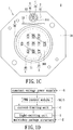
- the first embodiment of the instant disclosure provides a multichip package structure Z using a constant voltage power supply S.
- the multichip package structure Z comprises a substrate unit 1, a light-emitting unit 2, a current-limiting unit C, a frame unit 3 and a package unit 4.
- the substrate unit 1 includes a substrate body 10 having a first chip-placing region 11 and a second chip-placing region 12 formed on the top surface of the substrate body 10.
- the substrate body 10 includes a circuit substrate 100, a heat-dissipating layer 101 disposed on the bottom surface of the circuit substrate 100, a plurality conductive pads 102 disposed on the top surface of the circuit substrate 100, and an insulative layer 103 disposed on the top surface of the circuit substrate 100 to expose the conductive pads 102.
- the heat-dissipating efficiency of the circuit substrate 100 is increased by using the heat-dissipating layer 101, and the insulative layer 103 is a solder mask for only exposing the conductive pads 102 in order to achieve local soldering.
- the substrate body 10 can be a PCB (Printed Circuit Board), a flexible substrate, an aluminum substrate, a ceramic substrate, or a copper substrate.
- the light-emitting unit 2 includes a plurality of light-emitting chips (bare die state) 20 electrically connected to and disposed on the first chip-placing region 11.
- each light-emitting chip 20 may be an LED (Light-emitting diode) such as a blue LED, and each light-emitting chip 20 can be electrically connected to the first chip-placing region 11 by wire bonding.
- designer can plan a predetermined first chip-placing region 11 on the substrate body 10 in advance, thus the first light-emitting chips 20 can be placed on the first chip-placing region 11.
- the current-limiting unit C includes at least one current-limiting chip C1 electrically connected to and disposed on the second chip-placing region 12, and the current-limiting chip C1 is electrically connected to the light-emitting unit 2.
- the current-limiting unit C can also include a plurality of current-limiting chips C1 on the second chip-placing region 12 for different requirements of amperage or current.
- the current-limiting chip C1 can be electrically connected to the second chip-placing region 12 by wire bonding and electrically connected between the constant voltage power supply S and the light-emitting unit 2 (as shown in FIG. 1D ).
- the instant disclosure further comprises a control unit 5 that includes at least one PWM (Pulse Width Modulation) control module 50 selectively electrically connected to the current-limiting chip C1, thus the current-limiting unit C can be electrically connected between the control unit 5 and the light-emitting unit 2.
- PWM Pulse Width Modulation
- control unit 5 also can be omitted from the instant disclosure.
- the PWM control module 50 can control the light-emitting chip 20 to generate a predetermined pulse frequency, such as 50Hz, 60Hz, ..., 120Hz, etc.
- the frame unit 3 includes a first surrounding colloid frame 30 and a second surrounding colloid frame 31 surroundingly formed on the top surface of the substrate body 10 by coating or other forming method.
- the first surrounding colloid frame 30 surrounds the light-emitting chips 20 to form a first colloid position limiting space 300 corresponding to the first chip-placing region 11, and the second surrounding colloid frame 31 surrounds the current-limiting chip C1 to form a second colloid position limiting space 310 corresponding to the second chip-placing region 12.
- the first surrounding colloid frame 30 and the second surrounding colloid frame 31 are separated from each other by a predetermined distance.
- the method for forming the first surrounding colloid frame 30 includes: first, surroundingly coating liquid colloid (not shown) on the top surface of the substrate body 10.
- the liquid colloid can be coated on the substrate body 10 to form any shapes according to different requirements (such as a circular shape, a square or a rectangular shape etc.).
- the thixotropic index of the liquid colloid may be between 4 and 6
- the pressure of coating the liquid colloid on the top surface of the substrate body 10 may be between 350 kpa and 450 kpa
- the velocity of coating the liquid colloid on the top surface of the substrate body 10 may be between 5 mm/s and 15 mm/s.
- the liquid colloid is surroundingly coated on the top surface of the substrate body 10 from a start point to a termination point, and the position of the start point and the position of the termination point are substantially the same, thus the first surrounding colloid frame 30 (or the second surrounding colloid frame 31) has a micro convex portion close to the start point and the termination point.
- the method further includes: hardening or curing the liquid colloid to form a first surrounding colloid frame 30.
- the liquid colloid is hardened by baking, the baking temperature may be between 120°C and 140°C, and the baking time may be between 20 minute and 40 minute.
- the first surrounding colloid frame 30 has an arc shape formed on the top surface thereof, the first surrounding colloid frame 30 has a radius tangent T and the angle ⁇ of the radius tangent T relative to the top surface of the substrate body 10 may be between 40° and 50°, the maximum height H of the first surrounding colloid frame 30 relative to the top surface of the substrate body 10 may be between 0.3 mm and 0.7 mm, the width D of the bottom side of the first surrounding colloid frame 30 may be between 1.5 mm and 3 mm, the thixotropic index of the first surrounding colloid frame 30 may be between 4 and 6, and the first surrounding colloid frame 30 is formed by mixing inorganic additive with white thermohardening colloid.
- the package unit 4 includes a first package colloid body 40 filled into the first colloid position limiting space 300 to cover the light-emitting chips 20 and a second package colloid body 41 filled into the second colloid position limiting space 310 to cover the current-limiting chip C1.
- the first package colloid body 40 and the second package colloid body 41 are separated from each other by a predetermined distance, and the first surrounding colloid frame 30 and the second package colloid body 41 are separated from each other by a predetermined distance.
- the first package colloid body 40 may be a light-permitting colloid body such as cured phosphor colloid or cured transparent colloid, thus blue light beams L1 generated by the light-emitting chips 20 (the blue LED chips) can pass through the first package colloid body 40 (the cured phosphor colloid) to generate white light beams L2 that are similar to the light source generate by sun lamp.
- the second package colloid body 41 may be a cured opaque colloid covering the current-limiting chip C1, thus the second package colloid body 41 can prevent the current-limiting chip C1 from being damaged or affected by lighting of the white light beams L2.
- the substrate unit 1 further includes at least one heat-insulating slot 13 passing through the substrate body 10, and the heat-insulating slot 13 is formed between the light-emitting unit 2 and the current-limiting unit C or between the first surrounding colloid frame 30 and the second surrounding colloid frame 31.
- the heat-transmitting path between the light-emitting unit 2 and the current-limiting unit C can be effectively reduced by using the heat-insulating slot 13, thus the velocity of transmitting the heat generated by the current-limiting chip C1 to the light-emitting unit 2 can be effectively decreased.
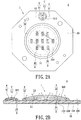
- the second embodiment of the instant disclosure provides a multichip package structure Z using a constant voltage power supply (not shown). Comparing FIG. 2A with FIG. 1A (or FIG. 2B with FIG. 1B ), the difference between the second embodiment and the first embodiment is that: the heat-insulating slot 13 shown in FIG. 2A can be omitted in the second embodiment. For example, when the heat generated by the current-limiting chip C1 is very small, the user can use the second embodiment.
- the third embodiment of the instant disclosure provides a multichip package structure Z using a constant voltage power supply (not shown).
- the difference between the third embodiment and the first embodiment is that: the current-limiting unit C is disposed between the first surrounding colloid frame 30 and the second surrounding colloid frame 31, the second surrounding colloid frame 31 surrounds the first surrounding colloid frame 30, the second package colloid body 41 surrounds the first package colloid body 40, and the first surrounding colloid frame 30 is connected with the second package colloid body 41.
- the first surrounding colloid frame 30 only surrounds the light-emitting chips 20
- the second surrounding colloid frame 31 simultaneously surrounds the light-emitting chips 20
- the first surrounding colloid frame 30 and the current-limiting chip C1 thus the first surrounding colloid frame 30 and the second surrounding colloid frame 31 are arranged to form a concentric circle.
- the substrate unit 1 further includes at least one heat-insulating slot 13 passing through the substrate body 10, and the heat-insulating slot 13 is formed between the light-emitting unit 2 and the current-limiting unit C or between the first surrounding colloid frame 30 and the second surrounding colloid frame 31.
- the heat-transmitting path between the light-emitting unit 2 and the current-limiting unit C can be effectively reduced by using the heat-insulating slot 13, thus the velocity of transmitting the heat generated by the current-limiting chip C1 to the light-emitting unit 2 can be effectively decreased.
- the heat-insulating slot 13 shown in FIG. 3 can be omitted.
- the fourth embodiment of the instant disclosure provides a multichip package structure Z using a constant voltage power supply (not shown).
- the multichip package structure Z comprises a substrate unit 1, a light-emitting unit 2, a current-limiting unit C, a frame unit 3 and a package unit 4.
- the substrate unit 1 includes a substrate body 10 having two first chip-placing regions 11 and a second chip-placing region 12 formed on the top surface of the substrate body 10.
- the substrate body 10 includes a circuit substrate 100, a heat-dissipating layer 101 disposed on the bottom surface of the circuit substrate 100, a plurality conductive pads 102 disposed on the top surface of the circuit substrate 100, and an insulative layer 103 disposed on the top surface of the circuit substrate 100 to expose the conductive pads 102.
- the light-emitting unit 2 includes at least one first light-emitting module 2a for generating first color temperature and at least one second light-emitting module 2b for generating second color temperature.
- the first light-emitting module 2a includes a plurality of first light-emitting chips 20a electrically connected to and disposed on one of the first chip-placing regions 11, and the second light-emitting module 2b includes a plurality of second light-emitting chips 20b electrically connected to and disposed on the other first chip-placing region 11.
- each first light-emitting chip 20a and each second light-emitting chip 20b may be a blue LED, and each first light-emitting chip 20a and each second light-emitting chip 20b can be respectively and electrically connected to the two first chip-placing regions 11 by wire bonding.
- the current-limiting unit C includes at least one current-limiting chip C1 electrically connected to and disposed on the second chip-placing region 12, and the current-limiting chip C1 is electrically connected to the light-emitting unit 2.
- the current-limiting unit C can also include a plurality of current-limiting chips C1 on the second chip-placing region 12 for different requirements of amperage or current.
- the current-limiting chip C1 can be electrically connected to the second chip-placing region 12 by wire bonding and electrically connected between the constant voltage power supply (not shown) and the light-emitting unit 2.
- the current-limiting chip C1 is electrically connected between the constant voltage power supply (not shown) and the light-emitting unit 2, thus the light-emitting unit 2 can obtain constant voltage from the constant voltage power supply (not shown) through the current-limiting chip C1.
- the frame unit 3 includes two first surrounding colloid frames 30 and a second surrounding colloid frame 31 surroundingly formed on the top surface of the substrate body 10 by coating or other forming method.
- the two first surrounding colloid frames 30 respectively surround the first light-emitting module 2a and the second light-emitting module 2b to respectively form two first colloid position limiting spaces 300 corresponding to the two first chip-placing regions 11, and the second surrounding colloid frame 31 surrounds the current-limiting chip C1 to form a second colloid position limiting space 310 corresponding to the second chip-placing region 12.
- the two first surrounding colloid frames 30 are separated from each other and arranged on the substrate body 10 in parallel, and each first surrounding colloid frame 30 and the second surrounding colloid frame 31 are separated from each other.
- the package unit 4 includes two first package colloid bodies (40a, 40b) and a second package colloid body 41.
- the two first package colloid bodies (40a, 40b) are respectively filled into the two first colloid position limiting spaces 300 to respectively cover the first light-emitting module 2a and the second light-emitting module 2b, and the second package colloid body 41 is filled into the second colloid position limiting space 310 to cover the current-limiting chip C1.
- Each first package colloid bodies (40a, 40b) and the second package colloid body 41 are separated from each other, and each first surrounding colloid frame 30 and the second package colloid body 41 are separated from each other.
- one first package colloid body 40a may be a cured phosphor colloid with first color
- the other first package colloid body 40b may be a cured phosphor colloid with second color
- the second package colloid body 41 may be a cured opaque colloid.
- the substrate unit 1 further includes at least one heat-insulating slot 13 passing through the substrate body 10, and the heat-insulating slot 13 is formed between the light-emitting unit 2 and the current-limiting unit C or between one of the two first surrounding colloid frames 30 and the second surrounding colloid frame 31, thus the velocity of transmitting the heat generated by the current-limiting chip C1 to the light-emitting unit 2 can be effectively decreased.
- the heat-insulating slot 13 can be omitted.
- the first light-emitting structure N1 may comprises the substrate body 10, the first light-emitting chips 20a, one first surrounding colloid frame 30 and one first package colloid body 40a.
- the second light-emitting structure N2 may comprises the substrate body 10, the second light-emitting chips 20b, the other first surrounding colloid frame 30 and the other first package colloid body 40b.
- the fifth embodiment of the instant disclosure provides a multichip package structure Z using a constant voltage power supply (not shown). Comparing FIG. 5A with FIG. 4A (or FIG. 5B with FIG. 4B ), the difference between the fifth embodiment and the fourth embodiment is that: in the fifth embodiment, the two first surrounding colloid frames 30 can be arranged on the substrate body 10 in series.
- each first surrounding colloid frame 30 may be a cured phosphor colloid.
- phosphor powders can be selectively add to each first surrounding colloid frame 30 according to different requirements, thus dark bands generated between the two first package colloid bodies (40a, 40b) can be effectively decreased or eliminated.
- the seventh embodiment of the instant disclosure provides a multichip package structure Z using a constant voltage power supply (not shown).
- the multichip package structure Z comprises a substrate unit 1, a light-emitting unit 2, a current-limiting unit C, a frame unit 3 and a package unit 4.
- the substrate unit 1 includes a substrate body 10 having two first chip-placing regions 11 and a second chip-placing region 12 formed on the top surface of the substrate body 10.
- the light-emitting unit 2 includes at least one first light-emitting module 2a for generating first color temperature and at least one second light-emitting module 2b for generating second color temperature.
- the first light-emitting module 2a includes a plurality of first light-emitting chips 20a electrically connected to and disposed on one of the first chip-placing regions 11, and the second light-emitting module 2b includes a plurality of second light-emitting chips 20b electrically connected to and disposed on the other first chip-placing region 11.
- the current-limiting unit C includes at least one current-limiting chip C1 electrically connected to and disposed on the second chip-placing region 12, and the current-limiting chip C1 is electrically connected to the light-emitting unit 2.
- the frame unit 3 includes two first surrounding colloid frames (30a, 30b) and a second surrounding colloid frame 31 surroundingly formed on the top surface of the substrate body 10 by coating or other forming method.
- One first surrounding colloid frame 30b surrounds the other first surrounding colloid frame 30a, thus the two first surrounding colloid frames (30a, 30b) are arranged to form a concentric circle.
- the two first surrounding colloid frames (30a, 30b) respectively surround the first light-emitting module 2a and the second light-emitting module 2b to respectively form two first colloid position limiting spaces 300 corresponding to the two first chip-placing regions 11, the second light-emitting module 2b is disposed between the two first surrounding colloid frames (30a, 30b), and the second surrounding colloid frame 31 surrounds the current-limiting chip C1 to form a second colloid position limiting space 310 corresponding to the second chip-placing region 12.
- the package unit 4 includes two first package colloid bodies (40a, 40b) and a second package colloid body 41.
- the two first package colloid bodies (40a, 40b) are respectively filled into the two first colloid position limiting spaces 300 to respectively cover the first light-emitting module 2a and the second light-emitting module 2b, and the second package colloid body 41 is filled into the second colloid position limiting space 310 to cover the current-limiting chip C1.
- the substrate unit 1 further includes at least one heat-insulating slot 13 passing through the substrate body 10, and the heat-insulating slot 13 is formed between the light-emitting unit 2 and the current-limiting unit C or between one of the two first surrounding colloid frames 30b and the second surrounding colloid frame 31, thus the velocity of transmitting the heat generated by the current-limiting chip C1 to the light-emitting unit 2 can be effectively decreased.
- the heat-insulating slot 13 can be omitted.
- the first light-emitting structure N1 may comprises the substrate body 10, the first light-emitting chips 20a, one first surrounding colloid frame 30a and one first package colloid body 40a.
- the second light-emitting structure N2 may comprises the substrate body 10, the second light-emitting chips 20b, the other first surrounding colloid frame 30b and the other first package colloid body 40b.
- the second light-emitting structure N2 with high color temperature can be an outer ring to surround the first light-emitting structure N1 with low color temperature.
- the eighth embodiment of the instant disclosure provides a multichip package structure Z using a constant voltage power supply (not shown). Comparing FIG. 8 with FIG. 7A , the difference between the eighth embodiment and the seventh embodiment is that: in the eighth embodiment, the first light-emitting structure N1 with low color temperature can be an outer ring to surround the second light-emitting structure N2 with high color temperature.
- each first surrounding colloid frame (30a, 30b) may be a cured phosphor colloid.
- phosphor powders can be selectively add to each first surrounding colloid frame (30a, 30b) according to different requirements, thus dark bands generated between the two first package colloid bodies (40a, 40b) can be effectively decreased or eliminated.
- the tenth embodiment of the instant disclosure provides a multichip package structure Z using a constant voltage power supply (not shown).
- the difference between the tenth embodiment and the seventh embodiment is that: in the tenth embodiment, the inner first surrounding colloid frame 30a may be a cured phosphor colloid and the outer first surrounding colloid frame 30b may be a cured light-reflecting colloid.
- phosphor powders can be selectively add to the inner first surrounding colloid frame 30a according to different requirements, thus light beams generated by the light-emitting unit 2 can be transmitted into the inner first surrounding colloid frame 30a for effectively decreasing or eliminating dark bands generated between the two first package colloid bodies (40a, 40b).
- light beams generated by the light-emitting unit 2 can be effectively reflected or condensed by the outer first surrounding colloid frame 30b.
- the substrate unit 1 includes a plurality of positive pads P and negative pads N disposed on the top surface of the substrate body 10.
- Each light-emitting chip (20 or 20a, 20b) has a positive electrode 201 and a negative electrode 202.
- the positive electrode 201 of each light-emitting chip 20 corresponds to at least two of the positive pads P
- the negative electrode 202 of each light-emitting chip 20 corresponds to at least two of the negative pads N.
- the multichip package structure further comprises a conductive wire unit W including a plurality of conductive wires W1.
- Every two conductive wires W1 are respectively electrically connected between the positive electrode 201 of each light-emitting chip 20 and one of the at least two positive pads P and between the negative electrode 202 of each light-emitting chip 20 and one of the at least two negative pads N.
- the positive electrode 201 of each light-emitting chip 20 has at least one standby positive pad P and the negative electrode 202 of each light-emitting chip 20 has at least one standby negative pad N.
- the manufacturer can make the same first end of the conductive wire W1 connect to another one of the at least two positive pads P or the at least two negative pads N without cleaning solder splash on the surface of the first one of the at least two positive pads P or the at least two negative pads N, thus the wire-bonding time (the wire-bonding efficiency) can be decreased and the wire-bonding yield can be increased.
- the first surrounding colloid frame (such as a surrounding white colloid frame) of any shapes can be formed by coating in the instant disclosure.
- the position of the first package colloid body such as cured phosphor colloid can be limited in the first colloid position limiting space by using the first surrounding colloid frame, and the shape of the first package colloid body can be adjusted by using the first surrounding colloid frame. Therefore, the instant disclosure can increase the light-emitting efficiency of the light-emitting chips and control the light-projecting angle of the light-emitting chips.
- the first package colloid body is limited in the first colloid position limiting space by using the first surrounding colloid frame, thus the usage quantity of the first package colloid body can be controlled by the manufacture.
- the surface shape and the height of the first package colloid body can be adjusted by controlling the usage quantity of the first package colloid body, thus the light-projecting angles of the white light beams can be adjusted.
- the blue light beams generated by the light-emitting chips can be reflected by an inner wall of the first surrounding colloid frame, thus the light-emitting efficiency of the instant disclosure can be effectively increased.
- the positive electrode and the negative electrode of each light-emitting chip respectively correspond to at least two of the positive pads and at least two of the negative pads, thus the positive electrode of each light-emitting chip has at least one standby positive pad and the negative electrode of each light-emitting chip has at least one standby negative pad.
- the light-emitting chips and the at least one current-limiting chip are electrically connected to the same substrate body, thus the multichip package structure can use the constant voltage power supply as power supply source.
Claims (6)
- Structure de boîtier à plusieurs puces (Z), comprenant :une unité substrat (1) qui comprend un corps de substrat (10) qui présente deux premières régions de placement de puce (11), et une seconde région de placement de puce (12) formée sur la surface supérieure du corps de substrat (10) ;une unité électroluminescente (2) qui comprend au moins un premier module électroluminescent (2a) destiné à générer une première température de couleur, et au moins un second module électroluminescent (2b) destiné à générer une seconde température de couleur différente de la première température de couleur ;dans laquelle le premier module électroluminescent (2a) comprend une pluralité de premières puces électroluminescentes (20a) connectées de manière électrique à l'une des premières régions de placement de puce (11), et disposées sur celle-ci, et le second module électroluminescent (2b) comprend une pluralité de secondes puces électroluminescentes (20b) connectées de manière électrique à l'autre première région de placement de puce (11) ;une unité de limitation du courant (C) qui comprend au moins une puce de limitation du courant (C1) connectée de manière électrique à la seconde région de placement de puce (12), et disposée sur celle-ci, dans laquelle la puce de limitation du courant (C1) est connectée de manière électrique à l'unité électroluminescente (2) ;une unité cadre (3) qui comprend deux premiers cadres colloïdaux environnants (30a, 30b) et un second cadre colloïdal environnant (31) formés de manière environnante sur la surface supérieure du corps de substrat (10) ; etune unité boîtier (4) qui comprend deux premiers corps colloïdaux de boîtier distincts (40a, 40b) et un second corps colloïdal de boîtier (41) ;dans laquelle l'un (30b) des premiers cadres colloïdaux environnants (30a, 30b) entoure l'autre premier cadre colloïdal environnant (30a), les deux premiers cadres colloïdaux environnants (30a, 30b) entourent respectivement le premier module électroluminescent (2a) et le second module électroluminescent (2b) de façon à former respectivement deux premiers espaces de limitation de la position colloïdale (300) qui correspondent aux deux premières régions de placement de puce (11), le second module électroluminescent (2b) est disposé entre les deux premiers cadres colloïdaux environnants (30a, 30b) ;dans laquelle la pluralité de secondes puces électroluminescentes (20b) entourent le premier module électroluminescent (2a), et le second cadre colloïdal environnant (31) entoure la puce de limitation du courant (C1) de façon à former un second espace de limitation de la position colloïdale (310) qui correspond à la seconde région de placement de puce (12), dans laquelle les deux premiers corps colloïdaux de boîtier (40a, 40b) sont respectivement placés dans les deux premiers espaces de limitation de la position colloïdale (300) de façon à couvrir respectivement le premier module électroluminescent (2a) et le second module électroluminescent (2b), et le second corps colloïdal de boîtier (41) est placé dans le second espace de limitation de la position colloïdale (310) de façon à enfermer la puce de limitation du courant (C1), dans laquelle les deux premiers cadres colloïdaux environnants (30a, 30b) et les deux premiers corps colloïdaux de boîtier (40a, 40b) sont connectés de manière alternée les uns aux autres.
- Structure de boîtier à plusieurs puces (Z) selon la revendication 1, dans laquelle le corps de substrat (10) comprend un substrat de circuit (100), une couche de dissipation de la chaleur (101) disposée sur la surface inférieure du substrat de circuit (100), une pluralité de plages conductrices (102) disposées sur la surface supérieure du substrat de circuit (100), et une couche isolante (103) disposée sur la surface supérieure du substrat de circuit (100) de façon à exposer les plages conductrices (102), dans laquelle chaque puce électroluminescente (20) est une LED bleue, le premier corps colloïdal de boîtier (40) est du phosphore colloïdal durci ou un colloïde transparent durci, et le second corps colloïdal de boîtier (41) est un colloïde opaque durci.
- Structure de boîtier à plusieurs puces (Z) selon la revendication 1, dans laquelle l'unité substrat (1) comprend une pluralité de plages positives (P) et de plages négatives (N) disposées sur la surface supérieure du corps de substrat (10), chaque puce électroluminescente (20) présente une électrode positive (201) et une électrode négative (202), l'électrode positive (201) de chaque puce électroluminescente (20) correspond à deux au moins des plages positives (P), et l'électrode négative (202) de chaque puce électroluminescente (20) correspond à deux au moins des plages négatives (N).
- Structure de boîtier à plusieurs puces (Z) selon la revendication 3, comprenant en outre : une unité fil conducteur (W) qui comprend une pluralité de fils conducteurs (W1), dans laquelle les fils conducteurs (W1) sont respectivement connectés de manière électrique deux à deux entre l'électrode positive (201) de chaque puce électroluminescente (20) et l'une des deux plages positives (P) au moins, et entre l'électrode négative (202) de chaque puce électroluminescente (20) et l'une des deux plages négatives (N) au moins.
- Structure de boîtier à plusieurs puces (Z) selon la revendication 1, dans laquelle l'unité substrat (1) comprend au moins une fente d'isolation thermique (13) qui passe à travers le corps de substrat (10), et la fente d'isolation thermique (13) est formée entre l'unité électroluminescente (2) et l'unité de limitation du courant (C), ou entre le premier cadre colloïdal environnant (30a) et le second cadre colloïdal environnant (31).
- Structure de boîtier à plusieurs puces (Z) selon la revendication 1, comprenant en outre une unité de commande (5) qui comprend au moins un module de commande PWM (50) connecté de manière électrique à la ou aux puces de limitation du courant (C1), dans laquelle l'unité de limitation du courant (C) est connectée de manière électrique entre l'unité de commande (5) et l'unité électroluminescente (2).
Applications Claiming Priority (1)
| Application Number | Priority Date | Filing Date | Title |
|---|---|---|---|
| TW099136124A TWI419373B (zh) | 2010-10-22 | 2010-10-22 | 使用定電壓電源供應器之多晶封裝結構 |
Publications (3)
| Publication Number | Publication Date |
|---|---|
| EP2445007A2 EP2445007A2 (fr) | 2012-04-25 |
| EP2445007A3 EP2445007A3 (fr) | 2013-12-25 |
| EP2445007B1 true EP2445007B1 (fr) | 2017-07-26 |
Family
ID=44789365
Family Applications (1)
| Application Number | Title | Priority Date | Filing Date |
|---|---|---|---|
| EP11185564.9A Active EP2445007B1 (fr) | 2010-10-22 | 2011-10-18 | Structure de boîtier à plusieurs puces utilisant une alimentation électrique à tension constante |
Country Status (4)
| Country | Link |
|---|---|
| US (1) | US8405118B2 (fr) |
| EP (1) | EP2445007B1 (fr) |
| JP (1) | JP2012094865A (fr) |
| TW (1) | TWI419373B (fr) |
Families Citing this family (24)
| Publication number | Priority date | Publication date | Assignee | Title |
|---|---|---|---|---|
| TWI408794B (zh) * | 2011-01-26 | 2013-09-11 | Paragon Sc Lighting Tech Co | 混光式多晶封裝結構 |
| JP5582048B2 (ja) * | 2011-01-28 | 2014-09-03 | 日亜化学工業株式会社 | 発光装置 |
| TWM410983U (en) * | 2011-04-22 | 2011-09-01 | Paragon Sc Lighting Tech Co | Light emitting module |
| TWM422032U (en) * | 2011-10-11 | 2012-02-01 | Paragon Sc Lighting Tech Co | LED lamp module |
| TWI584671B (zh) * | 2012-03-28 | 2017-05-21 | 艾笛森光電股份有限公司 | 燈具及其發光二極體模組 |
| JP6072472B2 (ja) | 2012-08-27 | 2017-02-01 | シチズン電子株式会社 | Led発光装置 |
| KR101957701B1 (ko) * | 2012-11-14 | 2019-03-14 | 삼성전자주식회사 | 발광소자 패키지 및 그 제조방법 |
| JP5979494B2 (ja) * | 2012-12-20 | 2016-08-24 | パナソニックIpマネジメント株式会社 | 照明装置及び発光モジュール |
| JP6068175B2 (ja) * | 2013-02-12 | 2017-01-25 | 新光電気工業株式会社 | 配線基板、発光装置、配線基板の製造方法及び発光装置の製造方法 |
| CN103196049A (zh) * | 2013-03-06 | 2013-07-10 | 深圳市晶台光电有限公司 | 一种采用一体化cob封装工艺的led灯板 |
| KR102085888B1 (ko) * | 2013-05-08 | 2020-03-06 | 엘지이노텍 주식회사 | 발광 소자 |
| TWI518955B (zh) * | 2013-08-30 | 2016-01-21 | 柏友照明科技股份有限公司 | 多晶片封裝結構 |
| CN106465532A (zh) * | 2014-05-22 | 2017-02-22 | 三菱电机株式会社 | 电动机用控制装置 |
| JP6201904B2 (ja) * | 2014-06-10 | 2017-09-27 | 豊田合成株式会社 | 発光装置 |
| USD751517S1 (en) | 2014-06-16 | 2016-03-15 | Citizen Electronics Co., Ltd. | Light emitting diode |
| USD751045S1 (en) | 2014-06-16 | 2016-03-08 | Citizen Electronics Co., Ltd. | Light emitting diode |
| USD751046S1 (en) | 2014-06-16 | 2016-03-08 | Citizen Electronics Co., Ltd. | Light emitting diode |
| JP6341804B2 (ja) * | 2014-08-22 | 2018-06-13 | コイト電工株式会社 | 放熱構造 |
| JP6372257B2 (ja) * | 2014-08-29 | 2018-08-15 | 東芝ライテック株式会社 | 車両用発光モジュール、車両用照明装置、および車両用灯具 |
| US10453825B2 (en) * | 2014-11-11 | 2019-10-22 | Cree, Inc. | Light emitting diode (LED) components and methods |
| JP6418908B2 (ja) * | 2014-11-11 | 2018-11-07 | シチズン電子株式会社 | Led発光装置 |
| CN106322174A (zh) * | 2015-06-24 | 2017-01-11 | 宏力照明集团有限公司 | 一种高性能led光电引擎模块 |
| DE102016219995A1 (de) * | 2016-10-13 | 2018-04-19 | Robert Bosch Gmbh | Elektronische Baugruppe und Verfahren zum Herstellen einer elektronischen Baugruppe |
| US10957736B2 (en) | 2018-03-12 | 2021-03-23 | Cree, Inc. | Light emitting diode (LED) components and methods |
Family Cites Families (15)
| Publication number | Priority date | Publication date | Assignee | Title |
|---|---|---|---|---|
| DE3146328A1 (de) * | 1981-11-23 | 1983-06-01 | Siemens AG, 1000 Berlin und 8000 München | Leuchtdiodenvorrichtung mit schutzeinrichtung zur begrenzung des durchlassstroms |
| JPH0677540A (ja) * | 1992-08-24 | 1994-03-18 | Sanyo Electric Co Ltd | 光半導体装置 |
| JP2001272938A (ja) * | 2000-03-28 | 2001-10-05 | Sharp Corp | 色調調整回路およびその回路を備えたバックライトモジュールおよび発光ダイオード表示装置 |
| TWI329368B (en) * | 2004-11-15 | 2010-08-21 | Chunghwa Picture Tubes Ltd | White light led |
| US7586125B2 (en) * | 2006-02-20 | 2009-09-08 | Industrial Technology Research Institute | Light emitting diode package structure and fabricating method thereof |
| KR101318968B1 (ko) * | 2006-06-28 | 2013-10-17 | 서울반도체 주식회사 | 발광 다이오드를 이용한 인공태양광 시스템 |
| JP5172500B2 (ja) * | 2007-07-27 | 2013-03-27 | ローム株式会社 | 駆動装置 |
| JP5106049B2 (ja) * | 2007-11-02 | 2012-12-26 | シャープ株式会社 | 照明装置及び照明システム |
| JP2009140718A (ja) * | 2007-12-05 | 2009-06-25 | Toshiba Lighting & Technology Corp | 照明装置 |
| JP5056520B2 (ja) * | 2008-03-21 | 2012-10-24 | 東芝ライテック株式会社 | 照明装置 |
| JP5169858B2 (ja) * | 2009-01-16 | 2013-03-27 | 株式会社デンソー | 車両用led駆動装置 |
| TWI411143B (en) * | 2009-06-26 | 2013-10-01 | Led package structure with a plurality of standby pads for increasing wire-bonding yield and method for manufacturing the same | |
| TWM368194U (en) * | 2009-06-26 | 2009-11-01 | Numen Technology Inc | Packaging structure of light emitting elements |
| US8547023B2 (en) * | 2010-06-28 | 2013-10-01 | Rui Teng Opto Technology Co., Ltd. | LED light source module |
| TWI442540B (zh) * | 2010-10-22 | 2014-06-21 | Paragon Sc Lighting Tech Co | 直接電性連接於交流電源之多晶封裝結構 |
-
2010
- 2010-10-22 TW TW099136124A patent/TWI419373B/zh active
- 2010-12-27 US US12/979,201 patent/US8405118B2/en active Active
-
2011
- 2011-10-18 EP EP11185564.9A patent/EP2445007B1/fr active Active
- 2011-10-20 JP JP2011230678A patent/JP2012094865A/ja active Pending
Non-Patent Citations (1)
| Title |
|---|
| None * |
Also Published As
| Publication number | Publication date |
|---|---|
| EP2445007A3 (fr) | 2013-12-25 |
| US20120097997A1 (en) | 2012-04-26 |
| US8405118B2 (en) | 2013-03-26 |
| TW201218430A (en) | 2012-05-01 |
| TWI419373B (zh) | 2013-12-11 |
| EP2445007A2 (fr) | 2012-04-25 |
| JP2012094865A (ja) | 2012-05-17 |
Similar Documents
| Publication | Publication Date | Title |
|---|---|---|
| EP2445007B1 (fr) | Structure de boîtier à plusieurs puces utilisant une alimentation électrique à tension constante | |
| US9078312B2 (en) | Multichip package structure for directly electrically connecting to an AC power source | |
| US8421373B2 (en) | Light-mixing multichip package structure | |
| US8779660B2 (en) | Illumination device for enhancing plant growth | |
| US8672517B2 (en) | Light-emitting module | |
| EP2290279B1 (fr) | Structure de conditionnement DEL à mélange de lumière pour augmenter l'indice de rendu des couleurs et la luminosité | |
| US8187899B2 (en) | LED package structure for increasing light-emitting efficiency and controlling light-projecting angle and method for manufacturing the same | |
| JP2013219340A (ja) | 発光装置、並びにそれを用いた照明装置及び照明器具 | |
| US8820960B2 (en) | Light emitting device | |
| US8899789B2 (en) | Lamp module | |
| WO2013136389A1 (fr) | Substrat, dispositif électroluminescent et dispositif d'éclairage | |
| US20110044039A1 (en) | Led lamp construction with integral appearance | |
| US9780274B2 (en) | Light-emitting apparatus and illumination apparatus | |
| US20110101389A1 (en) | Multichip type led package structure for generating light-emitting effect similar to circle shape by single wire or dual wire bonding method alternatively | |
| CN104976547A (zh) | 发光二极管组件及用此发光二极管组件的发光二极管灯泡 | |
| US10490721B2 (en) | Light-emitting device and illuminating apparatus | |
| JP6277510B2 (ja) | 発光モジュール、照明装置および照明器具 | |
| JP6076796B2 (ja) | 半導体発光装置 | |
| US8876334B2 (en) | Light-mixing multichip package structure | |
| JP2009176923A (ja) | 光電子素子 | |
| TWM524431U (zh) | 發光模組及其燈具 | |
| JP5216948B1 (ja) | 基板、発光装置及び照明装置 | |
| JP2018010800A (ja) | 発光装置、及び、照明用光源 | |
| KR20170000502A (ko) | 광원 모듈 | |
| KR101694178B1 (ko) | 발광 소자 |
Legal Events
| Date | Code | Title | Description |
|---|---|---|---|
| AK | Designated contracting states |
Kind code of ref document: A2 Designated state(s): AL AT BE BG CH CY CZ DE DK EE ES FI FR GB GR HR HU IE IS IT LI LT LU LV MC MK MT NL NO PL PT RO RS SE SI SK SM TR |
|
| AX | Request for extension of the european patent |
Extension state: BA ME |
|
| PUAI | Public reference made under article 153(3) epc to a published international application that has entered the european phase |
Free format text: ORIGINAL CODE: 0009012 |
|
| RIC1 | Information provided on ipc code assigned before grant |
Ipc: H01L 33/62 20100101ALN20130820BHEP Ipc: F21K 99/00 20100101ALN20130820BHEP Ipc: H01L 33/48 20100101ALI20130820BHEP Ipc: H01L 25/16 20060101AFI20130820BHEP Ipc: H01L 33/52 20100101ALN20130820BHEP |
|
| PUAL | Search report despatched |
Free format text: ORIGINAL CODE: 0009013 |
|
| AK | Designated contracting states |
Kind code of ref document: A3 Designated state(s): AL AT BE BG CH CY CZ DE DK EE ES FI FR GB GR HR HU IE IS IT LI LT LU LV MC MK MT NL NO PL PT RO RS SE SI SK SM TR |
|
| AX | Request for extension of the european patent |
Extension state: BA ME |
|
| RIC1 | Information provided on ipc code assigned before grant |
Ipc: F21V 15/06 20060101ALI20131118BHEP Ipc: H01L 33/62 20100101ALN20131118BHEP Ipc: F21V 23/00 20060101ALN20131118BHEP Ipc: H01L 25/16 20060101AFI20131118BHEP Ipc: H01L 33/52 20100101ALN20131118BHEP Ipc: H01L 33/48 20100101ALI20131118BHEP |
|
| 17P | Request for examination filed |
Effective date: 20140325 |
|
| RBV | Designated contracting states (corrected) |
Designated state(s): AL AT BE BG CH CY CZ DE DK EE ES FI FR GB GR HR HU IE IS IT LI LT LU LV MC MK MT NL NO PL PT RO RS SE SI SK SM TR |
|
| GRAJ | Information related to disapproval of communication of intention to grant by the applicant or resumption of examination proceedings by the epo deleted |
Free format text: ORIGINAL CODE: EPIDOSDIGR1 |
|
| GRAP | Despatch of communication of intention to grant a patent |
Free format text: ORIGINAL CODE: EPIDOSNIGR1 |
|
| RIC1 | Information provided on ipc code assigned before grant |
Ipc: H01L 33/62 20100101ALN20170210BHEP Ipc: F21V 23/00 20150101ALN20170210BHEP Ipc: H01L 33/48 20100101ALI20170210BHEP Ipc: F21Y 105/10 20160101ALN20170210BHEP Ipc: H05K 1/02 20060101ALN20170210BHEP Ipc: F21Y 113/13 20160101ALN20170210BHEP Ipc: H01L 25/16 20060101AFI20170210BHEP Ipc: F21Y 115/10 20160101ALN20170210BHEP Ipc: H01L 33/52 20100101ALN20170210BHEP |
|
| INTG | Intention to grant announced |
Effective date: 20170310 |
|
| RIC1 | Information provided on ipc code assigned before grant |
Ipc: H05K 1/02 20060101ALN20170227BHEP Ipc: H01L 33/48 20100101ALI20170227BHEP Ipc: H01L 33/62 20100101ALN20170227BHEP Ipc: F21Y 113/13 20160101ALN20170227BHEP Ipc: F21Y 105/10 20160101ALN20170227BHEP Ipc: H01L 33/52 20100101ALN20170227BHEP Ipc: F21Y 115/10 20160101ALN20170227BHEP Ipc: F21V 23/00 20150101ALN20170227BHEP Ipc: H01L 25/16 20060101AFI20170227BHEP |
|
| GRAS | Grant fee paid |
Free format text: ORIGINAL CODE: EPIDOSNIGR3 |
|
| GRAA | (expected) grant |
Free format text: ORIGINAL CODE: 0009210 |
|
| AK | Designated contracting states |
Kind code of ref document: B1 Designated state(s): AL AT BE BG CH CY CZ DE DK EE ES FI FR GB GR HR HU IE IS IT LI LT LU LV MC MK MT NL NO PL PT RO RS SE SI SK SM TR |
|
| REG | Reference to a national code |
Ref country code: GB Ref legal event code: FG4D |
|
| REG | Reference to a national code |
Ref country code: CH Ref legal event code: EP |
|
| REG | Reference to a national code |
Ref country code: AT Ref legal event code: REF Ref document number: 913041 Country of ref document: AT Kind code of ref document: T Effective date: 20170815 |
|
| REG | Reference to a national code |
Ref country code: IE Ref legal event code: FG4D |
|
| REG | Reference to a national code |
Ref country code: DE Ref legal event code: R096 Ref document number: 602011039885 Country of ref document: DE |
|
| REG | Reference to a national code |
Ref country code: FR Ref legal event code: PLFP Year of fee payment: 7 |
|
| REG | Reference to a national code |
Ref country code: NL Ref legal event code: MP Effective date: 20170726 |
|
| REG | Reference to a national code |
Ref country code: LT Ref legal event code: MG4D |
|
| REG | Reference to a national code |
Ref country code: AT Ref legal event code: MK05 Ref document number: 913041 Country of ref document: AT Kind code of ref document: T Effective date: 20170726 |
|
| PG25 | Lapsed in a contracting state [announced via postgrant information from national office to epo] |
Ref country code: SE Free format text: LAPSE BECAUSE OF FAILURE TO SUBMIT A TRANSLATION OF THE DESCRIPTION OR TO PAY THE FEE WITHIN THE PRESCRIBED TIME-LIMIT Effective date: 20170726 Ref country code: LT Free format text: LAPSE BECAUSE OF FAILURE TO SUBMIT A TRANSLATION OF THE DESCRIPTION OR TO PAY THE FEE WITHIN THE PRESCRIBED TIME-LIMIT Effective date: 20170726 Ref country code: NL Free format text: LAPSE BECAUSE OF FAILURE TO SUBMIT A TRANSLATION OF THE DESCRIPTION OR TO PAY THE FEE WITHIN THE PRESCRIBED TIME-LIMIT Effective date: 20170726 Ref country code: HR Free format text: LAPSE BECAUSE OF FAILURE TO SUBMIT A TRANSLATION OF THE DESCRIPTION OR TO PAY THE FEE WITHIN THE PRESCRIBED TIME-LIMIT Effective date: 20170726 Ref country code: AT Free format text: LAPSE BECAUSE OF FAILURE TO SUBMIT A TRANSLATION OF THE DESCRIPTION OR TO PAY THE FEE WITHIN THE PRESCRIBED TIME-LIMIT Effective date: 20170726 Ref country code: NO Free format text: LAPSE BECAUSE OF FAILURE TO SUBMIT A TRANSLATION OF THE DESCRIPTION OR TO PAY THE FEE WITHIN THE PRESCRIBED TIME-LIMIT Effective date: 20171026 Ref country code: FI Free format text: LAPSE BECAUSE OF FAILURE TO SUBMIT A TRANSLATION OF THE DESCRIPTION OR TO PAY THE FEE WITHIN THE PRESCRIBED TIME-LIMIT Effective date: 20170726 |
|
| PG25 | Lapsed in a contracting state [announced via postgrant information from national office to epo] |
Ref country code: GR Free format text: LAPSE BECAUSE OF FAILURE TO SUBMIT A TRANSLATION OF THE DESCRIPTION OR TO PAY THE FEE WITHIN THE PRESCRIBED TIME-LIMIT Effective date: 20171027 Ref country code: IS Free format text: LAPSE BECAUSE OF FAILURE TO SUBMIT A TRANSLATION OF THE DESCRIPTION OR TO PAY THE FEE WITHIN THE PRESCRIBED TIME-LIMIT Effective date: 20171126 Ref country code: RS Free format text: LAPSE BECAUSE OF FAILURE TO SUBMIT A TRANSLATION OF THE DESCRIPTION OR TO PAY THE FEE WITHIN THE PRESCRIBED TIME-LIMIT Effective date: 20170726 Ref country code: ES Free format text: LAPSE BECAUSE OF FAILURE TO SUBMIT A TRANSLATION OF THE DESCRIPTION OR TO PAY THE FEE WITHIN THE PRESCRIBED TIME-LIMIT Effective date: 20170726 Ref country code: PL Free format text: LAPSE BECAUSE OF FAILURE TO SUBMIT A TRANSLATION OF THE DESCRIPTION OR TO PAY THE FEE WITHIN THE PRESCRIBED TIME-LIMIT Effective date: 20170726 Ref country code: BG Free format text: LAPSE BECAUSE OF FAILURE TO SUBMIT A TRANSLATION OF THE DESCRIPTION OR TO PAY THE FEE WITHIN THE PRESCRIBED TIME-LIMIT Effective date: 20171026 Ref country code: LV Free format text: LAPSE BECAUSE OF FAILURE TO SUBMIT A TRANSLATION OF THE DESCRIPTION OR TO PAY THE FEE WITHIN THE PRESCRIBED TIME-LIMIT Effective date: 20170726 |
|
| PG25 | Lapsed in a contracting state [announced via postgrant information from national office to epo] |
Ref country code: CZ Free format text: LAPSE BECAUSE OF FAILURE TO SUBMIT A TRANSLATION OF THE DESCRIPTION OR TO PAY THE FEE WITHIN THE PRESCRIBED TIME-LIMIT Effective date: 20170726 Ref country code: DK Free format text: LAPSE BECAUSE OF FAILURE TO SUBMIT A TRANSLATION OF THE DESCRIPTION OR TO PAY THE FEE WITHIN THE PRESCRIBED TIME-LIMIT Effective date: 20170726 Ref country code: RO Free format text: LAPSE BECAUSE OF FAILURE TO SUBMIT A TRANSLATION OF THE DESCRIPTION OR TO PAY THE FEE WITHIN THE PRESCRIBED TIME-LIMIT Effective date: 20170726 |
|
| REG | Reference to a national code |
Ref country code: DE Ref legal event code: R097 Ref document number: 602011039885 Country of ref document: DE |
|
| PG25 | Lapsed in a contracting state [announced via postgrant information from national office to epo] |
Ref country code: EE Free format text: LAPSE BECAUSE OF FAILURE TO SUBMIT A TRANSLATION OF THE DESCRIPTION OR TO PAY THE FEE WITHIN THE PRESCRIBED TIME-LIMIT Effective date: 20170726 Ref country code: MC Free format text: LAPSE BECAUSE OF FAILURE TO SUBMIT A TRANSLATION OF THE DESCRIPTION OR TO PAY THE FEE WITHIN THE PRESCRIBED TIME-LIMIT Effective date: 20170726 Ref country code: SK Free format text: LAPSE BECAUSE OF FAILURE TO SUBMIT A TRANSLATION OF THE DESCRIPTION OR TO PAY THE FEE WITHIN THE PRESCRIBED TIME-LIMIT Effective date: 20170726 Ref country code: SM Free format text: LAPSE BECAUSE OF FAILURE TO SUBMIT A TRANSLATION OF THE DESCRIPTION OR TO PAY THE FEE WITHIN THE PRESCRIBED TIME-LIMIT Effective date: 20170726 Ref country code: IT Free format text: LAPSE BECAUSE OF FAILURE TO SUBMIT A TRANSLATION OF THE DESCRIPTION OR TO PAY THE FEE WITHIN THE PRESCRIBED TIME-LIMIT Effective date: 20170726 |
|
| REG | Reference to a national code |
Ref country code: CH Ref legal event code: PL |
|
| PLBE | No opposition filed within time limit |
Free format text: ORIGINAL CODE: 0009261 |
|
| STAA | Information on the status of an ep patent application or granted ep patent |
Free format text: STATUS: NO OPPOSITION FILED WITHIN TIME LIMIT |
|
| 26N | No opposition filed |
Effective date: 20180430 |
|
| REG | Reference to a national code |
Ref country code: IE Ref legal event code: MM4A |
|
| PG25 | Lapsed in a contracting state [announced via postgrant information from national office to epo] |
Ref country code: LI Free format text: LAPSE BECAUSE OF NON-PAYMENT OF DUE FEES Effective date: 20171031 Ref country code: LU Free format text: LAPSE BECAUSE OF NON-PAYMENT OF DUE FEES Effective date: 20171018 Ref country code: CH Free format text: LAPSE BECAUSE OF NON-PAYMENT OF DUE FEES Effective date: 20171031 |
|
| REG | Reference to a national code |
Ref country code: BE Ref legal event code: MM Effective date: 20171031 |
|
| PG25 | Lapsed in a contracting state [announced via postgrant information from national office to epo] |
Ref country code: SI Free format text: LAPSE BECAUSE OF FAILURE TO SUBMIT A TRANSLATION OF THE DESCRIPTION OR TO PAY THE FEE WITHIN THE PRESCRIBED TIME-LIMIT Effective date: 20170726 Ref country code: BE Free format text: LAPSE BECAUSE OF NON-PAYMENT OF DUE FEES Effective date: 20171031 |
|
| PG25 | Lapsed in a contracting state [announced via postgrant information from national office to epo] |
Ref country code: MT Free format text: LAPSE BECAUSE OF NON-PAYMENT OF DUE FEES Effective date: 20171018 |
|
| REG | Reference to a national code |
Ref country code: FR Ref legal event code: PLFP Year of fee payment: 8 |
|
| PG25 | Lapsed in a contracting state [announced via postgrant information from national office to epo] |
Ref country code: IE Free format text: LAPSE BECAUSE OF NON-PAYMENT OF DUE FEES Effective date: 20171018 |
|
| PG25 | Lapsed in a contracting state [announced via postgrant information from national office to epo] |
Ref country code: HU Free format text: LAPSE BECAUSE OF FAILURE TO SUBMIT A TRANSLATION OF THE DESCRIPTION OR TO PAY THE FEE WITHIN THE PRESCRIBED TIME-LIMIT; INVALID AB INITIO Effective date: 20111018 |
|
| PG25 | Lapsed in a contracting state [announced via postgrant information from national office to epo] |
Ref country code: CY Free format text: LAPSE BECAUSE OF NON-PAYMENT OF DUE FEES Effective date: 20170726 |
|
| PG25 | Lapsed in a contracting state [announced via postgrant information from national office to epo] |
Ref country code: MK Free format text: LAPSE BECAUSE OF FAILURE TO SUBMIT A TRANSLATION OF THE DESCRIPTION OR TO PAY THE FEE WITHIN THE PRESCRIBED TIME-LIMIT Effective date: 20170726 |
|
| PG25 | Lapsed in a contracting state [announced via postgrant information from national office to epo] |
Ref country code: TR Free format text: LAPSE BECAUSE OF FAILURE TO SUBMIT A TRANSLATION OF THE DESCRIPTION OR TO PAY THE FEE WITHIN THE PRESCRIBED TIME-LIMIT Effective date: 20170726 |
|
| PG25 | Lapsed in a contracting state [announced via postgrant information from national office to epo] |
Ref country code: PT Free format text: LAPSE BECAUSE OF FAILURE TO SUBMIT A TRANSLATION OF THE DESCRIPTION OR TO PAY THE FEE WITHIN THE PRESCRIBED TIME-LIMIT Effective date: 20170726 |
|
| PG25 | Lapsed in a contracting state [announced via postgrant information from national office to epo] |
Ref country code: AL Free format text: LAPSE BECAUSE OF FAILURE TO SUBMIT A TRANSLATION OF THE DESCRIPTION OR TO PAY THE FEE WITHIN THE PRESCRIBED TIME-LIMIT Effective date: 20170726 |
|
| PGFP | Annual fee paid to national office [announced via postgrant information from national office to epo] |
Ref country code: GB Payment date: 20230926 Year of fee payment: 13 |
|
| PGFP | Annual fee paid to national office [announced via postgrant information from national office to epo] |
Ref country code: FR Payment date: 20230926 Year of fee payment: 13 |
|
| PGFP | Annual fee paid to national office [announced via postgrant information from national office to epo] |
Ref country code: DE Payment date: 20230927 Year of fee payment: 13 |