EP2416351B1 - Plasma etching apparatus - Google Patents
Plasma etching apparatus Download PDFInfo
- Publication number
- EP2416351B1 EP2416351B1 EP09842709.9A EP09842709A EP2416351B1 EP 2416351 B1 EP2416351 B1 EP 2416351B1 EP 09842709 A EP09842709 A EP 09842709A EP 2416351 B1 EP2416351 B1 EP 2416351B1
- Authority
- EP
- European Patent Office
- Prior art keywords
- plasma
- body portion
- substrate
- generating space
- plasma generating
- Prior art date
- Legal status (The legal status is an assumption and is not a legal conclusion. Google has not performed a legal analysis and makes no representation as to the accuracy of the status listed.)
- Active
Links
Images


Classifications
-
- H—ELECTRICITY
- H10—SEMICONDUCTOR DEVICES; ELECTRIC SOLID-STATE DEVICES NOT OTHERWISE PROVIDED FOR
- H10P—GENERIC PROCESSES OR APPARATUS FOR THE MANUFACTURE OR TREATMENT OF DEVICES COVERED BY CLASS H10
- H10P50/00—Etching of wafers, substrates or parts of devices
- H10P50/20—Dry etching; Plasma etching; Reactive-ion etching
- H10P50/24—Dry etching; Plasma etching; Reactive-ion etching of semiconductor materials
- H10P50/242—Dry etching; Plasma etching; Reactive-ion etching of semiconductor materials of Group IV materials
-
- H—ELECTRICITY
- H01—ELECTRIC ELEMENTS
- H01J—ELECTRIC DISCHARGE TUBES OR DISCHARGE LAMPS
- H01J37/00—Discharge tubes with provision for introducing objects or material to be exposed to the discharge, e.g. for the purpose of examination or processing thereof
- H01J37/32—Gas-filled discharge tubes
- H01J37/32009—Arrangements for generation of plasma specially adapted for examination or treatment of objects, e.g. plasma sources
- H01J37/32082—Radio frequency generated discharge
- H01J37/321—Radio frequency generated discharge the radio frequency energy being inductively coupled to the plasma
-
- H—ELECTRICITY
- H01—ELECTRIC ELEMENTS
- H01J—ELECTRIC DISCHARGE TUBES OR DISCHARGE LAMPS
- H01J37/00—Discharge tubes with provision for introducing objects or material to be exposed to the discharge, e.g. for the purpose of examination or processing thereof
- H01J37/32—Gas-filled discharge tubes
- H01J37/32431—Constructional details of the reactor
- H01J37/32623—Mechanical discharge control means
-
- H—ELECTRICITY
- H10—SEMICONDUCTOR DEVICES; ELECTRIC SOLID-STATE DEVICES NOT OTHERWISE PROVIDED FOR
- H10W—GENERIC PACKAGES, INTERCONNECTIONS, CONNECTORS OR OTHER CONSTRUCTIONAL DETAILS OF DEVICES COVERED BY CLASS H10
- H10W20/00—Interconnections in chips, wafers or substrates
- H10W20/01—Manufacture or treatment
- H10W20/071—Manufacture or treatment of dielectric parts thereof
- H10W20/093—Manufacture or treatment of dielectric parts thereof by modifying materials of the dielectric parts
- H10W20/095—Manufacture or treatment of dielectric parts thereof by modifying materials of the dielectric parts by irradiating with electromagnetic or particle radiation
Definitions
- the present invention relates to a plasma etching apparatus for etching the surface of a substrate, such as a silicon substrate, a glass substrate and the like, with a plasma generated from an etching gas.
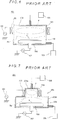
- a plasma etching apparatus 101 of the prior-art example 1 has a cylindrical chamber 102 having a plasma generating space 109 defined at the upper side and a processing space 110 defined at the lower side, a coil 103 disposed on the outside of the chamber 102 corresponding to the plasma generating space 109 in such a manner that it winds around the chamber 102, RF power supply means 104 for supplying RF power to the coil 103, etching gas supply means 105 for supplying an etching gas into the plasma generating space 109, a platen 106 which is disposed in the processing space 110 and on which a substrate is to be placed, RF power supply means 107 for supplying RF power to the platen 106, and exhaust means 108 for exhausting the gas within the chamber 102.
- an inductive electric field is generated in the plasma generating space 109 by applying RF power to the coli 103, plasma is generated from an etching gas supplied into the plasma generating space 109 due to this inductive electric field, and a substrate K on the platen 106 is etched by the generated plasma.
- a plasma etching apparatus 201 of the prior-art example 2 has a chamber 202, which is similarly formed in a cylindrical shape, comprising a small-diameter portion 202a at the upper side and a large-diameter portion 202b at the lower side.
- a coil 203 is disposed on the outside of the small-diameter portion 202a in such a manner that it winds around the small-diameter portion 202a, and the inside of the small-diameter portion 202a is defined as a plasma generating space 209.
- the inside of the large-diameter portion 202b is defined as a processing space 210, and a platen 206 on which a substrate is to be placed is disposed in the processing space 210.
- RF power supply means 204 supplies RF power to the coil 203, and on the other hand, RF power supply means 207 supplies RF power to the platen 206. Further, etching gas supply means 205 supplies an etching gas into the plasma generating space 209, and exhaust means 208 exhausts the gas within the chamber 202.
- this plasma etching apparatus 201 similarly to the plasma etching apparatus 101 of the prior-art example 1, an inductive electric field is generated in the plasma generating space 209 by applying RF power to the coil 203, plasma is generated from an etching gas supplied into the plasma generating space 209 due to this inductive electric field, and a substrate K on the platen 206 is etched by the generated plasma.
- the plasma etching apparatus 101 since the plasma generating space 109 is large, the plasma etching apparatus 101 can be structurally easily adapted to a relatively large substrate.
- the in-plane density Pm of the plasma generated in the plasma generating space 109 has a concave density distribution in which the density is high at the portion close to the coil 103 and is low at the central portion, and this density distribution acts on the substrate K as it is. Therefore, the surface of the substrate K is not etched uniformly.
- the etching rate is higher than that at the central portion thereof even if the in-plane density Pm of the plasma is uniform, and therefore the etching is apt to proceed fast. Therefore, in a case where the in-plane density Pm of the plasma has a concave density distribution as described above, the etching at the periphery portion of the substrate K proceeds faster and it is not possible to etch the entire surface of the substrate K uniformly.
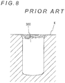
- the high plasma density at the periphery portion of the substrate K causes a problem that when a deep hole, for example, is formed in the substrate K, as shown in Fig. 8 , the periphery of the entrance of a hole 300 is etched by a high density of ions and thereby the entrance is formed into a tapered shape and the surface thereof becomes rough because of sputtering, which results in deterioration of etching shape.
- the volume of the plasma generating space 209 is small and therefore it is possible to generate high-density plasma even if the RF power applied to the coil 203 is low, and the in-plane density Pm of the plasma has a convex density distribution.
- the plasma generating space 209 is also made larger corresponding to the increase of the size of the substrate K, a problem similar to that in the case of the plasma etching apparatus 101 described above is caused.
- WO 2005/034163 A2 describes an apparatus and a method for plasma treating a substrate.
- the apparatus has a chamber and a plasma generator which forms a plasma from one or more gases flowing within the chamber so as to produce one or more species for interacting with the substrate placed within the chamber.
- a guide is provided for directing the gas flow containing the species towards the substrate. When in use, the width of the plasma is greater than that of the substrate by an amount defining an outer region of plasma.
- the guide is adapted to direct the species from at least substantially all of the outer region of the plasma towards the substrate.
- the present invention has been achieved in view of the above-described circumstances, and an object thereof is to provide a substrate processing apparatus capable of etching the entire surface of a substrate uniformly even if the substrate is large-sized and capable of preventing a deterioration of shape caused by ions.
- the present invention for solving the above-described problem, provides a plasma etching apparatus with the features of claim 1.
- this plasma etching apparatus first of all, RF power is applied to the coil by the power supply means for coil. Thereby, an inductive electric field is generated in the plasma generating space in the chamber. Under this condition, when a processing gas is supplied into the plasma generating space by the processing gas supply means, plasma is generated form the supplied processing gas due to the inductive electric field.
- the in-plane density of the plasma thus generated has a concave density distribution in which the density is high at the periphery portion which is close to the coil and the density is low at the central portion.
- the plasma having such a concave density distribution flows downward and flows through the cylindrical plasma density adjusting member having an opening at the top and an opening at the bottom, reaches a substrate placed on the platen which is positioned below the plasma density adjusting member, and etches the surface of the substrate.
- the plasma density adjusting member is formed in a funnel shape the lower end portion of which has an inner diameter smaller than the inner diameter of the upper end portion thereof and than the inner diameter of the body portion forming the plasma generating space, the in-plane density of the plasma which has an extremely concave density distribution is equalized or is adjusted to have a somewhat convex density distribution in reverse by flowing the plasma through the plasma density adjusting member, after which the plasma reaches the substrate.
- the density of the plasma generated in the plasma generating space is high at the periphery portion thereof, that is, the ion density is also high there, since the plasma density adjusting member of the present invention is made of a conductive material grounded, a high density of ions existing at the periphery portion of the plasma is neutralized by contacting with the plasma density adjusting member while the plasma passes through the plasma density adjusting member, and thereby the ion density at the periphery portion is reduced.
- an object of the present invention is to etch the entire surface of a substrate uniformly even if the substrate is large-sized, that is, to equalize the etching rate throughout the entire surface of a substrate.
- the in-plane density of the plasma has a gradual concave density distribution or a gradual convex density distribution depending on various conditions such as mask opening ratio of substrate, substrate size etc.
- a cylindrical core member at the central portion of the top plate, which core member hangs downward from the top plate to form the plasma generating space in a doughnut shape.
- the core member is made of a non-conductive material.
- the core member is made of a conductive material and is provided, ions in the plasma generated in the plasma generating space disappear, and, as a result thereof, the plasma density is reduced.
- the core member is made of a non-conductive material, it is possible to prevent the reduction of the plasma density.
- the in-plane density of plasma can be adjusted to become in a most suitable state by flowing the plasma through said plasma density adjusting member, and, as a result thereof, it is possible to etch the entire surface of a substrate uniformly.
- a plasma etching apparatus 1 of the embodiment has a chamber 2 comprising a lower body portion 3, an upper body portion 7, a bottom plate 4, an intermediate plate 5, and a top plate 8.
- the lower body portion 3, the upper body portion 7, the bottom plate 4, the intermediate plate 5 and the top plate 8 are each made of a non-conductive material (for example, ceramics), and the upper body portion 7 and the lower body portion 3 are formed in a cylindrical shape.
- the bottom plate 4 is fixed on the lower end portion of the lower body portion 3 and the intermediate plate 5 is fixed on the upper end portion of the lower body portion 3, and the lower body portion 3, the bottom plate 4 and the intermediate plate 5 form a processing space 6.
- a platen 10 is disposed on which a substrate K is to be placed and the platen 10 is lifted up and down by an appropriate lifting mechanism.
- An RF power supply unit 13 is connected to the platen 10 via a matching unit 14, and RF power is supplied to the platen 10 by the RF power supply unit 13.
- the reference numeral 11 indicates a cover covering the outer peripheral portion of the platen 10 and the reference numeral 12 indicates a support for supporting the lifting of the platen 10.
- the lower body portion 3 has an opening 3a for loading and unloading the substrate K and an exhaust port 3b for exhausting the gas within the processing space 6 formed therein.
- the opening 3a is opened and closed by a shutter mechanism 21, and the exhaust port 3b is connected to an exhaust device 22 and the gas within the processing space 6 is exhausted by the exhaust device 22.
- the upper body portion 7 is fixed on the intermediate plate 5 and the top plate 8 is fixed on the upper end portion of the upper body portion 7.
- a cup-shaped core member 15 is fixed on the central portion of the top plate 8.
- a doughnut-shaped plasma generating space 9 is formed by the upper body portion 7, the top plate 8 and the core member 15. It is noted that the inner diameter of the upper body portion 7 is larger than the outer diameter of the substrate K.
- the intermediate plate 5 has an opening 5a formed therein and a plasma density adjusting member 20 which is formed in a funnel shape having an opening at the top and an opening at the bottom is fixedly provided on the lower surface of the intermediate plate 5.
- the plasma generating space 9 and the processing space 6 communicate with each other via the opening 5a and the plasma density adjusting member 20.
- the plasma density adjusting member 20 is positioned between the plasma generating space 9 and the substrate K, and is made of a conductive material (for example, aluminum) and is appropriately grounded. Further, the inner diameter of the lower end portion of the plasma density adjusting member is smaller than the inner diameter of the upper body portion 7.
- a coil 16 is disposed on the outside of the upper body portion 7 in such a manner that it winds around the upper body portion 7, and is connected to an RF power supply unit 17 via a matching unit 18.
- the RF power supply unit 17 supplies RF power to the coil 16.
- a supply pipe 19a connecting to an etching gas supply source 19 is connected to the top plate 5, and an etching gas is supplied into the plasma generating space 9 from the etching gas supply source 19.
- a substrate K for example, a silicon substrate
- the platen 10 is lifted up to a processing position and the processing space 6 and the plasma processing space 9 are brought to a negative pressure by the exhaust device 22, and RF power is supplied to the platen 10 from the RF power supply unit 13.
- RF power is supplied to the coil 16 from the RF power supply unit 17, and thereby an inductive electric field is generated in the plasma generating space 9.
- an etching gas for example, SF 6 gas
- plasma is generated from the etching gas due to the inductive electric field.
- the plasma generating space 9 is, as described above, formed in a doughnut shape by the cylindrical core member 15, the volume thereof is small. Further, since only the region close to the coil 16 is defined as the plasma generating space 9, high-density plasma can be generated even when the power applied to the coil 16 is relatively low.
- the high-density plasma thus generated flows downward and flows through the plasma density adjusting member 20, and reaches the substrate K positioned below the plasma density adjusting member 20 and etches the surface of the substrate K. It is noted that the in-plane density of the plasma flowing downward from the plasma generating space 9 has a concave density distribution in which the density is extremely high at the periphery portion and is low at the central portion.
- the plasma density adjusting member 20 is formed in a funnel shape the lower opening of which has an inner diameter smaller than the inner diameter of the upper body portion 7, the plasma is gradually concentrated and the in-plane density thereof is gradually equalized, and thereby the in-plane density of the plasma is adjusted to have a gradual concave density distribution or to have a flat uniform density distribution or to have a gradual convex density distribution, after which the plasma reaches the substrate.
- the high-density plasma adjusted as described above acts on the surface of the substrate, and thereby the entire surface of the substrate is etched uniformly.
- a bias potential is applied to the substrate K by applying RF power to the platen 10. Therefore, ions in the plasma are irradiated toward the substrate K, and thereby so-called ion assisted etching is performed.
- the plasma density adjusting member 20 is made of a conductive material grounded, while the plasma passes through the plasma density adjusting member 20, a high density of ions existing at the periphery portion of the plasma is neutralized by contacting with the plasma density adjusting member 20, and thereby disappears. Therefore, the problem that deterioration of etching shape is resulted from a high density of ions acting on the substrate is solved.
- Fig. 2 shows the result of the formation of a deep hole in the substrate K using the plasma etching apparatus 1 of the embodiment.
- the entrance of a hole 30 is not formed into a tapered shape and further the surface thereof is not rough.
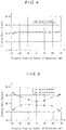
- Fig. 4 shows the result of the etching of a SiO 2 film on a silicon substrate of 6 inches, wherein the plasma etching apparatus 1 of the embodiment as shown in Fig. 1 was used, SF 6 gas was used as etching gas, the flow rate of the SF 6 gas supplied into the plasma generating space 9 was 500 ml/min, the RF power applied to the coil 16 was 2000 W, the RF power applied to the platen 10 was 70 W, and the dimensions of the plasma density adjusting member 20 as shown in Fig. 3 , that is, the lower-end inner diameter D 1 , upper-end inner diameter D 2 and length L thereof were 172 mm, 270 mm and 106 mm, respectively.
- the entire surface of the substrate K could be etched with an extremely high etching-rate uniformity of 15.5 nm/min ⁇ 3.1 %.
- Fig. 5 shows the result of the etching when the D 1 and the length L of the plasma density adjusting member 20 were set to 165 mm and 86 mm, respectively and the result of the etching when the D 1 and the length L of the plasma density adjusting member 20 were set to 242 mm and 86 mm, respectively.
- the etching rate throughout the entire surface of the substrate K was 17.8 nm/min ⁇ 10.1 % when the D 1 was 165 mm, and the etching rate throughout the entire surface of the substrate K was 23.9 nm/min ⁇ 11.1 % when the D 1 was 242 mm.
- adjusting the dimensions of the plasma density adjusting member 20 appropriately enables the entire surface of the substrate K to be processed uniformly. Further, as seen from Fig. 4 , setting the dimensions of the plasma density adjusting member 20 to the optimum conditions enables the entire surface of the substrate K to be etched with an extremely high uniformity.
- the core member 15 is preferably made of a non-conductive material.
- the core member 15 is made of a conductive material and is provided, ions in the plasma generated in the plasma generating space 9 disappear, and, as a result thereof, the density of the plasma is reduced.
- the core member 15 is made of a non-conductive material, it is possible to prevent the reduction of the density of the plasma.
- the plasma etching apparatus of the present invention can be suitably used as a plasma etching apparatus capable of etching the entire surface of a substrate with an extremely high uniformity.
Landscapes
- Physics & Mathematics (AREA)
- Engineering & Computer Science (AREA)
- Plasma & Fusion (AREA)
- Chemical & Material Sciences (AREA)
- Analytical Chemistry (AREA)
- Plasma Technology (AREA)
- Drying Of Semiconductors (AREA)
- Paper (AREA)
Applications Claiming Priority (2)
| Application Number | Priority Date | Filing Date | Title |
|---|---|---|---|
| JP2009084137A JP4977730B2 (ja) | 2009-03-31 | 2009-03-31 | プラズマエッチング装置 |
| PCT/JP2009/070643 WO2010113358A1 (ja) | 2009-03-31 | 2009-12-10 | プラズマエッチング装置 |
Publications (3)
| Publication Number | Publication Date |
|---|---|
| EP2416351A1 EP2416351A1 (en) | 2012-02-08 |
| EP2416351A4 EP2416351A4 (en) | 2015-08-12 |
| EP2416351B1 true EP2416351B1 (en) | 2019-08-07 |
Family
ID=42827680
Family Applications (1)
| Application Number | Title | Priority Date | Filing Date |
|---|---|---|---|
| EP09842709.9A Active EP2416351B1 (en) | 2009-03-31 | 2009-12-10 | Plasma etching apparatus |
Country Status (7)
| Country | Link |
|---|---|
| US (1) | US20120006490A1 (enExample) |
| EP (1) | EP2416351B1 (enExample) |
| JP (1) | JP4977730B2 (enExample) |
| KR (1) | KR20120009419A (enExample) |
| CN (1) | CN102301457B (enExample) |
| TW (1) | TWI476829B (enExample) |
| WO (1) | WO2010113358A1 (enExample) |
Families Citing this family (9)
| Publication number | Priority date | Publication date | Assignee | Title |
|---|---|---|---|---|
| WO2013028313A1 (en) * | 2011-08-19 | 2013-02-28 | Mattson Technology, Inc. | High efficiency plasma source |
| JP5821039B2 (ja) * | 2011-11-07 | 2015-11-24 | パナソニックIpマネジメント株式会社 | プラズマ処理装置 |
| JP5485327B2 (ja) * | 2012-04-16 | 2014-05-07 | Sppテクノロジーズ株式会社 | プラズマ密度調整部材 |
| CN104871297B (zh) * | 2012-09-27 | 2017-07-18 | Spp科技股份有限公司 | 等离子蚀刻装置 |
| GB201318249D0 (en) * | 2013-10-15 | 2013-11-27 | Spts Technologies Ltd | Plasma etching apparatus |
| DE102014216195A1 (de) * | 2014-08-14 | 2016-02-18 | Robert Bosch Gmbh | Vorrichtung zum anisotropen Ätzen eines Substrats und Verfahren zum Betreiben einer Vorrichtung zum anisotropen Ätzen eines Substrats |
| JP6444794B2 (ja) * | 2015-03-30 | 2018-12-26 | Sppテクノロジーズ株式会社 | 半導体素子の製造方法及びその製造に用いられるプラズマエッチング装置 |
| US11201036B2 (en) | 2017-06-09 | 2021-12-14 | Beijing E-Town Semiconductor Technology Co., Ltd | Plasma strip tool with uniformity control |
| KR20260040116A (ko) | 2020-08-28 | 2026-03-23 | 매슨 테크놀로지 인크 | 이동가능한 인서트를 갖는 플라즈마 스트립 툴 |
Citations (1)
| Publication number | Priority date | Publication date | Assignee | Title |
|---|---|---|---|---|
| US20030092278A1 (en) * | 2001-11-13 | 2003-05-15 | Fink Steven T. | Plasma baffle assembly |
Family Cites Families (9)
| Publication number | Priority date | Publication date | Assignee | Title |
|---|---|---|---|---|
| JP2001007083A (ja) * | 1999-06-18 | 2001-01-12 | Sony Corp | プラズマ処理装置及び方法 |
| EP1162646A3 (en) * | 2000-06-06 | 2004-10-13 | Matsushita Electric Works, Ltd. | Plasma treatment apparatus and method |
| EP1444726A4 (en) * | 2001-10-22 | 2008-08-13 | Unaxis Usa Inc | METHOD AND DEVICE FOR Etching PHOTOMASCIC SUBSTRATES USING PULSED PLASMA |
| JP2004079465A (ja) * | 2002-08-22 | 2004-03-11 | Shimadzu Corp | プラズマ生成装置およびプラズマ処理装置 |
| JP3712125B2 (ja) * | 2003-02-03 | 2005-11-02 | 東京応化工業株式会社 | プラズマ処理装置 |
| GB0323001D0 (en) * | 2003-10-01 | 2003-11-05 | Oxford Instr Plasma Technology | Apparatus and method for plasma treating a substrate |
| JP4459877B2 (ja) | 2004-08-12 | 2010-04-28 | 住友精密工業株式会社 | エッチング方法及びエッチング装置 |
| JP4578893B2 (ja) | 2004-08-20 | 2010-11-10 | 住友精密工業株式会社 | シリコン材のプラズマエッチング方法及びプラズマエッチング装置 |
| KR100683174B1 (ko) * | 2005-06-17 | 2007-02-15 | 삼성전자주식회사 | 플라즈마 가속장치 및 그것을 구비하는 플라즈마 처리시스템 |
-
2009
- 2009-03-31 JP JP2009084137A patent/JP4977730B2/ja active Active
- 2009-12-10 US US13/145,228 patent/US20120006490A1/en not_active Abandoned
- 2009-12-10 WO PCT/JP2009/070643 patent/WO2010113358A1/ja not_active Ceased
- 2009-12-10 EP EP09842709.9A patent/EP2416351B1/en active Active
- 2009-12-10 KR KR1020117015433A patent/KR20120009419A/ko not_active Ceased
- 2009-12-10 CN CN2009801552603A patent/CN102301457B/zh active Active
- 2009-12-16 TW TW098143187A patent/TWI476829B/zh active
Patent Citations (1)
| Publication number | Priority date | Publication date | Assignee | Title |
|---|---|---|---|---|
| US20030092278A1 (en) * | 2001-11-13 | 2003-05-15 | Fink Steven T. | Plasma baffle assembly |
Also Published As
| Publication number | Publication date |
|---|---|
| US20120006490A1 (en) | 2012-01-12 |
| EP2416351A1 (en) | 2012-02-08 |
| CN102301457B (zh) | 2013-09-25 |
| JP4977730B2 (ja) | 2012-07-18 |
| WO2010113358A1 (ja) | 2010-10-07 |
| TW201036061A (en) | 2010-10-01 |
| CN102301457A (zh) | 2011-12-28 |
| KR20120009419A (ko) | 2012-01-31 |
| EP2416351A4 (en) | 2015-08-12 |
| JP2010238847A (ja) | 2010-10-21 |
| TWI476829B (zh) | 2015-03-11 |
Similar Documents
| Publication | Publication Date | Title |
|---|---|---|
| EP2416351B1 (en) | Plasma etching apparatus | |
| EP2479781B1 (en) | Plasma etching method | |
| KR101331420B1 (ko) | 기판 처리 장치 및 반도체 장치의 제조 방법 | |
| US10504697B2 (en) | Particle generation suppresor by DC bias modulation | |
| KR102188404B1 (ko) | 정전 척의 개질 방법 및 플라즈마 처리 장치 | |
| KR101495288B1 (ko) | 기판 처리 장치 및 방법 | |
| US8864936B2 (en) | Apparatus and method for processing substrate | |
| KR102116474B1 (ko) | 기판 처리 장치 및 기판 처리 방법 | |
| US6306247B1 (en) | Apparatus and method for preventing etch chamber contamination | |
| JP2015050362A (ja) | プラズマ処理装置 | |
| TWI828704B (zh) | 電漿處理方法與用於電漿處理腔室的腔室部件及其製造方法 | |
| JP2008235611A (ja) | プラズマ処理装置及びプラズマ処理方法 | |
| JP5232512B2 (ja) | プラズマ処理装置及びプラズマ処理方法 | |
| JP5893260B2 (ja) | プラズマ処理装置および処理方法 | |
| KR101559874B1 (ko) | 기판 처리 장치 및 챔버 제조 방법 | |
| JP2021077837A (ja) | 基板処理装置 | |
| JP4865352B2 (ja) | プラズマ処理装置及びプラズマ処理方法 | |
| JP5485327B2 (ja) | プラズマ密度調整部材 | |
| JP2012169652A (ja) | プラズマエッチング方法 | |
| KR102275509B1 (ko) | 지지 유닛 및 기판 처리 장치 | |
| CN104347337A (zh) | 刻蚀机和利用刻蚀机刻蚀晶片的方法 | |
| JP2007103697A (ja) | 基板処理装置 | |
| KR20260011891A (ko) | 기판 처리 방법 및 기판 처리 장치 | |
| JP2005093886A (ja) | 半導体製造装置 | |
| JP2009059845A (ja) | 基板処理装置 |
Legal Events
| Date | Code | Title | Description |
|---|---|---|---|
| PUAI | Public reference made under article 153(3) epc to a published international application that has entered the european phase |
Free format text: ORIGINAL CODE: 0009012 |
|
| 17P | Request for examination filed |
Effective date: 20110830 |
|
| AK | Designated contracting states |
Kind code of ref document: A1 Designated state(s): AT BE BG CH CY CZ DE DK EE ES FI FR GB GR HR HU IE IS IT LI LT LU LV MC MK MT NL NO PL PT RO SE SI SK SM TR |
|
| RAP1 | Party data changed (applicant data changed or rights of an application transferred) |
Owner name: SPP TECHNOLOGIES CO., LTD. |
|
| DAX | Request for extension of the european patent (deleted) | ||
| RAP1 | Party data changed (applicant data changed or rights of an application transferred) |
Owner name: SPP TECHNOLOGIES CO., LTD. |
|
| RA4 | Supplementary search report drawn up and despatched (corrected) |
Effective date: 20150715 |
|
| RIC1 | Information provided on ipc code assigned before grant |
Ipc: H05H 1/46 20060101ALI20150709BHEP Ipc: H01J 37/32 20060101ALI20150709BHEP Ipc: H01L 21/3065 20060101AFI20150709BHEP |
|
| STAA | Information on the status of an ep patent application or granted ep patent |
Free format text: STATUS: EXAMINATION IS IN PROGRESS |
|
| 17Q | First examination report despatched |
Effective date: 20181008 |
|
| GRAP | Despatch of communication of intention to grant a patent |
Free format text: ORIGINAL CODE: EPIDOSNIGR1 |
|
| STAA | Information on the status of an ep patent application or granted ep patent |
Free format text: STATUS: GRANT OF PATENT IS INTENDED |
|
| INTG | Intention to grant announced |
Effective date: 20190327 |
|
| GRAS | Grant fee paid |
Free format text: ORIGINAL CODE: EPIDOSNIGR3 |
|
| GRAA | (expected) grant |
Free format text: ORIGINAL CODE: 0009210 |
|
| STAA | Information on the status of an ep patent application or granted ep patent |
Free format text: STATUS: THE PATENT HAS BEEN GRANTED |
|
| AK | Designated contracting states |
Kind code of ref document: B1 Designated state(s): AT BE BG CH CY CZ DE DK EE ES FI FR GB GR HR HU IE IS IT LI LT LU LV MC MK MT NL NO PL PT RO SE SI SK SM TR |
|
| REG | Reference to a national code |
Ref country code: GB Ref legal event code: FG4D |
|
| REG | Reference to a national code |
Ref country code: CH Ref legal event code: EP Ref country code: AT Ref legal event code: REF Ref document number: 1165134 Country of ref document: AT Kind code of ref document: T Effective date: 20190815 |
|
| REG | Reference to a national code |
Ref country code: DE Ref legal event code: R096 Ref document number: 602009059410 Country of ref document: DE |
|
| REG | Reference to a national code |
Ref country code: IE Ref legal event code: FG4D |
|
| REG | Reference to a national code |
Ref country code: NL Ref legal event code: MP Effective date: 20190807 |
|
| REG | Reference to a national code |
Ref country code: LT Ref legal event code: MG4D |
|
| PG25 | Lapsed in a contracting state [announced via postgrant information from national office to epo] |
Ref country code: LT Free format text: LAPSE BECAUSE OF FAILURE TO SUBMIT A TRANSLATION OF THE DESCRIPTION OR TO PAY THE FEE WITHIN THE PRESCRIBED TIME-LIMIT Effective date: 20190807 Ref country code: FI Free format text: LAPSE BECAUSE OF FAILURE TO SUBMIT A TRANSLATION OF THE DESCRIPTION OR TO PAY THE FEE WITHIN THE PRESCRIBED TIME-LIMIT Effective date: 20190807 Ref country code: NL Free format text: LAPSE BECAUSE OF FAILURE TO SUBMIT A TRANSLATION OF THE DESCRIPTION OR TO PAY THE FEE WITHIN THE PRESCRIBED TIME-LIMIT Effective date: 20190807 Ref country code: SE Free format text: LAPSE BECAUSE OF FAILURE TO SUBMIT A TRANSLATION OF THE DESCRIPTION OR TO PAY THE FEE WITHIN THE PRESCRIBED TIME-LIMIT Effective date: 20190807 Ref country code: PT Free format text: LAPSE BECAUSE OF FAILURE TO SUBMIT A TRANSLATION OF THE DESCRIPTION OR TO PAY THE FEE WITHIN THE PRESCRIBED TIME-LIMIT Effective date: 20191209 Ref country code: HR Free format text: LAPSE BECAUSE OF FAILURE TO SUBMIT A TRANSLATION OF THE DESCRIPTION OR TO PAY THE FEE WITHIN THE PRESCRIBED TIME-LIMIT Effective date: 20190807 Ref country code: BG Free format text: LAPSE BECAUSE OF FAILURE TO SUBMIT A TRANSLATION OF THE DESCRIPTION OR TO PAY THE FEE WITHIN THE PRESCRIBED TIME-LIMIT Effective date: 20191107 Ref country code: NO Free format text: LAPSE BECAUSE OF FAILURE TO SUBMIT A TRANSLATION OF THE DESCRIPTION OR TO PAY THE FEE WITHIN THE PRESCRIBED TIME-LIMIT Effective date: 20191107 |
|
| REG | Reference to a national code |
Ref country code: AT Ref legal event code: MK05 Ref document number: 1165134 Country of ref document: AT Kind code of ref document: T Effective date: 20190807 |
|
| PG25 | Lapsed in a contracting state [announced via postgrant information from national office to epo] |
Ref country code: IS Free format text: LAPSE BECAUSE OF FAILURE TO SUBMIT A TRANSLATION OF THE DESCRIPTION OR TO PAY THE FEE WITHIN THE PRESCRIBED TIME-LIMIT Effective date: 20191207 Ref country code: ES Free format text: LAPSE BECAUSE OF FAILURE TO SUBMIT A TRANSLATION OF THE DESCRIPTION OR TO PAY THE FEE WITHIN THE PRESCRIBED TIME-LIMIT Effective date: 20190807 Ref country code: LV Free format text: LAPSE BECAUSE OF FAILURE TO SUBMIT A TRANSLATION OF THE DESCRIPTION OR TO PAY THE FEE WITHIN THE PRESCRIBED TIME-LIMIT Effective date: 20190807 Ref country code: GR Free format text: LAPSE BECAUSE OF FAILURE TO SUBMIT A TRANSLATION OF THE DESCRIPTION OR TO PAY THE FEE WITHIN THE PRESCRIBED TIME-LIMIT Effective date: 20191108 |
|
| PG25 | Lapsed in a contracting state [announced via postgrant information from national office to epo] |
Ref country code: TR Free format text: LAPSE BECAUSE OF FAILURE TO SUBMIT A TRANSLATION OF THE DESCRIPTION OR TO PAY THE FEE WITHIN THE PRESCRIBED TIME-LIMIT Effective date: 20190807 |
|
| PG25 | Lapsed in a contracting state [announced via postgrant information from national office to epo] |
Ref country code: DK Free format text: LAPSE BECAUSE OF FAILURE TO SUBMIT A TRANSLATION OF THE DESCRIPTION OR TO PAY THE FEE WITHIN THE PRESCRIBED TIME-LIMIT Effective date: 20190807 Ref country code: AT Free format text: LAPSE BECAUSE OF FAILURE TO SUBMIT A TRANSLATION OF THE DESCRIPTION OR TO PAY THE FEE WITHIN THE PRESCRIBED TIME-LIMIT Effective date: 20190807 Ref country code: EE Free format text: LAPSE BECAUSE OF FAILURE TO SUBMIT A TRANSLATION OF THE DESCRIPTION OR TO PAY THE FEE WITHIN THE PRESCRIBED TIME-LIMIT Effective date: 20190807 Ref country code: PL Free format text: LAPSE BECAUSE OF FAILURE TO SUBMIT A TRANSLATION OF THE DESCRIPTION OR TO PAY THE FEE WITHIN THE PRESCRIBED TIME-LIMIT Effective date: 20190807 Ref country code: RO Free format text: LAPSE BECAUSE OF FAILURE TO SUBMIT A TRANSLATION OF THE DESCRIPTION OR TO PAY THE FEE WITHIN THE PRESCRIBED TIME-LIMIT Effective date: 20190807 Ref country code: IT Free format text: LAPSE BECAUSE OF FAILURE TO SUBMIT A TRANSLATION OF THE DESCRIPTION OR TO PAY THE FEE WITHIN THE PRESCRIBED TIME-LIMIT Effective date: 20190807 |
|
| PG25 | Lapsed in a contracting state [announced via postgrant information from national office to epo] |
Ref country code: SM Free format text: LAPSE BECAUSE OF FAILURE TO SUBMIT A TRANSLATION OF THE DESCRIPTION OR TO PAY THE FEE WITHIN THE PRESCRIBED TIME-LIMIT Effective date: 20190807 Ref country code: IS Free format text: LAPSE BECAUSE OF FAILURE TO SUBMIT A TRANSLATION OF THE DESCRIPTION OR TO PAY THE FEE WITHIN THE PRESCRIBED TIME-LIMIT Effective date: 20200224 Ref country code: SK Free format text: LAPSE BECAUSE OF FAILURE TO SUBMIT A TRANSLATION OF THE DESCRIPTION OR TO PAY THE FEE WITHIN THE PRESCRIBED TIME-LIMIT Effective date: 20190807 Ref country code: CZ Free format text: LAPSE BECAUSE OF FAILURE TO SUBMIT A TRANSLATION OF THE DESCRIPTION OR TO PAY THE FEE WITHIN THE PRESCRIBED TIME-LIMIT Effective date: 20190807 |
|
| REG | Reference to a national code |
Ref country code: DE Ref legal event code: R097 Ref document number: 602009059410 Country of ref document: DE |
|
| PLBE | No opposition filed within time limit |
Free format text: ORIGINAL CODE: 0009261 |
|
| STAA | Information on the status of an ep patent application or granted ep patent |
Free format text: STATUS: NO OPPOSITION FILED WITHIN TIME LIMIT |
|
| PG2D | Information on lapse in contracting state deleted |
Ref country code: IS |
|
| REG | Reference to a national code |
Ref country code: CH Ref legal event code: PL |
|
| 26N | No opposition filed |
Effective date: 20200603 |
|
| REG | Reference to a national code |
Ref country code: BE Ref legal event code: MM Effective date: 20191231 |
|
| PG25 | Lapsed in a contracting state [announced via postgrant information from national office to epo] |
Ref country code: SI Free format text: LAPSE BECAUSE OF FAILURE TO SUBMIT A TRANSLATION OF THE DESCRIPTION OR TO PAY THE FEE WITHIN THE PRESCRIBED TIME-LIMIT Effective date: 20190807 Ref country code: MC Free format text: LAPSE BECAUSE OF FAILURE TO SUBMIT A TRANSLATION OF THE DESCRIPTION OR TO PAY THE FEE WITHIN THE PRESCRIBED TIME-LIMIT Effective date: 20190807 |
|
| PG25 | Lapsed in a contracting state [announced via postgrant information from national office to epo] |
Ref country code: IE Free format text: LAPSE BECAUSE OF NON-PAYMENT OF DUE FEES Effective date: 20191210 Ref country code: LU Free format text: LAPSE BECAUSE OF NON-PAYMENT OF DUE FEES Effective date: 20191210 |
|
| PG25 | Lapsed in a contracting state [announced via postgrant information from national office to epo] |
Ref country code: LI Free format text: LAPSE BECAUSE OF NON-PAYMENT OF DUE FEES Effective date: 20191231 Ref country code: BE Free format text: LAPSE BECAUSE OF NON-PAYMENT OF DUE FEES Effective date: 20191231 Ref country code: CH Free format text: LAPSE BECAUSE OF NON-PAYMENT OF DUE FEES Effective date: 20191231 |
|
| PG25 | Lapsed in a contracting state [announced via postgrant information from national office to epo] |
Ref country code: CY Free format text: LAPSE BECAUSE OF FAILURE TO SUBMIT A TRANSLATION OF THE DESCRIPTION OR TO PAY THE FEE WITHIN THE PRESCRIBED TIME-LIMIT Effective date: 20190807 |
|
| PG25 | Lapsed in a contracting state [announced via postgrant information from national office to epo] |
Ref country code: MT Free format text: LAPSE BECAUSE OF FAILURE TO SUBMIT A TRANSLATION OF THE DESCRIPTION OR TO PAY THE FEE WITHIN THE PRESCRIBED TIME-LIMIT Effective date: 20190807 Ref country code: HU Free format text: LAPSE BECAUSE OF FAILURE TO SUBMIT A TRANSLATION OF THE DESCRIPTION OR TO PAY THE FEE WITHIN THE PRESCRIBED TIME-LIMIT; INVALID AB INITIO Effective date: 20091210 |
|
| PG25 | Lapsed in a contracting state [announced via postgrant information from national office to epo] |
Ref country code: MK Free format text: LAPSE BECAUSE OF FAILURE TO SUBMIT A TRANSLATION OF THE DESCRIPTION OR TO PAY THE FEE WITHIN THE PRESCRIBED TIME-LIMIT Effective date: 20190807 |
|
| REG | Reference to a national code |
Ref country code: DE Ref legal event code: R079 Ref document number: 602009059410 Country of ref document: DE Free format text: PREVIOUS MAIN CLASS: H01L0021306500 Ipc: H10P0050240000 |
|
| PGFP | Annual fee paid to national office [announced via postgrant information from national office to epo] |
Ref country code: DE Payment date: 20251028 Year of fee payment: 17 |
|
| PGFP | Annual fee paid to national office [announced via postgrant information from national office to epo] |
Ref country code: GB Payment date: 20251030 Year of fee payment: 17 |
|
| PGFP | Annual fee paid to national office [announced via postgrant information from national office to epo] |
Ref country code: FR Payment date: 20251110 Year of fee payment: 17 |