EP2413488A1 - Procédé de commande d'un appareil de conversion de puissance - Google Patents
Procédé de commande d'un appareil de conversion de puissance Download PDFInfo
- Publication number
- EP2413488A1 EP2413488A1 EP10764511A EP10764511A EP2413488A1 EP 2413488 A1 EP2413488 A1 EP 2413488A1 EP 10764511 A EP10764511 A EP 10764511A EP 10764511 A EP10764511 A EP 10764511A EP 2413488 A1 EP2413488 A1 EP 2413488A1
- Authority
- EP
- European Patent Office
- Prior art keywords
- voltage command
- signal
- correction amount
- command values
- value
- Prior art date
- Legal status (The legal status is an assumption and is not a legal conclusion. Google has not performed a legal analysis and makes no representation as to the accuracy of the status listed.)
- Withdrawn
Links
Images


Classifications
-
- H—ELECTRICITY
- H02—GENERATION; CONVERSION OR DISTRIBUTION OF ELECTRIC POWER
- H02M—APPARATUS FOR CONVERSION BETWEEN AC AND AC, BETWEEN AC AND DC, OR BETWEEN DC AND DC, AND FOR USE WITH MAINS OR SIMILAR POWER SUPPLY SYSTEMS; CONVERSION OF DC OR AC INPUT POWER INTO SURGE OUTPUT POWER; CONTROL OR REGULATION THEREOF
- H02M7/00—Conversion of ac power input into dc power output; Conversion of dc power input into ac power output
- H02M7/42—Conversion of dc power input into ac power output without possibility of reversal
- H02M7/44—Conversion of dc power input into ac power output without possibility of reversal by static converters
- H02M7/48—Conversion of dc power input into ac power output without possibility of reversal by static converters using discharge tubes with control electrode or semiconductor devices with control electrode
- H02M7/53—Conversion of dc power input into ac power output without possibility of reversal by static converters using discharge tubes with control electrode or semiconductor devices with control electrode using devices of a triode or transistor type requiring continuous application of a control signal
- H02M7/537—Conversion of dc power input into ac power output without possibility of reversal by static converters using discharge tubes with control electrode or semiconductor devices with control electrode using devices of a triode or transistor type requiring continuous application of a control signal using semiconductor devices only, e.g. single switched pulse inverters
- H02M7/5387—Conversion of dc power input into ac power output without possibility of reversal by static converters using discharge tubes with control electrode or semiconductor devices with control electrode using devices of a triode or transistor type requiring continuous application of a control signal using semiconductor devices only, e.g. single switched pulse inverters in a bridge configuration
- H02M7/53871—Conversion of dc power input into ac power output without possibility of reversal by static converters using discharge tubes with control electrode or semiconductor devices with control electrode using devices of a triode or transistor type requiring continuous application of a control signal using semiconductor devices only, e.g. single switched pulse inverters in a bridge configuration with automatic control of output voltage or current
- H02M7/53875—Conversion of dc power input into ac power output without possibility of reversal by static converters using discharge tubes with control electrode or semiconductor devices with control electrode using devices of a triode or transistor type requiring continuous application of a control signal using semiconductor devices only, e.g. single switched pulse inverters in a bridge configuration with automatic control of output voltage or current with analogue control of three-phase output
-
- H—ELECTRICITY
- H02—GENERATION; CONVERSION OR DISTRIBUTION OF ELECTRIC POWER
- H02M—APPARATUS FOR CONVERSION BETWEEN AC AND AC, BETWEEN AC AND DC, OR BETWEEN DC AND DC, AND FOR USE WITH MAINS OR SIMILAR POWER SUPPLY SYSTEMS; CONVERSION OF DC OR AC INPUT POWER INTO SURGE OUTPUT POWER; CONTROL OR REGULATION THEREOF
- H02M7/00—Conversion of ac power input into dc power output; Conversion of dc power input into ac power output
- H02M7/02—Conversion of ac power input into dc power output without possibility of reversal
- H02M7/04—Conversion of ac power input into dc power output without possibility of reversal by static converters
- H02M7/12—Conversion of ac power input into dc power output without possibility of reversal by static converters using discharge tubes with control electrode or semiconductor devices with control electrode
- H02M7/21—Conversion of ac power input into dc power output without possibility of reversal by static converters using discharge tubes with control electrode or semiconductor devices with control electrode using devices of a triode or transistor type requiring continuous application of a control signal
- H02M7/217—Conversion of ac power input into dc power output without possibility of reversal by static converters using discharge tubes with control electrode or semiconductor devices with control electrode using devices of a triode or transistor type requiring continuous application of a control signal using semiconductor devices only
- H02M7/219—Conversion of ac power input into dc power output without possibility of reversal by static converters using discharge tubes with control electrode or semiconductor devices with control electrode using devices of a triode or transistor type requiring continuous application of a control signal using semiconductor devices only in a bridge configuration
-
- H—ELECTRICITY
- H02—GENERATION; CONVERSION OR DISTRIBUTION OF ELECTRIC POWER
- H02M—APPARATUS FOR CONVERSION BETWEEN AC AND AC, BETWEEN AC AND DC, OR BETWEEN DC AND DC, AND FOR USE WITH MAINS OR SIMILAR POWER SUPPLY SYSTEMS; CONVERSION OF DC OR AC INPUT POWER INTO SURGE OUTPUT POWER; CONTROL OR REGULATION THEREOF
- H02M1/00—Details of apparatus for conversion
- H02M1/0003—Details of control, feedback or regulation circuits
- H02M1/0025—Arrangements for modifying reference values, feedback values or error values in the control loop of a converter
Definitions
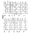
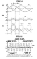
- the voltage command value V* U takes a maximum level in an interval (zone) "A”
- the voltage command value V* W takes a minimum level in an interval "B”.
- the correction amount ⁇ (waveform of FIG. 14 (b) ) is added to each of the voltage command values V* U , V* V and V* W of three phases.
- the two-arm modulation method When the three-arm modulation method is compared with the two-arm modulation method in a case that each phase is modulated by a triangular-wave carrier having an identical frequency, the two-arm modulation method generates a lower level of switching loss than the three-arm modulation method. Hence, it is more efficient to employ the two-arm modulation method.
- one aspect of the above method of controlling a power conversion device according to the present invention is characterized in that the triangular-wave-shaped signal synchronized with the first correction amount is produced by multiplying a load factor by the multiplication of the gain and the addition signal of the maximum value among the voltage command values and the minimum value.
- one aspect of the above method of controlling a power conversion device according to the present invention is characterized in that an attenuation of harmonic components and a suppression of time rate of change have been applied to the load factor by a low-pass filter and a soft-start circuit.
- the signal s1 which is outputted from the comparator 5 is equal to 1 when the maximum value max(V * ) is larger than the absolute value
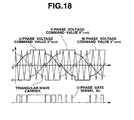
- the correction amount ⁇ that is used for the modulation method of the first embodiment is added to each of the voltage command values V* U , V* V and V* W .
- the corrected voltage command values V* U + ⁇ , V* V + ⁇ and V* W + ⁇ are obtained as shown in FIG. 3 (I) .
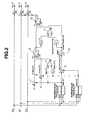
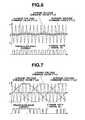
- the correction-term adder 1 of FIG. 1 is configured as shown in FIG. 2 , and the gate signal is produced by the comparison with triangular wave. By this gate signal, the ON/OFF operation of each switching element is conducted.
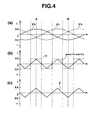
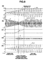
- FIG. 5(a) is a time chart of the U-phase voltage command value V* U when the modulation factor m is increased from 0 to 1.15 with the constant gradient.
- FIG. 5 (b) is a time chart of the correction amount ⁇ and the signal k(max(V * ) + min(V * )).
- FIG. 5 (c) is a time chart of the correction amount ⁇ .
- FIG. 5 (d) is a time chart of the corrected voltage command value V* U + ⁇ of U-phase in the first embodiment.
- the amplitude of the correction amount ⁇ of the two-arm modulation method becomes smaller as the modulation factor m of the voltage command value V* U becomes larger.
- the amplitude of the signal k(max(V * ) + min(V * )) becomes larger as the modulation factor m of the voltage command value V* U becomes larger.
- the modulation factor m As the modulation factor m becomes further larger, a rate of selecting of the correction amount ⁇ (which is used for the two-arm modulation method) as the correction amount ⁇ is more increased.
- the modulation factor m is equal to 1.15; whole of the correction amount ⁇ is selected as the correction amount ⁇ , i.e., the correction amount ⁇ is constituted only by the signal of correction amount ⁇ . At this time, the two-arm modulation method is completely performed.
- the modulation method can be varied continuously (not rapidly) from the three-arm modulation method to the two-arm modulation method as the modulation factor m of the voltage command value becomes large. That is, the three-arm modulation method is employed when the modulation factor m is small, and the two-arm modulation method is gradually employed as the modulation factor m becomes larger.
- the mixture ratio between the three-arm modulation method and the two-arm modulation method is varied in accordance with a magnitude of the modulation factor m.
- the mixture ratio between the three-arm modulation method and the two-arm modulation method is varied in accordance with not only the modulation factor m but also a load factor I of the power conversion device.
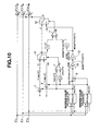
- the correction amount ⁇ is produced from the correction amount ⁇ and the signal kl(max(V * ) + min(V * )) in the switch 12 by selecting smaller one of absolute values of the correction amount ⁇ and the signal kl(max(V * ) + min(V * )).
- This switch 12 sets the signal s2 at 1 at the time of satisfaction of
- the produced correction amount ⁇ is added to the voltage command value V* so that the corrected voltage command value V* + ⁇ is produced.
- the other configurations are similar as the first embodiment.
- an amplitude of the signal kl(max(V * ) + min(V * )) becomes larger as the load factor I becomes higher.
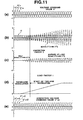
- the correction amount ⁇ shown in FIG. 11 (c) is produced by selecting from the correction amount ⁇ and the signal kl(max(V * ) + min(V * )) by means of smaller-one selection in absolute value.
- smaller one in absolute value is selected from the correction amount ⁇ and the signal kl(max(V * ) + min(V * )
- only the signal kl(max(V * ) + min(V * )) is selected as the correction amount ⁇ in a region (interval) where the load factor I is small.
- the three-arm modulation method is realized when the load factor I is small, on the other hand, the two-arm modulation method is realized when the load factor I is large. That is, a changeover between the three-arm modulation method and the two-arm modulation method can be attained according to the load factor I.
- the three-arm modulation is employed because the switching loss Wsw is small. At this time, the noise and the harmonic components can be reduced.
- the load factor I is high, the two-arm modulation is employed. At this time, the switching loss Wsw can be reduced.
- the third embodiment is applied to, for example, a power conversion device such as a solar power conditioner system (PCS) in which a variation of the load factor I is gentle.
- PCS solar power conditioner system
- the load factor I is simply multiplied by the signal k(max(V * ) + min(V * )).
- the load factor I of an uninterruptible power supply system, an instantaneous-voltage-drop compensating device or the like rapidly rises when a power failure (power outage) or the like occurs.
- the control method of the third embodiment is applied to a power conversion device causing such a rapid change of the load factor I, the three-arm modulation method is rapidly changed into the two-arm modulation method at the time of rapid change of the load factor I. As a result, a high stress is given to the device.
Landscapes
- Engineering & Computer Science (AREA)
- Power Engineering (AREA)
- Inverter Devices (AREA)
- Rectifiers (AREA)
- Ac-Ac Conversion (AREA)
Applications Claiming Priority (2)
| Application Number | Priority Date | Filing Date | Title |
|---|---|---|---|
| JP2009099491 | 2009-04-16 | ||
| PCT/JP2010/056786 WO2010119929A1 (fr) | 2009-04-16 | 2010-04-15 | Procédé de commande d'un appareil de conversion de puissance |
Publications (2)
| Publication Number | Publication Date |
|---|---|
| EP2413488A1 true EP2413488A1 (fr) | 2012-02-01 |
| EP2413488A4 EP2413488A4 (fr) | 2017-08-16 |
Family
ID=42982586
Family Applications (1)
| Application Number | Title | Priority Date | Filing Date |
|---|---|---|---|
| EP10764511.1A Withdrawn EP2413488A4 (fr) | 2009-04-16 | 2010-04-15 | Procédé de commande d'un appareil de conversion de puissance |
Country Status (7)
| Country | Link |
|---|---|
| US (1) | US8659918B2 (fr) |
| EP (1) | EP2413488A4 (fr) |
| JP (1) | JP5304891B2 (fr) |
| KR (1) | KR101266278B1 (fr) |
| CN (1) | CN102396142B (fr) |
| SG (1) | SG175197A1 (fr) |
| WO (1) | WO2010119929A1 (fr) |
Cited By (2)
| Publication number | Priority date | Publication date | Assignee | Title |
|---|---|---|---|---|
| CN107112936A (zh) * | 2014-12-08 | 2017-08-29 | 株式会社日立产机系统 | 电力转换装置和电力转换装置的控制方法 |
| EP3439163A4 (fr) * | 2016-03-28 | 2019-06-19 | Mitsubishi Electric Corporation | Convertisseur de puissance |
Families Citing this family (8)
| Publication number | Priority date | Publication date | Assignee | Title |
|---|---|---|---|---|
| JP5161985B2 (ja) | 2011-02-16 | 2013-03-13 | 三菱電機株式会社 | 電力変換装置および電動パワーステアリングの制御装置 |
| WO2014141398A1 (fr) * | 2013-03-13 | 2014-09-18 | 株式会社日立製作所 | Procédé de commande pwm et appareil de conversion de puissance l'utilisant |
| JP6361803B1 (ja) * | 2017-07-27 | 2018-07-25 | 株式会社明電舎 | マルチレベルインバータの制御装置および制御方法 |
| US10541626B1 (en) | 2019-01-15 | 2020-01-21 | Rockwell Automation Technologies, Inc. | Power conversion system with PWM carrier emulation |
| US10601343B1 (en) | 2019-01-16 | 2020-03-24 | Rockwell Automation Technologies, Inc. | Power conversion system with PWM carrier transition smoothing and autotuning |
| JP7202244B2 (ja) | 2019-04-03 | 2023-01-11 | オリエンタルモーター株式会社 | 電力変換装置 |
| CN110071680B (zh) * | 2019-05-14 | 2021-05-14 | 深圳市正弦电气股份有限公司 | 一种减小变频器温升的pwm调制方法及系统 |
| US11336206B2 (en) | 2020-09-23 | 2022-05-17 | Rockwell Automation Technoligies, Inc. | Switching frequency and PWM control to extend power converter lifetime |
Family Cites Families (16)
| Publication number | Priority date | Publication date | Assignee | Title |
|---|---|---|---|---|
| JPS59139871A (ja) | 1983-01-26 | 1984-08-10 | Sharp Corp | ブリツジ形3相正弦波インバ−タのパルス幅変調方式 |
| JP2577738B2 (ja) | 1987-05-20 | 1997-02-05 | 三菱電機株式会社 | Pwmインバ−タ装置 |
| JP2718058B2 (ja) * | 1988-04-27 | 1998-02-25 | 富士電機株式会社 | 三相電圧形インバータのpwm制御方法 |
| JPH05199796A (ja) * | 1992-01-17 | 1993-08-06 | Meidensha Corp | 可変速駆動装置の電流制御方式 |
| WO1995002921A1 (fr) * | 1992-01-17 | 1995-01-26 | Kabushiki Kaisha Meidensha | Appareil et procede de regulation du courant d'un entrainement a vitesse variable |
| US5610806A (en) * | 1995-06-19 | 1997-03-11 | Allen-Bradley Company, Inc. | Pulse width modulation method for driving three phase power inverter/converter switches with balanced discontinuous phase commands |
| KR100240953B1 (ko) * | 1996-10-02 | 2000-01-15 | 이종수 | 전력변환장치의 펄스폭 변조 방법 |
| US6324085B2 (en) * | 1999-12-27 | 2001-11-27 | Denso Corporation | Power converter apparatus and related method |
| CN1190886C (zh) * | 2000-02-28 | 2005-02-23 | 株式会社安川电机 | 脉冲宽度调制的脉冲控制方法 |
| JP4045105B2 (ja) * | 2002-01-30 | 2008-02-13 | 株式会社日立産機システム | パルス幅変調方法、電力変換装置、およびインバータ装置 |
| JP4024096B2 (ja) | 2002-07-10 | 2007-12-19 | 三菱電機株式会社 | 電力変換装置 |
| JP4631672B2 (ja) | 2005-11-29 | 2011-02-16 | 株式会社デンソー | 磁極位置推定方法、モータ速度推定方法及びモータ制御装置 |
| JP4491434B2 (ja) * | 2006-05-29 | 2010-06-30 | トヨタ自動車株式会社 | 電力制御装置およびそれを備えた車両 |
| DE102008054487A1 (de) * | 2008-01-09 | 2009-07-16 | DENSO CORPORARTION, Kariya-shi | Steuersystem für eine mehrphasige elektrische Drehmaschine |
| JP4729054B2 (ja) * | 2008-01-28 | 2011-07-20 | 株式会社東芝 | 通信用半導体集積回路 |
| TWI410037B (zh) * | 2008-12-08 | 2013-09-21 | Ind Tech Res Inst | 電源轉換裝置及其控制方法 |
-
2010
- 2010-04-15 EP EP10764511.1A patent/EP2413488A4/fr not_active Withdrawn
- 2010-04-15 WO PCT/JP2010/056786 patent/WO2010119929A1/fr active Application Filing
- 2010-04-15 KR KR1020117025188A patent/KR101266278B1/ko not_active IP Right Cessation
- 2010-04-15 JP JP2011509352A patent/JP5304891B2/ja active Active
- 2010-04-15 US US13/264,592 patent/US8659918B2/en not_active Expired - Fee Related
- 2010-04-15 CN CN201080016973.4A patent/CN102396142B/zh not_active Expired - Fee Related
- 2010-04-15 SG SG2011074465A patent/SG175197A1/en unknown
Non-Patent Citations (1)
| Title |
|---|
| See references of WO2010119929A1 * |
Cited By (6)
| Publication number | Priority date | Publication date | Assignee | Title |
|---|---|---|---|---|
| CN107112936A (zh) * | 2014-12-08 | 2017-08-29 | 株式会社日立产机系统 | 电力转换装置和电力转换装置的控制方法 |
| EP3232561A4 (fr) * | 2014-12-08 | 2018-08-29 | Hitachi Industrial Equipment Systems Co., Ltd. | Dispositif de transformation d'énergie et son procédé de commande |
| CN107112936B (zh) * | 2014-12-08 | 2019-08-16 | 株式会社日立产机系统 | 电力转换装置和电力转换装置的控制方法 |
| EP3439163A4 (fr) * | 2016-03-28 | 2019-06-19 | Mitsubishi Electric Corporation | Convertisseur de puissance |
| US10411615B2 (en) | 2016-03-28 | 2019-09-10 | Mitsubishi Electric Corporation | Power converter |
| EP4092901A1 (fr) * | 2016-03-28 | 2022-11-23 | Mitsubishi Electric Corporation | Transformateur électrique |
Also Published As
| Publication number | Publication date |
|---|---|
| KR20110137378A (ko) | 2011-12-22 |
| WO2010119929A1 (fr) | 2010-10-21 |
| JP5304891B2 (ja) | 2013-10-02 |
| SG175197A1 (en) | 2011-11-28 |
| KR101266278B1 (ko) | 2013-05-22 |
| US20120033470A1 (en) | 2012-02-09 |
| EP2413488A4 (fr) | 2017-08-16 |
| JPWO2010119929A1 (ja) | 2012-10-22 |
| CN102396142A (zh) | 2012-03-28 |
| US8659918B2 (en) | 2014-02-25 |
| CN102396142B (zh) | 2014-04-30 |
Similar Documents
| Publication | Publication Date | Title |
|---|---|---|
| US8659918B2 (en) | Method of controlling power conversion device | |
| US9444323B2 (en) | Power conversion system having a harmonic distortion limiter | |
| KR101621994B1 (ko) | 회생형 고압 인버터의 제어장치 | |
| US20130181654A1 (en) | Motor drive system employing an active rectifier | |
| EP2763313B1 (fr) | Dispositif de commande de transformation de puissance, procédé de commande de transformation de puissance, moteur électrique et système d'entraînement de véhicule | |
| KR102009512B1 (ko) | 3상 인버터의 옵셋 전압 생성 장치 및 방법 | |
| JP5829053B2 (ja) | 系統連系インバータ装置 | |
| EP3544170B1 (fr) | Commande de rétroaction pour la synchronisation d'un convertisseur de puissance parallèle | |
| US10250161B1 (en) | Adaptive harmonic elimination compensation for voltage distortion elements | |
| Zhang et al. | A novel model predictive control algorithm to suppress the zero-sequence circulating currents for parallel three-phase voltage source inverters | |
| Zavala et al. | Predictive control of a current source rectifier with imposed sinusoidal input currents | |
| Zeng et al. | Development of an SVPWM-based predictive current controller for three-phase grid-connected VSI | |
| JPH03107373A (ja) | 電力変換装置とその制御方法 | |
| Zeng et al. | Improved current controller based on SVPWM for three-phase grid-connected voltage source inverters | |
| Adzic et al. | Space vector modulated three-phase current source converter for dc motor drive | |
| Rodríguez et al. | A reduced switching frequency modulation algorithm for high power multilevel inverters | |
| JP3747259B2 (ja) | 電気車の制御装置 | |
| JP5428744B2 (ja) | 電力変換装置の制御方法 | |
| KR100990225B1 (ko) | 올 아이지비티 유피에스 시스템 및 그 제어방법 | |
| KR101728019B1 (ko) | 독립형 마이크로그리드용 3상 인버터 전압 제어 장치 및 그 방법 | |
| Shin et al. | An MRAS based current harmonics reduction for three phase PWM rectifier under input voltage distortion | |
| Zeng et al. | Novel SVPWM-based predictive current controller for three-phase grid-connected inverters | |
| EP4148969A1 (fr) | Dispositif de conversion de puissance et son procédé de commande | |
| JP2006230195A (ja) | 電気車の制御装置 | |
| Roşu et al. | Performance analysis of slope and frequency modulated carrier PWM methods for grid connected converters |
Legal Events
| Date | Code | Title | Description |
|---|---|---|---|
| PUAI | Public reference made under article 153(3) epc to a published international application that has entered the european phase |
Free format text: ORIGINAL CODE: 0009012 |
|
| 17P | Request for examination filed |
Effective date: 20111028 |
|
| AK | Designated contracting states |
Kind code of ref document: A1 Designated state(s): AT BE BG CH CY CZ DE DK EE ES FI FR GB GR HR HU IE IS IT LI LT LU LV MC MK MT NL NO PL PT RO SE SI SK SM TR |
|
| AX | Request for extension of the european patent |
Extension state: AL BA ME RS |
|
| RA4 | Supplementary search report drawn up and despatched (corrected) |
Effective date: 20170717 |
|
| RIC1 | Information provided on ipc code assigned before grant |
Ipc: H02M 7/48 20070101AFI20170711BHEP |
|
| GRAP | Despatch of communication of intention to grant a patent |
Free format text: ORIGINAL CODE: EPIDOSNIGR1 |
|
| RIC1 | Information provided on ipc code assigned before grant |
Ipc: H02M 7/5387 20070101AFI20180118BHEP |
|
| INTG | Intention to grant announced |
Effective date: 20180216 |
|
| STAA | Information on the status of an ep patent application or granted ep patent |
Free format text: STATUS: THE APPLICATION IS DEEMED TO BE WITHDRAWN |
|
| 18D | Application deemed to be withdrawn |
Effective date: 20180627 |