WO2010119929A1 - 電力変換装置の制御方法 - Google Patents
電力変換装置の制御方法 Download PDFInfo
- Publication number
- WO2010119929A1 WO2010119929A1 PCT/JP2010/056786 JP2010056786W WO2010119929A1 WO 2010119929 A1 WO2010119929 A1 WO 2010119929A1 JP 2010056786 W JP2010056786 W JP 2010056786W WO 2010119929 A1 WO2010119929 A1 WO 2010119929A1
- Authority
- WO
- WIPO (PCT)
- Prior art keywords
- voltage command
- command value
- value
- max
- signal
- Prior art date
Links
Images


Classifications
-
- H—ELECTRICITY
- H02—GENERATION; CONVERSION OR DISTRIBUTION OF ELECTRIC POWER
- H02M—APPARATUS FOR CONVERSION BETWEEN AC AND AC, BETWEEN AC AND DC, OR BETWEEN DC AND DC, AND FOR USE WITH MAINS OR SIMILAR POWER SUPPLY SYSTEMS; CONVERSION OF DC OR AC INPUT POWER INTO SURGE OUTPUT POWER; CONTROL OR REGULATION THEREOF
- H02M7/00—Conversion of ac power input into dc power output; Conversion of dc power input into ac power output
- H02M7/42—Conversion of dc power input into ac power output without possibility of reversal
- H02M7/44—Conversion of dc power input into ac power output without possibility of reversal by static converters
- H02M7/48—Conversion of dc power input into ac power output without possibility of reversal by static converters using discharge tubes with control electrode or semiconductor devices with control electrode
- H02M7/53—Conversion of dc power input into ac power output without possibility of reversal by static converters using discharge tubes with control electrode or semiconductor devices with control electrode using devices of a triode or transistor type requiring continuous application of a control signal
- H02M7/537—Conversion of dc power input into ac power output without possibility of reversal by static converters using discharge tubes with control electrode or semiconductor devices with control electrode using devices of a triode or transistor type requiring continuous application of a control signal using semiconductor devices only, e.g. single switched pulse inverters
- H02M7/5387—Conversion of dc power input into ac power output without possibility of reversal by static converters using discharge tubes with control electrode or semiconductor devices with control electrode using devices of a triode or transistor type requiring continuous application of a control signal using semiconductor devices only, e.g. single switched pulse inverters in a bridge configuration
- H02M7/53871—Conversion of dc power input into ac power output without possibility of reversal by static converters using discharge tubes with control electrode or semiconductor devices with control electrode using devices of a triode or transistor type requiring continuous application of a control signal using semiconductor devices only, e.g. single switched pulse inverters in a bridge configuration with automatic control of output voltage or current
- H02M7/53875—Conversion of dc power input into ac power output without possibility of reversal by static converters using discharge tubes with control electrode or semiconductor devices with control electrode using devices of a triode or transistor type requiring continuous application of a control signal using semiconductor devices only, e.g. single switched pulse inverters in a bridge configuration with automatic control of output voltage or current with analogue control of three-phase output
-
- H—ELECTRICITY
- H02—GENERATION; CONVERSION OR DISTRIBUTION OF ELECTRIC POWER
- H02M—APPARATUS FOR CONVERSION BETWEEN AC AND AC, BETWEEN AC AND DC, OR BETWEEN DC AND DC, AND FOR USE WITH MAINS OR SIMILAR POWER SUPPLY SYSTEMS; CONVERSION OF DC OR AC INPUT POWER INTO SURGE OUTPUT POWER; CONTROL OR REGULATION THEREOF
- H02M7/00—Conversion of ac power input into dc power output; Conversion of dc power input into ac power output
- H02M7/02—Conversion of ac power input into dc power output without possibility of reversal
- H02M7/04—Conversion of ac power input into dc power output without possibility of reversal by static converters
- H02M7/12—Conversion of ac power input into dc power output without possibility of reversal by static converters using discharge tubes with control electrode or semiconductor devices with control electrode
- H02M7/21—Conversion of ac power input into dc power output without possibility of reversal by static converters using discharge tubes with control electrode or semiconductor devices with control electrode using devices of a triode or transistor type requiring continuous application of a control signal
- H02M7/217—Conversion of ac power input into dc power output without possibility of reversal by static converters using discharge tubes with control electrode or semiconductor devices with control electrode using devices of a triode or transistor type requiring continuous application of a control signal using semiconductor devices only
- H02M7/219—Conversion of ac power input into dc power output without possibility of reversal by static converters using discharge tubes with control electrode or semiconductor devices with control electrode using devices of a triode or transistor type requiring continuous application of a control signal using semiconductor devices only in a bridge configuration
-
- H—ELECTRICITY
- H02—GENERATION; CONVERSION OR DISTRIBUTION OF ELECTRIC POWER
- H02M—APPARATUS FOR CONVERSION BETWEEN AC AND AC, BETWEEN AC AND DC, OR BETWEEN DC AND DC, AND FOR USE WITH MAINS OR SIMILAR POWER SUPPLY SYSTEMS; CONVERSION OF DC OR AC INPUT POWER INTO SURGE OUTPUT POWER; CONTROL OR REGULATION THEREOF
- H02M1/00—Details of apparatus for conversion
- H02M1/0003—Details of control, feedback or regulation circuits
- H02M1/0025—Arrangements for modifying reference values, feedback values or error values in the control loop of a converter
Definitions
- the present invention relates to pulse width modulation (PWM) control for reducing loss in a power converter that performs AC-DC conversion or DC-AC conversion.
- PWM pulse width modulation
- switching loss occurs when the semiconductor switch element is turned on / off, that is, switched.
- this switching loss is large, problems such as a reduction in efficiency of the power conversion device and an increase in size of the power conversion device due to the cooling device for cooling the generated heat occur.
- the switching frequency is lowered to reduce the switching loss, the number of times of switching is reduced, so that the waveform control performance is lowered (that is, the ratio of harmonics to the fundamental wave is increased).
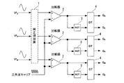
- a two-arm modulation method that lowers the switching frequency while minimizing a decrease in waveform control performance is conventionally known. This is because the switching of one phase semiconductor switch element is performed by correcting the voltage command value of each phase so that the voltage command value of one phase among the voltage command values of three phases is equal to or greater than the amplitude value of the triangular wave carrier. This is a method of stopping for a certain period and lowering the average switching frequency in the three phases (Patent Document 1).
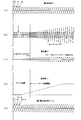
- FIG. 13 is a time chart of a three-phase voltage command value and a triangular wave carrier in the two-arm modulation method
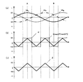
- FIG. 14A is a time chart of a three-phase voltage command value in the three-arm modulation method
- FIG. 14C shows a time chart of the voltage command value in the two-arm modulation method.
- the modulation factor of the voltage command value of each phase is m.
- the voltage command value V * U becomes the maximum value in the A section
- the voltage command value V * W Becomes the minimum value in the B section.
- the quantity ⁇ (the waveform in FIG. 14B) may be added to the three-phase voltage command values V * U , V * V , and V * W , respectively.
- the voltage command value of any one phase is always the amplitude of the triangular wave carrier every 60 ° interval, as in the waveforms of V * U + ⁇ , V * V + ⁇ , V * W + ⁇ shown in FIG.
- the semiconductor switch element stops switching.
- W + ⁇ can be generated.
- Patent Document 2 discloses a motor control device that switches between a 2-arm modulation system and a 3-arm modulation system.
- JP 59-139871 A JP 2007-151344 (paragraphs [0056] to [0065], FIG. 2, FIG. 4, FIG. 5)
- the two-arm modulation method is more efficient, but has the following problems.
- the other two phases for example, the V phase and the W phase
- the other two phases are switched during the period when the switching of the semiconductor switch element of one phase (for example, the U phase) is suspended. Since the amplitude of the voltage command value increases, the fine pulse width to the gate signal G U (i.e., on-duty 10% or less) period is observed.
- a dead time is provided in the gate signal in order to avoid that the semiconductor switch elements of the upper and lower arms of the same phase are turned on at the same time, and the timing at which the semiconductor switch element is switched on and off is delayed.
- the modulation factor m is further reduced, a period in which the pulse width (on duty) of the gate signal is further reduced occurs, so that the dead time is provided and the on / off operation cannot be performed. Voltage error may occur. For this reason, when the modulation factor m of the voltage command value is small, the voltage error is reduced by using the three-arm modulation method.
- the voltage accuracy is higher because the influence of the voltage error due to the dead time is less when the 2-arm modulation method is used than when the 3-arm modulation method is used.
- Efficiency is good because the average switching frequency is low.
- noise is a problem because the 2-arm modulation method has a lower average switching frequency than the 3-arm modulation method.
- Patent Document 2 switches the modulation method, it cannot solve the problem due to the difference in the modulation rate of the voltage command value as described above.
- a method for controlling a power conversion device is obtained by a gate signal generation unit that PWM modulates a voltage command value for a semiconductor switch element provided in a power conversion device that performs AC-DC conversion or DC-AC conversion.
- a method for controlling a power converter that outputs a received gate signal, wherein a voltage command value and a multiphase voltage that are maximum among the multiphase voltage command values in a correction term adder provided in the gate signal generation unit Compare the absolute value of the minimum voltage command value among the command values, and if the maximum voltage command value is larger, the signal obtained by subtracting the maximum voltage command value from the maximum value of the triangular wave carrier If the absolute value of the minimum voltage command value is larger, the signal corresponding to the signal generated by selecting the signal obtained by subtracting the minimum voltage command value from the minimum value of the triangular wave carrier is selected.
- a correction amount is calculated, and a triangular wave signal synchronized with the first correction amount is obtained by multiplying the signal obtained by adding the maximum voltage command value and the minimum voltage command value among the multiphase voltage command values by gain. Generate and calculate the corrected voltage command value by adding the second correction value generated by selecting the smaller of the triangular wave signal and the first correction value to the multiphase voltage command value.
- the gate signal obtained by PWM modulating the correction voltage command value is output to the semiconductor switch element.
- one aspect of the method for controlling the power conversion device according to the present invention is characterized in that the gain is variable according to a modulation rate of a voltage command value.
- the triangular wave signal synchronized with the first correction amount is a voltage command value that is the maximum and a voltage that is the minimum among the multiphase voltage command values.
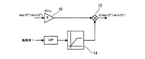
- a signal obtained by adding the command value is multiplied by the gain and the load factor of the power converter.
- one aspect of the method for controlling the power conversion device according to the present invention is characterized in that the load factor is a signal in which a harmonic component is attenuated by a low-pass filter and a time change rate is suppressed by a soft start circuit. To do.
- the three-arm modulation method is used when the modulation rate of the voltage command value is small, and the two-arm modulation is changed from the 3-arm modulation method as the modulation rate of the voltage command value increases. It is possible to change the modulation scheme continuously to the scheme.
- the present invention can combine the two-arm modulation method and the three-arm modulation method, noise can be reduced as compared with the case of only the two-arm modulation method. Furthermore, compared with the case where the simple change is made to the 3-arm modulation method when the voltage command value modulation rate is small, and the 2-arm modulation method is switched to when the voltage command value modulation rate is large, the sudden change in generated noise is suppressed. It becomes possible.
- the waveform is similar to that of the two-arm modulation method, so that a switching pause period can be generated and switching loss can be reduced.
- FIG. 3 is a configuration diagram illustrating an example of a gate signal generation unit in the first and second embodiments.
- FIG. 3 is a configuration diagram illustrating an example of a correction term adding unit 1 according to the first and second embodiments.
- 4 is a time chart showing an example of a signal waveform of each part of the correction term adding unit 1;
- 3 is a time chart showing an example of a voltage command value, k (max (V * ) + min (V * )), and correction amounts ⁇ and ⁇ in a three-arm modulation system.
- 5 is a time chart showing an example of each signal waveform when the modulation factor m of the voltage command value in the first embodiment is increased.
- FIG. 9 is a configuration diagram illustrating an example of a correction term addition unit 1 according to a third embodiment.
- FIG. 10 is a time chart showing an example of each signal waveform when the load factor l in the third embodiment is increased.
- FIG. 6 is a configuration diagram illustrating an example of a gain multiplier 10 and a load factor multiplier 13 according to a fourth embodiment.
- the time chart which shows an example of the voltage command value of a three-phase in a 2 arm modulation system, and a triangular wave carrier.
- the time chart which shows an example of the voltage command value in a 3 arm modulation system, the correction amount used for a 2 arm modulation system, and a 3 phase voltage command value.
- a power converter for example, a three-phase inverter
- Three-phase voltage command values V * U , V * V , and V * W are input to a gate signal generation unit that outputs signals.
- a second correction amount hereinafter referred to as a correction amount ⁇ is applied to the three-phase voltage command values V * U , V * V , and V * W as shown in FIG.
- a correction amount ⁇ a first correction amount for calculating the voltage command values V * U + ⁇ , V * V + ⁇ , and V * W + ⁇ of the two-arm modulation method.
- the maximum value calculator max (x, y, z) inputs the voltage command value V * U, V * V, V * W, the voltage command value V * U, V * V, from among the V * W
- the maximum value max (V * ) selected from the maximum voltage command value is output.
- the minimum value calculator min (x, y, z) inputs voltage command values V * U , V * V , V * W , and the voltage command values V * U , V * V , V * W are inputted.
- a minimum value min (V * ) is selected by selecting the minimum voltage command value from the inside.
- the comparator 5 compares the maximum value max (V * ) with the absolute value
- , s1 1, and if the absolute value
- is larger than the maximum value max (V * ), a signal s1 that outputs s1 0 is output to the switch 6, 6 is used for determination.
- the maximum value max (V * ) and the minimum value min (V * ) output from the maximum value calculator max (x, y, z) and the minimum value calculator min (x, y, z) are subtractors. 7 and 8, respectively, 1-max (V * ) and -1-min (V * ) are calculated in the subtracters 7 and 8, and the signals are output to the switch 6.
- the waveform of the correction amount ⁇ output from the switch 6 corresponds to the waveform of the correction amount ⁇ used in the two-arm modulation method shown in FIG.
- the calculation method of the correction amount ⁇ described here is an example, and the correction amount ⁇ may be calculated by other calculation methods.
- the maximum value max (V * ) output from the maximum value calculator max (x, y, z) and the minimum value min (V * ) output from the minimum value calculator min (x, y, z). are added by the adder 9.
- the added max (V * ) + min (V * ) signal is multiplied by the gain k in the gain multiplier 10 and output as a k (max (V * ) + min (V * )) signal.
- is input to the comparator 11. Then, the comparator 11 compares the absolute value
- the correction amount ⁇ output from the switch 6 and the k (max (V * ) + min (V * )) signal output from the gain multiplier 10 are input to the switch 12, and the switch 12 is output from the comparator 11.
- the signal output from the switch 12 is added to the three-phase voltage command values V * U , V * V , and V * W , respectively, as the correction amount ⁇ used in the modulation method of the first embodiment, and the correction voltage command
- the values V * U + ⁇ , V * V + ⁇ , and V * W + ⁇ are calculated. The above is the principle of correcting the voltage command value in the first embodiment.
- correction term addition unit 1 in FIG. 2 will be described based on a time chart showing an example of a signal waveform of each part of the correction term addition unit 1 in FIG.
- FIG. 3A is a time chart showing an example of three-phase voltage command values V * U , V * V , and V * W when the modulation factor is m.
- the voltage command values V * U , V * V , and V * W are obtained as shown in FIG. 3B by the maximum value calculator max (x, y, z) and the minimum value calculator min (x, y, z).
- a maximum value max (V * ) and a minimum value min (V * ) as shown in the chart are calculated.
- the comparator 5 compares the maximum value max (V * ) with the absolute value
- the signal s1 output from the comparator 5 has a maximum period max (V * ) greater than the absolute value
- is greater than the maximum value max (V * ), s1 0.
- the max (V * ) + min (V * ) signal output from the adder 9 has a triangular waveform synchronized with the correction amount ⁇ as shown in FIG.
- the k (max (V * ) + min (V * )) signal multiplied by the gain k in the gain multiplier 10 is also a signal having a waveform synchronized with the correction amount ⁇ .
- the signal s2 output from the comparator 11 has an absolute value
- . S2 0.
- k (max (V * ) + min (V * )) and the correction amount ⁇ have waveforms shown in FIG.
- a correction amount ⁇ is output.
- the correction term adding unit 1 shown in FIG. 1 may be configured as shown in FIG. 2, and a gate signal may be generated by a triangular wave comparison to turn on and off the switch element.
- a time chart of ⁇ is shown.
- the U-phase voltage command value V * U in FIG. 4A is taken as an example, and at the point A that is the maximum value, k (max (V * ) + min ( V * )) signal also has a maximum value, and the value is obtained by the following equation (1).
- the value of the correction amount ⁇ at the point A can be obtained by the following equation (2).
- the correction amount ⁇ shown in FIG. 4C is output by selecting the smaller absolute value of k (max (V * ) + min (V * )) and the correction amount ⁇ in the switch 12.
- FIG. 5A shows a time chart of the U-phase voltage command value V * U when the modulation factor m is increased from 0 to 1.15 with a constant slope
- FIG. 5B shows the correction amounts ⁇ and k (max (V * ) + min (V * )) signal time chart
- FIG. 5 (c) shows the correction amount ⁇ time chart
- FIG. 5 (d) shows the U-phase correction voltage command value V * U + ⁇ of the first embodiment.
- the correction amount ⁇ and the k (max (V * ) + min (V * )) signal are zero cross and k ( It becomes equal in the point which becomes the maximum value or the minimum value of max (V * ) + min (V * )). Therefore, when the smaller absolute value of the correction amount ⁇ and k (max (V * ) + min (V * )) is selected as the correction amount ⁇ , the correction amount ⁇ is k (max (V * ) + min (V * ) . )) Is selected.
- the absolute value of the maximum value or the minimum value of the k (max (V * ) + min (V * )) signal is larger than the absolute value of the correction amount ⁇ . Therefore, if the smaller of the absolute values of the correction amount ⁇ and the k (max (V * ) + min (V * )) signal is selected, the correction amount ⁇ and k ( max (V * ) + min (V * )) signals are mixed.
- the ratio of the correction amount ⁇ used in the two-arm modulation method increases as the correction amount ⁇ .
- the correction amount ⁇ increases. All the selected signals have a correction amount ⁇ , and the modulation method is completely the two-arm modulation method.
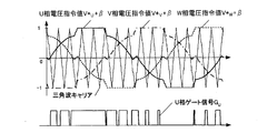
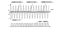
- FIG. 6 shows correction voltage command values V * U + ⁇ , V * V + ⁇ , V * W + ⁇ , and U-phase gate when the modulation method of the first embodiment is used when the modulation factor m of the voltage command value is 0.1.
- the three-arm modulation method is used when the modulation factor m of the voltage command value is small, and the three-arm modulation is performed as the modulation factor m of the voltage command value increases. It is possible to continuously change the modulation method from the method to the two-arm modulation method.
- the modulation system of the first embodiment combines the 2-arm modulation system and the 3-arm modulation system, it is possible to reduce noise compared to the case of only the 2-arm modulation system. Furthermore, when the modulation rate m of the voltage command value is small, the 3-arm modulation method is adopted, and when the modulation rate m of the voltage command value is large, the generated noise is smaller than when the 2-arm modulation method is adopted. It is possible to suppress sudden changes.
- the gate signal has a waveform similar to that of the two-arm modulation method, and a switching pause period occurs, so that switching loss can be reduced.
- phase voltage command values are converted into polar coordinates, phase and amplitude information is obtained, and a complicated calculation such as calculation of the modulation method is not used, and a simple analog circuit or a simple digital circuit such as an FPGA can be used. Corrections can be made directly from the phase voltage command values V * U , V * V , and V * W.
- the correction amount ⁇ is added to the three-phase voltage command values V * U , V * V , and V * W , and corrected by changing the zero-phase voltage (that is, the ground voltage). Yes.
- the gain k in the modulation scheme of the first embodiment is made variable according to the modulation factor m.
- FIG. 8A shows a time chart of the U-phase voltage command value V * U when the modulation factor m is increased from 0 to 1.15 with a constant slope
- FIG. 8B shows the correction amounts ⁇ and k (max (V * ) + min (V * )) signal time chart
- FIG. 8C shows the gain k time chart
- FIG. 8D shows the correction amount ⁇ time chart
- FIG. 8E shows the second embodiment. 4 shows a time chart of the U-phase correction voltage command value V * U + ⁇ .
- k is increased with a constant slope.
- the gain k is assumed to be constant.
- the amplitude value of the correction amount ⁇ can be suppressed more than in the first embodiment, and the leakage current can be reduced.
- the ratio between the three-arm modulation method and the two-arm modulation method is changed depending on the magnitude of the modulation factor m.
- the third embodiment not only the modulation factor m but also the modulation factor m and the load factor of the power converter.
- the ratio between the three-arm modulation method and the two-arm modulation method is changed according to l.
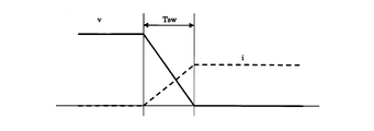
- FIG. 9 is an explanatory diagram of the switching loss. Furthermore, loss w SW per switching to the following equation (5) shows the switching loss W SW per unit time in the following equation (6).
- the voltage v and the current i change linearly as shown in FIG.
- the energy w SW of loss during switching losses T SW becomes equation (5). Further, as represented by the above equation (6), the switching loss W SW per unit time is proportional to the current i. Therefore, when the load factor l is low and the current i flowing through the semiconductor switch element is small, the switching loss W SW is not a problem.
- the switching loss W SW when the load factor l is high and the current i flowing through the semiconductor switch element is large, the switching loss W SW also increases accordingly. Therefore, since the switching loss W SW does not become a problem during the period when the load factor l is low, noise and harmonic components are reduced as a three-arm modulation method, and the switching loss W SW as a two-arm modulation method when the load factor l is high.
- FIG. 10 is a configuration diagram illustrating an example of the correction term adding unit 1 according to the third embodiment.
- the corrected voltage command value V * U + ⁇ by adding the operation amount ⁇ considering the load factor l to the voltage command values V * U , V * V , V * W.
- V * V + ⁇ and V * W + ⁇ are generated.
- the load factor multiplier 13 multiplies the k (max (V * ) + min (V * )) signal output from the gain multiplier 10 by the load factor l of the power converter, and k1 ( A max (V * ) + min (V * )) signal is calculated.
- the kl (max (V * ) + min (V * )) signal is a signal added to give a gradient to a steep change in voltage which is a problem in the two-arm modulation method.
- kl (max (V * ) + min (V) is input to one input terminal of the comparator 11. * ))
- the switch 12 receives the kl (max (V * ) + min (V * )) signal calculated by the load factor multiplier 13.
- the correction amount ⁇ is generated by selecting the smaller of the correction amount ⁇ and the absolute value of the kl (max (V * ) + min (V * )) signal in the switch 12.
- the switch 12 is switched by comparing the correction amount ⁇ with the absolute value of the kl (max (V * ) + min (V * )) signal, and
- FIG. 11A shows a time chart of the voltage command values V * U , V * V , and V * W
- FIG. 11B shows the time of the correction amount ⁇ and the kl (max (V * ) + min (V * )) signal
- FIG. 11C is a time chart of the correction amount ⁇
- FIG. 11D is a time chart of the load factor l
- FIG. 11E is a correction voltage command value V * U + ⁇ , V * of the third embodiment .
- the time chart of V + ⁇ and V * W + ⁇ is shown.
- the correction amount ⁇ shown in FIG. 11C is a signal generated by selecting the smaller of the correction amount ⁇ and the absolute value of the kl (max (V * ) + min (V * )) signal. Therefore, when the correction amount ⁇ and the smaller absolute value of the kl (max (V * ) + min (V * )) signal are selected as the correction amount ⁇ , the period during which the load factor l is small is kl (max (V * ) + min. Only the (V * )) signal is selected.
- the absolute value of the maximum value or the minimum value of the kl (max (V * ) + min (V * )) signal is larger than the absolute value of the correction amount ⁇ . Therefore, when the correction amount ⁇ and the smaller absolute value of the kl (max (V * ) + min (V * )) signal are selected as the correction amount ⁇ , the correction amounts ⁇ and kl (max (V * ) used in the two-arm modulation method are selected . ) + Min (V * )) signal.
- the three-arm modulation method and the load factor l are It is possible to switch between the 3-arm modulation method and the 2-arm modulation method according to the load factor l as in the 2-arm modulation method during a large period.
- the switching loss W SW is also small during the period when the load factor l is low, it is possible to reduce the noise and harmonic components by using three-arm modulation. Further, when the load factor 1 is large, the two-arm modulation is used, and the switching loss W SW can be reduced.
- the third embodiment may be applied to a power conversion device such as a solar PCS in which the load factor l changes gradually.
- a power conversion device such as a solar PCS in which the load factor l changes gradually.
- the load factor l is simply multiplied by the k (max (V * ) + min (V * )) signal.
- the load factor l increases rapidly when a power failure occurs.
- the control method of the third embodiment is used for the power conversion device in which the load factor l changes abruptly, when the load factor l changes suddenly, the three-arm modulation method is suddenly switched. As a result, a strong stress is given to the apparatus.
- the load factor 1 is output to the load factor multiplier 13 via the low-pass filter LPF and the soft start circuit 14, and k (max (V * ) + min (V * ) . )) Multiply the signal. Since other configurations are the same as those of the third embodiment, the description thereof is omitted.
- the low-pass filter LPF attenuates the harmonic component contained in the load factor l and outputs only the fundamental wave component of the load factor l. Further, the soft start circuit 14 suppresses the time change rate of the output below a predetermined value and gradually increases the output.
- the fourth embodiment may be applied to, for example, an uninterruptible power supply device or a voltage sag compensator with a sudden change in the load factor l.
- the method of correcting the three-phase voltage command value has been described.
- the voltage command value can be applied to a multi-phase of three or more phases.
- V * U, V * V, V * W ... voltage command value G U, G V, G W , G X, G Y, G Z ... gate signal alpha, beta ... correction amount k ... Gain max (V * ): Maximum value of voltage command value min (V * ): Minimum value of voltage command value
Landscapes
- Engineering & Computer Science (AREA)
- Power Engineering (AREA)
- Inverter Devices (AREA)
- Rectifiers (AREA)
- Ac-Ac Conversion (AREA)
Abstract
Description


[実施形態2]
[実施形態3]


[実施形態4]
V* U,V* V,V* W…電圧指令値
GU,GV,GW,GX,GY,GZ…ゲート信号
α,β…補正量
k…ゲイン
max(V*)…電圧指令値の最大値
min(V*)…電圧指令値の最小値
Claims (4)
- 交流‐直流変換あるいは直流‐交流変換を行う電力変換装置に備えられた半導体スイッチ素子に対して、電圧指令値をPWM変調するゲート信号生成部により得られたゲート信号を出力する電力変換装置の制御方法であって、
ゲート信号生成部に備えられた補正項加算部において、
多相の電圧指令値のうち最大となる電圧指令値と多相の電圧指令値のうち最小となる電圧指令値の絶対値とを比較し、
前記最大となる電圧指令値の方が大きい場合は、三角波キャリアの最大値から前記最大となる電圧指令値を減算した信号を選択し、
前記最小となる電圧指令値の絶対値の方が大きい場合は、三角波キャリアの最小値から前記最小となる電圧指令値を減算した信号を選択して生成した信号に相当する第一補正量を演算し、
多相の電圧指令値のうち最大となる電圧指令値と最小となる電圧指令値を加算した信号にゲインを乗算して前記第一補正量と同期した三角波状の信号を生成し、
この三角波状の信号と第一補正量とのうち絶対値の小さい方を選択して生成した第二補正量を多相の電圧指令値にそれぞれ加算して補正電圧指令値を演算し、
この補正電圧指令値をPWM変調して得られたゲート信号を前記半導体スイッチ素子に出力することを特徴とする電力変換装置の制御方法。 - 前記ゲインは、電圧指令値の変調率に応じて可変とすることを特徴とする請求項1記載の電力変換装置の制御方法。
- 前記第一補正量と同期した三角波状の信号は、
多相の電圧指令値のうち最大となる電圧指令値と最小となる電圧指令値を加算した信号に、ゲインと電力変換装置の負荷率を乗算した値とすることを特徴とする請求項1または2記載の電力変換装置の制御方法。 - 前記負荷率は、
ローパスフィルタによって高調波成分が減衰され、
ソフトスタート回路によって時間変化率が抑制された信号とすることを特徴とする請求項3記載の電力変換装置の制御方法。
Priority Applications (6)
| Application Number | Priority Date | Filing Date | Title |
|---|---|---|---|
| JP2011509352A JP5304891B2 (ja) | 2009-04-16 | 2010-04-15 | 電力変換装置の制御方法 |
| US13/264,592 US8659918B2 (en) | 2009-04-16 | 2010-04-15 | Method of controlling power conversion device |
| CN201080016973.4A CN102396142B (zh) | 2009-04-16 | 2010-04-15 | 控制电力变换设备的方法 |
| EP10764511.1A EP2413488A4 (en) | 2009-04-16 | 2010-04-15 | Method of controlling power conversion device |
| KR1020117025188A KR101266278B1 (ko) | 2009-04-16 | 2010-04-15 | 전력변환장치의 제어방법 |
| SG2011074465A SG175197A1 (en) | 2009-04-16 | 2010-04-15 | Method of controlling power conversion device |
Applications Claiming Priority (2)
| Application Number | Priority Date | Filing Date | Title |
|---|---|---|---|
| JP2009-099491 | 2009-04-16 | ||
| JP2009099491 | 2009-04-16 |
Publications (1)
| Publication Number | Publication Date |
|---|---|
| WO2010119929A1 true WO2010119929A1 (ja) | 2010-10-21 |
Family
ID=42982586
Family Applications (1)
| Application Number | Title | Priority Date | Filing Date |
|---|---|---|---|
| PCT/JP2010/056786 WO2010119929A1 (ja) | 2009-04-16 | 2010-04-15 | 電力変換装置の制御方法 |
Country Status (7)
| Country | Link |
|---|---|
| US (1) | US8659918B2 (ja) |
| EP (1) | EP2413488A4 (ja) |
| JP (1) | JP5304891B2 (ja) |
| KR (1) | KR101266278B1 (ja) |
| CN (1) | CN102396142B (ja) |
| SG (1) | SG175197A1 (ja) |
| WO (1) | WO2010119929A1 (ja) |
Cited By (3)
| Publication number | Priority date | Publication date | Assignee | Title |
|---|---|---|---|---|
| FR2971649A1 (fr) * | 2011-02-16 | 2012-08-17 | Mitsubishi Electric Corp | Onduleur de puissance et dispositif de commande de direction assistee electrique |
| WO2014141398A1 (ja) * | 2013-03-13 | 2014-09-18 | 株式会社日立製作所 | Pwm制御方法とそれを用いた電力変換装置 |
| JP7202244B2 (ja) | 2019-04-03 | 2023-01-11 | オリエンタルモーター株式会社 | 電力変換装置 |
Families Citing this family (7)
| Publication number | Priority date | Publication date | Assignee | Title |
|---|---|---|---|---|
| CN107112936B (zh) * | 2014-12-08 | 2019-08-16 | 株式会社日立产机系统 | 电力转换装置和电力转换装置的控制方法 |
| WO2017168522A1 (ja) * | 2016-03-28 | 2017-10-05 | 三菱電機株式会社 | 電力変換装置 |
| JP6361803B1 (ja) * | 2017-07-27 | 2018-07-25 | 株式会社明電舎 | マルチレベルインバータの制御装置および制御方法 |
| US10541626B1 (en) | 2019-01-15 | 2020-01-21 | Rockwell Automation Technologies, Inc. | Power conversion system with PWM carrier emulation |
| US10601343B1 (en) | 2019-01-16 | 2020-03-24 | Rockwell Automation Technologies, Inc. | Power conversion system with PWM carrier transition smoothing and autotuning |
| CN110071680B (zh) * | 2019-05-14 | 2021-05-14 | 深圳市正弦电气股份有限公司 | 一种减小变频器温升的pwm调制方法及系统 |
| US11336206B2 (en) | 2020-09-23 | 2022-05-17 | Rockwell Automation Technoligies, Inc. | Switching frequency and PWM control to extend power converter lifetime |
Citations (7)
| Publication number | Priority date | Publication date | Assignee | Title |
|---|---|---|---|---|
| JPS59139871A (ja) | 1983-01-26 | 1984-08-10 | Sharp Corp | ブリツジ形3相正弦波インバ−タのパルス幅変調方式 |
| JPS63290170A (ja) * | 1987-05-20 | 1988-11-28 | Mitsubishi Electric Corp | Pwmインバ−タ装置 |
| JPH01274669A (ja) * | 1988-04-27 | 1989-11-02 | Fuji Electric Co Ltd | 三相電圧形インバータのpwm制御方法 |
| JPH05199796A (ja) * | 1992-01-17 | 1993-08-06 | Meidensha Corp | 可変速駆動装置の電流制御方式 |
| WO2001065675A1 (fr) * | 2000-02-28 | 2001-09-07 | Kabushiki Kaisha Yaskawa Denki | Procede de commande d'impulsion de modulation de largeur d'impulsion (pwm) |
| JP2004048885A (ja) * | 2002-07-10 | 2004-02-12 | Mitsubishi Electric Corp | 電力変換装置 |
| JP2007151344A (ja) | 2005-11-29 | 2007-06-14 | Denso Corp | 磁極位置推定方法、モータ速度推定方法及びモータ制御装置 |
Family Cites Families (9)
| Publication number | Priority date | Publication date | Assignee | Title |
|---|---|---|---|---|
| WO1995002921A1 (fr) * | 1992-01-17 | 1995-01-26 | Kabushiki Kaisha Meidensha | Appareil et procede de regulation du courant d'un entrainement a vitesse variable |
| US5610806A (en) * | 1995-06-19 | 1997-03-11 | Allen-Bradley Company, Inc. | Pulse width modulation method for driving three phase power inverter/converter switches with balanced discontinuous phase commands |
| KR100240953B1 (ko) * | 1996-10-02 | 2000-01-15 | 이종수 | 전력변환장치의 펄스폭 변조 방법 |
| US6324085B2 (en) * | 1999-12-27 | 2001-11-27 | Denso Corporation | Power converter apparatus and related method |
| JP4045105B2 (ja) * | 2002-01-30 | 2008-02-13 | 株式会社日立産機システム | パルス幅変調方法、電力変換装置、およびインバータ装置 |
| JP4491434B2 (ja) * | 2006-05-29 | 2010-06-30 | トヨタ自動車株式会社 | 電力制御装置およびそれを備えた車両 |
| DE102008054487A1 (de) * | 2008-01-09 | 2009-07-16 | DENSO CORPORARTION, Kariya-shi | Steuersystem für eine mehrphasige elektrische Drehmaschine |
| JP4729054B2 (ja) * | 2008-01-28 | 2011-07-20 | 株式会社東芝 | 通信用半導体集積回路 |
| TWI410037B (zh) * | 2008-12-08 | 2013-09-21 | Ind Tech Res Inst | 電源轉換裝置及其控制方法 |
-
2010
- 2010-04-15 EP EP10764511.1A patent/EP2413488A4/en not_active Withdrawn
- 2010-04-15 WO PCT/JP2010/056786 patent/WO2010119929A1/ja active Application Filing
- 2010-04-15 KR KR1020117025188A patent/KR101266278B1/ko not_active IP Right Cessation
- 2010-04-15 JP JP2011509352A patent/JP5304891B2/ja active Active
- 2010-04-15 US US13/264,592 patent/US8659918B2/en not_active Expired - Fee Related
- 2010-04-15 CN CN201080016973.4A patent/CN102396142B/zh not_active Expired - Fee Related
- 2010-04-15 SG SG2011074465A patent/SG175197A1/en unknown
Patent Citations (7)
| Publication number | Priority date | Publication date | Assignee | Title |
|---|---|---|---|---|
| JPS59139871A (ja) | 1983-01-26 | 1984-08-10 | Sharp Corp | ブリツジ形3相正弦波インバ−タのパルス幅変調方式 |
| JPS63290170A (ja) * | 1987-05-20 | 1988-11-28 | Mitsubishi Electric Corp | Pwmインバ−タ装置 |
| JPH01274669A (ja) * | 1988-04-27 | 1989-11-02 | Fuji Electric Co Ltd | 三相電圧形インバータのpwm制御方法 |
| JPH05199796A (ja) * | 1992-01-17 | 1993-08-06 | Meidensha Corp | 可変速駆動装置の電流制御方式 |
| WO2001065675A1 (fr) * | 2000-02-28 | 2001-09-07 | Kabushiki Kaisha Yaskawa Denki | Procede de commande d'impulsion de modulation de largeur d'impulsion (pwm) |
| JP2004048885A (ja) * | 2002-07-10 | 2004-02-12 | Mitsubishi Electric Corp | 電力変換装置 |
| JP2007151344A (ja) | 2005-11-29 | 2007-06-14 | Denso Corp | 磁極位置推定方法、モータ速度推定方法及びモータ制御装置 |
Non-Patent Citations (1)
| Title |
|---|
| See also references of EP2413488A4 * |
Cited By (4)
| Publication number | Priority date | Publication date | Assignee | Title |
|---|---|---|---|---|
| FR2971649A1 (fr) * | 2011-02-16 | 2012-08-17 | Mitsubishi Electric Corp | Onduleur de puissance et dispositif de commande de direction assistee electrique |
| US8917050B2 (en) | 2011-02-16 | 2014-12-23 | Mitsubishi Electric Corporation | Power inverter and electric power steering controller |
| WO2014141398A1 (ja) * | 2013-03-13 | 2014-09-18 | 株式会社日立製作所 | Pwm制御方法とそれを用いた電力変換装置 |
| JP7202244B2 (ja) | 2019-04-03 | 2023-01-11 | オリエンタルモーター株式会社 | 電力変換装置 |
Also Published As
| Publication number | Publication date |
|---|---|
| KR20110137378A (ko) | 2011-12-22 |
| JP5304891B2 (ja) | 2013-10-02 |
| SG175197A1 (en) | 2011-11-28 |
| KR101266278B1 (ko) | 2013-05-22 |
| US20120033470A1 (en) | 2012-02-09 |
| EP2413488A4 (en) | 2017-08-16 |
| JPWO2010119929A1 (ja) | 2012-10-22 |
| CN102396142A (zh) | 2012-03-28 |
| EP2413488A1 (en) | 2012-02-01 |
| US8659918B2 (en) | 2014-02-25 |
| CN102396142B (zh) | 2014-04-30 |
Similar Documents
| Publication | Publication Date | Title |
|---|---|---|
| JP5304891B2 (ja) | 電力変換装置の制御方法 | |
| US9882466B2 (en) | Power conversion device including an AC/DC converter and a DC/DC converter | |
| EP2798731B1 (en) | A system, a method and a computer program product for controlling electric power supply | |
| US8649195B2 (en) | Hybrid space vector PWM schemes for interleaved three-phase converters | |
| KR102009509B1 (ko) | 3상 인버터의 옵셋 전압 생성 장치 및 방법 | |
| KR101621994B1 (ko) | 회생형 고압 인버터의 제어장치 | |
| US20190222135A1 (en) | Control device for direct power converter | |
| KR102009512B1 (ko) | 3상 인버터의 옵셋 전압 생성 장치 및 방법 | |
| US20130181654A1 (en) | Motor drive system employing an active rectifier | |
| US9350227B2 (en) | Power converter control method | |
| JP4929863B2 (ja) | 電力変換装置 | |
| Jabbarnejad et al. | Combined control of grid connected converters based on a flexible switching table for fast dynamic and reduced harmonics | |
| Zeng et al. | Improved current controller based on SVPWM for three-phase grid-connected voltage source inverters | |
| KR102416374B1 (ko) | 고압인버터 전력셀의 직류단 전압 제어장치 | |
| JP7367662B2 (ja) | 電力変換装置および電力変換装置の制御方法 | |
| JPWO2019097835A1 (ja) | 電力変換装置 | |
| Adzic et al. | Space vector modulated three-phase current source converter for dc motor drive | |
| JP7202244B2 (ja) | 電力変換装置 | |
| JP5428744B2 (ja) | 電力変換装置の制御方法 | |
| Nammalvar et al. | A Novel Three Phase Hybrid Unidirectional Rectifier for High Power Factor Applications | |
| JP2011172387A (ja) | 電力変換制御装置、コンバータ制御回路、電力変換制御方法、電力変換制御用プログラム及び記録媒体 | |
| WO2023214462A1 (ja) | 電力変換装置 | |
| KR101852015B1 (ko) | 하이브리드 비례 적분 제어기 및 그 제어기를 갖는 인버터 시스템 | |
| JP2006020417A (ja) | 電力変換装置の制御装置及び方法 | |
| Smith et al. | Improved STATCOM Performance using Modulated Finite Control Set Model Predictive Control |
Legal Events
| Date | Code | Title | Description |
|---|---|---|---|
| WWE | Wipo information: entry into national phase |
Ref document number: 201080016973.4 Country of ref document: CN |
|
| 121 | Ep: the epo has been informed by wipo that ep was designated in this application |
Ref document number: 10764511 Country of ref document: EP Kind code of ref document: A1 |
|
| WWE | Wipo information: entry into national phase |
Ref document number: 2011509352 Country of ref document: JP |
|
| WWE | Wipo information: entry into national phase |
Ref document number: 13264592 Country of ref document: US |
|
| NENP | Non-entry into the national phase |
Ref country code: DE |
|
| ENP | Entry into the national phase |
Ref document number: 20117025188 Country of ref document: KR Kind code of ref document: A |
|
| WWE | Wipo information: entry into national phase |
Ref document number: 2010764511 Country of ref document: EP |
|
| WWE | Wipo information: entry into national phase |
Ref document number: 4573/KOLNP/2011 Country of ref document: IN |