EP2400568A2 - Light emitting device package including several lenses and lighting system - Google Patents
Light emitting device package including several lenses and lighting system Download PDFInfo
- Publication number
- EP2400568A2 EP2400568A2 EP11167966A EP11167966A EP2400568A2 EP 2400568 A2 EP2400568 A2 EP 2400568A2 EP 11167966 A EP11167966 A EP 11167966A EP 11167966 A EP11167966 A EP 11167966A EP 2400568 A2 EP2400568 A2 EP 2400568A2
- Authority
- EP
- European Patent Office
- Prior art keywords
- light emitting
- emitting device
- device package
- light
- lens
- Prior art date
- Legal status (The legal status is an assumption and is not a legal conclusion. Google has not performed a legal analysis and makes no representation as to the accuracy of the status listed.)
- Granted
Links
Images





Classifications
-
- H—ELECTRICITY
- H10—SEMICONDUCTOR DEVICES; ELECTRIC SOLID-STATE DEVICES NOT OTHERWISE PROVIDED FOR
- H10H—INORGANIC LIGHT-EMITTING SEMICONDUCTOR DEVICES HAVING POTENTIAL BARRIERS
- H10H20/00—Individual inorganic light-emitting semiconductor devices having potential barriers, e.g. light-emitting diodes [LED]
- H10H20/80—Constructional details
- H10H20/85—Packages
- H10H20/855—Optical field-shaping means, e.g. lenses
-
- F—MECHANICAL ENGINEERING; LIGHTING; HEATING; WEAPONS; BLASTING
- F21—LIGHTING
- F21K—NON-ELECTRIC LIGHT SOURCES USING LUMINESCENCE; LIGHT SOURCES USING ELECTROCHEMILUMINESCENCE; LIGHT SOURCES USING CHARGES OF COMBUSTIBLE MATERIAL; LIGHT SOURCES USING SEMICONDUCTOR DEVICES AS LIGHT-GENERATING ELEMENTS; LIGHT SOURCES NOT OTHERWISE PROVIDED FOR
- F21K9/00—Light sources using semiconductor devices as light-generating elements, e.g. using light-emitting diodes [LED] or lasers
- F21K9/20—Light sources comprising attachment means
- F21K9/23—Retrofit light sources for lighting devices with a single fitting for each light source, e.g. for substitution of incandescent lamps with bayonet or threaded fittings
-
- F—MECHANICAL ENGINEERING; LIGHTING; HEATING; WEAPONS; BLASTING
- F21—LIGHTING
- F21Y—INDEXING SCHEME ASSOCIATED WITH SUBCLASSES F21K, F21L, F21S and F21V, RELATING TO THE FORM OR THE KIND OF THE LIGHT SOURCES OR OF THE COLOUR OF THE LIGHT EMITTED
- F21Y2115/00—Light-generating elements of semiconductor light sources
- F21Y2115/10—Light-emitting diodes [LED]
-
- H—ELECTRICITY
- H10—SEMICONDUCTOR DEVICES; ELECTRIC SOLID-STATE DEVICES NOT OTHERWISE PROVIDED FOR
- H10H—INORGANIC LIGHT-EMITTING SEMICONDUCTOR DEVICES HAVING POTENTIAL BARRIERS
- H10H20/00—Individual inorganic light-emitting semiconductor devices having potential barriers, e.g. light-emitting diodes [LED]
- H10H20/80—Constructional details
- H10H20/85—Packages
- H10H20/852—Encapsulations
- H10H20/853—Encapsulations characterised by their shape
-
- H—ELECTRICITY
- H10—SEMICONDUCTOR DEVICES; ELECTRIC SOLID-STATE DEVICES NOT OTHERWISE PROVIDED FOR
- H10W—GENERIC PACKAGES, INTERCONNECTIONS, CONNECTORS OR OTHER CONSTRUCTIONAL DETAILS OF DEVICES COVERED BY CLASS H10
- H10W74/00—Encapsulations, e.g. protective coatings
-
- H—ELECTRICITY
- H10—SEMICONDUCTOR DEVICES; ELECTRIC SOLID-STATE DEVICES NOT OTHERWISE PROVIDED FOR
- H10W—GENERIC PACKAGES, INTERCONNECTIONS, CONNECTORS OR OTHER CONSTRUCTIONAL DETAILS OF DEVICES COVERED BY CLASS H10
- H10W74/00—Encapsulations, e.g. protective coatings
- H10W74/10—Encapsulations, e.g. protective coatings characterised by their shape or disposition
-
- H—ELECTRICITY
- H10—SEMICONDUCTOR DEVICES; ELECTRIC SOLID-STATE DEVICES NOT OTHERWISE PROVIDED FOR
- H10W—GENERIC PACKAGES, INTERCONNECTIONS, CONNECTORS OR OTHER CONSTRUCTIONAL DETAILS OF DEVICES COVERED BY CLASS H10
- H10W90/00—Package configurations
-
- H—ELECTRICITY
- H10—SEMICONDUCTOR DEVICES; ELECTRIC SOLID-STATE DEVICES NOT OTHERWISE PROVIDED FOR
- H10W—GENERIC PACKAGES, INTERCONNECTIONS, CONNECTORS OR OTHER CONSTRUCTIONAL DETAILS OF DEVICES COVERED BY CLASS H10
- H10W90/00—Package configurations
- H10W90/701—Package configurations characterised by the relative positions of pads or connectors relative to package parts
- H10W90/751—Package configurations characterised by the relative positions of pads or connectors relative to package parts of bond wires
- H10W90/756—Package configurations characterised by the relative positions of pads or connectors relative to package parts of bond wires between a chip and a stacked lead frame, conducting package substrate or heat sink
Definitions
- the embodiment relates to a light emitting device package and a lighting system.
- LEDs Light emitting diodes
- LEDs are a kind of semiconductor devices that convert electric energy into light.
- the LED is advantageous as compared with conventional light sources, such as a fluorescent lamp or a glow lamp, in terms of power consumption, life span, response speed, safety and environmental-friendly requirement.
- the LEDs are increasingly used as light sources for lighting devices such as various lamps, liquid crystal displays, electric signboards, and street lamps.
- the embodiment provides a light emitting device package capable of improving light efficiency and a lighting system having the light emitting device package.
- the embodiment provides a light emitting device package capable of uniformly discharging light and a lighting system having the light emitting device package.
- a light emitting device package comprises a body comprising a recess and a plurality of light emitting device receiving parts formed in a bottom surface of the recess, a plurality of light emitting devices separately positioned in the light emitting device receiving parts, a plurality of individual lenses spaced apart from each other on the light emitting device receiving parts, and a common lens covering the individual lenses.
- a lighting system comprises a board, and a light emitting module comprising a light emitting device package provided on the board.
- the light emitting device comprises a body comprising a recess and a plurality of light emitting device receiving parts formed in a bottom surface of the recess, a plurality of light emitting devices separately positioned in the light emitting device receiving parts, a plurality of individual lenses spaced apart from each other on the light emitting device receiving parts, and a common lens covering the individual lenses.
- the receiving parts, the resin members, and individual lenses are provided corresponding to each of light emitting devices. Therefore, since the individual lenses can have a structure suitable for light efficiency, the efficiency of the light emitting device package can be improved.
- the common lens having a refractive index lower than that of the individual lenses is additionally provided, so that efficiency can be more improved.
- the resin members may comprise different luminescence materials, or the individual lenses may have different shapes and different characteristics. Therefore, various light emitting device packages can be manufactured suitably for desired characteristics. In particular, if the individual lenses have different curvatures or different refractive indexes based on the efficiency, a light can be uniformly discharged even in various types of the combination of light emitting devices and luminescence materials.
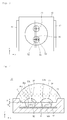
- FIG. 1 is a perspective view showing a light emitting device package according to a first embodiment
- FIG. 2 is a perspective view showing a light emitting device package of FIG. 1 without individual lenses, common lenses, and resin members;
- FIG. 3 is a plan view of FIG. 2 ;
- FIG. 4 is a sectional view taken along line IV-IV of FIG. 1 ;
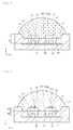
- FIG. 5 is a sectional view showing a light emitting device package according to a first modification of a first embodiment
- FIG. 6 is a sectional view showing a light emitting device package according to a second modification of the first embodiment
- FIG. 7 is a sectional view showing a light emitting device package according to a third modification of the first embodiment
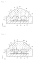
- FIG. 8 is a sectional view showing a light emitting device package according to a fourth modification of the first embodiment
- FIG. 9 is a sectional view showing a light emitting device package according to a fifth modification of the first embodiment.
- FIG.10 is a sectional view showing a light emitting device package according to a sixth modification of the first embodiment
- FIG.11 is a sectional view showing a light emitting device package according to a seventh modification of the first embodiment
- FIG.12 is a sectional view showing a light emitting device package according to an eighth modification of the first embodiment.
- FIG.13 is a sectional view showing a light emitting device package according to a ninth modification of the first embodiment
- FIG.14 is a sectional view showing a light emitting device package according to a tenth modification of the first embodiment
- FIG.15 is a sectional view showing a light emitting device package according to an eleventh modification of the first embodiment
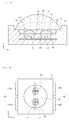
- FIG.16 is a plan view showing a light emitting device package according to an eleventh modification of the first embodiment
- FIGS. 17 and 18 are plan views showing other examples of the eleventh modification of the first embodiment
- FIG.19 is a sectional view showing a light emitting device package according to a twelfth modification of the first embodiment
- FIG.20 is a sectional view showing a light emitting device package according to a thirteenth modification of the first embodiment
- FIG. 21 is a sectional view showing a light emitting device package according to a second embodiment
- FIG. 22 is a sectional view showing a light emitting device package according to a third embodiment
- FIG. 23 is a sectional view showing a light emitting device package according to a first modification of the third embodiment
- FIG. 24 is a sectional view showing a light emitting device package according to a second modification of the third embodiment.
- FIG. 25 is a sectional view showing a light emitting device package according to a third modification of the third embodiment.
- FIG. 26 is a view showing a backlight unit including a light emitting device package according to the embodiment.
- FIG. 27 is a view showing a lighting system including a light emitting device package according to the embodiment.
- each layer shown in the drawings may be exaggerated, omitted or schematically drawn for the purpose of convenience or clarity.
- the size of elements does not utterly reflect an actual size.
- FIG. 1 is a perspective view showing a light emitting device package according to a first embodiment
- FIG. 2 is a perspective view showing a light emitting device package without an individual lens, a common lens, and a resin member.
- FIG. 3 is a plan view of FIG. 2 .
- a light emitting device package 100 may comprise a body 10 comprising a recess 20 and a plurality of light emitting device receiving part (hereinafter, referred to as "receiving part") 30, a plurality of light emitting devices 50 individually positioned in the receiving part 30, first and second electrodes 41 and 42, and a plurality of individual lenses 60.
- the light emitting device package 100 may comprise a common lens 70 to cover the individual lenses 60.
- the body 10 may comprise at least one of resin such as PPA (polyphthal amide), LCP (liquid crystal polymer), and PA9T (polyamid9T), metal, photo sensitive glass, sapphire (Al 2 O 3 ), a ceramic substrate, and printed circuit board (PCB), but the embodiment is not limited thereto.
- resin such as PPA (polyphthal amide), LCP (liquid crystal polymer), and PA9T (polyamid9T), metal, photo sensitive glass, sapphire (Al 2 O 3 ), a ceramic substrate, and printed circuit board (PCB), but the embodiment is not limited thereto.
- the body 10 may have various shapes according to the use and design of the light emitting device package 100.
- the body 10 may have various shapes such as a rectangular shape or a circular shape when viewed in a plan view.
- the body 10 has the recess 20 having an open upper portion.
- drawings show that the recess 20 has a circular shape when viewed in a plan view, the embodiment is not limited thereto. Accordingly, the recess 20 may have a polygonal shape comprising a rectangular shape when viewed in a plan view.
- a lateral surface of the recess 20 may be perpendicular to a bottom surface of the recess 20 or inclined with respect to the bottom surface of the recess 20. If the recess 20 has an inclined lateral surface, the lateral surface of the recess 20 may be inclined at an angle ( ⁇ 1 of FIG. 4 , and the same applies hereinafter) in a range of about 100° to about 170° to the bottom surface of the recess 20. If the angle ⁇ 1 is above 120°, a light emitted from the light emitting device 50 can be sufficiently reflected.
- a plurality of receiving parts 30 are formed in the bottom surface of the recess 20.
- the receiving parts 30 individually receive the light emitting devices 50.
- the receiving parts 30 When viewed in a plan view, the receiving parts 30 have a circular shape, but the embodiment is not limited thereto. Accordingly, the receiving parts 30 may have a polygonal shape comprising a rectangular shape when viewed in a plan view.
- a lateral surface of the receiving part 30 may be perpendicular to a bottom surface of the receiving part 30 or inclined with respect to the bottom surface of the receiving part 30. If the receiving part 30 has an inclined lateral surface, the lateral surface of the receiving part 30 may be inclined at an angle ( ⁇ 2 of FIG. 4 , and the same applies hereinafter) in a range of about 100° to about 170° to the bottom surface of the receiving part 30. If the angle ⁇ 2 is above 120°, a light emitted from the light emitting device 50 can be sufficiently reflected.
- the body 10 comprising the recess 20 and the receiving parts 30 may have a stack structure of multiple layers, or may be formed through an injection molding scheme. In addition, the body 10 may be formed through various schemes.
- the body 10 is provided therein with the first and second electrodes 41 and 42 electrically connected to the light emitting device 50.
- the first and second electrodes 41 and 42 may be formed by using a metallic plate having a predetermined thickness, and may be plated on the surface thereof with another metallic layer.
- the first and second electrodes 41 and 42 may comprise a metal having superior conductivity, and the metal may comprise a material selected from the group consisting of titanium (Ti), copper (Cu), nickel (Ni), gold (Au), chrome (Cr), tantalum (Ta), platinum (Pt), tin (Sn), and silver(Ag).
- first and second electrodes 41 and 42 may be exposed through the receiving parts 30, and remaining portions of the first and second electrodes 41 and 42 may be exposed to the outside through the inner part of the body 10.
- first and second electrodes 41 and 42 make contact with the bottom surface of the receiving part 30 according to the present embodiment, the embodiment is not limited thereto. Accordingly, the first and second electrodes 41 and 42 may make contact with the bottom surface of the recess 20, or may make contact with a top surface of the body 10.
- the light emitting device 50 is positioned in the receiving part 30 and electrically connected to the first and second electrodes 41 and 42.
- the light emitting device 50 may be electrically connected to the first and second electrodes 41 and 42 through a wire bonding scheme with a wire 52.
- the light emitting device 50 may be prepared in the form of a lateral-type chip in which two electrode layers are exposed upward, or a vertical-type chip in which two electrode layers are positioned in opposition to each other about a light emitting layer.
- the lateral-type chip may be coupled with the first and second electrodes 41 and 42 through the wire 52.
- the vertical-type chip may make contact with one of the first and second electrodes 41 and 42 and may be coupled with the other by the wire 52.
- FIGS. 2 and 3 show the lateral-type chip as an example.
- a die bonding scheme or a flip chip scheme may be employed to electrically connect the light emitting device 50 with the first and second electrodes 41 and 42.
- Resin members 82 and 84 are filled in the receiving part 30 to seal the light emitting device 50.
- the resin members 82 and 84 may comprise a transmissive material such as silicone or epoxy.
- the resin members 82 and 84 may comprise a luminescence material of absorbing a light emitted from the light emitting device 50 to emit a light having different wavelengths.
- Individual lenses 60 having a convex shape are positioned on the resin members 82 and 84.
- the individual lens 60 may be formed by molding resin, or may be provided by attaching a separately-manufactured lens.
- the resin members 82 and 84 have a structure different from that of the individual lenses 60 as shown in drawings or as described above, the resin members 82 and 84 may be formed together with the individual lenses 60 through the same process.
- the individual lenses 60 have at least portions making contact with the recess 20.
- the common lens 70 is provided on the recess 20 to cover the individual lenses 60.
- the common lens 70 may be formed by molding a resin or provided by attaching a separately-manufactured lens onto the recess 20. If the common lens 70 comprises a resin, the common lens 70 may comprise a fluorescence material. The common lens 70 may be separated from the individual lens 60.
- FIG. 4 is a sectional view taken along line IV-IV of FIG. 1 .
- one recess 20 is provided therein with a plurality of receiving parts 32 and 34 to individually receive a plurality of light emitting devices 50a and 50b.
- the receiving parts 32 and 34 may comprise the first and second receiving parts 32 and 34.
- the receiving parts 32 and 34 may have a depth H2 greater than those of light emitting devices 50a and 50b such that the resin members 82 and 84 may comprise a sufficient amount of luminescence material.
- the depth H2 of the receiving parts 32 and 34 may be above 30 ⁇ m greater than those of the light emitting devices 50a and 50b.
- the recess 20 has a depth H1 less than the depth H2 of the receiving parts 32 and 34. If the depth H1 of the recess 20 is excessively increased, an amount of lost light may be increased due to the reflection.
- the depth H1 of the recess 20 and the depth H2 of the receiving parts 32 and 34 are optimized, so that the efficiency of the light emitting device package 100 can be more improved.
- the light emitting devices 50a and 50b are provided in the receiving parts 32 and 34 as one-to-one correspondence.
- the first light emitting device 50a is provided in the first receiving part 32
- the second light emitting device 50b is provided in the second receiving part 34.
- the first resin member 82 is provided in the first receiving part 32
- the second resin member 84 is provided in the second receiving part 34.
- the first and second light emitting devices 50a and 50b may comprise homogenous light emitting devices to emit lights having the same wavelength or may comprise heterogeneous light emitting devices to emit lights having different wavelengths.
- the first resin member 82, the second resin member 84, and the common lens 70 may comprise homogeneous fluorescence material or heterogeneous fluorescence materials.
- the fluorescence material may comprise a material selected from the group consisting of sulfide, silicate, yttrium aluminum garnet (YAG), oxynitride, and nitride-based luminescence materials.
- the first and second light emitting devices 50a and 50b emit a blue light
- the first and second resin members 82 and 84 may comprise a fluorescence material to emit a yellow light (hereinafter, referred to as yellow fluorescence material).
- the first and second light emitting devices 50a and 50b emit a blue light
- the first resin member 82 may comprise a yellow fluorescence material
- the second resin member 84 may comprise a fluorescence material to emit a green light (hereinafter, referred to as a green fluorescence material).
- the combination of the first light emitting device 50a and the yellow fluorescence material can represent efficiency superior to efficiency represented in the combination of the second light emitting device 50b and the green fluorescence material.
- the common lens 70 may comprise a fluorescence material to emit a red light (hereinafter, referred to as red fluorescence material).
- the first and second resin members 82 and 84 may comprise different fluorescence materials. Therefore, fluorescence materials may be employed by taking the characteristic of the first and second light emitting devices 50a and 50b into consideration.
- heterogeneous fluorescence materials may be positioned in the receiving parts 32 and 34 and/or the recess 20, which are spaced different from each other, problems caused by the mixture of the heterogeneous fluorescence materials can be prevented.
- the red fluorescence material absorbs a light having a wavelength changed by another fluorescence material. Accordingly, the whole brightness and efficiency can be degraded.
- the red fluorescence material is positioned at a space different from that of another fluorescence material, so that brightness can be prevented from being degraded.
- a first individual lens 60a is provided on the first receiving part 32, and a second individual lens 60b spaced apart from the first individual lens 60a is positioned on the second receiving part 34.
- the first and second individual lenses 60a and 60b may be provided on the lateral surface of the recess 20 while being spaced apart from each other at a predetermined distance, and may have a convex shape on the light emitting devices 50a and 50b, respectively.
- the lens may have a smooth-curved surface. Accordingly, the total refection excessively occurs on the surface of the lens, so that the light efficiency can be reduced.
- the lens surface may have a greater curvature. Accordingly, the total reflection can be reduced, so that the light efficiency can be improved.
- the first and second individual lenses 60a and 60b may have a substantially-hemispherical shape when taking light efficiency into consideration.
- the hemispherical lens is used when one lens is used for the light emitting devices 50a and 50b, the thickness of the light emitting device package 100 may be excessively thickened. Accordingly, the hemispherical lens cannot be used.
- the first and second individual lenses 60a and 60b since the first and second individual lenses 60a and 60b are separately employed, the first and second individual lenses 60a and 60b may have a hemispherical shape representing superior light efficiency.
- the shapes and the materials of the first and second individual lenses 60a and 60b may be determined while taking the characteristics of the first and second light emitting devices 50a and 50b into consideration. Therefore, the light emitting device package 100 may be formed in various structures. Another embodiment of employing different shapes and different materials in the first and second individual lenses 60a and 60b will be described with reference to FIGS. 22 to 25 below.
- the common lens 70 is provided to cover the first and second individual lenses 60a and 60b. Since the common lens 70 has a refractive index smaller than those of the first and second individual lenses 60a and 60b, light extraction efficiency can be more improved. In other words, since a light is transmitted from a material having a high refractive index to a material having a low refractive index, light loss caused by Fresnel reflection can be minimized.
- various light emitting device packages 100 can be manufactured by taking the characteristics of the light emitting devices 50a and 50b into consideration. Accordingly, the efficiency of the light emitting device package 100 can be improved.
- FIG. 5 is a sectional view showing a light emitting device package according to a first modification of the first embodiment.
- a concave part 602 is formed at an upper portion of an individual lens 602.
- the concave part 602a may be recessed toward the bottom surface of the recess 20, and connected with the individual lens 602 while forming a gently-curved surface.
- the concave part 602a guides a light so that the light can be extracted to the outside through a peripheral portion of the individual lens 602. In other words, the orientation angle of the light can be widened by using the individual lens 602.
- FIG. 6 is a sectional view showing a light emitting device package according to a second modification of the first embodiment.
- the concave part 602a is formed at the upper portion of an individual lens 602 in the light emitting device package according to the present modification, and a reflective material 604 is provided in the concave part 602a.
- the reflective material 604 may occupy about 5% to about 60% of the top surface of the individual lens 602.
- the reflective material 604 provided in the concave part 602a reflects a light emitted from the light emitting device 50 or a light traveling to the concave part 602a among lights reflected by the lateral surface or the bottom surface of the receiving part 30. Therefore, the light emitted from the light emitting device 50 or the light reflected by the lateral surface or the bottom surface of the receiving part 30 is extracted to the outside through a region without the concave part 602a. Accordingly, since a light is extracted to the outside through the peripheral portion of the individual lens 602, a light having a wide orientation angle can be provided.
- the reflective material 604 may be formed by mixing an organic material having above 70% of transmittance with an inorganic material capable of reflecting or scattering a light and provided in the concave part 602a.
- the inorganic material may comprise at least one selected from the group consisting of TiO 2 , SiO 2 , Al, Al 2 O 3 , and Ag.
- a light can be totally reflected or partially reflected according to mixture ratios of the organic material and the inorganic material.
- the mixture ratio of the organic material and the inorganic material may be in the range of 1:0.001 to 1:1.
- the reflective material 604 may comprise a deposition layer comprising at least one selected from the group consisting of SiO 2 , TiO 2 , Al, Ag, and Ti.
- the deposition layer may have a thickness of about 100 .
- the concave part 602a is formed in the individual lens 602 overlapping with the light emitting device 50 perpendicularly to the light emitting device 50, and the reflective material 604 is provided in the concave part 602a, so that the orientation angle of the light emitted from the light emitting device 50 can be adjusted.
- FIG. 7 is a sectional view showing a light emitting device package according to a third modification of the first embodiment.
- an individual lens 606 is provided on a surface thereof with a predetermined pattern, for example, a concavoconvex pattern.
- This pattern refracts or diffuses a light emitted from the light emitting device 50 when the light is transmitted or reflected. Accordingly, a light may be emitted with uniform light intensity distribution from the central portion or the lateral portion of the individual lens 606. In addition, color variation between the central portion and the lateral portion of the individual lens 606 can be reduced.
- FIG. 8 is a sectional view showing a light emitting device package according to a fourth modification of the first embodiment.
- an individual lens 608 may comprise a rectangular lens in the light emitting device package according to the present modification. As described above, according to the present modification, the individual lens 608 may have various shapes.
- FIG. 9 is a sectional view showing a light emitting device package according to a fifth modification of the first embodiment.
- an individual lens 610 may comprise a rectangular lens, and the individual lens 610 may comprise a micro-lens 610a.
- FIG. 9 shows that the micro-lens 610a has a triangular sectional surface as an example, the present modification is not limited thereto. Accordingly, the micro-lens 610a may have a circular sectional surface, an oval sectional surface, or a polygonal sectional surface.
- the individual lens 610 having the micro-lens 610a can easily mix colors of lights with each other by refracting lights emitted from the light emitting device 50.
- FIG. 10 is a sectional view showing a light emitting device package according to a sixth modification of the first embodiment.
- an individual lens 612 may comprise a rectangular lens, and a concave part 612a is formed at the upper portion of the individual lens 612.
- the orientation angle of the light emitted from the light emitting device 50 can be widened by the concave part 612a.
- FIG. 11 is a sectional view showing a light emitting device package according to a seventh modification of the first embodiment.
- the common lens 72 may comprise a rectangular lens. As described above, according to the present modification, the common lens 72 having various shapes may be used. The common lens 72 may be provided therein with the micro-lens shown in FIG. 9 or the concave part shown in FIG. 10 .
- FIGS. 12 to 14 A modification in the arrangement of a fluorescence material according to the first embodiment will be described with reference to FIGS. 12 to 14 .
- structures and components same to or greatly similar to those of the first embodiment will not be further described, and only structures and components different from those of the first embodiment will be described in detail.
- FIG. 12 is a sectional view showing a light emitting device package according to an eighth modification of the first embodiment.
- the present modification makes a difference from the first embodiment of employing resin comprising a fluorescence material and filled in the receiving part 30 in that a film 802 comprising a fluorescence material is coated on the light emitting device 50.
- the film 802 may be formed by inserting a fluorescence material into a transmissive film.
- the transmissive film may comprise a transparent material comprising one selected from the group consisting of polycarbonate, poly (methyl methacrylate), polypropylene, quartz, and glass.
- the fluorescence material may comprise a material selected from the group consisting of sulfide, silicate, yttrium aluminum garnet (YAG), oxynitride, and nitride-based fluorescence materials.
- the fluorescence material can be uniformly distributed on the light emitting device 50 contributing to light emission.
- FIG. 13 is a sectional view showing a light emitting device package according to a ninth modification of the first embodiment.
- the film 802 comprising a fluorescence material is coated on the light emitting device 50, and a resin member 804 may be filled in other inner parts of the receiving part 30.
- the resin member 804 may comprise epoxy or silicone.
- the film 802 may be more stably provided on the light emitting device 50 by the resin member 804.
- FIG. 14 is a sectional view showing a light emitting device package according to a tenth modification according to the first embodiment.
- a step 302a is formed at an upper portion of the receiving part 302, and the film 802 comprising a fluorescence material is provided in the step 302a.
- the step 302a is formed at the upper portion of the receiving part 302, so that the film 802 can be stably fixed on the step 302a.
- the step 302a may have a depth substantially same to the thickness of the film 802. However, the embodiment is not limited thereto, and the depth of the step 302a may be thinner than or thicker than the thickness of the film 802.
- FIG. 14 shows the receiving part 302 having an empty space below the film 802, a resin member may be formed in the empty space as shown in FIG. 13 .
- FIGS. 15 to 19 A modification of the body according to the first embodiment will be described with reference to FIGS. 15 to 19 .
- structures and components same to or greatly similar to those of the first embodiment will not be further described, and only structures and components different from those of the first embodiment will be described in detail.
- FIG. 15 is a sectional view showing a light emitting device package according to an eleventh modification of the first embodiment
- FIG. 16 is a plan view showing the light emitting device package according to the eleventh modification of the first embodiment
- FIGS. 17 and 18 are plan views showing other examples of the eleventh modification of the first embodiment according to the present invention.
- the body 10 may comprise a guide member 102 to guide and fix the individual lens 60.
- the guide member 102 may be manufactured through a separate process and attached to the body 10.
- the guide member 102 may be formed integrally with the body 10 through an injection molding process of forming the body 10.
- the guide member 102 may have a closed loop shape formed along the edge of the individual lens 60. According to the present modification, since the individual lens 60 has a circular shape when viewed in a plan view, the guide member 102 may have a circular shape. If the individual lens 60 has a rectangular shape when viewed in a plan view, the guide member 102 may have a rectangular shape having a portion punched corresponding to the individual lens 60.
- the individual lens 60 may be formed on a position on the light emitting device 50 capable of maximizing light efficiency
- FIG. 16 shows that the guide member 102 is integrated in one form to guide a plurality of individual lenses 60
- the present embodiment is not limited thereto.
- guide members 104 are spaced apart from each other to guide the individual lenses 60, respectively.
- the guide member 106 may have a straight line shape between the lenses 60.
- the guide member 105 may have various plan shapes.
- FIG. 19 is a sectional view showing a light emitting device package according to a twelfth modification of the first embodiment.
- a body 10a according to the present modification may comprise a step 108 to fix the common lens 74 on the upper portion of the body 10a.
- the common lens 74 is a separately-manufactured lens, and a resin member 88 is filled in the recess 20 below the common lens 74.
- the resin member 88 may comprise a fluorescence material.
- the common lens 74 can be firmly fixed on a desired position by the step 108.
- FIG. 20 is a sectional view showing a light emitting device package according to a thirteenth modification of the first embodiment.
- the first electrode 41 may comprise a plurality of electrode parts 41a and 41b corresponding to a plurality of light emitting devices 50
- the second electrode 42 may comprise a plurality of light emitting parts 42a and 42b corresponding to the light emitting devices 50. Accordingly, the light emitting devices 50 can be individually driven.
- FIG. 21 is a sectional view showing a light emitting device package according to the second embodiment.
- three receiving parts 32, 34, and 36, three light emitting devices 50a, 50b, and 50c, and three individual lenses 60a, 60b, and 60c are positioned in one recess 20.
- FIG. 21 shows that the receiving parts 32, 34, and 36 are arranged in one row, the embodiment is not limited thereto. Accordingly, at least four receiving parts may be formed and arranged in a polygonal structure, or arranged in at least two rows.
- the first to third light emitting devices 50a, 50b, and 50c may comprise homogeneous light emitting devices to emit lights having the same wavelengths, or heterogeneous light emitting devices to emit lights having different wavelengths.
- the first and second resin members 82 and 84 and/or the third resin member 86 may comprise homogeneous fluorescence materials or heterogeneous fluorescence materials.
- the first to third light emitting devices 50a, 50b, and 50c may emit a blue light
- the first to third resin members 82, 84, and 86 may comprise a yellow fluorescence material.
- the first to third light emitting devices 50a, 50b, and 50c emit a blue light
- the first to third resin members 82, 84, and 86 may comprise blue and red luminescence materials.
- the first to third light emitting devices 50a, 50b, and 50c emit a blue light
- the first to third resin members 82, 84, and 86 may comprise green, red, yellow fluorescence materials.
- the first to third light emitting devices 50a, 50b, and 50c emit a blue light
- the first to third resin members 82, 84, and 86 may comprise yellow, green, and red fluorescence materials.
- the highest light efficiency can be represented in the combination of the first light emitting device 50a and the yellow fluorescence material
- the lowest light efficiency can be represented in the combination of the third light emitting device 50c and the red fluorescence material.
- the first to third light emitting devices 50a, 50b, and 50c emit a green light, a blue light, and a red light, respectively.
- the first and third resin members 82 and 86 may not comprise a fluorescence material
- the second resin member 84 may comprise a yellow fluorescence material.
- the highest light efficiency is represented in the first light emitting device 50a
- the second highest light efficiency is represented in the combination of the second light emitting device 50b and the yellow fluorescence material
- the lowest light efficiency is represented in the third light emitting device 50c.
- the first to third light emitting devices 50a, 50b, and 50c emit a UV light.
- the first to third resin members 82, 84, and 86 may comprise fluorescence materials to emit yellow, green, and red lights, respectively.
- the highest light efficiency is represented in the combination of the first light emitting device 50a and the yellow fluorescence material
- the lowest light efficiency is represented in the third light emitting device 50c and the red fluorescence material.
- the light emitting devices and the fluorescence materials may have various combination forms.
- FIG. 22 is a sectional view showing the light emitting device package according to the third embodiment
- FIG. 23 is a sectional view showing a light emitting device package according to a first modification of the third embodiment.
- a first individual lens 614a and a second individual lens 614b have different shapes.
- first and second individual lenses 614a and 614b may have different diameters and heights, so that curvatures of the first and second individual lenses 614a and 614b are different from each other.
- This structure is designed by taking into consideration a fact that the efficiency of the first light emitting device 50a is different from the efficiency of the second light emitting device 50b.
- the efficiency of the first light emitting device 50a refers to the efficiency represented by the combination of the first light emitting device 50a and the fluorescence material if the first resin member 32 comprises a fluorescence material, or refers to the efficiency represented by the first light emitting device 50a if the first resin member 32 does not comprise a fluorescence material.
- the efficiency of the second light emitting device 50b refers to the efficiency represented by the combination of the second light emitting device 50b and a fluorescence material if the second resin member 34 comprise the fluorescence material, or refers to the efficiency represented by the first light emitting device 50b if the second resin member 34 does not comprise a fluorescence material.
- the efficiency of the first light emitting device 50a is greater than the efficiency of the second light emitting device 50b.
- the shape of the second individual lens 614b corresponding to the second light emitting device 50b is more similar to a hemispherical shape than the shape of the first individual lens 614a corresponding to the first light emitting device 50a is similar to the hemispherical shape.
- the second individual lens 614b has a shape more similar to a hemispherical shape, the second individual lens 614b represents light efficiency superior to that of the first individual lens 614a. Accordingly, the lower efficiency of the second light emitting device 50b can be enhanced. Therefore, the efficiency difference between the first and second light emitting devices 50a and 50b can be uniformed.
- the ratio of a diameter W2 to a height T2 may be 2:1.
- a diameter W1 of the first individual lens 614a is same to the diameter W2 of the second individual lens 614b, and a height T1 of the first individual lens 614a may be lower than the height T2 of the second individual lens 614b. Therefore, the ratio of the diameter W1 to the height T1 of the first individual lens 614a may be greater than 2:1.
- the ratio of the diameter W2 to the height T2 of the second individual lens 614b more approximates 2:1 than the ratio of the diameter W1 to the height T1 of the first individual lens 614a approximates.
- FIG. 22 shows that the height T1 of the first individual lens 614a is less than the height T2 of the second individual lens 614b
- the present embodiment is not limited thereto. Therefore, as shown in FIG. 23 , a height T3 of the first individual lens 614c may be greater than the height t2 of the second individual lens 614b. Therefore, the ratio of the width W1 to the height T3 of the first individual lens 614c becomes less than 2:1. Therefore, the diameter W2 to the height T2 of the second individual lens 614b more approximates 2:1 than the ratio of the diameter W1 to the height T3 of the first individual lens 614c approximates.
- individual lenses having light extraction efficiencies different from each other can be provided by changing the widths of the individual lenses.
- the individual lenses 614a and 614b are formed with respect to the light emitting devices 50a and 50b, respectively, the individual lenses 614a and 614b may have various shapes. Therefore, different characteristics of the light emitting devices 50a and 50b are compensated, so that a light can be uniformly extracted.
- FIG. 24 is a sectional view showing a light emitting device package according to a second modification of the third embodiment.
- a first individual lens 616a corresponding to the first light emitting device 50a may comprise a material different from a material constituting the second individual lens 616b corresponding to the second light emitting device 50b.
- the efficiency of the first light emitting device 50a may be higher than the efficiency of the second light emitting device 50b.
- a first individual lens 616a may comprise a material having a refractive index in the range of about 1.4 to about 1.5
- a second individual lens 616b may comprise a material having a refractive index in the range of about 1.5 to about 1.6.
- the first and second individual lenses 616a and 616b may comprise various materials.
- a lens comprises a material having a refractive index of about 1.5 rather than a material having a refractive index of about 1.4
- light efficiency can be more increased. Therefore, the light efficiency of the second individual lens 616b comprising a material having a refractive index of about 1.5 is higher than the light efficiency of the first individual lens 616a. Therefore, the difference in the efficiency between the first and second light emitting devices 50a and 50b can be compensated.
- a lens having higher light extraction efficiency is formed on the second light emitting device 50b having lower efficiency, and a lens having lower light extraction efficiency is formed on the first light emitting device 50a having higher light extraction efficiency.
- FIG. 25 is a sectional view showing a light emitting device package according to a third modification of a third embodiment.
- a first individual lens 618a may comprise a convex lens
- a second individual lens 618b may have an upper portion provided therein with a concave part 618 filled with a reflective material 620.
- the individual lenses 618a and 618b having different structures are used together.
- the present modification is not limited to the case shown in FIG. 25 . Accordingly, the individual lenses 618a and 618b may comprise individual lenses shown in FIGS. 4 to 10 .
- the light emitting device package according to the embodiments and the modifications may serve as a lighting system such as a backlight unit, an indicator, a lamp or a streetlamp, and the details thereof will be described with reference to FIGS. 26 and 27 .
- FIG. 26 is a perspective view showing a backlight unit 1100 comprising the light emitting device package according to the embodiment.
- the backlight unit 1100 shown in FIG. 26 is one example of the lighting system, and the embodiment is not limited thereto.
- the backlight unit 1100 may comprise a bottom cover 1140, a light guide member 1120 provided in the bottom cover 1140, and a light emitting module 1110 provided at one side or on the bottom surface of the light guide member 1120.
- a reflective sheet 1130 is disposed below the light guide member 1120.
- the bottom cover 1140 has a box shape having an open top surface to receive the light guide member 1120, the light emitting module 1110 and the reflective sheet 1130 therein.
- the bottom cover 1140 may comprise metallic material or resin material, but the embodiment is not limited thereto.
- the light emitting module 1110 may comprise a plurality of light emitting devices 600 provided on a substrate 700.
- the light emitting devices 600 provide the light to the light guide member 1120.
- the light emitting module 1110 is provided on at least one inner side of the bottom cover 1140 to provide the light to at least one side of the light guide member 1120.
- the light emitting module 1110 may be provided under the light guide member 1120 in the bottom cover 1140 to provide the light toward the bottom surface of the light guide member 1120. Such an arrangement can be variously changed according to the design of the backlight unit 1100.
- the light guide member 1120 may be provided in the bottom cover 1140.
- the light guide member 1120 converts the light emitted from the light emitting module 1110 into the surface light to guide the surface light toward a display panel (not shown).
- the light guide member 1120 may comprise a light guide plate.
- the light guide plate can be manufactured by using acryl-based resin, such as PMMA (polymethyl methacrylate), PET (polyethylene terephthalate), COC, PC (polycarbonate) or PEN (polyethylene naphthalate) resin.
- PMMA polymethyl methacrylate
- PET polyethylene terephthalate
- COC polyethylene terephthalate
- PC polycarbonate
- PEN polyethylene naphthalate
- An optical sheet 1150 may be provided above the light guide member 1120.
- the optical sheet 1150 may comprise at least one of a diffusion sheet, a light collection sheet, a brightness enhancement sheet, and a fluorescent sheet.
- the optical sheet 1150 has a stack structure of the diffusion sheet, the light collection sheet, the brightness enhancement sheet, and the fluorescent sheet.
- the diffusion sheet uniformly diffuses the light emitted from the light emitting module 1110 such that the diffused light can be concentrated onto the display panel (not shown) by the light collection sheet.
- the light output from the light collection sheet is randomly polarized and the brightness enhancement sheet increases the degree of polarization of the light output from the light collection sheet.
- the light collection sheet may comprise a horizontal and/or vertical prism sheet.
- the brightness enhancement sheet may comprise a dual brightness enhancement film and the fluorescent sheet may comprise a transmittive plate or a transmittive film comprising fluorescence materials.
- the reflective sheet 1130 may be disposed below the light guide member 1120.
- the reflective sheet 1130 reflects the light, which is emitted through the bottom surface of the light guide member 1120, toward the light exit surface of the light guide member 1120.
- the reflective sheet 1130 may comprise resin material having a high reflectance, such as PET, PC or PVC resin, but the embodiment is not limited thereto.
- FIG. 27 is a perspective view showing a lighting system 1200 comprising the light emitting device package according to the embodiment.
- the lighting system 1200 shown in FIG. 27 is only one example and the embodiment is not limited thereto.
- the lighting system 1200 may comprise a case body 1210, a light emitting module 1230 provided in the case body 1210, and a connection terminal 1220 provided in the case body 1210 to receive power from an external power source.
- the case body 1210 may comprise material having superior heat dissipation property.
- the case body 1210 may comprise metallic material or resin material.
- the light emitting module 1230 may comprise a board 700 and at least one light emitting device 600 provided on the board 700.
- the board 700 may comprise an insulating member printed with a circuit pattern.
- the board 700 comprises a PCB (printed circuit board), an MC (metal core) PCB, a flexible PCB, or a ceramic PCB.
- the board 700 may comprise material that effectively reflects the light.
- the surface of the board 700 can be coated with a color, such as a white color or a silver color, to effectively reflect the light.
- At least one light emitting device 600 can be provided on the board 700.
- Each light emitting device 600 may comprise at least one LED (light emitting diode).
- the LED may comprise a colored LED that emits the light having the color of red, green, blue or white and a UV (ultraviolet) LED that emits UV light.
- the light emitting module 1230 has various combinations of light emitting devices to provide various colors and brightness.
- the white LED, the red LED and the green LED can be combined to achieve the high color rendering index (CRI).
- a fluorescent sheet may be provided in the path of the light emitted from the light emitting module 1230 to change the wavelength of the light emitted from the light emitting module 1230.
- the fluorescent sheet may comprise yellow fluorescence material. In this case, the light emitted from the light emitting module 1230 passes through the fluorescent sheet so that the light is viewed as white light.
- connection terminal 1220 is electrically connected to the light emitting module 1230 to supply power to the light emitting module 1230.
- the connection terminal 1220 has a shape of a socket screw-coupled with the external power source, but the embodiment is not limited thereto.
- the connection terminal 1220 may be prepared in the form of a pin inserted into the external power source or connected to the external power source through a wire.
- At least one of the light guide member, the diffusion sheet, the light collection sheet, the brightness enhancement sheet and the fluorescent sheet is provided in the path of the light emitted from the light emitting module, so that the desired optical effect can be achieved.
- the lighting system comprises a light emitting device package capable of improving light efficiency and emitting uniform light, so that superior light efficiency and characteristic can be realized.
- any reference in this specification to "one embodiment,” “an embodiment,” “example embodiment,” etc. means that a particular feature, structure, or characteristic described in connection with the embodiment is included in at least one embodiment of the invention.
- the appearances of such phrases in various places in the specification are not necessarily all referring to the same embodiment.
Landscapes
- Led Device Packages (AREA)
- Non-Portable Lighting Devices Or Systems Thereof (AREA)
Abstract
Description
- The embodiment relates to a light emitting device package and a lighting system.
- Light emitting diodes (LEDs) are a kind of semiconductor devices that convert electric energy into light. The LED is advantageous as compared with conventional light sources, such as a fluorescent lamp or a glow lamp, in terms of power consumption, life span, response speed, safety and environmental-friendly requirement.
- In this regard, various studies have been performed to replace the conventional light sources with the LEDs. The LEDs are increasingly used as light sources for lighting devices such as various lamps, liquid crystal displays, electric signboards, and street lamps.
- The embodiment provides a light emitting device package capable of improving light efficiency and a lighting system having the light emitting device package.
- The embodiment provides a light emitting device package capable of uniformly discharging light and a lighting system having the light emitting device package.
- According to the embodiment, a light emitting device package comprises a body comprising a recess and a plurality of light emitting device receiving parts formed in a bottom surface of the recess, a plurality of light emitting devices separately positioned in the light emitting device receiving parts, a plurality of individual lenses spaced apart from each other on the light emitting device receiving parts, and a common lens covering the individual lenses.
- According to the embodiment, a lighting system comprises a board, and a light emitting module comprising a light emitting device package provided on the board. The light emitting device comprises a body comprising a recess and a plurality of light emitting device receiving parts formed in a bottom surface of the recess, a plurality of light emitting devices separately positioned in the light emitting device receiving parts, a plurality of individual lenses spaced apart from each other on the light emitting device receiving parts, and a common lens covering the individual lenses.
- As described above, according to the present embodiment, the receiving parts, the resin members, and individual lenses are provided corresponding to each of light emitting devices. Therefore, since the individual lenses can have a structure suitable for light efficiency, the efficiency of the light emitting device package can be improved.
- In addition to the individual lenses, the common lens having a refractive index lower than that of the individual lenses is additionally provided, so that efficiency can be more improved.
- In addition, based on the characteristics of the light emitting devices, the resin members may comprise different luminescence materials, or the individual lenses may have different shapes and different characteristics. Therefore, various light emitting device packages can be manufactured suitably for desired characteristics. In particular, if the individual lenses have different curvatures or different refractive indexes based on the efficiency, a light can be uniformly discharged even in various types of the combination of light emitting devices and luminescence materials.
-
FIG. 1 is a perspective view showing a light emitting device package according to a first embodiment; -
FIG. 2 is a perspective view showing a light emitting device package ofFIG. 1 without individual lenses, common lenses, and resin members; -
FIG. 3 is a plan view ofFIG. 2 ; -
FIG. 4 is a sectional view taken along line IV-IV ofFIG. 1 ; -
FIG. 5 is a sectional view showing a light emitting device package according to a first modification of a first embodiment; -
FIG. 6 is a sectional view showing a light emitting device package according to a second modification of the first embodiment; -
FIG. 7 is a sectional view showing a light emitting device package according to a third modification of the first embodiment; -
FIG. 8 is a sectional view showing a light emitting device package according to a fourth modification of the first embodiment; -
FIG. 9 is a sectional view showing a light emitting device package according to a fifth modification of the first embodiment; -
FIG.10 is a sectional view showing a light emitting device package according to a sixth modification of the first embodiment; -
FIG.11 is a sectional view showing a light emitting device package according to a seventh modification of the first embodiment; -
FIG.12 is a sectional view showing a light emitting device package according to an eighth modification of the first embodiment; -
FIG.13 is a sectional view showing a light emitting device package according to a ninth modification of the first embodiment; -
FIG.14 is a sectional view showing a light emitting device package according to a tenth modification of the first embodiment; -
FIG.15 is a sectional view showing a light emitting device package according to an eleventh modification of the first embodiment; -
FIG.16 is a plan view showing a light emitting device package according to an eleventh modification of the first embodiment; -
FIGS. 17 and 18 are plan views showing other examples of the eleventh modification of the first embodiment; -
FIG.19 is a sectional view showing a light emitting device package according to a twelfth modification of the first embodiment; -
FIG.20 is a sectional view showing a light emitting device package according to a thirteenth modification of the first embodiment; -
FIG. 21 is a sectional view showing a light emitting device package according to a second embodiment; -
FIG. 22 is a sectional view showing a light emitting device package according to a third embodiment; -
FIG. 23 is a sectional view showing a light emitting device package according to a first modification of the third embodiment; -
FIG. 24 is a sectional view showing a light emitting device package according to a second modification of the third embodiment; -
FIG. 25 is a sectional view showing a light emitting device package according to a third modification of the third embodiment; -
FIG. 26 is a view showing a backlight unit including a light emitting device package according to the embodiment; and -
FIG. 27 is a view showing a lighting system including a light emitting device package according to the embodiment. - In the description of the embodiments, it will be understood that, when a layer (or film), a region, a pattern, or a structure is referred to as being "on" or "under" another substrate, another layer (or film), another region, another pad, or another pattern, it can be "directly" or "indirectly" over the other substrate, layer (or film), region, pad, or pattern, or one or more intervening layers may also be present. Such a position of the layer has been described with reference to the drawings.
- The thickness and size of each layer shown in the drawings may be exaggerated, omitted or schematically drawn for the purpose of convenience or clarity. In addition, the size of elements does not utterly reflect an actual size.
- Hereinafter, embodiments will be described with reference to accompanying drawings.
-
FIG. 1 is a perspective view showing a light emitting device package according to a first embodiment, andFIG. 2 is a perspective view showing a light emitting device package without an individual lens, a common lens, and a resin member.FIG. 3 is a plan view ofFIG. 2 . - Referring to
FIG. 1 to 3 , a lightemitting device package 100 according to the first embodiment may comprise abody 10 comprising arecess 20 and a plurality of light emitting device receiving part (hereinafter, referred to as "receiving part") 30, a plurality oflight emitting devices 50 individually positioned in thereceiving part 30, first andsecond electrodes individual lenses 60. In addition, the lightemitting device package 100 may comprise acommon lens 70 to cover theindividual lenses 60. - Hereinafter, the above structure will be described in more detail.
- The
body 10 may comprise at least one of resin such as PPA (polyphthal amide), LCP (liquid crystal polymer), and PA9T (polyamid9T), metal, photo sensitive glass, sapphire (Al2O3), a ceramic substrate, and printed circuit board (PCB), but the embodiment is not limited thereto. - The
body 10 may have various shapes according to the use and design of the lightemitting device package 100. For instance, thebody 10 may have various shapes such as a rectangular shape or a circular shape when viewed in a plan view. - The
body 10 has therecess 20 having an open upper portion. Although drawings show that therecess 20 has a circular shape when viewed in a plan view, the embodiment is not limited thereto. Accordingly, therecess 20 may have a polygonal shape comprising a rectangular shape when viewed in a plan view. - A lateral surface of the
recess 20 may be perpendicular to a bottom surface of therecess 20 or inclined with respect to the bottom surface of therecess 20. If therecess 20 has an inclined lateral surface, the lateral surface of therecess 20 may be inclined at an angle (θ1 ofFIG. 4 , and the same applies hereinafter) in a range of about 100° to about 170° to the bottom surface of therecess 20. If the angle θ1 is above 120°, a light emitted from thelight emitting device 50 can be sufficiently reflected. - A plurality of receiving
parts 30 are formed in the bottom surface of therecess 20. The receivingparts 30 individually receive thelight emitting devices 50. When viewed in a plan view, the receivingparts 30 have a circular shape, but the embodiment is not limited thereto. Accordingly, the receivingparts 30 may have a polygonal shape comprising a rectangular shape when viewed in a plan view. - A lateral surface of the receiving
part 30 may be perpendicular to a bottom surface of the receivingpart 30 or inclined with respect to the bottom surface of the receivingpart 30. If the receivingpart 30 has an inclined lateral surface, the lateral surface of the receivingpart 30 may be inclined at an angle (θ2 ofFIG. 4 , and the same applies hereinafter) in a range of about 100° to about 170° to the bottom surface of the receivingpart 30. If the angle θ2 is above 120°, a light emitted from thelight emitting device 50 can be sufficiently reflected. - The
body 10 comprising therecess 20 and the receivingparts 30 may have a stack structure of multiple layers, or may be formed through an injection molding scheme. In addition, thebody 10 may be formed through various schemes. - The
body 10 is provided therein with the first andsecond electrodes light emitting device 50. The first andsecond electrodes second electrodes - Portions of the first and
second electrodes parts 30, and remaining portions of the first andsecond electrodes body 10. Although the first andsecond electrodes part 30 according to the present embodiment, the embodiment is not limited thereto. Accordingly, the first andsecond electrodes recess 20, or may make contact with a top surface of thebody 10. - The
light emitting device 50 is positioned in the receivingpart 30 and electrically connected to the first andsecond electrodes light emitting device 50 may be electrically connected to the first andsecond electrodes wire 52. - The
light emitting device 50 may be prepared in the form of a lateral-type chip in which two electrode layers are exposed upward, or a vertical-type chip in which two electrode layers are positioned in opposition to each other about a light emitting layer. In this case, the lateral-type chip may be coupled with the first andsecond electrodes wire 52. The vertical-type chip may make contact with one of the first andsecond electrodes wire 52.FIGS. 2 and3 show the lateral-type chip as an example. - However, the embodiment is not limited thereto. In other words, in addition to the wire bonding scheme, a die bonding scheme or a flip chip scheme may be employed to electrically connect the
light emitting device 50 with the first andsecond electrodes -
Resin members 82 and 84 (seeFIG. 4 , and the same applies hereinafter) are filled in the receivingpart 30 to seal thelight emitting device 50. Theresin members resin members light emitting device 50 to emit a light having different wavelengths. -
Individual lenses 60 having a convex shape are positioned on theresin members individual lens 60 may be formed by molding resin, or may be provided by attaching a separately-manufactured lens. Although theresin members individual lenses 60 as shown in drawings or as described above, theresin members individual lenses 60 through the same process. Theindividual lenses 60 have at least portions making contact with therecess 20. - The
common lens 70 is provided on therecess 20 to cover theindividual lenses 60. Thecommon lens 70 may be formed by molding a resin or provided by attaching a separately-manufactured lens onto therecess 20. If thecommon lens 70 comprises a resin, thecommon lens 70 may comprise a fluorescence material. Thecommon lens 70 may be separated from theindividual lens 60. - Hereinafter, the
recess 20, the receivingpart 30, thelight emitting device 50, theindividual lens 60, thecommon lens 70, and theresin members FIG. 4. FIG. 4 is a sectional view taken along line IV-IV ofFIG. 1 . - According to the present embodiment, one
recess 20 is provided therein with a plurality of receivingparts devices parts parts - In this case, if the
resin members parts devices resin members parts light emitting devices recess 20 has a depth H1 less than the depth H2 of the receivingparts recess 20 is excessively increased, an amount of lost light may be increased due to the reflection. - As described above, according to the present embodiment, the depth H1 of the
recess 20 and the depth H2 of the receivingparts device package 100 can be more improved. - The
light emitting devices parts light emitting device 50a is provided in the first receivingpart 32, and the secondlight emitting device 50b is provided in the second receivingpart 34. In addition, thefirst resin member 82 is provided in the first receivingpart 32, and thesecond resin member 84 is provided in the second receivingpart 34. - In this case, the first and second
light emitting devices first resin member 82, thesecond resin member 84, and thecommon lens 70 may comprise homogeneous fluorescence material or heterogeneous fluorescence materials. The fluorescence material may comprise a material selected from the group consisting of sulfide, silicate, yttrium aluminum garnet (YAG), oxynitride, and nitride-based luminescence materials. - According to one example, the first and second
light emitting devices second resin members - According to anther embodiment, the first and second
light emitting devices first resin member 82 may comprise a yellow fluorescence material, and thesecond resin member 84 may comprise a fluorescence material to emit a green light (hereinafter, referred to as a green fluorescence material). In this case, the combination of the firstlight emitting device 50a and the yellow fluorescence material can represent efficiency superior to efficiency represented in the combination of the secondlight emitting device 50b and the green fluorescence material. In addition, thecommon lens 70 may comprise a fluorescence material to emit a red light (hereinafter, referred to as red fluorescence material). - In other words, since only one resin member can be used according to the related art, different resin members cannot be used for the
light emitting devices light emitting devices parts second resin members light emitting devices - In addition, since heterogeneous fluorescence materials may be positioned in the receiving
parts recess 20, which are spaced different from each other, problems caused by the mixture of the heterogeneous fluorescence materials can be prevented. For example, when a red fluorescence material is mixed with another fluorescence material, the red fluorescence material absorbs a light having a wavelength changed by another fluorescence material. Accordingly, the whole brightness and efficiency can be degraded. According to the present invention, the red fluorescence material is positioned at a space different from that of another fluorescence material, so that brightness can be prevented from being degraded. - A first
individual lens 60a is provided on the first receivingpart 32, and a secondindividual lens 60b spaced apart from the firstindividual lens 60a is positioned on the second receivingpart 34. According to the present embodiment, the first and secondindividual lenses recess 20 while being spaced apart from each other at a predetermined distance, and may have a convex shape on thelight emitting devices - If only one lens is provided corresponding to the
light emitting devices individual lenses light emitting devices - In this case, the first and second
individual lenses light emitting devices device package 100 may be excessively thickened. Accordingly, the hemispherical lens cannot be used. In contrast, according to the present embodiment, since the first and secondindividual lenses individual lenses - In addition, since the first and second
individual lenses individual lenses light emitting devices device package 100 may be formed in various structures. Another embodiment of employing different shapes and different materials in the first and secondindividual lenses FIGS. 22 to 25 below. - The
common lens 70 is provided to cover the first and secondindividual lenses common lens 70 has a refractive index smaller than those of the first and secondindividual lenses - As described above, according to the present embodiment, various light emitting device packages 100 can be manufactured by taking the characteristics of the
light emitting devices device package 100 can be improved. - The modifications in the shapes of the individual lenses and/or the common lens according to the first embodiment will be described with reference to
FIGS. 5 to 11 . For the clear explanation, structures and components same to or greatly similar to those of the first embodiment will not be further described, and only structures and components different from those of the first embodiment will be described in detail. -
FIG. 5 is a sectional view showing a light emitting device package according to a first modification of the first embodiment. - Referring to
FIG. 5 , according to the present modification, aconcave part 602 is formed at an upper portion of anindividual lens 602. Theconcave part 602a may be recessed toward the bottom surface of therecess 20, and connected with theindividual lens 602 while forming a gently-curved surface. Theconcave part 602a guides a light so that the light can be extracted to the outside through a peripheral portion of theindividual lens 602. In other words, the orientation angle of the light can be widened by using theindividual lens 602. -
FIG. 6 is a sectional view showing a light emitting device package according to a second modification of the first embodiment. - Referring to
FIG. 6 , theconcave part 602a is formed at the upper portion of anindividual lens 602 in the light emitting device package according to the present modification, and areflective material 604 is provided in theconcave part 602a. Thereflective material 604 may occupy about 5% to about 60% of the top surface of theindividual lens 602. - The
reflective material 604 provided in theconcave part 602a reflects a light emitted from thelight emitting device 50 or a light traveling to theconcave part 602a among lights reflected by the lateral surface or the bottom surface of the receivingpart 30. Therefore, the light emitted from thelight emitting device 50 or the light reflected by the lateral surface or the bottom surface of the receivingpart 30 is extracted to the outside through a region without theconcave part 602a. Accordingly, since a light is extracted to the outside through the peripheral portion of theindividual lens 602, a light having a wide orientation angle can be provided. - For example, the
reflective material 604 may be formed by mixing an organic material having above 70% of transmittance with an inorganic material capable of reflecting or scattering a light and provided in theconcave part 602a. The inorganic material may comprise at least one selected from the group consisting of TiO2, SiO2, Al, Al2O3, and Ag. A light can be totally reflected or partially reflected according to mixture ratios of the organic material and the inorganic material. The mixture ratio of the organic material and the inorganic material may be in the range of 1:0.001 to 1:1. - In addition, for instance, the
reflective material 604 may comprise a deposition layer comprising at least one selected from the group consisting of SiO2, TiO2, Al, Ag, and Ti. The deposition layer may have a thickness of about 100 . - In the light emitting device package according to the present embodiment, the
concave part 602a is formed in theindividual lens 602 overlapping with thelight emitting device 50 perpendicularly to thelight emitting device 50, and thereflective material 604 is provided in theconcave part 602a, so that the orientation angle of the light emitted from thelight emitting device 50 can be adjusted. -
FIG. 7 is a sectional view showing a light emitting device package according to a third modification of the first embodiment. - Referring to
FIG. 7 , according to the present modification, anindividual lens 606 is provided on a surface thereof with a predetermined pattern, for example, a concavoconvex pattern. This pattern refracts or diffuses a light emitted from thelight emitting device 50 when the light is transmitted or reflected. Accordingly, a light may be emitted with uniform light intensity distribution from the central portion or the lateral portion of theindividual lens 606. In addition, color variation between the central portion and the lateral portion of theindividual lens 606 can be reduced. -
FIG. 8 is a sectional view showing a light emitting device package according to a fourth modification of the first embodiment. - Referring to
FIG. 8 , anindividual lens 608 may comprise a rectangular lens in the light emitting device package according to the present modification. As described above, according to the present modification, theindividual lens 608 may have various shapes. -
FIG. 9 is a sectional view showing a light emitting device package according to a fifth modification of the first embodiment. - Referring to
FIG. 9 , in the light emitting device package according to the present modification, anindividual lens 610 may comprise a rectangular lens, and theindividual lens 610 may comprise a micro-lens 610a. AlthoughFIG. 9 shows that themicro-lens 610a has a triangular sectional surface as an example, the present modification is not limited thereto. Accordingly, themicro-lens 610a may have a circular sectional surface, an oval sectional surface, or a polygonal sectional surface. - The
individual lens 610 having themicro-lens 610a can easily mix colors of lights with each other by refracting lights emitted from thelight emitting device 50. -
FIG. 10 is a sectional view showing a light emitting device package according to a sixth modification of the first embodiment. - Referring to
FIG. 10 , in the light emitting device package according to the present modification, anindividual lens 612 may comprise a rectangular lens, and aconcave part 612a is formed at the upper portion of theindividual lens 612. The orientation angle of the light emitted from thelight emitting device 50 can be widened by theconcave part 612a. -
FIG. 11 is a sectional view showing a light emitting device package according to a seventh modification of the first embodiment. - Referring to
FIG. 11 , in the light emitting device package according to the present modification, thecommon lens 72 may comprise a rectangular lens. As described above, according to the present modification, thecommon lens 72 having various shapes may be used. Thecommon lens 72 may be provided therein with the micro-lens shown inFIG. 9 or the concave part shown inFIG. 10 . - A modification in the arrangement of a fluorescence material according to the first embodiment will be described with reference to
FIGS. 12 to 14 . For the purpose of clear explanation, structures and components same to or greatly similar to those of the first embodiment will not be further described, and only structures and components different from those of the first embodiment will be described in detail. -
FIG. 12 is a sectional view showing a light emitting device package according to an eighth modification of the first embodiment. - Referring to
FIG. 12 , the present modification makes a difference from the first embodiment of employing resin comprising a fluorescence material and filled in the receivingpart 30 in that afilm 802 comprising a fluorescence material is coated on thelight emitting device 50. - The
film 802 may be formed by inserting a fluorescence material into a transmissive film. The transmissive film may comprise a transparent material comprising one selected from the group consisting of polycarbonate, poly (methyl methacrylate), polypropylene, quartz, and glass. The fluorescence material may comprise a material selected from the group consisting of sulfide, silicate, yttrium aluminum garnet (YAG), oxynitride, and nitride-based fluorescence materials. - If the
film 802 is used, the fluorescence material can be uniformly distributed on thelight emitting device 50 contributing to light emission. -
FIG. 13 is a sectional view showing a light emitting device package according to a ninth modification of the first embodiment. - Referring to
FIG. 13 , according to the present modification, thefilm 802 comprising a fluorescence material is coated on thelight emitting device 50, and aresin member 804 may be filled in other inner parts of the receivingpart 30. Theresin member 804 may comprise epoxy or silicone. Thefilm 802 may be more stably provided on thelight emitting device 50 by theresin member 804. -
FIG. 14 is a sectional view showing a light emitting device package according to a tenth modification according to the first embodiment. - Referring to
FIG. 14 , according to the present modification, astep 302a is formed at an upper portion of the receivingpart 302, and thefilm 802 comprising a fluorescence material is provided in thestep 302a. According to the present modification, thestep 302a is formed at the upper portion of the receivingpart 302, so that thefilm 802 can be stably fixed on thestep 302a. - The
step 302a may have a depth substantially same to the thickness of thefilm 802. However, the embodiment is not limited thereto, and the depth of thestep 302a may be thinner than or thicker than the thickness of thefilm 802. - Although
FIG. 14 shows the receivingpart 302 having an empty space below thefilm 802, a resin member may be formed in the empty space as shown inFIG. 13 . - A modification of the body according to the first embodiment will be described with reference to
FIGS. 15 to 19 . For the purpose of clear explanation, structures and components same to or greatly similar to those of the first embodiment will not be further described, and only structures and components different from those of the first embodiment will be described in detail. -
FIG. 15 is a sectional view showing a light emitting device package according to an eleventh modification of the first embodiment, andFIG. 16 is a plan view showing the light emitting device package according to the eleventh modification of the first embodiment.FIGS. 17 and 18 are plan views showing other examples of the eleventh modification of the first embodiment according to the present invention. - Referring to
FIG. 15 , thebody 10 according to the present modification may comprise aguide member 102 to guide and fix theindividual lens 60. Theguide member 102 may be manufactured through a separate process and attached to thebody 10. Theguide member 102 may be formed integrally with thebody 10 through an injection molding process of forming thebody 10. - Referring to
FIG. 16 , theguide member 102 may have a closed loop shape formed along the edge of theindividual lens 60. According to the present modification, since theindividual lens 60 has a circular shape when viewed in a plan view, theguide member 102 may have a circular shape. If theindividual lens 60 has a rectangular shape when viewed in a plan view, theguide member 102 may have a rectangular shape having a portion punched corresponding to theindividual lens 60. - By the
guide member 102, theindividual lens 60 may be formed on a position on thelight emitting device 50 capable of maximizing light efficiency - Although
FIG. 16 shows that theguide member 102 is integrated in one form to guide a plurality ofindividual lenses 60, the present embodiment is not limited thereto. As shown inFIG. 17 ,guide members 104 are spaced apart from each other to guide theindividual lenses 60, respectively. - As shown in
FIG. 18 , theguide member 106 may have a straight line shape between thelenses 60. In addition, the guide member 105 may have various plan shapes. -
FIG. 19 is a sectional view showing a light emitting device package according to a twelfth modification of the first embodiment. - Referring to
FIG. 19 , abody 10a according to the present modification may comprise astep 108 to fix thecommon lens 74 on the upper portion of thebody 10a. As shown inFIG. 19 , thecommon lens 74 is a separately-manufactured lens, and aresin member 88 is filled in therecess 20 below thecommon lens 74. Theresin member 88 may comprise a fluorescence material. - The
common lens 74 can be firmly fixed on a desired position by thestep 108. - Modifications of the first and second electrodes according to the first embodiment will be described with reference to
FIG. 20 . -
FIG. 20 is a sectional view showing a light emitting device package according to a thirteenth modification of the first embodiment. - Referring to
FIG. 20 , thefirst electrode 41 according to the present embodiment may comprise a plurality ofelectrode parts devices 50, and thesecond electrode 42 may comprise a plurality oflight emitting parts light emitting devices 50. Accordingly, thelight emitting devices 50 can be individually driven. - Hereinafter, a light emitting device package according to a second embodiment will be described with reference to
FIG. 21. FIG. 21 is a sectional view showing a light emitting device package according to the second embodiment. - According to the present embodiment, three receiving
parts devices individual lenses recess 20. - Although
FIG. 21 shows that the receivingparts - In this case, the first to third light emitting
devices second resin members third resin member 86 may comprise homogeneous fluorescence materials or heterogeneous fluorescence materials. - For example, the first to third light emitting
devices third resin members - For another example, the first to third light emitting
devices third resin members - For still another example, the first to third light emitting
devices third resin members - For still another example, the first to third light emitting
devices third resin members light emitting device 50a and the yellow fluorescence material, and the lowest light efficiency can be represented in the combination of the thirdlight emitting device 50c and the red fluorescence material. - For still another example, the first to third light emitting
devices third resin members second resin member 84 may comprise a yellow fluorescence material. In this case, the highest light efficiency is represented in the firstlight emitting device 50a, the second highest light efficiency is represented in the combination of the secondlight emitting device 50b and the yellow fluorescence material, and the lowest light efficiency is represented in the thirdlight emitting device 50c. - For still another example, the first to third light emitting
devices third resin members light emitting device 50a and the yellow fluorescence material, and the lowest light efficiency is represented in the thirdlight emitting device 50c and the red fluorescence material. - In addition, the light emitting devices and the fluorescence materials may have various combination forms.
- Hereinafter, a light emitting device package according to a third embodiment and the modifications thereof will be described with reference to
FIGS. 22 to 25 . -
FIG. 22 is a sectional view showing the light emitting device package according to the third embodiment, andFIG. 23 is a sectional view showing a light emitting device package according to a first modification of the third embodiment. - Referring to
FIG. 22 , according to the present embodiment, a firstindividual lens 614a and a secondindividual lens 614b have different shapes. - For example, the first and second
individual lenses individual lenses light emitting device 50a is different from the efficiency of the secondlight emitting device 50b. - The efficiency of the first
light emitting device 50a refers to the efficiency represented by the combination of the firstlight emitting device 50a and the fluorescence material if thefirst resin member 32 comprises a fluorescence material, or refers to the efficiency represented by the firstlight emitting device 50a if thefirst resin member 32 does not comprise a fluorescence material. - Similarly, the efficiency of the second
light emitting device 50b refers to the efficiency represented by the combination of the secondlight emitting device 50b and a fluorescence material if thesecond resin member 34 comprise the fluorescence material, or refers to the efficiency represented by the firstlight emitting device 50b if thesecond resin member 34 does not comprise a fluorescence material. - According to the present embodiment, the efficiency of the first
light emitting device 50a is greater than the efficiency of the secondlight emitting device 50b. In this case, the shape of the secondindividual lens 614b corresponding to the secondlight emitting device 50b is more similar to a hemispherical shape than the shape of the firstindividual lens 614a corresponding to the firstlight emitting device 50a is similar to the hemispherical shape. - As described above, since the second
individual lens 614b has a shape more similar to a hemispherical shape, the secondindividual lens 614b represents light efficiency superior to that of the firstindividual lens 614a. Accordingly, the lower efficiency of the secondlight emitting device 50b can be enhanced. Therefore, the efficiency difference between the first and secondlight emitting devices - In more detail, since the second
individual lens 614b has a substantially hemispherical shape, the ratio of a diameter W2 to a height T2 may be 2:1. In addition, a diameter W1 of the firstindividual lens 614a is same to the diameter W2 of the secondindividual lens 614b, and a height T1 of the firstindividual lens 614a may be lower than the height T2 of the secondindividual lens 614b. Therefore, the ratio of the diameter W1 to the height T1 of the firstindividual lens 614a may be greater than 2:1. - In other words, the ratio of the diameter W2 to the height T2 of the second
individual lens 614b more approximates 2:1 than the ratio of the diameter W1 to the height T1 of the firstindividual lens 614a approximates. - Although
FIG. 22 shows that the height T1 of the firstindividual lens 614a is less than the height T2 of the secondindividual lens 614b, the present embodiment is not limited thereto. Therefore, as shown inFIG. 23 , a height T3 of the firstindividual lens 614c may be greater than the height t2 of the secondindividual lens 614b. Therefore, the ratio of the width W1 to the height T3 of the firstindividual lens 614c becomes less than 2:1. Therefore, the diameter W2 to the height T2 of the secondindividual lens 614b more approximates 2:1 than the ratio of the diameter W1 to the height T3 of the firstindividual lens 614c approximates. - Therefore, although not shown, individual lenses having light extraction efficiencies different from each other can be provided by changing the widths of the individual lenses.
- As described above, according to the present embodiment, since the
individual lenses light emitting devices individual lenses light emitting devices -
FIG. 24 is a sectional view showing a light emitting device package according to a second modification of the third embodiment. - According to the present modification, a first
individual lens 616a corresponding to the firstlight emitting device 50a may comprise a material different from a material constituting the secondindividual lens 616b corresponding to the secondlight emitting device 50b. - For example, the efficiency of the first
light emitting device 50a may be higher than the efficiency of the secondlight emitting device 50b. In this case, a firstindividual lens 616a may comprise a material having a refractive index in the range of about 1.4 to about 1.5, and a secondindividual lens 616b may comprise a material having a refractive index in the range of about 1.5 to about 1.6. The first and secondindividual lenses - In general, when a lens comprises a material having a refractive index of about 1.5 rather than a material having a refractive index of about 1.4, light efficiency can be more increased. Therefore, the light efficiency of the second
individual lens 616b comprising a material having a refractive index of about 1.5 is higher than the light efficiency of the firstindividual lens 616a. Therefore, the difference in the efficiency between the first and secondlight emitting devices - Although a specific refractive index is suggested, the present modification is not limited thereto. In other words, a lens having higher light extraction efficiency is formed on the second
light emitting device 50b having lower efficiency, and a lens having lower light extraction efficiency is formed on the firstlight emitting device 50a having higher light extraction efficiency. -
FIG. 25 is a sectional view showing a light emitting device package according to a third modification of a third embodiment. - Referring to
FIG. 25 , a firstindividual lens 618a may comprise a convex lens, and a secondindividual lens 618b may have an upper portion provided therein with a concave part 618 filled with areflective material 620. As described above, according to the present modification, theindividual lenses FIG. 25 . Accordingly, theindividual lenses FIGS. 4 to 10 . - The light emitting device package according to the embodiments and the modifications may serve as a lighting system such as a backlight unit, an indicator, a lamp or a streetlamp, and the details thereof will be described with reference to
FIGS. 26 and27 . -
FIG. 26 is a perspective view showing abacklight unit 1100 comprising the light emitting device package according to the embodiment. Thebacklight unit 1100 shown inFIG. 26 is one example of the lighting system, and the embodiment is not limited thereto. - Referring to
FIG. 26 , thebacklight unit 1100 may comprise abottom cover 1140, alight guide member 1120 provided in thebottom cover 1140, and alight emitting module 1110 provided at one side or on the bottom surface of thelight guide member 1120. In addition, areflective sheet 1130 is disposed below thelight guide member 1120. - The
bottom cover 1140 has a box shape having an open top surface to receive thelight guide member 1120, thelight emitting module 1110 and thereflective sheet 1130 therein. In addition, thebottom cover 1140 may comprise metallic material or resin material, but the embodiment is not limited thereto. - The
light emitting module 1110 may comprise a plurality of light emittingdevices 600 provided on asubstrate 700. Thelight emitting devices 600 provide the light to thelight guide member 1120. - As shown in
FIG. 22 , thelight emitting module 1110 is provided on at least one inner side of thebottom cover 1140 to provide the light to at least one side of thelight guide member 1120. - In addition, the
light emitting module 1110 may be provided under thelight guide member 1120 in thebottom cover 1140 to provide the light toward the bottom surface of thelight guide member 1120. Such an arrangement can be variously changed according to the design of thebacklight unit 1100. - The
light guide member 1120 may be provided in thebottom cover 1140. Thelight guide member 1120 converts the light emitted from thelight emitting module 1110 into the surface light to guide the surface light toward a display panel (not shown). - The
light guide member 1120 may comprise a light guide plate. For instance, the light guide plate can be manufactured by using acryl-based resin, such as PMMA (polymethyl methacrylate), PET (polyethylene terephthalate), COC, PC (polycarbonate) or PEN (polyethylene naphthalate) resin. - An
optical sheet 1150 may be provided above thelight guide member 1120. - The
optical sheet 1150 may comprise at least one of a diffusion sheet, a light collection sheet, a brightness enhancement sheet, and a fluorescent sheet. For instance, theoptical sheet 1150 has a stack structure of the diffusion sheet, the light collection sheet, the brightness enhancement sheet, and the fluorescent sheet. In this case, the diffusion sheet uniformly diffuses the light emitted from thelight emitting module 1110 such that the diffused light can be concentrated onto the display panel (not shown) by the light collection sheet. The light output from the light collection sheet is randomly polarized and the brightness enhancement sheet increases the degree of polarization of the light output from the light collection sheet. The light collection sheet may comprise a horizontal and/or vertical prism sheet. In addition, the brightness enhancement sheet may comprise a dual brightness enhancement film and the fluorescent sheet may comprise a transmittive plate or a transmittive film comprising fluorescence materials. - The
reflective sheet 1130 may be disposed below thelight guide member 1120. Thereflective sheet 1130 reflects the light, which is emitted through the bottom surface of thelight guide member 1120, toward the light exit surface of thelight guide member 1120. Thereflective sheet 1130 may comprise resin material having a high reflectance, such as PET, PC or PVC resin, but the embodiment is not limited thereto. -
FIG. 27 is a perspective view showing alighting system 1200 comprising the light emitting device package according to the embodiment. Thelighting system 1200 shown inFIG. 27 is only one example and the embodiment is not limited thereto. - Referring to
FIG. 27 , thelighting system 1200 may comprise acase body 1210, alight emitting module 1230 provided in thecase body 1210, and aconnection terminal 1220 provided in thecase body 1210 to receive power from an external power source. - Preferably, the
case body 1210 may comprise material having superior heat dissipation property. For instance, thecase body 1210 may comprise metallic material or resin material. - The
light emitting module 1230 may comprise aboard 700 and at least one light emittingdevice 600 provided on theboard 700. - The
board 700 may comprise an insulating member printed with a circuit pattern. For instance, theboard 700 comprises a PCB (printed circuit board), an MC (metal core) PCB, a flexible PCB, or a ceramic PCB. - In addition, the
board 700 may comprise material that effectively reflects the light. The surface of theboard 700 can be coated with a color, such as a white color or a silver color, to effectively reflect the light. - At least one light emitting
device 600 can be provided on theboard 700. - Each
light emitting device 600 may comprise at least one LED (light emitting diode). The LED may comprise a colored LED that emits the light having the color of red, green, blue or white and a UV (ultraviolet) LED that emits UV light. - The
light emitting module 1230 has various combinations of light emitting devices to provide various colors and brightness. For instance, the white LED, the red LED and the green LED can be combined to achieve the high color rendering index (CRI). In addition, a fluorescent sheet may be provided in the path of the light emitted from thelight emitting module 1230 to change the wavelength of the light emitted from thelight emitting module 1230. For instance, if the light emitted from thelight emitting module 1230 has a wavelength band of blue light, the fluorescent sheet may comprise yellow fluorescence material. In this case, the light emitted from thelight emitting module 1230 passes through the fluorescent sheet so that the light is viewed as white light. - The
connection terminal 1220 is electrically connected to thelight emitting module 1230 to supply power to thelight emitting module 1230. Referring toFIG. 27 , theconnection terminal 1220 has a shape of a socket screw-coupled with the external power source, but the embodiment is not limited thereto. For instance, theconnection terminal 1220 may be prepared in the form of a pin inserted into the external power source or connected to the external power source through a wire. - According to the lighting system as described above, at least one of the light guide member, the diffusion sheet, the light collection sheet, the brightness enhancement sheet and the fluorescent sheet is provided in the path of the light emitted from the light emitting module, so that the desired optical effect can be achieved.
- As described above, the lighting system comprises a light emitting device package capable of improving light efficiency and emitting uniform light, so that superior light efficiency and characteristic can be realized.
- Any reference in this specification to "one embodiment," "an embodiment," "example embodiment," etc., means that a particular feature, structure, or characteristic described in connection with the embodiment is included in at least one embodiment of the invention. The appearances of such phrases in various places in the specification are not necessarily all referring to the same embodiment. Further, when a particular feature, structure, or characteristic is described in connection with any embodiment, it is submitted that it is within the purview of one skilled in the art to effect such feature, structure, or characteristic in connection with other ones of the embodiments.
- Although embodiments have been described with reference to a number of illustrative embodiments thereof, it should be understood that numerous other modifications and embodiments can be devised by those skilled in the art that will fall within the spirit and scope of the principles of this disclosure. More particularly, various variations and modifications are possible in the component parts and/or arrangements of the subject combination arrangement within the scope of the disclosure, the drawings and the appended claims. In addition to variations and modifications in the component parts and/or arrangements, alternative uses will also be apparent to those skilled in the art.
Claims (15)
- A light emitting device package comprising:a body comprising a recess and a plurality of light emitting device receiving parts formed in a bottom surface of the recess;a plurality of light emitting devices separately provided in the light emitting device receiving parts;a plurality of individual lenses spaced apart from each other on the light emitting device receiving parts; anda common lens covering the individual lenses.
- The light emitting device package of claim 1, wherein at least one of the plurality of individual lenses comprises a concave part formed at the upper portion of the individual lens.
- The light emitting device package of claim 2, further comprising a reflective material provided in the concave part.
- The light emitting device package of any one of claims 1 to 3, wherein the individual lenses are spaced apart from a lateral surface of the recess.
- The light emitting device package of any one of claims 1 to 4, wherein the common lens is positioned on the recess.
- The light emitting device package of any one of claims 1 to 5, wherein the individual lenses have a refractive index greater than a refractive index of the common lens.
- The light emitting device package of any one of claims 1 to 6, further comprising a step formed in the recess to fix the common lens.
- The light emitting device package of any one of claims 1 to 7, wherein the light emitting device receiving part has a depth deeper than a depth of the recess.
- The light emitting device package of any one of claims 1 to 8, wherein the light emitting devices comprises first and second light emitting devices, and the light emitting device receiving parts comprises a first receiving part to receive the first light emitting device and a second receiving part to receive the second light emitting device.
- The light emitting device package of claim 9, wherein the individual lenses comprise a first individual lens provided on the first receiving part and a second individual lens provided on the second receiving part, and the first individual lens is different from the second individual lens in at least one of a shape and a refractive index.
- The light emitting device package of claim 10, wherein the first individual lens has a refractive index in a range of 1.5 to 1.6, and the second individual lens has a refractive index in a range of 1.4 to 1.5.
- The light emitting device package of claim 9, wherein at least one of the first and second receiving parts comprise a fluorescence material.
- The light emitting device package of claim 12, wherein a fluorescence material contained in the first receiving part is different from a fluorescence material contained in the second receiving part.
- The light emitting device package of any one of claims 1 to 13, further comprising a guide member positioned between the individual lenses to guide the individual lenses.
- A lighting system comprising:a board; anda light emitting module comprising a light emitting device package provided on the board, the light emitting device package being according to any one of claims 1 to 14.
Applications Claiming Priority (1)
| Application Number | Priority Date | Filing Date | Title |
|---|---|---|---|
| KR1020100051998A KR101064036B1 (en) | 2010-06-01 | 2010-06-01 | Light emitting device package and lighting system |
Publications (3)
| Publication Number | Publication Date |
|---|---|
| EP2400568A2 true EP2400568A2 (en) | 2011-12-28 |
| EP2400568A3 EP2400568A3 (en) | 2014-05-14 |
| EP2400568B1 EP2400568B1 (en) | 2016-08-24 |
Family
ID=44118011
Family Applications (1)
| Application Number | Title | Priority Date | Filing Date |
|---|---|---|---|
| EP11167966.8A Not-in-force EP2400568B1 (en) | 2010-06-01 | 2011-05-27 | Light emitting device package including several lenses and lighting system |
Country Status (6)
| Country | Link |
|---|---|
| US (1) | US8434910B2 (en) |
| EP (1) | EP2400568B1 (en) |
| JP (1) | JP5878305B2 (en) |
| KR (1) | KR101064036B1 (en) |
| CN (1) | CN102270629B (en) |
| TW (1) | TWI521738B (en) |
Cited By (3)
| Publication number | Priority date | Publication date | Assignee | Title |
|---|---|---|---|---|
| EP2808911A3 (en) * | 2013-05-28 | 2014-12-10 | Yu Hsiang Pan | Light source device adapted to a direct-type backlight module and display device therewith |
| DE102017109079A1 (en) * | 2017-04-27 | 2018-10-31 | Osram Opto Semiconductors Gmbh | Optoelectronic component and component with such a device |
| EP3462490A1 (en) * | 2017-09-29 | 2019-04-03 | Nichia Corporation | Light emitting device |
Families Citing this family (77)
| Publication number | Priority date | Publication date | Assignee | Title |
|---|---|---|---|---|
| US9793247B2 (en) | 2005-01-10 | 2017-10-17 | Cree, Inc. | Solid state lighting component |
| US9070850B2 (en) | 2007-10-31 | 2015-06-30 | Cree, Inc. | Light emitting diode package and method for fabricating same |
| US9335006B2 (en) | 2006-04-18 | 2016-05-10 | Cree, Inc. | Saturated yellow phosphor converted LED and blue converted red LED |
| US10295147B2 (en) | 2006-11-09 | 2019-05-21 | Cree, Inc. | LED array and method for fabricating same |
| US9425172B2 (en) | 2008-10-24 | 2016-08-23 | Cree, Inc. | Light emitter array |
| US20130070168A1 (en) * | 2010-05-26 | 2013-03-21 | Sharp Kabushiki Kaisha | Led light source, led backlight, liquid crystal display device and tv reception device |
| DE112011103543T5 (en) | 2010-10-22 | 2013-08-01 | Semiconductor Energy Laboratory Co., Ltd. | Light emitting element, light emitting device and lighting device |
| TWI414714B (en) | 2011-04-15 | 2013-11-11 | Lextar Electronics Corp | Light emitting diode cup light |
| CN102588762A (en) * | 2011-01-06 | 2012-07-18 | 隆达电子股份有限公司 | LED Cup Light |
| US9786811B2 (en) | 2011-02-04 | 2017-10-10 | Cree, Inc. | Tilted emission LED array |
| JP5373859B2 (en) * | 2011-07-05 | 2013-12-18 | デクセリアルズ株式会社 | Lighting device |
| US10842016B2 (en) * | 2011-07-06 | 2020-11-17 | Cree, Inc. | Compact optically efficient solid state light source with integrated thermal management |
| JP5552573B2 (en) * | 2011-07-12 | 2014-07-16 | パナソニック株式会社 | Optical element and semiconductor light emitting device using the same |
| KR101326518B1 (en) | 2011-09-02 | 2013-11-07 | 엘지이노텍 주식회사 | Lighting device |
| JP5742629B2 (en) * | 2011-09-26 | 2015-07-01 | 東芝ライテック株式会社 | LIGHT EMITTING DEVICE AND LIGHTING APPARATUS HAVING THE SAME |
| KR102017538B1 (en) * | 2012-01-31 | 2019-10-21 | 엘지이노텍 주식회사 | Lighting device |
| CN102543987A (en) * | 2012-02-07 | 2012-07-04 | 达亮电子(苏州)有限公司 | Solid-state light-emitting component |
| EP2645434A1 (en) * | 2012-03-30 | 2013-10-02 | Lumenmax Optoelectronics Co., Ltd. | Led-packaging arrangement with uniform light and wide angle |
| CN102620215B (en) * | 2012-04-11 | 2014-08-13 | 深圳市华星光电技术有限公司 | LED backlight light source |
| US8680755B2 (en) | 2012-05-07 | 2014-03-25 | Lg Innotek Co., Ltd. | Lighting device having reflectors for indirect light emission |
| WO2013180890A1 (en) * | 2012-06-01 | 2013-12-05 | 3M Innovative Properties Company | Hybrid light bulbs using combinations of remote phosphor leds and direct emitting leds |
| KR101961310B1 (en) * | 2012-07-09 | 2019-07-17 | 엘지이노텍 주식회사 | Light emitting device |
| KR20140096722A (en) * | 2013-01-29 | 2014-08-06 | 엘지이노텍 주식회사 | A lamp unit |
| US8916896B2 (en) * | 2013-02-22 | 2014-12-23 | Cree, Inc. | Light emitter components and methods having improved performance |
| TWI523277B (en) * | 2013-07-12 | 2016-02-21 | 葳天科技股份有限公司 | White light emitting diode module with ultraviolet light |
| TWI582344B (en) * | 2013-08-05 | 2017-05-11 | 鴻海精密工業股份有限公司 | Lens and light source device incorporating the same |
| CN104344344A (en) * | 2013-08-06 | 2015-02-11 | 鸿富锦精密工业(深圳)有限公司 | Lens and light source device using same |
| KR20150025231A (en) * | 2013-08-28 | 2015-03-10 | 서울반도체 주식회사 | Light source module and manufacturing method thereof, backlight unit |
| KR102024297B1 (en) * | 2013-10-07 | 2019-09-23 | 엘지이노텍 주식회사 | Lens module and light emitting device package including the same |
| KR102140028B1 (en) * | 2013-10-22 | 2020-08-03 | 삼성디스플레이 주식회사 | Lens for backlight of display device and backlight of display device comprising the same |
| CN104566211A (en) * | 2013-10-28 | 2015-04-29 | 鸿富锦精密工业(深圳)有限公司 | Compound lens and light source device using same |
| US20150270900A1 (en) * | 2014-03-19 | 2015-09-24 | Apple Inc. | Optical data transfer utilizing lens isolation |
| JP6515716B2 (en) | 2014-07-18 | 2019-05-22 | 日亜化学工業株式会社 | Light emitting device and method of manufacturing the same |
| KR20160054666A (en) * | 2014-11-06 | 2016-05-17 | 삼성전자주식회사 | Light source module and lighting device having the same |
| WO2016123341A1 (en) * | 2015-01-29 | 2016-08-04 | Venntis Technologies, Llc | Omni-directional light emitting device |
| CN110260182B (en) * | 2015-07-23 | 2022-12-02 | 晶元光电股份有限公司 | Light emitting device |
| KR20170058489A (en) * | 2015-11-18 | 2017-05-29 | 주식회사 세미콘라이트 | Frame for semiconductor light emitting device |
| KR20170064664A (en) * | 2015-12-02 | 2017-06-12 | 엘지이노텍 주식회사 | Light unit and Lamp unit for automobile of using the same |
| WO2017099351A1 (en) * | 2015-12-09 | 2017-06-15 | (주)파트론 | Optical sensor package |
| KR101971669B1 (en) * | 2015-12-09 | 2019-04-23 | (주)파트론 | Optical sensor package |
| US10189401B2 (en) * | 2016-02-09 | 2019-01-29 | Ford Global Technologies, Llc | Vehicle light strip with optical element |
| DE102016103136A1 (en) * | 2016-02-23 | 2017-08-24 | Vishay Semiconductor Gmbh | Optoelectronic device |
| CN105702670A (en) * | 2016-04-06 | 2016-06-22 | 深圳市九洲光电科技有限公司 | Lens type SMD packaging device |
| KR102531109B1 (en) * | 2016-05-17 | 2023-05-10 | 쑤저우 레킨 세미컨덕터 컴퍼니 리미티드 | Light emitting device and lighting module having the same |
| DE102017101267B4 (en) | 2017-01-24 | 2023-11-02 | OSRAM Opto Semiconductors Gesellschaft mit beschränkter Haftung | Optoelectronic component and method for producing an optoelectronic component |
| NL2018334B1 (en) * | 2017-02-06 | 2018-09-03 | Jozef Horvath Gusztav | UV COATING HARD DEVICE |
| JP6659612B2 (en) * | 2017-03-31 | 2020-03-04 | Hoya Candeo Optronics株式会社 | Light emitting device, light irradiation module, and light irradiation device |
| JP6947966B2 (en) * | 2017-05-24 | 2021-10-13 | 日亜化学工業株式会社 | Light emitting device |
| US11189759B2 (en) * | 2017-07-03 | 2021-11-30 | Sharp Kabushiki Kaisha | Light source device and light emitting device |
| WO2019012793A1 (en) * | 2017-07-13 | 2019-01-17 | ソニー株式会社 | Light emitting device, display device, and illuminating device |
| CN108006563B (en) * | 2017-11-28 | 2020-05-15 | 深圳市金鼎胜照明有限公司 | LED lawn light |
| CN108006491B (en) * | 2017-11-28 | 2020-10-30 | 吉安建伟纸塑制品包装有限公司 | LED tunnel lamp |
| CN108036243B (en) * | 2017-11-28 | 2020-10-02 | 扬州威核光电有限公司 | LED ground lamp |
| CN108019675B (en) * | 2017-11-28 | 2020-10-13 | 扬州点滴照明有限公司 | Medical operating lamp |
| CN108006524B (en) * | 2017-11-28 | 2020-08-07 | 江门市江海区格派光电有限公司 | Intelligence L ED ceiling lamp |
| CN107990254B (en) * | 2017-11-28 | 2020-10-27 | 吉安品位环保科技有限公司 | Energy-saving high-power LED mining lamp |
| CN108019669B (en) * | 2017-11-28 | 2020-10-30 | 西安科锐盛创新科技有限公司 | Intelligent LED ground lamp |
| CN107830452B (en) * | 2017-11-28 | 2020-08-07 | 广东华之创科技照明有限公司 | High-power L ED wall washer lamp |
| CN108006565B (en) * | 2017-11-28 | 2020-05-15 | 江苏赛鸥电气集团有限公司 | Intelligent LED street lamp |
| CN108006540B (en) * | 2017-11-28 | 2020-04-28 | 江苏辰彩光电科技有限公司 | Intelligent LED street lamp |
| CN107940273B (en) * | 2017-11-28 | 2021-01-05 | 嘉兴明禾智能家居用品有限公司 | Portable lamp |
| CN108006489B (en) * | 2017-11-28 | 2020-06-23 | 中山市逸光照明科技有限公司 | Light projector |
| CN108006564B (en) * | 2017-11-28 | 2020-05-19 | 扬州市中美新能源照明有限公司 | LED street lamp |
| CN108006525B (en) * | 2017-11-28 | 2020-06-02 | 广州柏曼光电科技有限公司 | Intelligent LED ceiling lamp |
| WO2019132386A1 (en) * | 2017-12-26 | 2019-07-04 | 엘지이노텍 주식회사 | Light-emitting element package and light source device |
| KR102487795B1 (en) | 2018-04-24 | 2023-01-11 | 엘지디스플레이 주식회사 | Light emitting package, backlight unit and display device having the same |
| JP2020021823A (en) * | 2018-07-31 | 2020-02-06 | 日亜化学工業株式会社 | Light emitting device |
| JP7178820B2 (en) * | 2018-08-09 | 2022-11-28 | シチズン時計株式会社 | LED light emitting device |
| CN111341765A (en) * | 2018-12-18 | 2020-06-26 | 深圳Tcl新技术有限公司 | Backlight module |
| JP2021048206A (en) * | 2019-09-18 | 2021-03-25 | ソニーセミコンダクタソリューションズ株式会社 | Semiconductor laser drive device, electronic apparatus, and method for manufacturing semiconductor laser drive device |
| CN111081849A (en) * | 2020-01-03 | 2020-04-28 | 广东省半导体产业技术研究院 | LED packaging structure and packaging method |
| KR102338177B1 (en) * | 2020-02-24 | 2021-12-10 | 주식회사 에스엘바이오닉스 | Semiconlight light emitting diode |
| KR102457808B1 (en) * | 2020-08-26 | 2022-10-24 | 주식회사 예지아테크코리아 | Optical lens, light emitting module and light unit having thereof |
| JP2022137900A (en) * | 2021-03-09 | 2022-09-22 | パナソニックIpマネジメント株式会社 | Illumination device |
| KR20220149858A (en) * | 2021-04-30 | 2022-11-09 | 삼성디스플레이 주식회사 | Display device |
| US20250380556A1 (en) * | 2024-06-10 | 2025-12-11 | Seoul Semiconductor Co., Ltd. | Light emitting apparatus |
| US20260096256A1 (en) * | 2024-09-30 | 2026-04-02 | Creeled, Inc. | Lens structures in multiple-chip light-emitting diode (led) packages |
Family Cites Families (42)
| Publication number | Priority date | Publication date | Assignee | Title |
|---|---|---|---|---|
| DE10021114B4 (en) * | 2000-05-02 | 2009-04-30 | Robert Bosch Gmbh | lighting device |
| US6773139B2 (en) * | 2001-09-17 | 2004-08-10 | Gelcore Llp | Variable optics spot module |
| US6679621B2 (en) * | 2002-06-24 | 2004-01-20 | Lumileds Lighting U.S., Llc | Side emitting LED and lens |
| JP4002207B2 (en) * | 2003-04-21 | 2007-10-31 | 株式会社小糸製作所 | Vehicle headlamp |
| JP4360945B2 (en) * | 2004-03-10 | 2009-11-11 | シチズン電子株式会社 | Lighting device |
| DE102004043516A1 (en) * | 2004-09-08 | 2006-03-23 | Osram Opto Semiconductors Gmbh | Laterally emitting, radiation generating component with radiation source, whose optical axis extends orthogonally to assembly surface of component |
| KR100606795B1 (en) | 2004-10-08 | 2006-08-02 | 엘지전자 주식회사 | Multi Cyclone Dust Collector |
| KR101214934B1 (en) * | 2005-01-27 | 2012-12-24 | 삼성디스플레이 주식회사 | Optical lens and optical module having the optical lens and back light assembly having the optical module, and the display apparatus having the back light assembly |
| JP2006114854A (en) * | 2004-10-18 | 2006-04-27 | Sharp Corp | Backlight device for semiconductor light emitting device and liquid crystal display device |
| JP4823505B2 (en) | 2004-10-20 | 2011-11-24 | シャープ株式会社 | Semiconductor device and electronic equipment |
| US8816369B2 (en) * | 2004-10-29 | 2014-08-26 | Led Engin, Inc. | LED packages with mushroom shaped lenses and methods of manufacturing LED light-emitting devices |
| KR100644052B1 (en) | 2004-11-08 | 2006-11-10 | 엘지전자 주식회사 | High light extraction efficiency light emitting diode and its manufacturing method |
| US20090273727A1 (en) * | 2004-12-03 | 2009-11-05 | Sony Corporation | Light-emission lens, light-emitting element assembly, sheet-shaped light source device and color liquid crystal display assembly |
| JP2007102139A (en) * | 2004-12-03 | 2007-04-19 | Sony Corp | Light extraction lens, light emitting element assembly, planar light source device, and color liquid crystal display device assembly |
| CN101111793A (en) * | 2004-12-03 | 2008-01-23 | 索尼株式会社 | Optical pickup lens, light emitting element, surface light source device and color liquid crystal display unit |
| KR100593933B1 (en) * | 2005-03-18 | 2006-06-30 | 삼성전기주식회사 | Side emitting type light emitting diode package having scattering region and backlight device comprising the same |
| KR20060104432A (en) | 2005-03-30 | 2006-10-09 | 알티전자 주식회사 | High brightness thin flash unit |
| US7930013B2 (en) | 2005-06-29 | 2011-04-19 | Compumedics Limited | Sensor assembly with conductive bridge |
| JP2009515344A (en) * | 2005-11-04 | 2009-04-09 | ザ リージェンツ オブ ザ ユニバーシティ オブ カリフォルニア | Light-emitting diode (LED) with high light extraction efficiency |
| US20070102718A1 (en) | 2005-11-07 | 2007-05-10 | Akira Takekuma | Lens in light emitting device |
| JP2007214522A (en) * | 2006-02-10 | 2007-08-23 | Intekkusu Kk | Light source device and lighting device using the same |
| JP4739064B2 (en) * | 2006-02-27 | 2011-08-03 | ミネベア株式会社 | Speaker |
| WO2007121486A2 (en) | 2006-04-18 | 2007-10-25 | Lamina Lighting, Inc. | Optical devices for controlled color mixing |
| TW200801513A (en) | 2006-06-29 | 2008-01-01 | Fermiscan Australia Pty Ltd | Improved process |
| KR20090031446A (en) | 2006-07-06 | 2009-03-25 | 티아이알 테크놀로지 엘피 | Lighting device package |
| JP5431636B2 (en) * | 2006-07-14 | 2014-03-05 | 株式会社小糸製作所 | Vehicle sign light |
| TW200810145A (en) * | 2006-08-04 | 2008-02-16 | Chiang Cheng Ting | A lighting structure with light emitting diodes and the method thereof |
| KR100877219B1 (en) | 2006-09-08 | 2009-01-07 | (주) 아모엘이디 | Lens forming method and manufacturing electronic component package with lens |
| US10295147B2 (en) * | 2006-11-09 | 2019-05-21 | Cree, Inc. | LED array and method for fabricating same |
| US7897980B2 (en) * | 2006-11-09 | 2011-03-01 | Cree, Inc. | Expandable LED array interconnect |
| US9061450B2 (en) * | 2007-02-12 | 2015-06-23 | Cree, Inc. | Methods of forming packaged semiconductor light emitting devices having front contacts by compression molding |
| CN101809768B (en) * | 2007-08-31 | 2012-04-25 | Lg伊诺特有限公司 | Light emitting device package |
| KR101393948B1 (en) | 2007-09-10 | 2014-05-12 | 엘지이노텍 주식회사 | Lighting emitting diode package and fabrication method thereof |
| US20090086484A1 (en) * | 2007-09-28 | 2009-04-02 | Johnson Stephen G | Small form factor downlight system |
| CN101532644A (en) * | 2008-03-14 | 2009-09-16 | 鸿富锦精密工业(深圳)有限公司 | Lamp |
| KR100944085B1 (en) | 2008-06-23 | 2010-02-24 | 서울반도체 주식회사 | Light emitting device |
| KR101485322B1 (en) | 2008-06-27 | 2015-01-22 | 서울반도체 주식회사 | Light generating device |
| JP4883648B2 (en) * | 2008-10-07 | 2012-02-22 | Idec株式会社 | LED lighting apparatus and light distribution characteristic changing method thereof |
| US8075165B2 (en) * | 2008-10-14 | 2011-12-13 | Ledengin, Inc. | Total internal reflection lens and mechanical retention and locating device |
| CN101769451B (en) * | 2008-12-29 | 2012-03-14 | 富准精密工业(深圳)有限公司 | LED lamps |
| TWI442100B (en) * | 2009-09-18 | 2014-06-21 | 敦網光電股份有限公司 | Lighting device and light spreading plate |
| KR101039994B1 (en) * | 2010-05-24 | 2011-06-09 | 엘지이노텍 주식회사 | Light emitting device and light unit having same |
-
2010
- 2010-06-01 KR KR1020100051998A patent/KR101064036B1/en not_active Expired - Fee Related
-
2011
- 2011-05-25 US US13/115,291 patent/US8434910B2/en not_active Expired - Fee Related
- 2011-05-27 TW TW100118633A patent/TWI521738B/en not_active IP Right Cessation
- 2011-05-27 EP EP11167966.8A patent/EP2400568B1/en not_active Not-in-force
- 2011-06-01 JP JP2011123125A patent/JP5878305B2/en not_active Expired - Fee Related
- 2011-06-01 CN CN201110151924.8A patent/CN102270629B/en active Active
Non-Patent Citations (1)
| Title |
|---|
| None |
Cited By (6)
| Publication number | Priority date | Publication date | Assignee | Title |
|---|---|---|---|---|
| EP2808911A3 (en) * | 2013-05-28 | 2014-12-10 | Yu Hsiang Pan | Light source device adapted to a direct-type backlight module and display device therewith |
| DE102017109079A1 (en) * | 2017-04-27 | 2018-10-31 | Osram Opto Semiconductors Gmbh | Optoelectronic component and component with such a device |
| US11621255B2 (en) | 2017-04-27 | 2023-04-04 | Osram Oled Gmbh | Optoelectronic component having an optical element with different inner surface regions |
| DE102017109079B4 (en) * | 2017-04-27 | 2024-02-22 | OSRAM Opto Semiconductors Gesellschaft mit beschränkter Haftung | Optoelectronic component and component with such a component |
| EP3462490A1 (en) * | 2017-09-29 | 2019-04-03 | Nichia Corporation | Light emitting device |
| US11257990B2 (en) | 2017-09-29 | 2022-02-22 | Nichia Corporation | Light emitting device |
Also Published As
| Publication number | Publication date |
|---|---|
| TW201232838A (en) | 2012-08-01 |
| US8434910B2 (en) | 2013-05-07 |
| CN102270629A (en) | 2011-12-07 |
| KR101064036B1 (en) | 2011-09-08 |
| EP2400568B1 (en) | 2016-08-24 |
| US20110222280A1 (en) | 2011-09-15 |
| CN102270629B (en) | 2016-03-02 |
| JP2011254079A (en) | 2011-12-15 |
| EP2400568A3 (en) | 2014-05-14 |
| JP5878305B2 (en) | 2016-03-08 |
| TWI521738B (en) | 2016-02-11 |
Similar Documents
| Publication | Publication Date | Title |
|---|---|---|
| EP2400568B1 (en) | Light emitting device package including several lenses and lighting system | |
| US8860072B2 (en) | Light emitting device and light unit having the same | |
| KR101659357B1 (en) | Light emitting device | |
| US8801232B2 (en) | Light emitting device package and display device therewith | |
| JP2011109102A (en) | Light emitting element package | |
| EP2355194A2 (en) | Light emitting device package | |
| EP2354819A1 (en) | Backlight unit and display device using the same | |
| US8476662B2 (en) | Light emitting device, method for manufacturing the same, and backlight unit | |
| EP2728633A2 (en) | Light emitting device | |
| KR20110128693A (en) | Light emitting device package and light unit having same | |
| KR101704035B1 (en) | Light emitting device package | |
| KR101797968B1 (en) | Light Emitting Device Package | |
| KR101877410B1 (en) | Light-emitting device | |
| KR101637590B1 (en) | Light emitting device package and lighting system | |
| KR101704032B1 (en) | Light emitting device package and light emitting system | |
| KR101714042B1 (en) | The light- | |
| KR101781047B1 (en) | Light emitting device package | |
| KR101735310B1 (en) | Light Emitting Device Package | |
| KR101664487B1 (en) | Light unit device | |
| KR101778151B1 (en) | Light emitting device package | |
| KR20120071151A (en) | Light emitting package | |
| KR20120072737A (en) | Light emitting device package | |
| KR20120034484A (en) | Light emitting device package | |
| KR20120136043A (en) | The light- | |
| KR20120011252A (en) | Optical sheet and light emitting device package including the same |
Legal Events
| Date | Code | Title | Description |
|---|---|---|---|
| AK | Designated contracting states |
Kind code of ref document: A2 Designated state(s): AL AT BE BG CH CY CZ DE DK EE ES FI FR GB GR HR HU IE IS IT LI LT LU LV MC MK MT NL NO PL PT RO RS SE SI SK SM TR |
|
| AX | Request for extension of the european patent |
Extension state: BA ME |
|
| PUAI | Public reference made under article 153(3) epc to a published international application that has entered the european phase |
Free format text: ORIGINAL CODE: 0009012 |
|
| PUAL | Search report despatched |
Free format text: ORIGINAL CODE: 0009013 |
|
| 17P | Request for examination filed |
Effective date: 20140328 |
|
| RBV | Designated contracting states (corrected) |
Designated state(s): AL AT BE BG CH CY CZ DE DK EE ES FI FR GB GR HR HU IE IS IT LI LT LU LV MC MK MT NL NO PL PT RO RS SE SI SK SM TR |
|
| AK | Designated contracting states |
Kind code of ref document: A3 Designated state(s): AL AT BE BG CH CY CZ DE DK EE ES FI FR GB GR HR HU IE IS IT LI LT LU LV MC MK MT NL NO PL PT RO RS SE SI SK SM TR |
|
| AX | Request for extension of the european patent |
Extension state: BA ME |
|
| RIC1 | Information provided on ipc code assigned before grant |
Ipc: H01L 25/075 20060101ALN20140408BHEP Ipc: H01L 33/58 20100101AFI20140408BHEP |
|
| RAP1 | Party data changed (applicant data changed or rights of an application transferred) |
Owner name: LG INNOTEK CO., LTD. |
|
| GRAP | Despatch of communication of intention to grant a patent |
Free format text: ORIGINAL CODE: EPIDOSNIGR1 |
|
| GRAJ | Information related to disapproval of communication of intention to grant by the applicant or resumption of examination proceedings by the epo deleted |
Free format text: ORIGINAL CODE: EPIDOSDIGR1 |
|
| GRAP | Despatch of communication of intention to grant a patent |
Free format text: ORIGINAL CODE: EPIDOSNIGR1 |
|
| RIC1 | Information provided on ipc code assigned before grant |
Ipc: H01L 25/075 20060101ALN20160209BHEP Ipc: H01L 33/58 20100101AFI20160209BHEP |
|
| RIC1 | Information provided on ipc code assigned before grant |
Ipc: H01L 33/58 20100101AFI20160218BHEP Ipc: H01L 25/075 20060101ALN20160218BHEP |
|
| INTG | Intention to grant announced |
Effective date: 20160301 |
|
| INTG | Intention to grant announced |
Effective date: 20160311 |
|
| GRAS | Grant fee paid |
Free format text: ORIGINAL CODE: EPIDOSNIGR3 |
|
| GRAA | (expected) grant |
Free format text: ORIGINAL CODE: 0009210 |
|
| AK | Designated contracting states |
Kind code of ref document: B1 Designated state(s): AL AT BE BG CH CY CZ DE DK EE ES FI FR GB GR HR HU IE IS IT LI LT LU LV MC MK MT NL NO PL PT RO RS SE SI SK SM TR |
|
| REG | Reference to a national code |
Ref country code: GB Ref legal event code: FG4D |
|
| REG | Reference to a national code |
Ref country code: CH Ref legal event code: EP |
|
| REG | Reference to a national code |
Ref country code: AT Ref legal event code: REF Ref document number: 823764 Country of ref document: AT Kind code of ref document: T Effective date: 20160915 |
|
| REG | Reference to a national code |
Ref country code: IE Ref legal event code: FG4D |
|
| REG | Reference to a national code |
Ref country code: DE Ref legal event code: R096 Ref document number: 602011029543 Country of ref document: DE |
|
| REG | Reference to a national code |
Ref country code: NL Ref legal event code: FP |
|
| REG | Reference to a national code |
Ref country code: LT Ref legal event code: MG4D |
|
| REG | Reference to a national code |
Ref country code: AT Ref legal event code: MK05 Ref document number: 823764 Country of ref document: AT Kind code of ref document: T Effective date: 20160824 |
|
| PG25 | Lapsed in a contracting state [announced via postgrant information from national office to epo] |
Ref country code: RS Free format text: LAPSE BECAUSE OF FAILURE TO SUBMIT A TRANSLATION OF THE DESCRIPTION OR TO PAY THE FEE WITHIN THE PRESCRIBED TIME-LIMIT Effective date: 20160824 Ref country code: LT Free format text: LAPSE BECAUSE OF FAILURE TO SUBMIT A TRANSLATION OF THE DESCRIPTION OR TO PAY THE FEE WITHIN THE PRESCRIBED TIME-LIMIT Effective date: 20160824 Ref country code: FI Free format text: LAPSE BECAUSE OF FAILURE TO SUBMIT A TRANSLATION OF THE DESCRIPTION OR TO PAY THE FEE WITHIN THE PRESCRIBED TIME-LIMIT Effective date: 20160824 Ref country code: IT Free format text: LAPSE BECAUSE OF FAILURE TO SUBMIT A TRANSLATION OF THE DESCRIPTION OR TO PAY THE FEE WITHIN THE PRESCRIBED TIME-LIMIT Effective date: 20160824 Ref country code: NO Free format text: LAPSE BECAUSE OF FAILURE TO SUBMIT A TRANSLATION OF THE DESCRIPTION OR TO PAY THE FEE WITHIN THE PRESCRIBED TIME-LIMIT Effective date: 20161124 Ref country code: HR Free format text: LAPSE BECAUSE OF FAILURE TO SUBMIT A TRANSLATION OF THE DESCRIPTION OR TO PAY THE FEE WITHIN THE PRESCRIBED TIME-LIMIT Effective date: 20160824 |
|
| PG25 | Lapsed in a contracting state [announced via postgrant information from national office to epo] |
Ref country code: GR Free format text: LAPSE BECAUSE OF FAILURE TO SUBMIT A TRANSLATION OF THE DESCRIPTION OR TO PAY THE FEE WITHIN THE PRESCRIBED TIME-LIMIT Effective date: 20161125 Ref country code: LV Free format text: LAPSE BECAUSE OF FAILURE TO SUBMIT A TRANSLATION OF THE DESCRIPTION OR TO PAY THE FEE WITHIN THE PRESCRIBED TIME-LIMIT Effective date: 20160824 Ref country code: PT Free format text: LAPSE BECAUSE OF FAILURE TO SUBMIT A TRANSLATION OF THE DESCRIPTION OR TO PAY THE FEE WITHIN THE PRESCRIBED TIME-LIMIT Effective date: 20161226 Ref country code: AT Free format text: LAPSE BECAUSE OF FAILURE TO SUBMIT A TRANSLATION OF THE DESCRIPTION OR TO PAY THE FEE WITHIN THE PRESCRIBED TIME-LIMIT Effective date: 20160824 Ref country code: SE Free format text: LAPSE BECAUSE OF FAILURE TO SUBMIT A TRANSLATION OF THE DESCRIPTION OR TO PAY THE FEE WITHIN THE PRESCRIBED TIME-LIMIT Effective date: 20160824 Ref country code: ES Free format text: LAPSE BECAUSE OF FAILURE TO SUBMIT A TRANSLATION OF THE DESCRIPTION OR TO PAY THE FEE WITHIN THE PRESCRIBED TIME-LIMIT Effective date: 20160824 |
|
| REG | Reference to a national code |
Ref country code: FR Ref legal event code: PLFP Year of fee payment: 7 |
|
| PG25 | Lapsed in a contracting state [announced via postgrant information from national office to epo] |
Ref country code: EE Free format text: LAPSE BECAUSE OF FAILURE TO SUBMIT A TRANSLATION OF THE DESCRIPTION OR TO PAY THE FEE WITHIN THE PRESCRIBED TIME-LIMIT Effective date: 20160824 Ref country code: RO Free format text: LAPSE BECAUSE OF FAILURE TO SUBMIT A TRANSLATION OF THE DESCRIPTION OR TO PAY THE FEE WITHIN THE PRESCRIBED TIME-LIMIT Effective date: 20160824 |
|
| RAP2 | Party data changed (patent owner data changed or rights of a patent transferred) |
Owner name: LG INNOTEK CO., LTD. |
|
| REG | Reference to a national code |
Ref country code: DE Ref legal event code: R097 Ref document number: 602011029543 Country of ref document: DE |
|
| PG25 | Lapsed in a contracting state [announced via postgrant information from national office to epo] |
Ref country code: BE Free format text: LAPSE BECAUSE OF FAILURE TO SUBMIT A TRANSLATION OF THE DESCRIPTION OR TO PAY THE FEE WITHIN THE PRESCRIBED TIME-LIMIT Effective date: 20160824 Ref country code: CZ Free format text: LAPSE BECAUSE OF FAILURE TO SUBMIT A TRANSLATION OF THE DESCRIPTION OR TO PAY THE FEE WITHIN THE PRESCRIBED TIME-LIMIT Effective date: 20160824 Ref country code: PL Free format text: LAPSE BECAUSE OF FAILURE TO SUBMIT A TRANSLATION OF THE DESCRIPTION OR TO PAY THE FEE WITHIN THE PRESCRIBED TIME-LIMIT Effective date: 20160824 Ref country code: SK Free format text: LAPSE BECAUSE OF FAILURE TO SUBMIT A TRANSLATION OF THE DESCRIPTION OR TO PAY THE FEE WITHIN THE PRESCRIBED TIME-LIMIT Effective date: 20160824 Ref country code: DK Free format text: LAPSE BECAUSE OF FAILURE TO SUBMIT A TRANSLATION OF THE DESCRIPTION OR TO PAY THE FEE WITHIN THE PRESCRIBED TIME-LIMIT Effective date: 20160824 Ref country code: BG Free format text: LAPSE BECAUSE OF FAILURE TO SUBMIT A TRANSLATION OF THE DESCRIPTION OR TO PAY THE FEE WITHIN THE PRESCRIBED TIME-LIMIT Effective date: 20161124 Ref country code: SM Free format text: LAPSE BECAUSE OF FAILURE TO SUBMIT A TRANSLATION OF THE DESCRIPTION OR TO PAY THE FEE WITHIN THE PRESCRIBED TIME-LIMIT Effective date: 20160824 |
|
| PLBE | No opposition filed within time limit |
Free format text: ORIGINAL CODE: 0009261 |
|
| STAA | Information on the status of an ep patent application or granted ep patent |
Free format text: STATUS: NO OPPOSITION FILED WITHIN TIME LIMIT |
|
| 26N | No opposition filed |
Effective date: 20170526 |
|
| PG25 | Lapsed in a contracting state [announced via postgrant information from national office to epo] |
Ref country code: SI Free format text: LAPSE BECAUSE OF FAILURE TO SUBMIT A TRANSLATION OF THE DESCRIPTION OR TO PAY THE FEE WITHIN THE PRESCRIBED TIME-LIMIT Effective date: 20160824 Ref country code: LU Free format text: LAPSE BECAUSE OF NON-PAYMENT OF DUE FEES Effective date: 20170531 |
|
| REG | Reference to a national code |
Ref country code: CH Ref legal event code: PL |
|
| GBPC | Gb: european patent ceased through non-payment of renewal fee |
Effective date: 20170527 |
|
| PG25 | Lapsed in a contracting state [announced via postgrant information from national office to epo] |
Ref country code: MC Free format text: LAPSE BECAUSE OF FAILURE TO SUBMIT A TRANSLATION OF THE DESCRIPTION OR TO PAY THE FEE WITHIN THE PRESCRIBED TIME-LIMIT Effective date: 20160824 |
|
| REG | Reference to a national code |
Ref country code: IE Ref legal event code: MM4A |
|
| PG25 | Lapsed in a contracting state [announced via postgrant information from national office to epo] |
Ref country code: CH Free format text: LAPSE BECAUSE OF NON-PAYMENT OF DUE FEES Effective date: 20170531 Ref country code: LI Free format text: LAPSE BECAUSE OF NON-PAYMENT OF DUE FEES Effective date: 20170531 |
|
| PG25 | Lapsed in a contracting state [announced via postgrant information from national office to epo] |
Ref country code: LU Free format text: LAPSE BECAUSE OF NON-PAYMENT OF DUE FEES Effective date: 20170527 |
|
| REG | Reference to a national code |
Ref country code: FR Ref legal event code: PLFP Year of fee payment: 8 |
|
| PG25 | Lapsed in a contracting state [announced via postgrant information from national office to epo] |
Ref country code: IE Free format text: LAPSE BECAUSE OF NON-PAYMENT OF DUE FEES Effective date: 20170527 Ref country code: GB Free format text: LAPSE BECAUSE OF NON-PAYMENT OF DUE FEES Effective date: 20170527 |
|
| PG25 | Lapsed in a contracting state [announced via postgrant information from national office to epo] |
Ref country code: MT Free format text: LAPSE BECAUSE OF NON-PAYMENT OF DUE FEES Effective date: 20170527 |
|
| PG25 | Lapsed in a contracting state [announced via postgrant information from national office to epo] |
Ref country code: AL Free format text: LAPSE BECAUSE OF FAILURE TO SUBMIT A TRANSLATION OF THE DESCRIPTION OR TO PAY THE FEE WITHIN THE PRESCRIBED TIME-LIMIT Effective date: 20160824 |
|
| PG25 | Lapsed in a contracting state [announced via postgrant information from national office to epo] |
Ref country code: HU Free format text: LAPSE BECAUSE OF FAILURE TO SUBMIT A TRANSLATION OF THE DESCRIPTION OR TO PAY THE FEE WITHIN THE PRESCRIBED TIME-LIMIT; INVALID AB INITIO Effective date: 20110527 |
|
| PG25 | Lapsed in a contracting state [announced via postgrant information from national office to epo] |
Ref country code: CY Free format text: LAPSE BECAUSE OF NON-PAYMENT OF DUE FEES Effective date: 20160824 |
|
| PG25 | Lapsed in a contracting state [announced via postgrant information from national office to epo] |
Ref country code: MK Free format text: LAPSE BECAUSE OF FAILURE TO SUBMIT A TRANSLATION OF THE DESCRIPTION OR TO PAY THE FEE WITHIN THE PRESCRIBED TIME-LIMIT Effective date: 20160824 |
|
| PG25 | Lapsed in a contracting state [announced via postgrant information from national office to epo] |
Ref country code: TR Free format text: LAPSE BECAUSE OF FAILURE TO SUBMIT A TRANSLATION OF THE DESCRIPTION OR TO PAY THE FEE WITHIN THE PRESCRIBED TIME-LIMIT Effective date: 20160824 |
|
| PG25 | Lapsed in a contracting state [announced via postgrant information from national office to epo] |
Ref country code: IS Free format text: LAPSE BECAUSE OF FAILURE TO SUBMIT A TRANSLATION OF THE DESCRIPTION OR TO PAY THE FEE WITHIN THE PRESCRIBED TIME-LIMIT Effective date: 20161224 |
|
| REG | Reference to a national code |
Ref country code: NL Ref legal event code: PD Owner name: SUZHOU LEKIN SEMICONDUCTOR CO., LTD.; CN Free format text: DETAILS ASSIGNMENT: CHANGE OF OWNER(S), ASSIGNMENT; FORMER OWNER NAME: LG INNOTEK CO., LTD. Effective date: 20210719 |
|
| REG | Reference to a national code |
Ref country code: DE Ref legal event code: R081 Ref document number: 602011029543 Country of ref document: DE Owner name: SUZHOU LEKIN SEMICONDUCTOR CO. LTD., TAICANG, CN Free format text: FORMER OWNER: LG INNOTEK CO., LTD., SEOUL, KR |
|
| PGFP | Annual fee paid to national office [announced via postgrant information from national office to epo] |
Ref country code: NL Payment date: 20220420 Year of fee payment: 12 |
|
| PGFP | Annual fee paid to national office [announced via postgrant information from national office to epo] |
Ref country code: FR Payment date: 20220408 Year of fee payment: 12 |
|
| PGFP | Annual fee paid to national office [announced via postgrant information from national office to epo] |
Ref country code: DE Payment date: 20230404 Year of fee payment: 13 |
|
| REG | Reference to a national code |
Ref country code: NL Ref legal event code: MM Effective date: 20230601 |
|
| PG25 | Lapsed in a contracting state [announced via postgrant information from national office to epo] |
Ref country code: NL Free format text: LAPSE BECAUSE OF NON-PAYMENT OF DUE FEES Effective date: 20230601 |
|
| PG25 | Lapsed in a contracting state [announced via postgrant information from national office to epo] |
Ref country code: FR Free format text: LAPSE BECAUSE OF NON-PAYMENT OF DUE FEES Effective date: 20230531 |
|
| REG | Reference to a national code |
Ref country code: DE Ref legal event code: R079 Ref document number: 602011029543 Country of ref document: DE Free format text: PREVIOUS MAIN CLASS: H01L0033580000 Ipc: H10H0020855000 |
|
| REG | Reference to a national code |
Ref country code: DE Ref legal event code: R119 Ref document number: 602011029543 Country of ref document: DE |
|
| PG25 | Lapsed in a contracting state [announced via postgrant information from national office to epo] |
Ref country code: DE Free format text: LAPSE BECAUSE OF NON-PAYMENT OF DUE FEES Effective date: 20241203 |