JP5878305B2 - Light emitting device package and lighting system - Google Patents
Light emitting device package and lighting system Download PDFInfo
- Publication number
- JP5878305B2 JP5878305B2 JP2011123125A JP2011123125A JP5878305B2 JP 5878305 B2 JP5878305 B2 JP 5878305B2 JP 2011123125 A JP2011123125 A JP 2011123125A JP 2011123125 A JP2011123125 A JP 2011123125A JP 5878305 B2 JP5878305 B2 JP 5878305B2
- Authority
- JP
- Japan
- Prior art keywords
- light emitting
- emitting device
- light
- lens
- device package
- Prior art date
- Legal status (The legal status is an assumption and is not a legal conclusion. Google has not performed a legal analysis and makes no representation as to the accuracy of the status listed.)
- Active
Links
- 239000000463 material Substances 0.000 claims description 124
- 238000000605 extraction Methods 0.000 claims description 12
- 239000000758 substrate Substances 0.000 claims description 11
- 230000004048 modification Effects 0.000 description 66
- 238000012986 modification Methods 0.000 description 66
- 229920005989 resin Polymers 0.000 description 48
- 239000011347 resin Substances 0.000 description 48
- 239000000126 substance Substances 0.000 description 10
- 238000005286 illumination Methods 0.000 description 9
- 229910052751 metal Inorganic materials 0.000 description 8
- 239000002184 metal Substances 0.000 description 8
- 238000000034 method Methods 0.000 description 5
- 238000002156 mixing Methods 0.000 description 5
- 239000004417 polycarbonate Substances 0.000 description 5
- JNDMLEXHDPKVFC-UHFFFAOYSA-N aluminum;oxygen(2-);yttrium(3+) Chemical compound [O-2].[O-2].[O-2].[Al+3].[Y+3] JNDMLEXHDPKVFC-UHFFFAOYSA-N 0.000 description 4
- 238000009792 diffusion process Methods 0.000 description 4
- 150000004767 nitrides Chemical class 0.000 description 4
- 230000003287 optical effect Effects 0.000 description 4
- -1 polypropylene Polymers 0.000 description 4
- 229910019901 yttrium aluminum garnet Inorganic materials 0.000 description 4
- 108010043121 Green Fluorescent Proteins Proteins 0.000 description 3
- PXHVJJICTQNCMI-UHFFFAOYSA-N Nickel Chemical compound [Ni] PXHVJJICTQNCMI-UHFFFAOYSA-N 0.000 description 3
- BASFCYQUMIYNBI-UHFFFAOYSA-N platinum Chemical compound [Pt] BASFCYQUMIYNBI-UHFFFAOYSA-N 0.000 description 3
- 229920003229 poly(methyl methacrylate) Polymers 0.000 description 3
- 229920000515 polycarbonate Polymers 0.000 description 3
- 229920000139 polyethylene terephthalate Polymers 0.000 description 3
- 239000005020 polyethylene terephthalate Substances 0.000 description 3
- 239000004926 polymethyl methacrylate Substances 0.000 description 3
- 230000008569 process Effects 0.000 description 3
- 229910052709 silver Inorganic materials 0.000 description 3
- 239000010936 titanium Substances 0.000 description 3
- 229920000089 Cyclic olefin copolymer Polymers 0.000 description 2
- 239000004713 Cyclic olefin copolymer Substances 0.000 description 2
- 239000004593 Epoxy Substances 0.000 description 2
- 229920000106 Liquid crystal polymer Polymers 0.000 description 2
- 239000004977 Liquid-crystal polymers (LCPs) Substances 0.000 description 2
- BPQQTUXANYXVAA-UHFFFAOYSA-N Orthosilicate Chemical compound [O-][Si]([O-])([O-])[O-] BPQQTUXANYXVAA-UHFFFAOYSA-N 0.000 description 2
- OAICVXFJPJFONN-UHFFFAOYSA-N Phosphorus Chemical compound [P] OAICVXFJPJFONN-UHFFFAOYSA-N 0.000 description 2
- 239000004954 Polyphthalamide Substances 0.000 description 2
- 229910004298 SiO 2 Inorganic materials 0.000 description 2
- BQCADISMDOOEFD-UHFFFAOYSA-N Silver Chemical compound [Ag] BQCADISMDOOEFD-UHFFFAOYSA-N 0.000 description 2
- UCKMPCXJQFINFW-UHFFFAOYSA-N Sulphide Chemical compound [S-2] UCKMPCXJQFINFW-UHFFFAOYSA-N 0.000 description 2
- 229910010413 TiO 2 Inorganic materials 0.000 description 2
- 229910052782 aluminium Inorganic materials 0.000 description 2
- 239000000919 ceramic Substances 0.000 description 2
- 239000011651 chromium Substances 0.000 description 2
- 239000010949 copper Substances 0.000 description 2
- 238000010586 diagram Methods 0.000 description 2
- 230000000694 effects Effects 0.000 description 2
- 239000010931 gold Substances 0.000 description 2
- 229910010272 inorganic material Inorganic materials 0.000 description 2
- 239000011147 inorganic material Substances 0.000 description 2
- 238000010030 laminating Methods 0.000 description 2
- 238000000465 moulding Methods 0.000 description 2
- 230000002093 peripheral effect Effects 0.000 description 2
- 229920003207 poly(ethylene-2,6-naphthalate) Polymers 0.000 description 2
- 229920006128 poly(nonamethylene terephthalamide) Polymers 0.000 description 2
- 239000011112 polyethylene naphthalate Substances 0.000 description 2
- 229920006375 polyphtalamide Polymers 0.000 description 2
- 229910052710 silicon Inorganic materials 0.000 description 2
- 239000010703 silicon Substances 0.000 description 2
- 239000004332 silver Substances 0.000 description 2
- 229910052719 titanium Inorganic materials 0.000 description 2
- 239000004925 Acrylic resin Substances 0.000 description 1
- 229920000178 Acrylic resin Polymers 0.000 description 1
- 229910018072 Al 2 O 3 Inorganic materials 0.000 description 1
- VYZAMTAEIAYCRO-UHFFFAOYSA-N Chromium Chemical compound [Cr] VYZAMTAEIAYCRO-UHFFFAOYSA-N 0.000 description 1
- RYGMFSIKBFXOCR-UHFFFAOYSA-N Copper Chemical compound [Cu] RYGMFSIKBFXOCR-UHFFFAOYSA-N 0.000 description 1
- 239000004743 Polypropylene Substances 0.000 description 1
- ATJFFYVFTNAWJD-UHFFFAOYSA-N Tin Chemical compound [Sn] ATJFFYVFTNAWJD-UHFFFAOYSA-N 0.000 description 1
- RTAQQCXQSZGOHL-UHFFFAOYSA-N Titanium Chemical compound [Ti] RTAQQCXQSZGOHL-UHFFFAOYSA-N 0.000 description 1
- 229910052804 chromium Inorganic materials 0.000 description 1
- 229910052802 copper Inorganic materials 0.000 description 1
- 230000009977 dual effect Effects 0.000 description 1
- 230000007613 environmental effect Effects 0.000 description 1
- 239000011521 glass Substances 0.000 description 1
- PCHJSUWPFVWCPO-UHFFFAOYSA-N gold Chemical compound [Au] PCHJSUWPFVWCPO-UHFFFAOYSA-N 0.000 description 1
- 229910052737 gold Inorganic materials 0.000 description 1
- 230000017525 heat dissipation Effects 0.000 description 1
- 230000006872 improvement Effects 0.000 description 1
- 238000002347 injection Methods 0.000 description 1
- 239000007924 injection Substances 0.000 description 1
- 238000001746 injection moulding Methods 0.000 description 1
- 239000012212 insulator Substances 0.000 description 1
- 239000004973 liquid crystal related substance Substances 0.000 description 1
- 150000002739 metals Chemical class 0.000 description 1
- 229910052759 nickel Inorganic materials 0.000 description 1
- 239000011368 organic material Substances 0.000 description 1
- TWNQGVIAIRXVLR-UHFFFAOYSA-N oxo(oxoalumanyloxy)alumane Chemical compound O=[Al]O[Al]=O TWNQGVIAIRXVLR-UHFFFAOYSA-N 0.000 description 1
- 239000012994 photoredox catalyst Substances 0.000 description 1
- 239000006089 photosensitive glass Substances 0.000 description 1
- XNGIFLGASWRNHJ-UHFFFAOYSA-L phthalate(2-) Chemical compound [O-]C(=O)C1=CC=CC=C1C([O-])=O XNGIFLGASWRNHJ-UHFFFAOYSA-L 0.000 description 1
- 229910052697 platinum Inorganic materials 0.000 description 1
- 230000010287 polarization Effects 0.000 description 1
- 229920001155 polypropylene Polymers 0.000 description 1
- 239000004800 polyvinyl chloride Substances 0.000 description 1
- 229920000915 polyvinyl chloride Polymers 0.000 description 1
- 239000010453 quartz Substances 0.000 description 1
- 238000002310 reflectometry Methods 0.000 description 1
- 238000009877 rendering Methods 0.000 description 1
- 230000004044 response Effects 0.000 description 1
- 239000004065 semiconductor Substances 0.000 description 1
- VYPSYNLAJGMNEJ-UHFFFAOYSA-N silicon dioxide Inorganic materials O=[Si]=O VYPSYNLAJGMNEJ-UHFFFAOYSA-N 0.000 description 1
- 229910052715 tantalum Inorganic materials 0.000 description 1
- GUVRBAGPIYLISA-UHFFFAOYSA-N tantalum atom Chemical compound [Ta] GUVRBAGPIYLISA-UHFFFAOYSA-N 0.000 description 1
- 238000002834 transmittance Methods 0.000 description 1
- 239000012780 transparent material Substances 0.000 description 1
- 238000007740 vapor deposition Methods 0.000 description 1
Images


Classifications
-
- H—ELECTRICITY
- H01—ELECTRIC ELEMENTS
- H01L—SEMICONDUCTOR DEVICES NOT COVERED BY CLASS H10
- H01L33/00—Semiconductor devices with at least one potential-jump barrier or surface barrier specially adapted for light emission; Processes or apparatus specially adapted for the manufacture or treatment thereof or of parts thereof; Details thereof
- H01L33/48—Semiconductor devices with at least one potential-jump barrier or surface barrier specially adapted for light emission; Processes or apparatus specially adapted for the manufacture or treatment thereof or of parts thereof; Details thereof characterised by the semiconductor body packages
- H01L33/58—Optical field-shaping elements
-
- F—MECHANICAL ENGINEERING; LIGHTING; HEATING; WEAPONS; BLASTING
- F21—LIGHTING
- F21K—NON-ELECTRIC LIGHT SOURCES USING LUMINESCENCE; LIGHT SOURCES USING ELECTROCHEMILUMINESCENCE; LIGHT SOURCES USING CHARGES OF COMBUSTIBLE MATERIAL; LIGHT SOURCES USING SEMICONDUCTOR DEVICES AS LIGHT-GENERATING ELEMENTS; LIGHT SOURCES NOT OTHERWISE PROVIDED FOR
- F21K9/00—Light sources using semiconductor devices as light-generating elements, e.g. using light-emitting diodes [LED] or lasers
- F21K9/20—Light sources comprising attachment means
- F21K9/23—Retrofit light sources for lighting devices with a single fitting for each light source, e.g. for substitution of incandescent lamps with bayonet or threaded fittings
-
- F—MECHANICAL ENGINEERING; LIGHTING; HEATING; WEAPONS; BLASTING
- F21—LIGHTING
- F21Y—INDEXING SCHEME ASSOCIATED WITH SUBCLASSES F21K, F21L, F21S and F21V, RELATING TO THE FORM OR THE KIND OF THE LIGHT SOURCES OR OF THE COLOUR OF THE LIGHT EMITTED
- F21Y2115/00—Light-generating elements of semiconductor light sources
- F21Y2115/10—Light-emitting diodes [LED]
-
- H—ELECTRICITY
- H01—ELECTRIC ELEMENTS
- H01L—SEMICONDUCTOR DEVICES NOT COVERED BY CLASS H10
- H01L2224/00—Indexing scheme for arrangements for connecting or disconnecting semiconductor or solid-state bodies and methods related thereto as covered by H01L24/00
- H01L2224/01—Means for bonding being attached to, or being formed on, the surface to be connected, e.g. chip-to-package, die-attach, "first-level" interconnects; Manufacturing methods related thereto
- H01L2224/42—Wire connectors; Manufacturing methods related thereto
- H01L2224/47—Structure, shape, material or disposition of the wire connectors after the connecting process
- H01L2224/48—Structure, shape, material or disposition of the wire connectors after the connecting process of an individual wire connector
- H01L2224/481—Disposition
- H01L2224/48151—Connecting between a semiconductor or solid-state body and an item not being a semiconductor or solid-state body, e.g. chip-to-substrate, chip-to-passive
- H01L2224/48221—Connecting between a semiconductor or solid-state body and an item not being a semiconductor or solid-state body, e.g. chip-to-substrate, chip-to-passive the body and the item being stacked
- H01L2224/48245—Connecting between a semiconductor or solid-state body and an item not being a semiconductor or solid-state body, e.g. chip-to-substrate, chip-to-passive the body and the item being stacked the item being metallic
- H01L2224/48247—Connecting between a semiconductor or solid-state body and an item not being a semiconductor or solid-state body, e.g. chip-to-substrate, chip-to-passive the body and the item being stacked the item being metallic connecting the wire to a bond pad of the item
-
- H—ELECTRICITY
- H01—ELECTRIC ELEMENTS
- H01L—SEMICONDUCTOR DEVICES NOT COVERED BY CLASS H10
- H01L25/00—Assemblies consisting of a plurality of individual semiconductor or other solid state devices ; Multistep manufacturing processes thereof
- H01L25/03—Assemblies consisting of a plurality of individual semiconductor or other solid state devices ; Multistep manufacturing processes thereof all the devices being of a type provided for in the same subgroup of groups H01L27/00 - H01L33/00, or in a single subclass of H10K, H10N, e.g. assemblies of rectifier diodes
- H01L25/04—Assemblies consisting of a plurality of individual semiconductor or other solid state devices ; Multistep manufacturing processes thereof all the devices being of a type provided for in the same subgroup of groups H01L27/00 - H01L33/00, or in a single subclass of H10K, H10N, e.g. assemblies of rectifier diodes the devices not having separate containers
- H01L25/075—Assemblies consisting of a plurality of individual semiconductor or other solid state devices ; Multistep manufacturing processes thereof all the devices being of a type provided for in the same subgroup of groups H01L27/00 - H01L33/00, or in a single subclass of H10K, H10N, e.g. assemblies of rectifier diodes the devices not having separate containers the devices being of a type provided for in group H01L33/00
- H01L25/0753—Assemblies consisting of a plurality of individual semiconductor or other solid state devices ; Multistep manufacturing processes thereof all the devices being of a type provided for in the same subgroup of groups H01L27/00 - H01L33/00, or in a single subclass of H10K, H10N, e.g. assemblies of rectifier diodes the devices not having separate containers the devices being of a type provided for in group H01L33/00 the devices being arranged next to each other
-
- H—ELECTRICITY
- H01—ELECTRIC ELEMENTS
- H01L—SEMICONDUCTOR DEVICES NOT COVERED BY CLASS H10
- H01L2924/00—Indexing scheme for arrangements or methods for connecting or disconnecting semiconductor or solid-state bodies as covered by H01L24/00
- H01L2924/15—Details of package parts other than the semiconductor or other solid state devices to be connected
- H01L2924/181—Encapsulation
- H01L2924/1815—Shape
-
- H—ELECTRICITY
- H01—ELECTRIC ELEMENTS
- H01L—SEMICONDUCTOR DEVICES NOT COVERED BY CLASS H10
- H01L33/00—Semiconductor devices with at least one potential-jump barrier or surface barrier specially adapted for light emission; Processes or apparatus specially adapted for the manufacture or treatment thereof or of parts thereof; Details thereof
- H01L33/48—Semiconductor devices with at least one potential-jump barrier or surface barrier specially adapted for light emission; Processes or apparatus specially adapted for the manufacture or treatment thereof or of parts thereof; Details thereof characterised by the semiconductor body packages
- H01L33/52—Encapsulations
- H01L33/54—Encapsulations having a particular shape
Description
本発明は、発光素子パッケージ及び照明システムに関するものである。 The present invention relates to a light emitting device package and a lighting system.
発光ダイオード(LED)は、電気エネルギーを光に変換する半導体素子の一種である。発光ダイオードは、蛍光灯、白熱灯など、既存の光源に比べて低消費電力、半永久的な寿命、速い応答速度、安全性、環境親和性の長所を有する。 A light emitting diode (LED) is a type of semiconductor element that converts electrical energy into light. The light emitting diode has advantages of low power consumption, semi-permanent lifetime, fast response speed, safety, and environmental friendliness as compared with existing light sources such as fluorescent lamps and incandescent lamps.
ここに、既存の光源を発光ダイオードに取り替えるための多い研究が進められており、室内外で使われる各種ランプ、液晶表示装置、電光板、街灯などの照明装置の光源として発光素子を使用する場合が増加している趨勢である。 A lot of research is underway here to replace existing light sources with light-emitting diodes, and light-emitting elements are used as light sources for lighting devices such as various lamps, liquid crystal display devices, electric boards, and street lights used indoors and outdoors. The trend is increasing.
本発明は、光効率が向上した発光素子パッケージ及び照明システムを提供することを目的とする。 An object of the present invention is to provide a light emitting device package and an illumination system with improved light efficiency.
本発明は、光を均一に放出できる発光素子パッケージ及び照明システムを提供することを目的とする。 An object of the present invention is to provide a light emitting device package and an illumination system that can emit light uniformly.
本発明による発光素子パッケージは、リセス、上記リセスの底面に形成される複数の発光素子収容部を含む胴体、上記複数の発光素子収容部の内にそれぞれ個別的に位置する複数の発光素子、上記複数の発光素子収容部の上にそれぞれ個別的に離隔配置される複数の個別レンズ、及び上記複数の個別レンズを覆う共通レンズを含む。 A light emitting device package according to the present invention includes a recess, a body including a plurality of light emitting device housing portions formed on a bottom surface of the recess, a plurality of light emitting devices individually positioned in the plurality of light emitting device housing portions, A plurality of individual lenses that are individually spaced apart from each other on the plurality of light emitting element accommodating portions, and a common lens that covers the plurality of individual lenses.
本発明による照明システムは、基板及び上記基板の上に配置される発光素子パッケージを含む発光モジュールを含み、上記発光素子パッケージは、リセスと上記リセスの底面に形成される複数の発光素子収容部とを含む胴体、上記複数の発光素子収容部の内にそれぞれ個別的に位置する複数の発光素子、上記複数の発光素子収容部の上にそれぞれ個別的に離隔配置される複数の個別レンズ、及び上記複数の個別レンズを覆う共通レンズを含む。 The illumination system according to the present invention includes a light emitting module including a substrate and a light emitting device package disposed on the substrate, wherein the light emitting device package includes a recess and a plurality of light emitting device accommodating portions formed on a bottom surface of the recess. Including a plurality of light emitting elements individually positioned within the plurality of light emitting element accommodating portions, a plurality of individual lenses individually spaced on the plurality of light emitting element accommodating portions, and the above A common lens that covers a plurality of individual lenses is included.
本発明によれば、収容部、樹脂物、及び個別レンズが各発光素子に対応して個別に備えられる。これによって、光効率に適した構造に個別レンズを形成できるので、発光素子パッケージの効率を向上させることができる。 According to the present invention, the accommodating portion, the resin material, and the individual lens are individually provided corresponding to each light emitting element. As a result, the individual lens can be formed in a structure suitable for light efficiency, so that the efficiency of the light emitting device package can be improved.
そして、複数の個別レンズと共に、これより屈折率の低い共通レンズをさらに備えて効率をより向上させることができる。 In addition to the plurality of individual lenses, a common lens having a lower refractive index can be further provided to further improve the efficiency.
また、各発光素子の特性を考慮して、互いに異なる蛍光物質を備えた樹脂物を形成したり、互いに異なる形状及び特性の個別レンズを使用することができる。これによって、所望の特性によって多様な発光素子パッケージを自由に製造することができる。特に、効率を考慮して個別レンズを異なる曲率または屈折率に形成すれば、互いに異なる種類の発光素子及び蛍光物質の組合を使用した場合にも光が均一に放出されるようにすることができる。 In addition, in consideration of the characteristics of each light emitting element, it is possible to form a resin material having different fluorescent materials, or to use individual lenses having different shapes and characteristics. Accordingly, various light emitting device packages can be freely manufactured according to desired characteristics. In particular, if individual lenses are formed with different curvatures or refractive indexes in consideration of efficiency, light can be uniformly emitted even when a combination of different types of light emitting elements and fluorescent materials is used. .
本発明を説明するに当たって、各層(膜)、領域、パターン、または構造物が、基板、各層(膜)、領域、パッド、またはパターンの“上(on)”に、または“下(under)”に形成されることと記載される場合において、“上(on)”と“下(under)”は、“直接(directly)”または“他の層を介して(indirectly)”形成されることを全て含む。また、各層の上または下に対する基準は、図面を基準として説明する。 In describing the present invention, each layer (film), region, pattern, or structure is “on” or “under” the substrate, each layer (film), region, pad, or pattern. “On” and “under” indicate that “directly” or “indirectly” is formed. Includes all. In addition, the reference to the upper or lower layer will be described with reference to the drawings.
図面において、各層の厚さやサイズは説明の便宜及び明確性のために誇張、省略、または概略的に図示された。また、各構成要素のサイズは実際のサイズを全的に反映するのではない。 In the drawings, the thickness and size of each layer are exaggerated, omitted, or schematically illustrated for convenience of description and clarity. Also, the size of each component does not totally reflect the actual size.
以下、添付した図面を参照して実施形態を説明する。 Hereinafter, embodiments will be described with reference to the accompanying drawings.
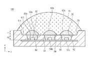
図1は本発明の第1実施形態による発光素子パッケージの斜視図であり、図2は図1の発光素子パッケージにおける個別レンズ、共通レンズ、及び樹脂物を除去した状態の斜視図であり、図3は図2の平面図である。 FIG. 1 is a perspective view of a light emitting device package according to a first embodiment of the present invention. FIG. 2 is a perspective view of the light emitting device package of FIG. 1 with an individual lens, a common lens, and a resin material removed. 3 is a plan view of FIG.
図1乃至図3を参照すると、第1実施形態の発光素子パッケージ100は、リセス(recess:凹み部あるいは窪み部)20及び複数の発光素子収容部(以下、“収容部”)30を含む胴体10、収容部30の内に個別的に位置する複数の発光素子50、第1電極41及び第2電極42、及び複数の個別レンズ60を含む。そして、複数の個別レンズ60を覆う共通レンズ70を含むことができる。
Referring to FIGS. 1 to 3, a light
これをより詳しく説明すれば、次の通りである。 This will be described in more detail as follows.
胴体10は、ポリフタルアミド(polyphthal amide:PPA)、液晶高分子(liquid crystal polymer:LCP)、ポリアミド9T(poly amid 9T:PA9T)のような樹脂、金属、感光性ガラス(photo sensitive glass)、サファイア(Al2O3)、セラミック、印刷回路基板(PCB)などを含むことができる。しかしながら、本実施形態がこのような物質に限定されるものではない。
The
このような胴体10は、発光素子パッケージ100の用途及び設計によって多様な形状を有することができる。一例に、胴体10の平面形状は、四角形、円形などの多様な形状を有することができる。
The
この胴体10には上部が開放されるリセス20が形成される。図面ではこのリセス20の平面形状を円形に図示したが、これに限定されるものではない。したがって、リセス20は四角形を含む多角形態の平面形状を有することもできる。
The
リセス20の側面はリセス20の底面に垂直または傾斜することができる。リセス20が傾斜した側面を有する場合、リセス20の側面と底面とがなす角度(図4のθ1、以下同一)は100〜170度でありうる。この際、角度(θ1)を120度以上にして、発光素子50から放出される光がよく反射されるようにすることができる。
The side surface of the
このリセス20の底面に収容部30が複数に形成される。この複数の収容部30は複数の発光素子50を個別的に収容するために形成される。図面では複数の収容部30の平面形状が円形状や、実施形態がこれに限定されるものではない。したがって、収容部30は四角形を含む多角形態の平面形状を有することもできる。
A plurality of
そして、収容部30の側面は収容部30の底面に対して垂直とするか、あるいは傾斜させることができる。収容部30が傾斜した側面を有する場合、収容部30の側面と底面とがなす角度(図4のθ2、以下同一)は100〜170度でありうる。この際、角度(θ2)を120度以上にして、発光素子50から放出される光がよく反射されるようにすることができる。
The side surface of the
このようなリセス20及び複数の収容部30を有する胴体10は複数の層を積層して形成されたり、射出成形などにより形成される。その他の多様な方法により胴体10を形成できることは勿論である。
The
このような胴体10には発光素子50に電気的に連結される第1電極41及び第2電極42が配置される。このような第1電極41及び第2電極42は所定の厚さを有する金属プレートで形成され、この表面に他の金属層がメッキされることもある。第1電極41及び第2電極42は伝導性に優れる金属で構成される。このような金属には、チタニウム(Ti)、銅(Cu)、ニッケル(Ni)、金(Au)、クロム(Cr)、タンタリウム(Ta)、白金(Pt)、スズ(Sn)、銀(Ag)などがある。
The
このような第1電極41及び第2電極42の一部は収容部30を通じて露出され、残りの部分は胴体10の内部を貫通して外部に露出される。本実施形態では、第1電極41及び第2電極42が収容部30の底面に接して形成されるが、これに限定されるものではない。したがって、第1電極41及び第2電極42がリセス20の底面に接して形成されたり、胴体10の上面に接して形成されることもできる。
A part of the
収容部30の内には第1電極41及び第2電極42と電気的に連結されながら発光素子50が位置する。発光素子50は、ワイヤ52を介したワイヤボンディングによって第1電極41及び第2電極42と電気的に連結されることもできる。
The
発光素子50は2つの電極層が上方に露出するように配置された水平型チップまたは2つの電極層が互いに発光層の反対側に位置した垂直型チップで構成される。この際、水平型チップは、第1電極41及び第2電極42にそれぞれワイヤ52により連結される。垂直型チップは、第1電極41及び第2電極42のうち、1つの電極には互いに接触して形成され、他の1つの電極にはワイヤ52により連結される。図2及び3では、一例として水平型チップを基準にして図示した。
The
しかしながら、実施形態がこれに限定されるものではない。即ち、ワイヤボンディングの以外にダイボンディング(die bonding)またはフリップチップ(flip chip)方式などにより発光素子50と第1及び第2電極41、42が電気的に連結される。
However, the embodiment is not limited to this. That is, in addition to wire bonding, the
そして、この収容部30の内に発光素子50を封入しながら樹脂物(図4の参照符号82、84、以下同一)が詰められる。この樹脂物82、84は、シリコンまたはエポキシのような透光性材料からなる。この樹脂物82、84は、発光素子50から放出された光を吸収して他の波長を放出する蛍光物質を含むことができる。
Then, a resin material (
この樹脂物82、84の上に凸形状の個別レンズ60が位置する。この個別レンズ60は樹脂などをモールディングして形成されたり、別途に製作されたレンズを付着して使用することができる。図面及び説明では樹脂物82、84と個別レンズ60とが互いに異なる構成であると図示及び説明するが、樹脂物82、84と個別レンズ60とを同一の工程で同時に形成することもできる。この個別レンズ60は、少なくとも一部分がリセス20の底面と接触することもできる。
A convex
この個別レンズ60を覆いながらリセス20の上に共通レンズ70が形成される。この共通レンズ70は樹脂などをモールディングして形成されたり、別途に製作されたレンズを付着して使用することができる。共通レンズ70が樹脂などにより構成された場合には蛍光物質を含むことができる。この共通レンズ70は個別レンズ60と離隔して配置されることもできる。
A
図4を参照して、本実施形態のリセス20、収容部30、発光素子50、個別レンズ60、共通レンズ70、及び樹脂物82、84についてより詳しく説明する。図4は、図1のIV−IV線に沿って切った断面図である。
With reference to FIG. 4, the
本実施形態において、1つのリセス20には複数の発光素子50a、50bを個別に収容する複数の収容部32、34が形成される。以下、複数の収容部32、34が第1収容部32及び第2収容部34を含むことを例示した。
In the present embodiment, a
ここで、樹脂物82、84に蛍光物質が含まれる場合には、十分な量の蛍光物質が含まれるように収容部32、34の深さ(H2)が発光素子50a、50bより大きいことがある。一例に、収容部32、34の深さ(H2)が発光素子50a、50bより少なくても30μm以上大きく形成される。そして、リセス20の深さ(H1)は、収容部32、34の深さ(H2)より小さいことがある。これは、リセス20の深さ(H1)が過度に大きくなると、反射により損失される光量が多くなるためである。
Here, when the
このように、本実施形態ではリセス20の深さ(H1)と収容部32、34の深さ(H2)を最適化して発光素子パッケージ100の効率向上により寄与することができる。
As described above, in this embodiment, the depth (H1) of the
複数の収容部32、34には複数の発光素子50a、50bが一対一対応して位置する。即ち、第1発光素子50aが第1収容部32に位置し、第2発光素子50bが第2収容部34に位置する。そして、第1収容部32の内には第1樹脂物82が位置し、第2収容部34の内には第2樹脂物84が位置する。
The plurality of
この際、第1及び第2発光素子50a、50bは、同一の波長の光を放出する同種の発光素子であることもあり、互いに異なる波長の光を放出する異種の発光素子であることもある。第1樹脂物82、第2樹脂物84、及び共通レンズ70の蛍光物質も互いに同一の種類の蛍光物質であることもあり、互いに異なる種類の蛍光物質であることもある。蛍光物質には、サルファイド系、シリケート系、イットリウム−アルミニウム−ガーネット(YAG)系、窒酸化物係、窒化物系などの多様な蛍光物質を使用することができる。
At this time, the first and second
一例に、第1及び第2発光素子50a、50bが青色光を放出する発光素子であり、第1及び第2樹脂物82、84の蛍光物質が黄色光を放出する蛍光物質(以下、“黄色蛍光物質”)でありうる。
For example, the first and second
他の例に、第1及び第2発光素子50a、50bは青色光を放出する発光素子であり、第1樹脂物82の蛍光物質が黄色蛍光物質であり、第2樹脂物84の蛍光物質が緑色光を放出する蛍光物質(以下、“緑色光物質”)でありうる。この際、第1発光素子50aと黄色蛍光物質との組合が第2発光素子50bと緑色蛍光物質との組合より効率に優れることがある。そして、共通レンズ70の蛍光物質が赤色光を放出する蛍光物質(以下、“赤色蛍光物質”)でありうる。
In another example, the first and second
即ち、従来には1つの樹脂物のみを使用し、複数の発光素子50a、50bに互いに異なる樹脂物を使用することが不可能であった。本実施形態では、第1及び第2発光素子50a、50bを個別的に第1及び第2収容部32、34に位置させるので、第1及び第2樹脂物82、84の蛍光物質を互いに異なる物質で形成することも可能である。これによって、第1及び第2発光素子50a、50bの特性を考慮して蛍光物質を使用することができる。
That is, conventionally, it has been impossible to use only one resin material and use different resin materials for the plurality of
また、異種の蛍光物質を異なる空間である各収容部32、34又は/及びリセス20に位置するようにすることができるので、異種の蛍光物質を混合して発生する問題を防止することができる。例えば、赤色蛍光物質が他の蛍光物質と混合される場合、赤色蛍光物質が他の蛍光物質から変換された波長の光を吸収して全体的に輝度と効率を低下させることがある。本実施形態では、このような赤色蛍光物質を他の蛍光物質と他の空間に位置させて輝度の低下を防止することができる。
In addition, since different types of fluorescent materials can be positioned in the respective
第1収容部32の上に第1個別レンズ60aが位置し、第2収容部34の上に第1個別レンズ60aと離隔する第2個別レンズ60bが位置する。本実施形態において、第1及び第2個別レンズ60a、60bはリセス20の側面で一定間隔離隔して形成され、各発光素子50a、50bの上で凸形状を有することができる。
The first
従来のように、複数の発光素子50a、50bに対応するレンズを1つのレンズのみで形成する場合、レンズの表面が緩やかな曲面からなる。これによって、レンズの表面で全反射が多く発生して効率が減少する。一方、本実施形態のように、第1及び第2発光素子50a、50bの各々に対応するように第1及び第2個別レンズ60a、60bを備える場合には、レンズの表面が比較的大きい曲率を有することができるので、全反射を減らすことができ、これによって効率を向上させることができる。
When the lenses corresponding to the plurality of
この際、第1及び第2個別レンズ60a、60bは効率を考慮して略半球形の形状を有することができる。従来のように複数の発光素子50a、50bに1つのレンズを使用する場合には、半球形のレンズを使用すれば、発光素子パッケージ100の厚さが厚過ぎるようになることがあるので、半球形のレンズを使用することができなかった。一方、本実施形態では第1及び第2個別レンズ60a、60bを備えて効率の面で優れる半球形の形状を有することができる。
At this time, the first and second
また、第1及び第2個別レンズ60a、60bを備えるので、第1及び第2発光素子50a、50bの特性を考慮して第1及び第2個別レンズ60a、60bの形状、材質などを互いに異なるようにすることができる。これによって、多様な構造の発光素子パッケージ100を形成することができる。第1及び第2個別レンズ60a、60bの形状、材質などを異なるようにした実施形態は、図22乃至図25を参照して後述する。
In addition, since the first and second
この第1個別レンズ60a及び第2個別レンズ60bを覆いながら共通レンズ70が形成される。この共通レンズ70の屈折率を第1及び第2個別レンズ60a、60bより小さくして光抽出効率をより向上することができる。即ち、光が高い屈折率の物質から低い屈折率の物質に通過するようにして、フレネル(Fresnel)反射などによる損失を最小化することができる。
A
このように、本実施形態では各発光素子50a、50bの特性を考慮して多様な発光素子パッケージ100を製造することができ、発光素子パッケージ100の効率を向上することができる。
As described above, in the present embodiment, various light emitting device packages 100 can be manufactured in consideration of the characteristics of the
前述した第1実施形態において、個別レンズ又は/及び共通レンズの形状を変形した変形例を図5乃至図11を参照して説明する。明確な説明のために、第1実施形態と同一または極めて類似の構成に対しては詳細な説明を省略し、互いに異なる構成に対してのみ詳しく説明する。 In the first embodiment described above, a modified example in which the shape of the individual lens and / or the common lens is modified will be described with reference to FIGS. For the sake of clarity, detailed description will be omitted for configurations that are the same as or very similar to those of the first embodiment, and only different configurations will be described in detail.
図5は、本発明の第1実施形態の第1変形例による発光素子パッケージの断面図である。 FIG. 5 is a cross-sectional view of a light emitting device package according to a first modification of the first embodiment of the present invention.
図5を参照すると、本変形例では、個別レンズ602の上部に凹部602aが形成される。このような凹部602aはリセス20の底面に向けて凹まれた形態を有しており、個別レンズ602の他の部分と緩やかな曲面をなしながら連結される。このような凹部602aは、光が個別レンズ602の周辺部を通じて外部に放出されるように誘導する。即ち、このような個別レンズ602を使用して指向角を広げることができる。
Referring to FIG. 5, in the present modification, a
図6は、本発明の第1実施形態の第2変形例による発光素子パッケージの断面図である。 FIG. 6 is a cross-sectional view of a light emitting device package according to a second modification of the first embodiment of the present invention.
図6を参照すると、本変形例の発光素子パッケージにおいて、個別レンズ602は上部に凹部602aが形成され、この凹部602aの内に反射物質604が形成される。この反射物質604は、個別レンズ602の上面の5乃至60%の面積に位置することができる。
Referring to FIG. 6, in the light emitting device package of the present modification, the
このように、凹部602aの内に位置した反射物質604は、発光素子50から放出された光、または収容部30の側面または底面で反射された光のうち、凹部602aに進行する光を反射する。これによって、発光素子50から放出された光、または収容部30の側面または底面で反射された光は凹部602aが形成されない部分を通じて外部に放出される。これによって、光が個別レンズ602の周辺部を通じて外部に放出されるため、広い指向角の光を提供することができる。
As described above, the
例えば、上記反射物質604は、透過率が70%以上の有機物に光を反射または散乱させることができる無機物を混合して凹部602aの上に形成される。無機物は、TiO2、SiO2、Al、Al2O3、Agのうち、少なくともいずれか1つを含むことができる。有機物と無機物との配合比によって光を全反射したり一部反射することができ、有機物と無機物との配合比は1:0.001〜1:1となることもできる。
For example, the
また、例えば、反射物質604は、SiO2、TiO2、Al、Ag、Tiのうち、少なくともいずれか1つで形成された蒸着膜でありうる。この蒸着膜は100Å以上の厚さで形成される。
For example, the
本実施形態による発光素子パッケージは、発光素子50と垂直方向にオーバーラップする領域の個別レンズ602に凹部602aを形成し、この凹部602aに反射物質604を形成することで、発光素子50から放出される光の指向角を調節することができる。
In the light emitting device package according to the present embodiment, the
図7は、本発明の第1実施形態の第3変形例による発光素子パッケージの断面図である。 FIG. 7 is a cross-sectional view of a light emitting device package according to a third modification of the first embodiment of the present invention.
図7を参照すると、本変形例において、個別レンズ606は表面に一定のパターン、一例として凹凸が形成される。このパターンは発光素子50から放出された光が透過または反射される時、この光を屈折または分散させる。これによって、個別レンズ606の中央部と側面部の光が均一な光度の分布を有することができる。また、個別レンズ606の中央部と側面部との間の色ばらつきを減少させることができる。
Referring to FIG. 7, in this modification, the
図8は、本発明の第1実施形態の第4変形例による発光素子パッケージの断面図である。 FIG. 8 is a cross-sectional view of a light emitting device package according to a fourth modification of the first embodiment of the present invention.
図8を参照すると、本変形例の発光素子パッケージにおいて、個別レンズ608は四角レンズからなる。このように、本変形例では多様な形状の個別レンズ608を使用することができる。
Referring to FIG. 8, in the light emitting device package of this modification, the
図9は、本発明の第1実施形態の第5変形例による発光素子パッケージの断面図である。 FIG. 9 is a cross-sectional view of a light emitting device package according to a fifth modification of the first embodiment of the present invention.
図9を参照すると、本変形例の発光素子パッケージにおける個別レンズ610は四角レンズから構成され、この個別レンズ610にマイクロレンズ610aが形成される。図9では、一例に、マイクロレンズ610aの断面が三角形状であると図示したが、本変形例がこれに限定されるものではない。したがって、マイクロレンズ601aは、円形、楕円形、または多角形の断面を有することができる。
Referring to FIG. 9, the
このようなマイクロレンズ610aを備えた個別レンズ610は、発光素子50から放出された光を屈折させて混色を容易にすることができる。
The
図10は、本発明の第1実施形態の第6変形例による発光素子パッケージの断面図である。 FIG. 10 is a cross-sectional view of a light emitting device package according to a sixth modification of the first embodiment of the present invention.
図10を参照すると、本変形例の発光素子パッケージにおいて、個別レンズ612は四角レンズであり、その上部に凹部612aが形成される。このような凹部612aにより発光素子50から放出された光の指向角を広げることができる。
Referring to FIG. 10, in the light emitting device package of the present modification, the
図11は、本発明の第1実施形態の第7変形例による発光素子パッケージの断面図である。 FIG. 11 is a cross-sectional view of a light emitting device package according to a seventh modification of the first embodiment of the present invention.
図11を参照すると、本変形例の発光素子パッケージでは共通レンズ72が四角レンズに形成される。このように、本変形例では多様な形状の共通レンズ72を使用することができる。このような共通レンズ72に、図9に図示したようなマイクロレンズを形成したり、図10に図示したような凹部を形成することもできる。
Referring to FIG. 11, in the light emitting device package of this modification, the
前述した第1実施形態において、蛍光物質の配置構造を変形した変形例を図12乃至図14を参照して説明する。明確な説明のために、第1実施形態と同一または極めて類似の構成に対しては詳細な説明を省略し、互いに異なる構成に対してのみ詳しく説明する。 In the first embodiment described above, a modification example in which the arrangement structure of the fluorescent material is modified will be described with reference to FIGS. For the sake of clarity, detailed description will be omitted for configurations that are the same as or very similar to those of the first embodiment, and only different configurations will be described in detail.
図12は、本発明の第1実施形態の第8変形例による発光素子パッケージの断面図である。 FIG. 12 is a cross-sectional view of a light emitting device package according to an eighth modification of the first embodiment of the present invention.
図12を参照すると、本変形例は発光素子50の上に蛍光物質を含むフィルム802が塗布されるということから、収容部30の内部を蛍光物質を含む樹脂で詰める第1実施形態と差がある。
Referring to FIG. 12, in this modification, since a
フィルム802は、透光性フィルムに蛍光物質が含まれて形成される。この透光性フィルムは、ポリカーボネート、ポリメチルメタクリレート、ポリプロピレン、石英、ガラスなどの透明な物質からなることができる。蛍光物質には、サルファイド系、シリケート系、イットリウム−アルミニウム−ガーネット(YAG)系、窒酸化物係、窒化物系などが使われる。
The
このようなフィルム802を使用すれば、蛍光物質を発光に寄与できる発光素子50の上で均一に分布させることができる。
If such a
図13は、本発明の第1実施形態の第9変形例による発光素子パッケージの断面図である。 FIG. 13 is a cross-sectional view of a light emitting device package according to a ninth modification of the first embodiment of the present invention.
図13を参照すると、本変形例は発光素子50の上に蛍光物質を含むフィルム802が塗布され、収容部30の内部の他の空間が樹脂物804で詰められる。このような樹脂物804は、エポキシ、シリコンなどを含むことができる。このような樹脂物804によりフィルム802がより安定的に発光素子50の上に配置される。
Referring to FIG. 13, in the present modification, a
図14は、本発明の第1実施形態の第10変形例による発光素子パッケージの断面図である。 FIG. 14 is a cross-sectional view of a light emitting device package according to a tenth modification of the first embodiment of the present invention.
図14を参照すると、本変形例では、収容部302の上部に段差302aが形成され、この段差302aに蛍光物質を含むフィルム802が提供される。本変形例では、収容部302の上部に段差302aが形成されて、この段差302aにフィルム802が安定的に固定される。
Referring to FIG. 14, in this modification, a
この段差302aは、フィルム802の厚さと実質的に同一の深さを有することができる。しかしながら、本実施形態がこれに限定されるものではなく、段差302aの深さがフィルム802の厚さより薄いか厚いものも可能である。
The
図14ではフィルム802の下の空間が空いているものと図示したが、図13のようにこの空間に樹脂物を形成できることは勿論である。
Although FIG. 14 shows that the space under the
前述した第1実施形態において、胴体を変形した変形例を図15乃至図19を参照して説明する。明確な説明のために、第1実施形態と同一または極めて類似の構成に対しては詳細な説明を省略し、互いに異なる構成に対してのみ詳しく説明する。 Modification examples in which the body is modified in the first embodiment described above will be described with reference to FIGS. 15 to 19. For the sake of clarity, detailed description will be omitted for configurations that are the same as or very similar to those of the first embodiment, and only different configurations will be described in detail.
図15は本発明の第1実施形態の第11変形例による発光素子パッケージの断面図であり、図16は本発明の第1実施形態の第11変形例による発光素子パッケージの平面図である。図17及び図18は、本発明の第1実施形態の第11変形例の他の例を示す平面図である。 15 is a cross-sectional view of a light emitting device package according to an eleventh modification of the first embodiment of the present invention, and FIG. 16 is a plan view of a light emitting device package according to an eleventh modification of the first embodiment of the present invention. 17 and 18 are plan views showing other examples of the eleventh modification of the first embodiment of the present invention.
図15を参照すると、本変形例による胴体10は個別レンズ60をガイド及び固定するガイド部材102を備える。このようなガイド部材102は、別途の工程により製作されて胴体10に付着することができる。または、胴体10を形成する射出工程などで、ガイド部材102と胴体10とを一体形成することもできる。
Referring to FIG. 15, the
図16を参照すると、ガイド部材102は個別レンズ60の縁に沿って形成される閉曲線の形状を備えることができる。本変形例では、個別レンズ60の平面形状が円形に形成されてガイド部材102が環状からなることができる。個別レンズ60の平面形状が四角の場合にはガイド部材もこれによって個別レンズ60に対応する部分が開いた四角形に形成される。
Referring to FIG. 16, the
このようなガイド部材102によって個別レンズ60が発光素子50の上で、効率を極大化することができる位置に形成される。
By such a
図16では、複数の個別レンズ60をガイド(案内)するガイド部材102が1つに連結されているものが図示されているが、本発明がこれに限定されるものではない。したがって、図17のように、それぞれの個別レンズ60をガイドするガイド部材104が互いに離隔して形成されることも可能である。
In FIG. 16, the
また、図18に示すように、ガイド部材106が個別レンズ60の間で一字形状に形成されることもできる。ガイド部材106は、その他に多様な平面形状を有することができることは勿論である。
Further, as shown in FIG. 18, the
図19は、本発明の第1実施形態の第12変形例による発光素子パッケージの断面図である。 FIG. 19 is a cross-sectional view of a light emitting device package according to a twelfth modification of the first embodiment of the present invention.
図19を参照すると、本変形例の胴体10aは、上部に共通レンズ74を固定するための段差108を備える。図19では、共通レンズ74として別途に製作レンズを使用し、共通レンズ74の下部のリセス20の空間を樹脂物88で詰めた例が図示された。この樹脂物88に蛍光物質が含まれる。
Referring to FIG. 19, the
このような段差108により共通レンズ74を所望の位置に強固に固定することができる。
Such a
前述した第1実施形態において、第1電極及び第2電極を変形した変形例を図20を参照して説明する。 In the first embodiment described above, a modification in which the first electrode and the second electrode are modified will be described with reference to FIG.
図20は、本発明の第1実施形態の第13変形例による発光素子パッケージの断面図である。 FIG. 20 is a cross-sectional view of a light emitting device package according to a thirteenth modification of the first embodiment of the present invention.
図20を参照すると、本実施形態の第1電極41は、複数の発光素子50にそれぞれ対応する複数の電極部41a、41bを具備し、第2電極42も複数の発光素子50に対応する複数の電極部42a、42bを具備する。これによって、複数の発光素子50を互いに別に駆動することができる。
Referring to FIG. 20, the
以下、図21を参照して、第2実施形態による発光素子パッケージを説明する。図21は、本発明の第2実施形態による発光素子パッケージの断面図である。 Hereinafter, the light emitting device package according to the second embodiment will be described with reference to FIG. FIG. 21 is a cross-sectional view of a light emitting device package according to a second embodiment of the present invention.
本実施形態では、1つのリセス20に3個の収容部32、34、36、3個の発光素子50a、50b、50c、及び3個の個別レンズ60a、60b、60cが位置する。
In the present embodiment, three
図21には3個の収容部32、34、36が1つの列を成して形成されるものを図示したが、実施形態がこれに限定されるものではない。したがって、4個以上の収容部が形成され、これらが多角形構造をなしながら配置されたり、2つ以上の列を成して配置される。
Although FIG. 21 illustrates the case where the three
ここで、第1乃至第3発光素子50a、50b、50cは同一の波長の光を放出する同種の発光素子であることもあり、互いに異なる波長の光を放出する異種の発光素子であることもある。第1、第2、及び/又は第3樹脂物82、84、86の蛍光物質も互いに同一の種類の蛍光物質であることもあり、互いに異なる種類の蛍光物質であることもある。
Here, the first to third
一例に、第1乃至第3発光素子50a、50b、50cが青色光を放出する発光素子であり、第1乃至第3樹脂物82、84、86の蛍光物質が黄色蛍光物質でありうる。
For example, the first to third light emitting
他の例に、第1乃至第3発光素子50a、50b、50cが青色光を放出する発光素子であり、第1乃至第3樹脂物82、84、86の蛍光物質が緑色蛍光物質及び赤色蛍光物質を共に含むことができる。
In another example, the first to third light emitting
更に他の例に、第1乃至第3発光素子50a、50b、50cが青色光を放出する発光素子であり、第1乃至第3樹脂物82、84、86の蛍光物質が緑色蛍光物質、赤色蛍光物質、及び黄色蛍光物質を共に含むことができる。
In still another example, the first to third
更に他の例に、第1乃至第3発光素子50a、50b、50cが青色光を放出する発光素子であり、第1、第2、及び第3樹脂物82、84、86の蛍光物質がそれぞれ黄色、緑色、及び赤色蛍光物質でありうる。この際、第1発光素子50aと黄色蛍光物質との組合の効率が最も高く、第3発光素子50cと赤色蛍光物質との組合の効率が最も低いことがある。
In still another example, the first to third
更に他の例に、第1発光素子50aが緑色光を放出する発光素子であり、第2発光素子50bが青色光を放出する発光素子であり、第3発光素子50cが赤色光を放出する発光素子でありうる。この際、第1及び第3樹脂物82、86には蛍光物質が含まれず、第2樹脂物84は黄色蛍光物質を含むことができる。この際、第1発光素子50aの効率が最も高く、第2発光素子50bと黄色蛍光物質との組合の効率がその次に高く、第3発光素子50cの効率が最も低いことがある。
In still another example, the first
更に他の例に、第1乃至第3発光素子50a、50b、50cが紫外線(UV)を放出する発光素子であり、第1、第2、及び第3樹脂物82、84、86の蛍光物質がそれぞれ黄色、緑色、及び赤色の光を放出する蛍光物質でありうる。この際、第1発光素子50aと黄色蛍光物質との組合の効率が最も高く、第3発光素子50cと赤色蛍光物質との組合の効率が最も低いことがある。
In another example, the first to third
その他にも、多様な組合の発光素子及び蛍光物質が使用できることは勿論である。 Of course, various combinations of light emitting elements and fluorescent materials can be used.
以下、第3実施形態及びその変形例による発光素子パッケージを図22乃至25を参照して説明すれば、次の通りである。 Hereinafter, a light emitting device package according to the third embodiment and its modification will be described with reference to FIGS.
図22は、本発明の第3実施形態による発光素子パッケージを示す断面図である。図23は、本発明の第3実施形態の第1変形例による発光素子パッケージを示す断面図である。 FIG. 22 is a cross-sectional view illustrating a light emitting device package according to a third embodiment of the present invention. FIG. 23 is a cross-sectional view showing a light emitting device package according to a first modification of the third embodiment of the present invention.
図22を参照すると、本実施形態では、第1個別レンズ614aと第2個別レンズ614bとが互いに異なる形状を有する。一例に、第1及び第2個別レンズ614a、614bの直径及び高さを異にして曲率が互いに異なる場合を例示する。これは、第1発光素子50aの効率が第2発光素子50bの効率と異なることを考慮したものである。
Referring to FIG. 22, in the present embodiment, the first
ここで、第1発光素子50aの効率とは、第1樹脂物32に蛍光物質が含まれた場合には第1発光素子50aと蛍光物質との組合による効率を意味し、第1樹脂物32に蛍光物質が含まれていない場合には第1発光素子50aの効率を意味する。同様に、第2発光素子50bの効率とは、第2樹脂物34に蛍光物質が含まれた場合には第2発光素子50bと蛍光物質との組合による効率を意味し、第2樹脂物34に蛍光物質が含まれていない場合には第2発光素子50bの効率を意味する。
Here, the efficiency of the first
本実施形態では、第1発光素子50aの効率が第2発光素子50bの効率より大きい場合を例示する。この際、第1発光素子50aに対応する第1個別レンズ614aより第2発光素子50bに対応する第2個別レンズ614bが半球形に近い形態に形成される。
In this embodiment, the case where the efficiency of the 1st
このように、第2個別レンズ614bが半球形に一層近い形態に形成されるので、光抽出効率が第1個別レンズ614aより優れる。これによって、相対的に低い第2発光素子50bの効率を補償することができる。これによって、第1及び第2発光素子50a、50bの互いに異なる効率を均一化させることができる。
Thus, since the second
より具体的に、第2個別レンズ614bが略半球形であるので、高さ(T2)に対する直径(W2)の比率が約2である。そして、第1個別レンズ614aの直径(W1)は第2個別レンズ614bの直径(W2)と同一であり、高さ(T1)が第2個別レンズ614bの高さ(T2)より小さいことがある。これによると、第1個別レンズ614aの高さ(T1)に対する直径(W1)の比率が2より大きい値を有する。
More specifically, since the second
即ち、第2個別レンズ614bの高さ(T2)に対する直径(W2)の比率が第1個別レンズ614aの高さ(T1)に対する直径(W1)の比率より2に近いことがある。
That is, the ratio of the diameter (W2) to the height (T2) of the second
図22には第1個別レンズ614aの高さ(T1)を第2個別レンズ614bの高さ(T2)より小さくしたものを例示したが、本実施形態がこれに限定されるものではない。したがって、図23に示すように、第1個別レンズ614cの高さ(T3)を第2個別レンズ614bの高さ(T2)より大きくすることも可能である。これによると、第1個別レンズ614cの高さ(T3)に対する直径(W1)の比率が2より小さな値を有する。したがって、第2個別レンズ614bの高さ(T2)に対する直径(W2)の比率が第1個別レンズ614cの高さ(T3)に対する直径(W1)の比率より2に近いことがある。
Although FIG. 22 illustrates an example in which the height (T1) of the first
また、図示してはいないが、個別レンズの幅を異にして互いに異なる光抽出効率を有する個別レンズを形成することも可能である。 Although not shown, it is also possible to form individual lenses having different light extraction efficiencies with different widths of the individual lenses.
このように、本実施形態では各発光素子50a、50bに対応してそれぞれ個別レンズ614a、614bを形成して、各個別レンズ614a、614bの形状を互いに異なるようにすることができる。これによって、各発光素子50a、50bの互いに異なる特性を補償して光が均一に放出できるようにする。
Thus, in this embodiment, the
図24は、本発明の第3実施形態の第2変形例による発光素子パッケージを示す断面図である。 FIG. 24 is a cross-sectional view showing a light emitting device package according to a second modification of the third embodiment of the present invention.
本変形例では、第1発光素子50aに対応する第1個別レンズ616aと第2発光素子50bに対応する第2個別レンズ616bとを互いに異なる物質で構成する。
In this modification, the first
第1発光素子50aの効率が第2発光素子50bの効率より高い場合を例示する。この際、第1個別レンズ616aは屈折率が1.4以上で、かつ1.5未満の物質からなり、第2個別レンズ616bは屈折率が1.5以上で、かつ1.6未満の物質からなることができる。このような第1及び第2個別レンズ616a、616bは多様な物質で構成される。
The case where the efficiency of the 1st
一般に、屈折率が1.4帯の物質より屈折率が1.5の物質でレンズを形成した場合に光抽出効率が高い。したがって、屈折率が1.5帯の物質から構成された第2個別レンズ616bの光抽出効率が第1個別レンズ616aの光抽出効率より高い。これによって、第1及び第2発光素子50a、50bの効率の差を補償することができる。
In general, light extraction efficiency is higher when a lens is formed of a material having a refractive index of 1.5 than a material having a refractive index of 1.4. Therefore, the light extraction efficiency of the second
上記では、一例として特定の屈折率を提示したが、本変形例がこれに限定されるものではない。即ち、光抽出効率の高いレンズを相対的に効率の低い第2発光素子50bの上に形成し、光抽出効率の低いレンズを相対的に効率の高い第1発光素子50aの上に形成すればよい。
In the above, a specific refractive index is presented as an example, but the present modification is not limited thereto. That is, if a lens having a high light extraction efficiency is formed on the second
図25は、本発明の第3実施形態の第3変形例による発光素子パッケージを示す断面図である。 FIG. 25 is a cross-sectional view showing a light emitting device package according to a third modification of the third embodiment of the present invention.
図25を参照すると、第1個別レンズ618aが凸形状のレンズからなり、第2個別レンズ618bが上部に形成された凹部に反射物質620が詰められたレンズからなる。このように、本変形例では、互いに異なる構造の個別レンズ618a、618bを共に使用する。本変形例は、図25に図示された場合に限定されるものではない。したがって、個別レンズ618a、618bには、図4乃至図10に示す個別レンズを自由に使用することができる。
Referring to FIG. 25, the first
前述した実施形態及び変形例による発光素子パッケージは、バックライトユニット、指示装置、ランプ、街灯のような照明システムとして機能することができる。これを図26及び図27を参照して説明する。 The light emitting device package according to the embodiment and the modification described above can function as an illumination system such as a backlight unit, a pointing device, a lamp, and a streetlight. This will be described with reference to FIGS.
図26は、本発明の実施形態による発光素子パッケージを含むバックライトユニットを説明する図である。但し、図26のバックライトユニット1100は照明システムの一例であり、これに限定されるものではない。
FIG. 26 is a view illustrating a backlight unit including a light emitting device package according to an embodiment of the present invention. However, the
図26を参照すると、バックライトユニット1100は、ボトムカバー1140、このボトムカバー1140の内に配置された光ガイド部材1120、及びこの光ガイド部材1120の少なくとも一側面または下面に配置された発光モジュール1110を含むことができる。また、光ガイド部材1120の下には反射シート1130が配置される。
Referring to FIG. 26, the
ボトムカバー1140は、光ガイド部材1120、発光モジュール1100、及び反射シート1130が収納できるように上面が開口されたボックス(box)形状に形成され、金属または樹脂で形成される。しかしながら、これに限定されるものではない。
The
発光モジュール1110は、基板700に搭載された複数の発光素子パッケージ600を含むことができる。複数の発光素子パッケージ600は、光ガイド部材1120に光を提供する。
The
図示したように、発光モジュール1110は、ボトムカバー1140の内側面のうち、少なくともいずれか1つに配置され、これによって、光ガイド部材1120の少なくとも1つの側面に向けて光を提供することができる。
As illustrated, the
但し、発光モジュール1110は、ボトムカバー1140の内で光ガイド部材1120の下に配置されて、光ガイド部材1120の下面に向けて光を提供することもできる。これは、バックライトユニット1100の設計によって多様に変形可能である。
However, the
光ガイド部材1120は、ボトムカバー1140の内に配置される。光ガイド部材1120は、発光モジュール1110から提供された光を面光源化して、表示パネルにガイドすることができる。
The
このような光ガイド部材1120は、例えば、導光板(light guide panel:LGP)でありうる。この導光板は、例えば、ポリメチルメタアクリレート(polymethyl metaacrylate:PMMA)のようなアクリル樹脂、ポリエチレンテレフタレート(polyethylene terephthalate:PET)、環状オレフィン共重合体(COC)、ポリカーボネート(polycarbonate:PC)、ポリエチレンナフタレート(polyethylene naphthalate)樹脂のうちの1つで形成される。
For example, the
この光ガイド部材1120の上側に光学シート1150が配置される。
An
この光学シート1150は、例えば、拡散シート、集光シート、輝度上昇シート、及び蛍光シートのうち、少なくとも1つを含むことができる。例えば、光学シート1150が拡散シート、集光シート、輝度上昇シート、及び蛍光シートが積層されて形成される。この場合、拡散シート1150は、発光モジュール1110から出射された光を均等に拡散させ、この拡散された光が集光シートにより表示パネルに集光される。この際、集光シートから出射される光はランダムに偏光された光である。輝度上昇シートは、集光シートから出射された光の偏光度を増加させることができる。集光シートは、例えば、水平又は/及び垂直プリズムシートでありうる。そして、輝度上昇シートは、例えば、照度強化フィルム(dual brightness enhancement film)でありうる。また、蛍光シートは蛍光体が含まれた透光性プレートまたはフィルムでありうる。
The
光ガイド部材1120の下には反射シート1130が配置される。反射シート1130は、光ガイド部材1120の下面を通じて放出される光を光ガイド部材1120の出射面に向けて反射することができる。この反射シート1130は、反射率の良い樹脂、例えば、PET、PC、ポリビニールクロライド(poly vinyl chloride)、レジンなどで形成されるが、これに限定されるものではない。
A
図27は、本発明の実施形態による発光素子パッケージを含む照明システムを説明する図である。但し、図27の照明システム1200は照明システムの一例であり、これに対して限定するものではない。
FIG. 27 is a view illustrating a lighting system including a light emitting device package according to an embodiment of the present invention. However, the
図27を参照すると、照明システム1200は、ケース胴体1210、このケース胴体1210に設置された発光モジュール1230、及びケース胴体1210に設置され、外部電源から電源が提供される連結端子1220を含むことができる。
Referring to FIG. 27, the
ケース胴体1210は、放熱特性の良好な物質で形成されることが好ましく、例えば金属または樹脂で形成される。
The
発光モジュール1230は、基板700及び該基板700に搭載される少なくとも1つの発光素子パッケージ600を含むことができる。
The
上記基板700は絶縁体に回路パターンが印刷されたものであることがあり、例えば、一般印刷回路基板(printed circuit board:PCB)、メタルコア(metal core)PCB、軟性(flexible)PCB、セラミックPCBなどを含むことができる。
The
また、基板700は光を効率的に反射する物質で形成されたり、表面が光が効率的に反射されるカラー、例えば白色、銀色などで形成される。
In addition, the
基板700の上には少なくとも1つの発光素子パッケージ600が搭載される。
At least one light emitting
発光素子パッケージ600は、各々少なくとも1つの発光素子(LED:Light Emitting Diode)を含むことができる。発光素子は。赤色、緑色、青色、または白色の有色光を各々発光する有色発光素子及び紫外線(UV:Ultra Violet)を発光するUV発光素子を含むことができる。 Each of the light emitting device packages 600 may include at least one light emitting diode (LED). The light emitting element. A colored light emitting element that emits red, green, blue, or white colored light and a UV light emitting element that emits ultraviolet (UV) light can be included.
発光モジュール1230は、色感及び輝度を得るために多様な発光素子の組合を有するように配置される。例えば、高演色性(CRI)を確保するために、白色発光素子、赤色発光素子、及び緑色発光素子を組合せて配置することができる。また、発光モジュール1230から放出される光の進行経路上には蛍光シートがさらに配置され、蛍光シートは上記発光モジュール1230から放出される光の波長を変化させる。例えば、発光モジュール1230から放出される光が青色波長帯を有する場合、蛍光シートには黄色蛍光体が含まれ、発光モジュール1230から放出された光は上記蛍光シートを経て最終的に白色光と見えるようになる。
The
連結端子1220は、発光モジュール1230と電気的に連結されて電源を供給することができる。図27の図示によると、連結端子1220はソケット方式により外部電源に螺合されるが、これに対して限定するものではない。例えば、連結端子1220はピン(pin)形態に形成されて外部電源に挿入されたり、配線により外部電源に連結されることもできる。
The
前述したような照明システムは、上記発光モジュールから放出される光の進行経路上に、光ガイド部材、拡散シート、集光シート、輝度上昇シート、及び蛍光シートのうち、少なくともいずれか1つが配置されて、所望の光学的効果を得ることができる。 In the illumination system as described above, at least one of a light guide member, a diffusion sheet, a condensing sheet, a brightness enhancement sheet, and a fluorescent sheet is disposed on a travel path of light emitted from the light emitting module. Thus, a desired optical effect can be obtained.
以上、説明したように、照明システムは、光効率が向上し、均一な光を放出する発光素子パッケージを含むことで、優れる光効率及び特性を有することができる。 As described above, the illumination system can have excellent light efficiency and characteristics by including a light emitting device package that improves light efficiency and emits uniform light.
以上、実施形態に説明された特徴、構造、効果などは、本発明の少なくとも1つの実施形態に含まれ、必ず1つの実施形態のみに限定されるのではない。延いては、各実施形態で例示された特徴、構造、効果などは、実施形態が属する分野の通常の知識を有する者により他の実施形態に対しても組合または変形されて実施可能である。したがって、このような組合と変形に関連した内容は本発明の範囲に含まれることと解釈されるべきである。 As described above, the features, structures, effects, and the like described in the embodiments are included in at least one embodiment of the present invention, and are not necessarily limited to only one embodiment. As a result, the features, structures, effects, and the like exemplified in each embodiment can be combined or modified with respect to other embodiments by a person having ordinary knowledge in the field to which the embodiment belongs. Therefore, contents related to such combinations and modifications should be construed as being included in the scope of the present invention.
以上、本発明を好ましい実施形態をもとに説明したが、これは単なる例示であり、本発明を限定するのでない。本発明の本質的な特性を逸脱しない範囲内で、多様な変形及び応用が可能であることが同業者にとって明らかである。例えば、実施形態に具体的に表れた各構成要素は変形して実施することができ、このような変形及び応用にかかわる差異点も、特許請求の範囲で規定する本発明の範囲に含まれるものと解釈されるべきである。
As mentioned above, although this invention was demonstrated based on preferable embodiment, this is only an illustration and does not limit this invention. It will be apparent to those skilled in the art that various modifications and applications can be made without departing from the essential characteristics of the invention. For example, each component specifically shown in the embodiment can be modified and implemented, and such differences in modification and application are also included in the scope of the present invention defined in the claims. Should be interpreted.
Claims (15)
前記リセスの底面に配置された第1及び第2発光素子収容部を含む胴体と、
前記第1発光素子収容部に提供された第1発光素子と、
前記第2発光素子収容部に提供された第2発光素子と、
前記第1発光素子の上に配置された第1個別レンズと、
前記第2発光素子の上に配置された第2個別レンズと、
前記第1個別レンズ及び前記第2個別レンズを覆う共通レンズと、を含み、
前記第2個別レンズの屈折率は、前記第1個別レンズの屈折率より大きく、
前記第2個別レンズを介した光抽出効率が、前記第1個別レンズを介した光抽出効率より大きく、
前記第1発光素子の発光効率は、前記第2発光素子の発光効率より大きく、
前記第1発光素子の発光効率と前記第2発光素子の発光効率との間の差が、前記第1個別レンズを介した光抽出効率と前記第2個別レンズを介した光抽出効率との間の差によって補償され、前記第1個別レンズ及び前記第2個別レンズのそれぞれを介して抽出された光が、前記共通レンズの外部に均一に放出されることを特徴とする発光素子パッケージ。 Recess and
A fuselage including first and second light emitting element receiving portions disposed on a bottom surface of the recess;
A first light emitting device provided in the first light emitting device housing;
A second light emitting device provided in the second light emitting device housing;
A first individual lens disposed on the first light emitting element;
A second individual lens disposed on the second light emitting element;
A common lens covering the first individual lens and the second individual lens,
The refractive index of the second individual lens is greater than the refractive index of the first individual lens,
The light extraction efficiency through the second individual lens is greater than the light extraction efficiency through the first individual lens;
The luminous efficiency of the first light emitting element is greater than the luminous efficiency of the second light emitting element,
The difference between the light emission efficiency of the first light emitting element and the light emission efficiency of the second light emitting element is between the light extraction efficiency through the first individual lens and the light extraction efficiency through the second individual lens. A light emitting device package , wherein light extracted through each of the first individual lens and the second individual lens is uniformly emitted to the outside of the common lens .
前記基板の上に配置される請求項1乃至請求項14のうちのいずれか1項による発光素子パッケージを含む発光モジュールと、を含むことを特徴とする、照明システム。 A substrate,
15. A lighting system comprising: a light emitting module including the light emitting device package according to any one of claims 1 to 14 disposed on the substrate.
Applications Claiming Priority (2)
| Application Number | Priority Date | Filing Date | Title |
|---|---|---|---|
| KR1020100051998A KR101064036B1 (en) | 2010-06-01 | 2010-06-01 | Light emitting device package and lighting system |
| KR10-2010-0051998 | 2010-06-01 |
Publications (3)
| Publication Number | Publication Date |
|---|---|
| JP2011254079A JP2011254079A (en) | 2011-12-15 |
| JP2011254079A5 JP2011254079A5 (en) | 2014-07-10 |
| JP5878305B2 true JP5878305B2 (en) | 2016-03-08 |
Family
ID=44118011
Family Applications (1)
| Application Number | Title | Priority Date | Filing Date |
|---|---|---|---|
| JP2011123125A Active JP5878305B2 (en) | 2010-06-01 | 2011-06-01 | Light emitting device package and lighting system |
Country Status (6)
| Country | Link |
|---|---|
| US (1) | US8434910B2 (en) |
| EP (1) | EP2400568B1 (en) |
| JP (1) | JP5878305B2 (en) |
| KR (1) | KR101064036B1 (en) |
| CN (1) | CN102270629B (en) |
| TW (1) | TWI521738B (en) |
Families Citing this family (76)
| Publication number | Priority date | Publication date | Assignee | Title |
|---|---|---|---|---|
| US9793247B2 (en) | 2005-01-10 | 2017-10-17 | Cree, Inc. | Solid state lighting component |
| US9070850B2 (en) | 2007-10-31 | 2015-06-30 | Cree, Inc. | Light emitting diode package and method for fabricating same |
| US9335006B2 (en) | 2006-04-18 | 2016-05-10 | Cree, Inc. | Saturated yellow phosphor converted LED and blue converted red LED |
| US10295147B2 (en) | 2006-11-09 | 2019-05-21 | Cree, Inc. | LED array and method for fabricating same |
| US9425172B2 (en) | 2008-10-24 | 2016-08-23 | Cree, Inc. | Light emitter array |
| US20130070168A1 (en) * | 2010-05-26 | 2013-03-21 | Sharp Kabushiki Kaisha | Led light source, led backlight, liquid crystal display device and tv reception device |
| WO2012053571A1 (en) * | 2010-10-22 | 2012-04-26 | Semiconductor Energy Laboratory Co., Ltd. | Light-emitting element, light-emitting device, and lighting device |
| CN102588762A (en) * | 2011-01-06 | 2012-07-18 | 隆达电子股份有限公司 | LED cup lamp |
| TWI414714B (en) | 2011-04-15 | 2013-11-11 | Lextar Electronics Corp | Light emitting diode cup light |
| US9786811B2 (en) | 2011-02-04 | 2017-10-10 | Cree, Inc. | Tilted emission LED array |
| JP5373859B2 (en) * | 2011-07-05 | 2013-12-18 | デクセリアルズ株式会社 | Lighting device |
| US10842016B2 (en) * | 2011-07-06 | 2020-11-17 | Cree, Inc. | Compact optically efficient solid state light source with integrated thermal management |
| WO2013008361A1 (en) * | 2011-07-12 | 2013-01-17 | パナソニック株式会社 | Optical element and semiconductor light-emitting device employing same |
| KR101326518B1 (en) | 2011-09-02 | 2013-11-07 | 엘지이노텍 주식회사 | Lighting device |
| JP5742629B2 (en) * | 2011-09-26 | 2015-07-01 | 東芝ライテック株式会社 | LIGHT EMITTING DEVICE AND LIGHTING APPARATUS HAVING THE SAME |
| KR102017538B1 (en) | 2012-01-31 | 2019-10-21 | 엘지이노텍 주식회사 | Lighting device |
| CN102543987A (en) * | 2012-02-07 | 2012-07-04 | 达亮电子(苏州)有限公司 | Solid-state light-emitting component |
| EP2645434A1 (en) * | 2012-03-30 | 2013-10-02 | Lumenmax Optoelectronics Co., Ltd. | Led-packaging arrangement with uniform light and wide angle |
| CN102620215B (en) * | 2012-04-11 | 2014-08-13 | 深圳市华星光电技术有限公司 | LED backlight light source |
| US8680755B2 (en) | 2012-05-07 | 2014-03-25 | Lg Innotek Co., Ltd. | Lighting device having reflectors for indirect light emission |
| US10077886B2 (en) | 2012-06-01 | 2018-09-18 | 3M Innovative Properties Company | Hybrid light bulbs using combinations of remote phosphor LEDS and direct emitting LEDS |
| KR101961310B1 (en) * | 2012-07-09 | 2019-07-17 | 엘지이노텍 주식회사 | Light emitting device |
| KR20140096722A (en) * | 2013-01-29 | 2014-08-06 | 엘지이노텍 주식회사 | A lamp unit |
| US8916896B2 (en) * | 2013-02-22 | 2014-12-23 | Cree, Inc. | Light emitter components and methods having improved performance |
| TWI559053B (en) * | 2013-05-28 | 2016-11-21 | 潘宇翔 | Light source device adapted to a direct-type backlight module and display device |
| TWI523277B (en) * | 2013-07-12 | 2016-02-21 | White light emitting diode module with ultraviolet light | |
| TWI582344B (en) * | 2013-08-05 | 2017-05-11 | 鴻海精密工業股份有限公司 | Lens and light source device incorporating the same |
| CN104344344A (en) * | 2013-08-06 | 2015-02-11 | 鸿富锦精密工业(深圳)有限公司 | Lens and light source device using same |
| KR20150025231A (en) * | 2013-08-28 | 2015-03-10 | 서울반도체 주식회사 | Light source module and manufacturing method thereof, backlight unit |
| KR102024297B1 (en) * | 2013-10-07 | 2019-09-23 | 엘지이노텍 주식회사 | Lens module and light emitting device package including the same |
| KR102140028B1 (en) * | 2013-10-22 | 2020-08-03 | 삼성디스플레이 주식회사 | Lens for backlight of display device and backlight of display device comprising the same |
| CN104566211A (en) * | 2013-10-28 | 2015-04-29 | 鸿富锦精密工业(深圳)有限公司 | Compound lens and light source device using compound lens |
| US20150270900A1 (en) * | 2014-03-19 | 2015-09-24 | Apple Inc. | Optical data transfer utilizing lens isolation |
| JP6515716B2 (en) | 2014-07-18 | 2019-05-22 | 日亜化学工業株式会社 | Light emitting device and method of manufacturing the same |
| KR20160054666A (en) * | 2014-11-06 | 2016-05-17 | 삼성전자주식회사 | Light source module and lighting device having the same |
| WO2016123341A1 (en) * | 2015-01-29 | 2016-08-04 | Venntis Technologies, Llc | Omni-directional light emitting device |
| CN110260182B (en) * | 2015-07-23 | 2022-12-02 | 晶元光电股份有限公司 | Light emitting device |
| KR20170058489A (en) * | 2015-11-18 | 2017-05-29 | 주식회사 세미콘라이트 | Frame for semiconductor light emitting device |
| KR20170064664A (en) | 2015-12-02 | 2017-06-12 | 엘지이노텍 주식회사 | Light unit and Lamp unit for automobile of using the same |
| WO2017099351A1 (en) * | 2015-12-09 | 2017-06-15 | (주)파트론 | Optical sensor package |
| KR101971669B1 (en) * | 2015-12-09 | 2019-04-23 | (주)파트론 | Optical sensor package |
| US10189401B2 (en) * | 2016-02-09 | 2019-01-29 | Ford Global Technologies, Llc | Vehicle light strip with optical element |
| DE102016103136A1 (en) * | 2016-02-23 | 2017-08-24 | Vishay Semiconductor Gmbh | Optoelectronic device |
| CN105702670A (en) * | 2016-04-06 | 2016-06-22 | 深圳市九洲光电科技有限公司 | Lens type SMD packaging device |
| KR102531109B1 (en) * | 2016-05-17 | 2023-05-10 | 쑤저우 레킨 세미컨덕터 컴퍼니 리미티드 | Light emitting device and lighting module having the same |
| DE102017101267B4 (en) * | 2017-01-24 | 2023-11-02 | OSRAM Opto Semiconductors Gesellschaft mit beschränkter Haftung | Optoelectronic component and method for producing an optoelectronic component |
| NL2018334B1 (en) * | 2017-02-06 | 2018-09-03 | Jozef Horvath Gusztav | UV COATING HARD DEVICE |
| JP6659612B2 (en) * | 2017-03-31 | 2020-03-04 | Hoya Candeo Optronics株式会社 | Light emitting device, light irradiation module, and light irradiation device |
| DE102017109079B4 (en) * | 2017-04-27 | 2024-02-22 | OSRAM Opto Semiconductors Gesellschaft mit beschränkter Haftung | Optoelectronic component and component with such a component |
| JP6947966B2 (en) * | 2017-05-24 | 2021-10-13 | 日亜化学工業株式会社 | Light emitting device |
| WO2019009033A1 (en) * | 2017-07-03 | 2019-01-10 | シャープ株式会社 | Light source device and light emitting device |
| CN117352630A (en) * | 2017-07-13 | 2024-01-05 | 索尼公司 | Light emitting device, display device, and lighting device |
| US11257990B2 (en) * | 2017-09-29 | 2022-02-22 | Nichia Corporation | Light emitting device |
| CN108006489B (en) * | 2017-11-28 | 2020-06-23 | 中山市逸光照明科技有限公司 | Light projector |
| CN108006563B (en) * | 2017-11-28 | 2020-05-15 | 深圳市金鼎胜照明有限公司 | LED lawn lamp |
| CN108019669B (en) * | 2017-11-28 | 2020-10-30 | 西安科锐盛创新科技有限公司 | Intelligent LED ground lamp |
| CN107830452B (en) * | 2017-11-28 | 2020-08-07 | 广东华之创科技照明有限公司 | High-power L ED wall washer lamp |
| CN108036243B (en) * | 2017-11-28 | 2020-10-02 | 扬州威核光电有限公司 | LED ground lamp |
| CN108006565B (en) * | 2017-11-28 | 2020-05-15 | 江苏赛鸥电气集团有限公司 | Intelligent LED street lamp |
| CN108006540B (en) * | 2017-11-28 | 2020-04-28 | 江苏辰彩光电科技有限公司 | Intelligent LED street lamp |
| CN108019675B (en) * | 2017-11-28 | 2020-10-13 | 扬州点滴照明有限公司 | Medical operating lamp |
| CN107940273B (en) * | 2017-11-28 | 2021-01-05 | 嘉兴明禾智能家居用品有限公司 | Portable lamp |
| CN108006525B (en) * | 2017-11-28 | 2020-06-02 | 广州柏曼光电科技有限公司 | Intelligent LED ceiling lamp |
| CN107990254B (en) * | 2017-11-28 | 2020-10-27 | 吉安品位环保科技有限公司 | Energy-saving high-power LED mining lamp |
| CN108006524B (en) * | 2017-11-28 | 2020-08-07 | 江门市江海区格派光电有限公司 | Intelligence L ED ceiling lamp |
| CN108006491B (en) * | 2017-11-28 | 2020-10-30 | 吉安建伟纸塑制品包装有限公司 | LED tunnel lamp |
| CN108006564B (en) * | 2017-11-28 | 2020-05-19 | 扬州市中美新能源照明有限公司 | LED street lamp |
| WO2019132386A1 (en) * | 2017-12-26 | 2019-07-04 | 엘지이노텍 주식회사 | Light-emitting element package and light source device |
| KR102487795B1 (en) | 2018-04-24 | 2023-01-11 | 엘지디스플레이 주식회사 | Light emitting package, backlight unit and display device having the same |
| JP2020021823A (en) * | 2018-07-31 | 2020-02-06 | 日亜化学工業株式会社 | Light-emitting device |
| JP7178820B2 (en) * | 2018-08-09 | 2022-11-28 | シチズン時計株式会社 | LED light emitting device |
| CN111341765A (en) * | 2018-12-18 | 2020-06-26 | 深圳Tcl新技术有限公司 | Backlight module |
| CN111081849A (en) * | 2020-01-03 | 2020-04-28 | 广东省半导体产业技术研究院 | LED packaging structure and packaging method |
| KR102338177B1 (en) * | 2020-02-24 | 2021-12-10 | 주식회사 에스엘바이오닉스 | Semiconlight light emitting diode |
| KR102457808B1 (en) * | 2020-08-26 | 2022-10-24 | 주식회사 예지아테크코리아 | Optical lens, light emitting module and light unit having thereof |
| JP2022137900A (en) * | 2021-03-09 | 2022-09-22 | パナソニックIpマネジメント株式会社 | Illumination device |
Family Cites Families (42)
| Publication number | Priority date | Publication date | Assignee | Title |
|---|---|---|---|---|
| DE10021114B4 (en) * | 2000-05-02 | 2009-04-30 | Robert Bosch Gmbh | lighting device |
| US6773139B2 (en) * | 2001-09-17 | 2004-08-10 | Gelcore Llp | Variable optics spot module |
| US6679621B2 (en) * | 2002-06-24 | 2004-01-20 | Lumileds Lighting U.S., Llc | Side emitting LED and lens |
| JP4002207B2 (en) * | 2003-04-21 | 2007-10-31 | 株式会社小糸製作所 | Vehicle headlamp |
| JP4360945B2 (en) * | 2004-03-10 | 2009-11-11 | シチズン電子株式会社 | Lighting device |
| US7994527B2 (en) * | 2005-11-04 | 2011-08-09 | The Regents Of The University Of California | High light extraction efficiency light emitting diode (LED) |
| DE102004043516A1 (en) * | 2004-09-08 | 2006-03-23 | Osram Opto Semiconductors Gmbh | Laterally emitting, radiation generating component with radiation source, whose optical axis extends orthogonally to assembly surface of component |
| KR100606795B1 (en) | 2004-10-08 | 2006-08-02 | 엘지전자 주식회사 | Cyclone Collector |
| KR101214934B1 (en) * | 2005-01-27 | 2012-12-24 | 삼성디스플레이 주식회사 | Optical lens and optical module having the optical lens and back light assembly having the optical module, and the display apparatus having the back light assembly |
| JP2006114854A (en) * | 2004-10-18 | 2006-04-27 | Sharp Corp | Semiconductor light emitting device, and backlight device for liquid crystal display |
| JP4823505B2 (en) | 2004-10-20 | 2011-11-24 | シャープ株式会社 | Semiconductor device and electronic equipment |
| US8816369B2 (en) * | 2004-10-29 | 2014-08-26 | Led Engin, Inc. | LED packages with mushroom shaped lenses and methods of manufacturing LED light-emitting devices |
| KR100644052B1 (en) | 2004-11-08 | 2006-11-10 | 엘지전자 주식회사 | Light emitting diode of high efficiency for light extraction and method for fabricating the same |
| US20090273727A1 (en) * | 2004-12-03 | 2009-11-05 | Sony Corporation | Light-emission lens, light-emitting element assembly, sheet-shaped light source device and color liquid crystal display assembly |
| JP2007102139A (en) * | 2004-12-03 | 2007-04-19 | Sony Corp | Light pickup lens, light emitting element assembly, surface light source device, and color liquid crystal display unit assembly |
| CN101111793A (en) * | 2004-12-03 | 2008-01-23 | 索尼株式会社 | Light pickup lens, light emitting element assembly, surface light source device, and color liquid crystal display unit assembly |
| KR100593933B1 (en) * | 2005-03-18 | 2006-06-30 | 삼성전기주식회사 | Side-emitting led package having scattering area and backlight apparatus incorporating the led lens |
| KR20060104432A (en) | 2005-03-30 | 2006-10-09 | 알티전자 주식회사 | Slim type flash device with high brightness |
| BRPI0611707A2 (en) | 2005-06-29 | 2012-04-24 | Compumedics Ltd | conductive bridge sensor assembly |
| US20070102718A1 (en) | 2005-11-07 | 2007-05-10 | Akira Takekuma | Lens in light emitting device |
| JP2007214522A (en) * | 2006-02-10 | 2007-08-23 | Intekkusu Kk | Light source device and illuminator using same |
| JP4739064B2 (en) * | 2006-02-27 | 2011-08-03 | ミネベア株式会社 | Speaker |
| EP2013909A4 (en) | 2006-04-18 | 2011-07-06 | Lamina Lighting Inc | Optical devices for controlled color mixing |
| TW200801513A (en) | 2006-06-29 | 2008-01-01 | Fermiscan Australia Pty Ltd | Improved process |
| JP5178714B2 (en) | 2006-07-06 | 2013-04-10 | コーニンクレッカ フィリップス エレクトロニクス エヌ ヴィ | Lighting device package |
| JP5431636B2 (en) * | 2006-07-14 | 2014-03-05 | 株式会社小糸製作所 | Vehicle sign light |
| TW200810145A (en) * | 2006-08-04 | 2008-02-16 | Chiang Cheng Ting | A lighting structure with light emitting diodes and the method thereof |
| KR100877219B1 (en) | 2006-09-08 | 2009-01-07 | (주) 아모엘이디 | Lens making method and manufacturing method of electron parts package with lens |
| US10295147B2 (en) * | 2006-11-09 | 2019-05-21 | Cree, Inc. | LED array and method for fabricating same |
| US7897980B2 (en) * | 2006-11-09 | 2011-03-01 | Cree, Inc. | Expandable LED array interconnect |
| US9061450B2 (en) * | 2007-02-12 | 2015-06-23 | Cree, Inc. | Methods of forming packaged semiconductor light emitting devices having front contacts by compression molding |
| JP5405467B2 (en) * | 2007-08-31 | 2014-02-05 | エルジー イノテック カンパニー リミテッド | Light emitting device package |
| KR101393948B1 (en) | 2007-09-10 | 2014-05-12 | 엘지이노텍 주식회사 | Lighting emitting diode package and fabrication method thereof |
| US20090086484A1 (en) * | 2007-09-28 | 2009-04-02 | Johnson Stephen G | Small form factor downlight system |
| CN101532644A (en) * | 2008-03-14 | 2009-09-16 | 鸿富锦精密工业(深圳)有限公司 | Lamp |
| KR100944085B1 (en) | 2008-06-23 | 2010-02-24 | 서울반도체 주식회사 | Light emitting device |
| KR101485322B1 (en) | 2008-06-27 | 2015-01-22 | 서울반도체 주식회사 | Light generating device |
| JP4883648B2 (en) * | 2008-10-07 | 2012-02-22 | Idec株式会社 | LED lighting apparatus and light distribution characteristic changing method thereof |
| US8075165B2 (en) * | 2008-10-14 | 2011-12-13 | Ledengin, Inc. | Total internal reflection lens and mechanical retention and locating device |
| CN101769451B (en) * | 2008-12-29 | 2012-03-14 | 富准精密工业(深圳)有限公司 | Light emitting diode lamp |
| TWI442100B (en) * | 2009-09-18 | 2014-06-21 | 敦網光電股份有限公司 | Lighting device and light spreading plate |
| KR101039994B1 (en) * | 2010-05-24 | 2011-06-09 | 엘지이노텍 주식회사 | Light emitting device and light unit having thereof |
-
2010
- 2010-06-01 KR KR1020100051998A patent/KR101064036B1/en active IP Right Grant
-
2011
- 2011-05-25 US US13/115,291 patent/US8434910B2/en active Active
- 2011-05-27 EP EP11167966.8A patent/EP2400568B1/en active Active
- 2011-05-27 TW TW100118633A patent/TWI521738B/en active
- 2011-06-01 JP JP2011123125A patent/JP5878305B2/en active Active
- 2011-06-01 CN CN201110151924.8A patent/CN102270629B/en active Active
Also Published As
| Publication number | Publication date |
|---|---|
| KR101064036B1 (en) | 2011-09-08 |
| EP2400568A3 (en) | 2014-05-14 |
| JP2011254079A (en) | 2011-12-15 |
| CN102270629B (en) | 2016-03-02 |
| TWI521738B (en) | 2016-02-11 |
| TW201232838A (en) | 2012-08-01 |
| US20110222280A1 (en) | 2011-09-15 |
| CN102270629A (en) | 2011-12-07 |
| EP2400568B1 (en) | 2016-08-24 |
| US8434910B2 (en) | 2013-05-07 |
| EP2400568A2 (en) | 2011-12-28 |
Similar Documents
| Publication | Publication Date | Title |
|---|---|---|
| JP5878305B2 (en) | Light emitting device package and lighting system | |
| JP5797393B2 (en) | Light emitting device package | |
| US8860072B2 (en) | Light emitting device and light unit having the same | |
| US8357948B2 (en) | Light emitting device and lighting system | |
| US20150049486A1 (en) | Led illumination module | |
| EP2355194A2 (en) | Light emitting device package | |
| KR101655463B1 (en) | Light emitting device package and light unit having the same | |
| CN104247057A (en) | Light emitting device package | |
| US8476662B2 (en) | Light emitting device, method for manufacturing the same, and backlight unit | |
| US10347803B2 (en) | Light emitting device package and light system including the same | |
| KR20140004351A (en) | Light emitting diode package | |
| KR20110128693A (en) | Light emitting device package and light unit having the same | |
| KR102098301B1 (en) | Lighting apparatus | |
| KR101797968B1 (en) | Light Emitting Device Package | |
| KR20130014755A (en) | Light emitting device package and lighting system | |
| KR101724699B1 (en) | Light emitting apparatus and lighting system | |
| KR101637590B1 (en) | Light emitting device package and lighting system | |
| KR101704035B1 (en) | Light emitting device package | |
| KR101714042B1 (en) | Light emitting device package | |
| KR101704032B1 (en) | Light emitting device package and light emitting system | |
| KR101664487B1 (en) | Light unit device | |
| KR101766717B1 (en) | Light Emitting Device Package | |
| KR101735310B1 (en) | Light Emitting Device Package | |
| KR20130014899A (en) | Light-emitting device | |
| KR20120014419A (en) | Light emitting device package |
Legal Events
| Date | Code | Title | Description |
|---|---|---|---|
| RD03 | Notification of appointment of power of attorney |
Free format text: JAPANESE INTERMEDIATE CODE: A7423 Effective date: 20130802 |
|
| A521 | Request for written amendment filed |
Free format text: JAPANESE INTERMEDIATE CODE: A523 Effective date: 20140514 |
|
| A621 | Written request for application examination |
Free format text: JAPANESE INTERMEDIATE CODE: A621 Effective date: 20140514 |
|
| A977 | Report on retrieval |
Free format text: JAPANESE INTERMEDIATE CODE: A971007 Effective date: 20150325 |
|
| A131 | Notification of reasons for refusal |
Free format text: JAPANESE INTERMEDIATE CODE: A131 Effective date: 20150331 |
|
| A521 | Request for written amendment filed |
Free format text: JAPANESE INTERMEDIATE CODE: A523 Effective date: 20150619 |
|
| A131 | Notification of reasons for refusal |
Free format text: JAPANESE INTERMEDIATE CODE: A131 Effective date: 20150811 |
|
| A521 | Request for written amendment filed |
Free format text: JAPANESE INTERMEDIATE CODE: A523 Effective date: 20151111 |
|
| TRDD | Decision of grant or rejection written | ||
| A01 | Written decision to grant a patent or to grant a registration (utility model) |
Free format text: JAPANESE INTERMEDIATE CODE: A01 Effective date: 20160112 |
|
| A61 | First payment of annual fees (during grant procedure) |
Free format text: JAPANESE INTERMEDIATE CODE: A61 Effective date: 20160128 |
|
| R150 | Certificate of patent or registration of utility model |
Ref document number: 5878305 Country of ref document: JP Free format text: JAPANESE INTERMEDIATE CODE: R150 |
|
| R250 | Receipt of annual fees |
Free format text: JAPANESE INTERMEDIATE CODE: R250 |
|
| R250 | Receipt of annual fees |
Free format text: JAPANESE INTERMEDIATE CODE: R250 |
|
| R250 | Receipt of annual fees |
Free format text: JAPANESE INTERMEDIATE CODE: R250 |
|
| S531 | Written request for registration of change of domicile |
Free format text: JAPANESE INTERMEDIATE CODE: R313531 |
|
| S111 | Request for change of ownership or part of ownership |
Free format text: JAPANESE INTERMEDIATE CODE: R313113 |
|
| R350 | Written notification of registration of transfer |
Free format text: JAPANESE INTERMEDIATE CODE: R350 |
|
| R350 | Written notification of registration of transfer |
Free format text: JAPANESE INTERMEDIATE CODE: R350 |
|
| R250 | Receipt of annual fees |
Free format text: JAPANESE INTERMEDIATE CODE: R250 |
|
| R250 | Receipt of annual fees |
Free format text: JAPANESE INTERMEDIATE CODE: R250 |
|
| R250 | Receipt of annual fees |
Free format text: JAPANESE INTERMEDIATE CODE: R250 |