KR20140096722A - A lamp unit - Google Patents
A lamp unit Download PDFInfo
- Publication number
- KR20140096722A KR20140096722A KR1020130009672A KR20130009672A KR20140096722A KR 20140096722 A KR20140096722 A KR 20140096722A KR 1020130009672 A KR1020130009672 A KR 1020130009672A KR 20130009672 A KR20130009672 A KR 20130009672A KR 20140096722 A KR20140096722 A KR 20140096722A
- Authority
- KR
- South Korea
- Prior art keywords
- layer
- light emitting
- substrate
- wire
- light
- Prior art date
Links
- 239000000758 substrate Substances 0.000 claims abstract description 129
- 239000004065 semiconductor Substances 0.000 claims description 55
- 238000006243 chemical reaction Methods 0.000 claims description 54
- 238000000034 method Methods 0.000 claims description 19
- 238000000465 moulding Methods 0.000 claims description 11
- 229910052751 metal Inorganic materials 0.000 claims description 9
- 239000002184 metal Substances 0.000 claims description 9
- 239000000919 ceramic Substances 0.000 claims description 3
- 239000010410 layer Substances 0.000 description 302
- 239000000463 material Substances 0.000 description 14
- XLOMVQKBTHCTTD-UHFFFAOYSA-N Zinc monoxide Chemical compound [Zn]=O XLOMVQKBTHCTTD-UHFFFAOYSA-N 0.000 description 12
- 239000010931 gold Substances 0.000 description 12
- PXHVJJICTQNCMI-UHFFFAOYSA-N Nickel Chemical compound [Ni] PXHVJJICTQNCMI-UHFFFAOYSA-N 0.000 description 10
- 230000004888 barrier function Effects 0.000 description 9
- 229910052737 gold Inorganic materials 0.000 description 9
- 150000001875 compounds Chemical class 0.000 description 8
- 239000010949 copper Substances 0.000 description 8
- 239000000203 mixture Substances 0.000 description 8
- 239000011241 protective layer Substances 0.000 description 8
- 230000000903 blocking effect Effects 0.000 description 7
- OAICVXFJPJFONN-UHFFFAOYSA-N Phosphorus Chemical compound [P] OAICVXFJPJFONN-UHFFFAOYSA-N 0.000 description 6
- 229910052802 copper Inorganic materials 0.000 description 6
- 229910052710 silicon Inorganic materials 0.000 description 6
- 239000011787 zinc oxide Substances 0.000 description 6
- 229910052759 nickel Inorganic materials 0.000 description 5
- 229920005989 resin Polymers 0.000 description 5
- 239000011347 resin Substances 0.000 description 5
- 229910052782 aluminium Inorganic materials 0.000 description 4
- 239000002019 doping agent Substances 0.000 description 4
- 238000000605 extraction Methods 0.000 description 4
- 230000003287 optical effect Effects 0.000 description 4
- 238000002161 passivation Methods 0.000 description 4
- 229910045601 alloy Inorganic materials 0.000 description 3
- 239000000956 alloy Substances 0.000 description 3
- JAONJTDQXUSBGG-UHFFFAOYSA-N dialuminum;dizinc;oxygen(2-) Chemical compound [O-2].[O-2].[O-2].[O-2].[O-2].[Al+3].[Al+3].[Zn+2].[Zn+2] JAONJTDQXUSBGG-UHFFFAOYSA-N 0.000 description 3
- -1 e.g. Substances 0.000 description 3
- 229910052738 indium Inorganic materials 0.000 description 3
- 229910052754 neon Inorganic materials 0.000 description 3
- GKAOGPIIYCISHV-UHFFFAOYSA-N neon atom Chemical compound [Ne] GKAOGPIIYCISHV-UHFFFAOYSA-N 0.000 description 3
- 229910052763 palladium Inorganic materials 0.000 description 3
- 229910052697 platinum Inorganic materials 0.000 description 3
- 239000002952 polymeric resin Substances 0.000 description 3
- 239000010703 silicon Substances 0.000 description 3
- 229910052709 silver Inorganic materials 0.000 description 3
- SKRWFPLZQAAQSU-UHFFFAOYSA-N stibanylidynetin;hydrate Chemical compound O.[Sn].[Sb] SKRWFPLZQAAQSU-UHFFFAOYSA-N 0.000 description 3
- 229920003002 synthetic resin Polymers 0.000 description 3
- 229910052718 tin Inorganic materials 0.000 description 3
- 239000011135 tin Substances 0.000 description 3
- 229910001887 tin oxide Inorganic materials 0.000 description 3
- 229910018072 Al 2 O 3 Inorganic materials 0.000 description 2
- RYGMFSIKBFXOCR-UHFFFAOYSA-N Copper Chemical compound [Cu] RYGMFSIKBFXOCR-UHFFFAOYSA-N 0.000 description 2
- 239000004593 Epoxy Substances 0.000 description 2
- GYHNNYVSQQEPJS-UHFFFAOYSA-N Gallium Chemical compound [Ga] GYHNNYVSQQEPJS-UHFFFAOYSA-N 0.000 description 2
- 229910001218 Gallium arsenide Inorganic materials 0.000 description 2
- 229910019897 RuOx Inorganic materials 0.000 description 2
- 229910004298 SiO 2 Inorganic materials 0.000 description 2
- 230000008859 change Effects 0.000 description 2
- 239000000470 constituent Substances 0.000 description 2
- 230000000694 effects Effects 0.000 description 2
- 229910052733 gallium Inorganic materials 0.000 description 2
- 229910052732 germanium Inorganic materials 0.000 description 2
- PCHJSUWPFVWCPO-UHFFFAOYSA-N gold Chemical compound [Au] PCHJSUWPFVWCPO-UHFFFAOYSA-N 0.000 description 2
- APFVFJFRJDLVQX-UHFFFAOYSA-N indium atom Chemical compound [In] APFVFJFRJDLVQX-UHFFFAOYSA-N 0.000 description 2
- 229910052741 iridium Inorganic materials 0.000 description 2
- VRIVJOXICYMTAG-IYEMJOQQSA-L iron(ii) gluconate Chemical compound [Fe+2].OC[C@@H](O)[C@@H](O)[C@H](O)[C@@H](O)C([O-])=O.OC[C@@H](O)[C@@H](O)[C@H](O)[C@@H](O)C([O-])=O VRIVJOXICYMTAG-IYEMJOQQSA-L 0.000 description 2
- 239000007769 metal material Substances 0.000 description 2
- 229910052750 molybdenum Inorganic materials 0.000 description 2
- 230000008569 process Effects 0.000 description 2
- XOLBLPGZBRYERU-UHFFFAOYSA-N tin dioxide Chemical compound O=[Sn]=O XOLBLPGZBRYERU-UHFFFAOYSA-N 0.000 description 2
- 229910052719 titanium Inorganic materials 0.000 description 2
- 229910052725 zinc Inorganic materials 0.000 description 2
- 239000011701 zinc Substances 0.000 description 2
- 239000004925 Acrylic resin Substances 0.000 description 1
- 229920000178 Acrylic resin Polymers 0.000 description 1
- 229910017083 AlN Inorganic materials 0.000 description 1
- 229910000881 Cu alloy Inorganic materials 0.000 description 1
- 229910005191 Ga 2 O 3 Inorganic materials 0.000 description 1
- ZOKXTWBITQBERF-UHFFFAOYSA-N Molybdenum Chemical compound [Mo] ZOKXTWBITQBERF-UHFFFAOYSA-N 0.000 description 1
- 239000004677 Nylon Substances 0.000 description 1
- 239000004743 Polypropylene Substances 0.000 description 1
- BQCADISMDOOEFD-UHFFFAOYSA-N Silver Chemical compound [Ag] BQCADISMDOOEFD-UHFFFAOYSA-N 0.000 description 1
- 239000004809 Teflon Substances 0.000 description 1
- 229920006362 Teflon® Polymers 0.000 description 1
- 229910003087 TiOx Inorganic materials 0.000 description 1
- DZLPZFLXRVRDAE-UHFFFAOYSA-N [O--].[O--].[O--].[O--].[Al+3].[Zn++].[In+3] Chemical compound [O--].[O--].[O--].[O--].[Al+3].[Zn++].[In+3] DZLPZFLXRVRDAE-UHFFFAOYSA-N 0.000 description 1
- 238000010521 absorption reaction Methods 0.000 description 1
- 229910052784 alkaline earth metal Inorganic materials 0.000 description 1
- XAGFODPZIPBFFR-UHFFFAOYSA-N aluminium Chemical compound [Al] XAGFODPZIPBFFR-UHFFFAOYSA-N 0.000 description 1
- 229910052788 barium Inorganic materials 0.000 description 1
- 230000005540 biological transmission Effects 0.000 description 1
- 229910052791 calcium Inorganic materials 0.000 description 1
- 229910052804 chromium Inorganic materials 0.000 description 1
- 239000004020 conductor Substances 0.000 description 1
- 230000002542 deteriorative effect Effects 0.000 description 1
- 239000012777 electrically insulating material Substances 0.000 description 1
- 238000003912 environmental pollution Methods 0.000 description 1
- 239000003822 epoxy resin Substances 0.000 description 1
- 238000005530 etching Methods 0.000 description 1
- 230000005496 eutectics Effects 0.000 description 1
- YZZNJYQZJKSEER-UHFFFAOYSA-N gallium tin Chemical compound [Ga].[Sn] YZZNJYQZJKSEER-UHFFFAOYSA-N 0.000 description 1
- 230000004313 glare Effects 0.000 description 1
- 239000011521 glass Substances 0.000 description 1
- 239000002241 glass-ceramic Substances 0.000 description 1
- 229910021476 group 6 element Inorganic materials 0.000 description 1
- 229910052735 hafnium Inorganic materials 0.000 description 1
- AMGQUBHHOARCQH-UHFFFAOYSA-N indium;oxotin Chemical compound [In].[Sn]=O AMGQUBHHOARCQH-UHFFFAOYSA-N 0.000 description 1
- 239000011810 insulating material Substances 0.000 description 1
- 229910052742 iron Inorganic materials 0.000 description 1
- 230000001788 irregular Effects 0.000 description 1
- 238000002955 isolation Methods 0.000 description 1
- 238000010030 laminating Methods 0.000 description 1
- 229910052749 magnesium Inorganic materials 0.000 description 1
- 230000007257 malfunction Effects 0.000 description 1
- QSHDDOUJBYECFT-UHFFFAOYSA-N mercury Chemical compound [Hg] QSHDDOUJBYECFT-UHFFFAOYSA-N 0.000 description 1
- 229910052753 mercury Inorganic materials 0.000 description 1
- 229910021645 metal ion Inorganic materials 0.000 description 1
- 238000012986 modification Methods 0.000 description 1
- 230000004048 modification Effects 0.000 description 1
- 229910003465 moissanite Inorganic materials 0.000 description 1
- 239000011733 molybdenum Substances 0.000 description 1
- 150000004767 nitrides Chemical class 0.000 description 1
- 229920001778 nylon Polymers 0.000 description 1
- TWNQGVIAIRXVLR-UHFFFAOYSA-N oxo(oxoalumanyloxy)alumane Chemical compound O=[Al]O[Al]=O TWNQGVIAIRXVLR-UHFFFAOYSA-N 0.000 description 1
- KDLHZDBZIXYQEI-UHFFFAOYSA-N palladium Substances [Pd] KDLHZDBZIXYQEI-UHFFFAOYSA-N 0.000 description 1
- 238000007747 plating Methods 0.000 description 1
- BASFCYQUMIYNBI-UHFFFAOYSA-N platinum Substances [Pt] BASFCYQUMIYNBI-UHFFFAOYSA-N 0.000 description 1
- 229920006122 polyamide resin Polymers 0.000 description 1
- 229920005668 polycarbonate resin Polymers 0.000 description 1
- 239000004431 polycarbonate resin Substances 0.000 description 1
- 229920000647 polyepoxide Polymers 0.000 description 1
- 229920001225 polyester resin Polymers 0.000 description 1
- 239000004645 polyester resin Substances 0.000 description 1
- 229920013716 polyethylene resin Polymers 0.000 description 1
- 229920005672 polyolefin resin Polymers 0.000 description 1
- 229920001155 polypropylene Polymers 0.000 description 1
- 229920005990 polystyrene resin Polymers 0.000 description 1
- 229920000915 polyvinyl chloride Polymers 0.000 description 1
- 239000004800 polyvinyl chloride Substances 0.000 description 1
- 239000002096 quantum dot Substances 0.000 description 1
- 230000006798 recombination Effects 0.000 description 1
- 238000005215 recombination Methods 0.000 description 1
- 229910052707 ruthenium Inorganic materials 0.000 description 1
- 229910052711 selenium Inorganic materials 0.000 description 1
- 229910010271 silicon carbide Inorganic materials 0.000 description 1
- 229920002050 silicone resin Polymers 0.000 description 1
- 239000004332 silver Substances 0.000 description 1
- 239000002356 single layer Substances 0.000 description 1
- 229910052712 strontium Inorganic materials 0.000 description 1
- 239000000126 substance Substances 0.000 description 1
- 229910052714 tellurium Inorganic materials 0.000 description 1
- 229920002803 thermoplastic polyurethane Polymers 0.000 description 1
- HLLICFJUWSZHRJ-UHFFFAOYSA-N tioxidazole Chemical compound CCCOC1=CC=C2N=C(NC(=O)OC)SC2=C1 HLLICFJUWSZHRJ-UHFFFAOYSA-N 0.000 description 1
- 229910052721 tungsten Inorganic materials 0.000 description 1
- 229910052720 vanadium Inorganic materials 0.000 description 1
- 238000007740 vapor deposition Methods 0.000 description 1
- YVTHLONGBIQYBO-UHFFFAOYSA-N zinc indium(3+) oxygen(2-) Chemical compound [O--].[Zn++].[In+3] YVTHLONGBIQYBO-UHFFFAOYSA-N 0.000 description 1
- TYHJXGDMRRJCRY-UHFFFAOYSA-N zinc indium(3+) oxygen(2-) tin(4+) Chemical compound [O-2].[Zn+2].[Sn+4].[In+3] TYHJXGDMRRJCRY-UHFFFAOYSA-N 0.000 description 1
Images


Classifications
-
- H—ELECTRICITY
- H01—ELECTRIC ELEMENTS
- H01L—SEMICONDUCTOR DEVICES NOT COVERED BY CLASS H10
- H01L33/00—Semiconductor devices having potential barriers specially adapted for light emission; Processes or apparatus specially adapted for the manufacture or treatment thereof or of parts thereof; Details thereof
- H01L33/48—Semiconductor devices having potential barriers specially adapted for light emission; Processes or apparatus specially adapted for the manufacture or treatment thereof or of parts thereof; Details thereof characterised by the semiconductor body packages
- H01L33/50—Wavelength conversion elements
-
- H—ELECTRICITY
- H01—ELECTRIC ELEMENTS
- H01L—SEMICONDUCTOR DEVICES NOT COVERED BY CLASS H10
- H01L25/00—Assemblies consisting of a plurality of individual semiconductor or other solid state devices ; Multistep manufacturing processes thereof
- H01L25/03—Assemblies consisting of a plurality of individual semiconductor or other solid state devices ; Multistep manufacturing processes thereof all the devices being of a type provided for in the same subgroup of groups H01L27/00 - H01L33/00, or in a single subclass of H10K, H10N, e.g. assemblies of rectifier diodes
- H01L25/04—Assemblies consisting of a plurality of individual semiconductor or other solid state devices ; Multistep manufacturing processes thereof all the devices being of a type provided for in the same subgroup of groups H01L27/00 - H01L33/00, or in a single subclass of H10K, H10N, e.g. assemblies of rectifier diodes the devices not having separate containers
- H01L25/075—Assemblies consisting of a plurality of individual semiconductor or other solid state devices ; Multistep manufacturing processes thereof all the devices being of a type provided for in the same subgroup of groups H01L27/00 - H01L33/00, or in a single subclass of H10K, H10N, e.g. assemblies of rectifier diodes the devices not having separate containers the devices being of a type provided for in group H01L33/00
- H01L25/0753—Assemblies consisting of a plurality of individual semiconductor or other solid state devices ; Multistep manufacturing processes thereof all the devices being of a type provided for in the same subgroup of groups H01L27/00 - H01L33/00, or in a single subclass of H10K, H10N, e.g. assemblies of rectifier diodes the devices not having separate containers the devices being of a type provided for in group H01L33/00 the devices being arranged next to each other
-
- H—ELECTRICITY
- H01—ELECTRIC ELEMENTS
- H01L—SEMICONDUCTOR DEVICES NOT COVERED BY CLASS H10
- H01L33/00—Semiconductor devices having potential barriers specially adapted for light emission; Processes or apparatus specially adapted for the manufacture or treatment thereof or of parts thereof; Details thereof
- H01L33/48—Semiconductor devices having potential barriers specially adapted for light emission; Processes or apparatus specially adapted for the manufacture or treatment thereof or of parts thereof; Details thereof characterised by the semiconductor body packages
- H01L33/52—Encapsulations
- H01L33/56—Materials, e.g. epoxy or silicone resin
-
- H—ELECTRICITY
- H01—ELECTRIC ELEMENTS
- H01L—SEMICONDUCTOR DEVICES NOT COVERED BY CLASS H10
- H01L2224/00—Indexing scheme for arrangements for connecting or disconnecting semiconductor or solid-state bodies and methods related thereto as covered by H01L24/00
- H01L2224/01—Means for bonding being attached to, or being formed on, the surface to be connected, e.g. chip-to-package, die-attach, "first-level" interconnects; Manufacturing methods related thereto
- H01L2224/42—Wire connectors; Manufacturing methods related thereto
- H01L2224/44—Structure, shape, material or disposition of the wire connectors prior to the connecting process
- H01L2224/45—Structure, shape, material or disposition of the wire connectors prior to the connecting process of an individual wire connector
- H01L2224/45001—Core members of the connector
- H01L2224/45099—Material
- H01L2224/451—Material with a principal constituent of the material being a metal or a metalloid, e.g. boron (B), silicon (Si), germanium (Ge), arsenic (As), antimony (Sb), tellurium (Te) and polonium (Po), and alloys thereof
- H01L2224/45138—Material with a principal constituent of the material being a metal or a metalloid, e.g. boron (B), silicon (Si), germanium (Ge), arsenic (As), antimony (Sb), tellurium (Te) and polonium (Po), and alloys thereof the principal constituent melting at a temperature of greater than or equal to 950°C and less than 1550°C
- H01L2224/45139—Silver (Ag) as principal constituent
-
- H—ELECTRICITY
- H01—ELECTRIC ELEMENTS
- H01L—SEMICONDUCTOR DEVICES NOT COVERED BY CLASS H10
- H01L2224/00—Indexing scheme for arrangements for connecting or disconnecting semiconductor or solid-state bodies and methods related thereto as covered by H01L24/00
- H01L2224/01—Means for bonding being attached to, or being formed on, the surface to be connected, e.g. chip-to-package, die-attach, "first-level" interconnects; Manufacturing methods related thereto
- H01L2224/42—Wire connectors; Manufacturing methods related thereto
- H01L2224/47—Structure, shape, material or disposition of the wire connectors after the connecting process
- H01L2224/48—Structure, shape, material or disposition of the wire connectors after the connecting process of an individual wire connector
- H01L2224/4805—Shape
- H01L2224/4809—Loop shape
- H01L2224/48091—Arched
-
- H—ELECTRICITY
- H01—ELECTRIC ELEMENTS
- H01L—SEMICONDUCTOR DEVICES NOT COVERED BY CLASS H10
- H01L2224/00—Indexing scheme for arrangements for connecting or disconnecting semiconductor or solid-state bodies and methods related thereto as covered by H01L24/00
- H01L2224/80—Methods for connecting semiconductor or other solid state bodies using means for bonding being attached to, or being formed on, the surface to be connected
- H01L2224/85—Methods for connecting semiconductor or other solid state bodies using means for bonding being attached to, or being formed on, the surface to be connected using a wire connector
- H01L2224/85909—Post-treatment of the connector or wire bonding area
- H01L2224/8592—Applying permanent coating, e.g. protective coating
-
- H—ELECTRICITY
- H01—ELECTRIC ELEMENTS
- H01L—SEMICONDUCTOR DEVICES NOT COVERED BY CLASS H10
- H01L2924/00—Indexing scheme for arrangements or methods for connecting or disconnecting semiconductor or solid-state bodies as covered by H01L24/00
- H01L2924/15—Details of package parts other than the semiconductor or other solid state devices to be connected
- H01L2924/181—Encapsulation
-
- H—ELECTRICITY
- H01—ELECTRIC ELEMENTS
- H01L—SEMICONDUCTOR DEVICES NOT COVERED BY CLASS H10
- H01L33/00—Semiconductor devices having potential barriers specially adapted for light emission; Processes or apparatus specially adapted for the manufacture or treatment thereof or of parts thereof; Details thereof
- H01L33/48—Semiconductor devices having potential barriers specially adapted for light emission; Processes or apparatus specially adapted for the manufacture or treatment thereof or of parts thereof; Details thereof characterised by the semiconductor body packages
- H01L33/52—Encapsulations
- H01L33/54—Encapsulations having a particular shape
-
- H—ELECTRICITY
- H01—ELECTRIC ELEMENTS
- H01L—SEMICONDUCTOR DEVICES NOT COVERED BY CLASS H10
- H01L33/00—Semiconductor devices having potential barriers specially adapted for light emission; Processes or apparatus specially adapted for the manufacture or treatment thereof or of parts thereof; Details thereof
- H01L33/48—Semiconductor devices having potential barriers specially adapted for light emission; Processes or apparatus specially adapted for the manufacture or treatment thereof or of parts thereof; Details thereof characterised by the semiconductor body packages
- H01L33/62—Arrangements for conducting electric current to or from the semiconductor body, e.g. lead-frames, wire-bonds or solder balls
Landscapes
- Engineering & Computer Science (AREA)
- Microelectronics & Electronic Packaging (AREA)
- Power Engineering (AREA)
- Computer Hardware Design (AREA)
- Manufacturing & Machinery (AREA)
- Physics & Mathematics (AREA)
- Condensed Matter Physics & Semiconductors (AREA)
- General Physics & Mathematics (AREA)
- Led Device Packages (AREA)
- Non-Portable Lighting Devices Or Systems Thereof (AREA)
- Fastening Of Light Sources Or Lamp Holders (AREA)
Abstract
Description
실시 예는 램프 유닛 및 차량 램프 장치에 관한 것이다.An embodiment relates to a lamp unit and a vehicle lamp unit.
일반적으로 램프는 특정한 목적을 위하여 빛을 공급하거나 조절하는 장치를 말한다. 램프의 광원으로는 백열 전구, 형광등, 네온등과 같이 것이 사용될 수 있으며, 최근에는 LED(Light Emitting Diode)가 사용되고 있다.Generally, a lamp is a device that supplies or controls light for a specific purpose. As the light source of the lamp, an incandescent lamp, a fluorescent lamp, a neon lamp, or the like can be used. Recently, LED (Light Emitting Diode) has been used.
LED는 화합물 반도체 특성을 이용하여 전기 신호를 적외선 또는 빛으로 변화시키는 소자로서, 형광등과 달리 수은 등의 유해 물질을 사용하지 않아 환경 오염 유발 원인이 적다. 또한, LED의 수명은 백열 전구, 형광등, 네온등의 수명보다 길다. 또한 백열 전구, 형광등, 네온등과 비교할 때, LED는 전력 소비가 적고, 높은 색온도로 인하여 시인성이 우수하고 눈부심이 적은 장점이 있다.LEDs are devices that change the electric signal to infrared rays or light by using the characteristics of compound semiconductors. Unlike fluorescent lamps, LEDs do not use harmful substances such as mercury and cause few environmental pollution causes. Also, the lifetime of the LED is longer than that of the incandescent bulb, the fluorescent lamp, and the neon. Compared with incandescent bulbs, fluorescent lamps, and neon lights, LEDs have low power consumption, high color temperature, and excellent visibility and less glare.
도 1은 일반적인 램프 유닛을 보여주는 도면이다.1 is a view showing a general lamp unit.
도 1에 도시된 바와 같이, 램프 유닛은, 광원 모듈(1)과, 광원 모듈(1)에서 발광된 빛의 출사 지향각을 설정하는 리플렉터(2)를 포함하여 구성된다. 여기서, 광원 모듈(1)은 회로 기판(printed circuit board; PCB)(1b) 위에 구비되는 적어도 하나 이상의 LED 광원(1a)를 포함할 수 있다. 그리고, 리플렉터(2)는 LED 광원(1a)에서 발광되는 광을 집속하여 일정 지향각을 가지고 개구부를 통하여 출사될 수 있도록 하며, 내측면에는 반사면을 가질 수 있다. 이러한, 램프 유닛은 상술한 바와 같이, 다수의 LED 광원(1a)을 집속하여 빛을 얻는 램프로서, LED가 사용되는 램프는 그 용도에 따라 백라이트(backlight), 표시 장치, 조명등, 차량용 표시등, 또는 헤드 램프(head lamp) 등에 사용될 수 있다.As shown in Fig. 1, the lamp unit includes a light source module 1 and a
실시 예는 발광 소자에 본딩되는 와이어를 보호하고, 광 손실을 감소시킬 수 있는 램프 유닛을 제공한다.The embodiment provides a lamp unit that protects a wire bonded to a light emitting element and can reduce light loss.
실시 예는 제1 기판; 상기 제1 기판 상에 배치되는 제2 기판; 상기 제2 기판 상에 배치되는 발광 소자; 상기 제2 기판 상에 배치되는 제1 도전층 및 제2 도전층; 상기 제1 도전층 또는 상기 제2 도전층 중 적어도 하나와 상기 발광 소자를 전기적으로 연결하는 적어도 하나의 와이어; 및 상기 발광 소자 및 상기 적어도 하나의 와이어를 포위하도록 상기 제1 기판 및 상기 제2 기판 상에 배치되는 와이어 보호층을 포함하며, 상기 와이어 보호층의 상부면은 상기 적어도 하나의 와이어의 최고점보다 높게 위치한다.An embodiment includes a first substrate; A second substrate disposed on the first substrate; A light emitting element disposed on the second substrate; A first conductive layer and a second conductive layer disposed on the second substrate; At least one wire electrically connecting at least one of the first conductive layer and the second conductive layer to the light emitting element; And a wire protection layer disposed on the first substrate and the second substrate to surround the light emitting element and the at least one wire, wherein an upper surface of the wire protection layer is higher than a peak of the at least one wire Located.
상기 와이어 보호층은 빛을 반사하는 몰딩 부재로 이루어질 수 있다. 상기 와이어 보호층은 투광성 몰딩 부재로 이루어질 수 있다. 상기 와이어 보호층은 상기 발광 소자의 측면과 접할 수 있다.The wire protection layer may be a molding member reflecting light. The wire protection layer may be made of a light transmitting molding member. The wire protection layer may be in contact with a side surface of the light emitting device.
상기 발광 소자의 상부면은 상기 와이어 보호층의 상부면과 동일 평면 상에 위치할 수 있다.The upper surface of the light emitting device may be flush with the upper surface of the wire protection layer.
상기 발광 소자의 상부면은 상기 와이어 보호층으로부터 노출될 수 있다.The upper surface of the light emitting device may be exposed from the wire protection layer.
상기 발광 소자는 제1 반도체층, 활성층, 및 제2 반도체층을 포함하고, 빛을 발생하는 발광 구조물; 및 상기 발광 구조물 상에 배치되고, 상기 발광 구조물로부터 조사되는 빛의 파장을 변환하는 파장 변환층을 포함할 수 있다.The light emitting device includes a light emitting structure including a first semiconductor layer, an active layer, and a second semiconductor layer, the light emitting structure generating light; And a wavelength conversion layer disposed on the light emitting structure and converting a wavelength of light emitted from the light emitting structure.
상기 제1 기판은 캐비티를 가지며, 상기 제2 기판을 상기 캐비티 내에 배치되고, 상기 와이어 보호층은 상기 캐비티 내에 채워질 수 있다.The first substrate has a cavity, and the second substrate is disposed in the cavity, and the wire protection layer can be filled in the cavity.
상기 램프 유닛은 상기 제2 기판 상에 배치되는 제3 도전층과 제4 도전층; 상기 제1 도전층과 상기 제3 도전층을 전기적으로 연결하는 제1 와이어; 상기 제2 도전층과 상기 제4 도전층을 전기적으로 연결하는 제2 와이어를 더 포함하며, 상기 와이어 보호층은 상기 제1 와이어 및 상기 제2 와이어를 포위할 수 있다.The lamp unit includes a third conductive layer and a fourth conductive layer disposed on the second substrate; A first wire electrically connecting the first conductive layer and the third conductive layer; And a second wire electrically connecting the second conductive layer and the fourth conductive layer, and the wire protection layer may surround the first wire and the second wire.
상기 램프 유닛은 상기 발광 소자에 대응하여 상기 와이어 보호층 상에 배치되는 렌즈를 더 포함할 수 있다.The lamp unit may further include a lens disposed on the wire protection layer corresponding to the light emitting device.
상기 제1 기판은 MCPCB(Metal Cored Printed Circuit Board)이고, 상기 제2 기판은 세라믹 기판일 수 있다.The first substrate may be a metal cored printed circuit board (MCPCB), and the second substrate may be a ceramic substrate.
다른 실시 예에 따른 램프 유닛은 제1 기판; 상기 제1 기판 상에 배치되는 제2 기판; 상기 제2 기판 상에 배치되는 발광 소자; 상기 제2 기판 상에 배치되는 제1 도전층 및 제2 도전층; 상기 제1 도전층 또는 상기 제2 도전층 중 적어도 하나와 상기 발광 소자를 전기적으로 연결하는 적어도 하나의 와이어; 및 상기 발광 소자 상에 배치되고, 상기 발광 소자로부터 조사되는 빛의 파장을 변환하는 파장 변환층; 상기 발광 소자 및 상기 적어도 하나의 와이어를 포위하도록 상기 제1 기판 및 상기 제2 기판 상에 배치되는 와이어 보호층을 포함하며, 상기 와이어 보호층의 상부면은 상기 적어도 하나의 와이어의 최고점보다 높게 위치할 수 있다.A lamp unit according to another embodiment includes a first substrate; A second substrate disposed on the first substrate; A light emitting element disposed on the second substrate; A first conductive layer and a second conductive layer disposed on the second substrate; At least one wire electrically connecting at least one of the first conductive layer and the second conductive layer to the light emitting element; And a wavelength conversion layer disposed on the light emitting element and converting a wavelength of light emitted from the light emitting element; And a wire protection layer disposed on the first substrate and the second substrate to surround the light emitting element and the at least one wire, wherein an upper surface of the wire protection layer is positioned higher than a highest point of the at least one wire can do.
상기 파장 변환층의 상부면은 상기 적어도 하나의 와이어의 최고점보다 높게 위치할 수 있다.The upper surface of the wavelength conversion layer may be positioned higher than the highest point of the at least one wire.
상기 와이어 보호층은 빛을 반사하는 몰딩 부재로 이루어질 수 있다The wire protection layer may be formed of a molding member reflecting light
상기 와이어 보호층은 투광성 몰딩 부재로 이루어질 수 있다.The wire protection layer may be made of a light transmitting molding member.
상기 와이어 보호층은 상기 발광 소자의 측면 및 상기 파장 변환층의 측면과 접할 수 있다.The wire protection layer may contact a side surface of the light emitting device and a side surface of the wavelength conversion layer.
상기 파장 변환층의 상부면은 상기 와이어 보호층으로부터 노출될 수 있다.The upper surface of the wavelength conversion layer may be exposed from the wire protection layer.
상기 발광 소자는 제1 반도체층, 활성층, 및 제2 반도체층을 포함하고, 빛을 발생하는 발광 구조물을 포함하고, 상기 발광 소자는 청색광, 녹색광, 적색광, 또는 황색광 중 어느 하나를 방출할 수 있다.The light emitting device includes a first semiconductor layer, an active layer, and a second semiconductor layer. The light emitting device includes a light emitting structure that emits light. The light emitting device emits blue light, green light, red light, have.
상기 램프 유닛은 상기 발광 소자에 대응하여 상기 와이어 보호층 및 상기 파장 변환층 상에 배치되는 렌즈를 더 포함할 수 있다.The lamp unit may further include a lens disposed on the wire protection layer and the wavelength conversion layer corresponding to the light emitting element.
실시 예는 발광 소자에 본딩되는 와이어를 보호하고, 광 손실을 감소시킬 수 있다.The embodiment can protect the wire bonded to the light emitting element and reduce the light loss.
도 1은 실시 예에 따른 램프 유닛의 평면도를 나타낸다.
도 2는 도 1에 도시된 램프 유닛의 AB 방향의 단면도를 나타낸다.
도 3 내지 도 6은 실시 예들에 따른 파장 변환층과 와이어의 확대도이다.
도 7 내지 도 8은 실시 예들에 따른 파장 변환층을 나타낸다.
도 9는 다른 실시 예에 따른 램프 유닛의 단면도를 나타낸다.
도 10은 다른 실시 예에 따른 램프 유닛의 평면도를 나타낸다.
도 11은 도 10에 도시된 램프 유닛의 AB 방향의 단면도를 나타낸다.
도 12는 다른 실시 예에 따른 램프 유닛의 평면도를 나타낸다.
도 13은 도 12에 도시된 램프 유닛의 AB 방향의 단면도를 나타낸다.
도 14는 다른 실시 예에 따른 램프 유닛의 단면도를 나타낸다.
도 15는 다른 실시 예에 따른 램프 유닛의 평면도를 나타낸다.
도 16은 도 15에 도시된 램프 유닛의 AB 방향의 단면도를 나타낸다.
도 17은 다른 실시 예에 따른 램프 유닛의 평면도를 나타낸다.
도 18은 도 17에 도시된 램프 유닛의 CD 방향의 단면도를 나타낸다.
도 19는 다른 실시 예에 따른 램프 유닛을 나타낸다.
도 20은 다른 실시 예에 따른 램프 유닛의 평면도를 나타낸다.
도 21은 도 20에 도시된 램프 유닛의 CD 방향의 단면도를 나타낸다.
도 22는 다른 실시 예에 따른 램프 유닛의 평면도를 나타낸다.
도 23은 도 22에 도시된 램프 유닛의 CD 방향의 단면도를 나타낸다.
도 24는 다른 실시 예에 따른 램프 유닛의 단면도를 나타낸다.
도 25는 다른 실시 예에 따른 램프 유닛의 평면도를 나타낸다.
도 26은 도 25에 도시된 램프 유닛의 CD 방향의 단면도를 나타낸다.
도 27은 도 1에 도시된 발광 소자의 일 실시 예를 나타낸다.
도 28은 도 13에 도시된 발광 소자의 일 실시 예를 나타낸다.
도 29는 도 18에 도시된 발광 소자의 일 실시 예를 나타낸다.
도 30은 도 23에 도시된 발광 소자의 일 실시 예를 나타낸다.
도 31은 실시 예에 따른 차량용 헤드 램프의 단면도를 나타낸다.
도 32는 다른 실시 예에 따른 차량의 헤드 램프를 나타낸다.1 shows a plan view of a lamp unit according to an embodiment.
Fig. 2 shows a sectional view of the lamp unit shown in Fig. 1 in the AB direction.
3 to 6 are enlarged views of the wavelength conversion layer and the wires according to the embodiments.
7 to 8 show a wavelength conversion layer according to the embodiments.
9 shows a cross-sectional view of a lamp unit according to another embodiment.
10 shows a plan view of a lamp unit according to another embodiment.
11 shows a sectional view of the lamp unit shown in Fig. 10 in the AB direction.
12 shows a plan view of a lamp unit according to another embodiment.
Fig. 13 shows a sectional view of the lamp unit shown in Fig. 12 in the AB direction.
14 shows a cross-sectional view of a lamp unit according to another embodiment.
15 shows a plan view of a lamp unit according to another embodiment.
16 is a sectional view of the lamp unit shown in Fig. 15 in the AB direction.
17 shows a plan view of a lamp unit according to another embodiment.
18 shows a cross-sectional view in the CD direction of the lamp unit shown in Fig.
19 shows a lamp unit according to another embodiment.
20 shows a plan view of a lamp unit according to another embodiment.
Fig. 21 shows a sectional view in the CD direction of the lamp unit shown in Fig. 20. Fig.
22 shows a plan view of a lamp unit according to another embodiment.
Fig. 23 shows a sectional view of the lamp unit shown in Fig. 22 in the CD direction.
24 shows a cross-sectional view of a lamp unit according to another embodiment.
25 shows a plan view of a lamp unit according to another embodiment.
Fig. 26 shows a sectional view in the CD direction of the lamp unit shown in Fig. 25. Fig.
FIG. 27 shows an embodiment of the light emitting device shown in FIG.
Fig. 28 shows an embodiment of the light emitting device shown in Fig.
Fig. 29 shows an embodiment of the light emitting device shown in Fig.
Fig. 30 shows an embodiment of the light emitting device shown in Fig.
31 is a sectional view of a vehicle headlamp according to the embodiment.
32 shows a headlamp of a vehicle according to another embodiment.
이하, 실시 예들은 첨부된 도면 및 실시 예들에 대한 설명을 통하여 명백하게 드러나게 될 것이다. 실시 예의 설명에 있어서, 각 층(막), 영역, 패턴 또는 구조물들이 기판, 각 층(막), 영역, 패드 또는 패턴들의 "상/위(on)"에 또는 "하/아래(under)"에 형성되는 것으로 기재되는 경우에 있어, "상/위(on)"와 "하/아래(under)"는 "직접(directly)" 또는 "다른 층을 개재하여 (indirectly)" 형성되는 것을 모두 포함한다. 또한 각 층의 상/위 또는 하/아래에 대한 기준은 도면을 기준으로 설명한다.BRIEF DESCRIPTION OF THE DRAWINGS The above and other features and advantages of the present invention will become more apparent from the following detailed description taken in conjunction with the accompanying drawings, in which: FIG. In the description of the embodiments, it is to be understood that each layer (film), region, pattern or structure may be referred to as being "on" or "under" a substrate, each layer It is to be understood that the terms " on "and " under" include both " directly "or" indirectly " do. In addition, the criteria for the top / bottom or bottom / bottom of each layer are described with reference to the drawings.
도면에서 크기는 설명의 편의 및 명확성을 위하여 과장되거나 생략되거나 또는 개략적으로 도시되었다. 또한 각 구성요소의 크기는 실제크기를 전적으로 반영하는 것은 아니다. 또한 동일한 참조번호는 도면의 설명을 통하여 동일한 요소를 나타낸다. 이하, 첨부된 도면을 참조하여 실시 예에 따른 램프 유닛 및 이를 포함하는 차량용 램프 장치를 설명한다.In the drawings, dimensions are exaggerated, omitted, or schematically illustrated for convenience and clarity of illustration. Also, the size of each component does not entirely reflect the actual size. The same reference numerals denote the same elements throughout the description of the drawings. Hereinafter, a lamp unit and a lamp unit for a vehicle including the same will be described with reference to the accompanying drawings.
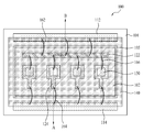
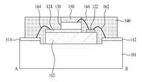
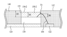
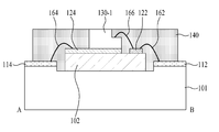
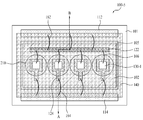
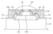
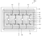
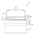
도 1은 실시 예에 따른 램프 유닛(100)의 평면도를 나타내고, 도 2는 도 1에 도시된 램프 유닛(100)의 AB 방향의 단면도를 나타낸다.Fig. 1 shows a plan view of the
도 1 및 도 2를 참조하면, 램프 유닛(100)은 제1 기판(101), 제2 기판(102), 복수의 도전층들(112,114,122,124), 발광 소자(130), 와이어 보호층(140), 파장변환층(150), 및 복수의 와이어들(162,164,166)을 포함한다.1 and 2, the
제2 기판(102)은 제1 기판(101) 상에 배치될 수 있고, 제2 기판(102)의 면적은 제1 기판(101)의 면적보다 작을 수 있다. 다른 실시 예에서는 제2 기판(102)의 면적은 제1 기판(101)의 면적과 동일할 수 있다.The
제1 기판(101)은 제1 열전도율을 갖는 기판일 수 있고, 제2 기판(102)은 제2 열전도율을 갖는 기판일 수 있으며, 제1 열전도율은 제2 열전도율보다 클 수 있다.이는 제2 기판(102) 위에 배치되는 광원(130)으로부터 발생하는 열을 제1 기판(101)을 통하여 외부로 신속하게 방출하기 위함이다.The
제1 기판(101)은 금속 기판, 예컨대, MCPCB(Metal Cored Printed Circuit Board)일 수 있다. 제1 기판(101)은 열전도성이 높은 방열 플레이트로서, 구리(Cu), 알루미늄(Al), 은(Ag), 금(Au)으로부터 선택된 어느 한 물질 또는 그들의 합금으로 형성될 수 있다.The
제2 기판(102)은 절연 기판일 수 있다. 예컨대, 제2 기판(102)은 열전도율이 높은 세라믹 기판일 수 있다. 제2 기판(102)은 질화물, 예컨대, AlN로 형성될 수 있다. 또는 제2 기판(102)은 양극 산화층(anodized layer)을 포함할 수도 있다.The
제1 기판(101)과 제2 기판(102)은 다양한 형태로 형성될 수 있다.The
일 실시 예로서, 제1 기판(101)은 소정 영역에 캐비티(cavity, 105)를 가질 수 있고, 제2 기판(102)은 제 1 기판(101)의 캐비티(105) 내에 배치될 수 있다. 이때 제 1 기판(101)은 Al, Cu, Au 중 적어도 어느 하나를 포함할 수 있고, 제 2 기판(102)은 AlN을 포함할 수 있다.The
다른 실시 예로서, 제1 기판(101)과 제2 기판(102)은 순차적으로 적층된 적층 구조(laminating structure)로 이루어질 수도 있다. 이때, 제1 기판(101)은 Al, Cu, Au 중 적어도 어느 하나를 포함할 수 있고, 제2 기판(102)은 양극 산화층(anodized layer)을 포함할 수 있다.As another example, the
또 다른 실시 예로서, 제1 기판(101)과 제2 기판(102)은 서로 동일한 물질로 이루어질 수 있으며, 이때, 제1 기판(101)과 제2 기판(102)은 AlN, Al, Cu, Au 중 적어도 어느 하나를 포함할 수 있다.The
발광 소자(130)가 배치되는 제2 기판(102)의 상부 표면은 편평한 평면이거나, 오목한 곡면 또는 볼록한 곡면으로 이루어질 수도 있다. 또는 제2 기판(102)의 상부 표면은 오목한 곡면, 볼록한 곡면, 편평한 평면 중 적어도 두 가지의 형상이 혼합된 형태일 수도 있다.The upper surface of the
제3 도전층(112) 및 제4 도전층(114)은 제1 기판(101) 상에 서로 이격하여 배치될 수 있다. 제1 기판(101)은 제3 도전층(112)과 제4 도전층(114)을 포함하는 제1 회로 패턴을 포함할 수 있다. 제3 도전층(112) 및 제4 도전층(114)의 형상은 도 1에 한정되는 것은 아니며, 다양한 형태로 구현될 수 있다.The third
제1 도전층(122) 및 제2 도전층(124)은 제2 기판(102) 상에 서로 이격하여 배치될 수 있다. 제2 기판(102)은 제1 도전층(122)과 제2 도전층(124)을 포함하는 제2 회로 패턴을 포함할 수 있다.The first
발광 소자(130)는 제2 기판(102) 상에 배치된다. 발광 소자(130)의 수는 복수 개일 수 있으며, 복수의 발광 소자들(130)은 서로 이격하여 제2 기판(102) 상에 배치될 수 있다.The
제2 도전층(124)은 복수 개일 수 있으며, 복수의 제2 도전층들은 서로 이격하여 배치될 수 있으나, 이에 한정되는 것은 아니며, 서로 연결된 하나의 도전층을 형성할 수도 있다.A plurality of second
도 1에서 제1 도전층(122)은 한 개이지만, 이에 한정되는 것은 아니며, 복수 개일 수 있으며, 복수의 제1 도전층들은 서로 이격하여 배치될 수 있으며, 각각의 제1 도전층(122)에는 와이어(166)가 본딩될 수 있다.The plurality of first
도 27은 도 1에 도시된 발광 소자(130)의 일 실시 예를 나타낸다.FIG. 27 shows an embodiment of the
도 27을 참조하면, 발광 소자(130)는 제2 전극(405), 보호층(440), 전류 차단층(Current Blocking Layer; 445), 발광 구조물(450), 패시베이션층(465), 및 제1 전극(470)를 포함한다. 예컨대, 발광 소자(130)는 발광 다이오드 칩(light emitting diode chip) 형태일 수 있다.Referring to FIG. 27, the
제2 전극(405)는 제1 전극(470)와 함께 발광 구조물(450)에 전원을 제공한다. 제2 전극(405)는 지지층(support, 410), 접합층(bonding layer, 415), 배리어층(barrier layer, 420), 반사층(reflective layer, 425), 및 오믹층(ohmic layer, 430)을 포함할 수 있다.The
지지층(410)는 발광 구조물(450)을 지지한다. 지지층(410)은 금속 또는 반도체 물질로 형성될 수 있다. 또한 지지층(410)은 전기 전도성과 열 전도성이 높은 물질로 형성될 수 있다. 예컨대, 지지층(410)는 구리(Cu), 구리 합금(Cu alloy), 금(Au), 니켈(Ni), 몰리브덴(Mo), 및 구리-텅스텐(Cu-W) 중 적어도 하나를 포함하는 금속 물질이거나, 또는 Si, Ge, GaAs, ZnO, SiC 중 적어도 하나를 포함하는 반도체일 수 있다.The
접합층(415)은 지지층(410)와 배리어층(420) 사이에 배치될 수 있으며, 지지층(410)과 배리어층(420)을 접합시키는 본딩층(bonding layer)의 역할을 할 수 있다. 접합층(415)은 금속 물질, 예를 들어, In,Sn, Ag, Nb, Pd, Ni, Au, Cu 중 적어도 하나를 포함할 수 있다. 접합층(415)은 지지층(410)을 본딩 방식으로 접합하기 위해 형성하는 것이므로 지지층(410)을 도금이나 증착 방법으로 형성하는 경우에는 접합층(415)은 생략될 수 있다.The
배리어층(420)은 반사층(425), 오믹층(430), 및 보호층(440)의 아래에 배치되며, 접합층(415) 및 지지층(410)의 금속 이온이 반사층(425), 및 오믹층(430)을 통과하여 발광 구조물(450)로 확산하는 것을 방지할 수 있다. 예컨대, 배리어층(420)은 Ni, Pt, Ti,W,V, Fe, Mo 중 적어도 하나를 포함할 수 있으며, 단층 또는 다층으로 이루어질 수 있다.The
반사층(425)은 배리어층(420) 상에 배치될 수 있으며, 발광 구조물(450)로부터 입사되는 광을 반사시켜 주어, 광 추출 효율을 개선할 수 있다. 반사층(425)은 광 반사 물질, 예컨대, Ag, Ni, Al, Rh, Pd, Ir, Ru, Mg, Zn, Pt, Au, Hf 중 적어도 하나를 포함하는 금속 또는 합금으로 형성될 수 있다.The
반사층(425)은 금속 또는 합금과 IZO, IZTO, IAZO, IGZO, IGTO, AZO, ATO 등의 투광성 전도성 물질을 이용하여 다층으로 형성할 수 있으며, 예를 들어, IZO/Ni, AZO/Ag, IZO/Ag/Ni, AZO/Ag/Ni 등으로 형성할 수 있다.The
오믹층(430)은 반사층(425)과 제2 반도체층(452) 사이에 배치될 수 있으며, 제2 반도체층(452)에 오믹 접촉(ohmic contact)되어 발광 구조물(450)에 전원이 원활히 공급되도록 할 수 있다.The
투광성 전도층과 금속을 선택적으로 사용하여 오믹층(430)을 형성할 수 있다. 예컨대 오믹층(430)은 제2 반도체층(452)과 오믹 접촉하는 금속 물질, 예컨대, Ag, Ni,Cr,Ti,Pd,Ir, Sn, Ru, Pt, Au, Hf 중 적어도 어느 하나를 포함할 수 있다.The
보호층(440)은 제2 전극층(405)의 가장 자리 영역 상에 배치될 수 있다. 예컨대, 보호층(440)은 오믹층(430)의 가장 자리 영역, 또는 반사층(425)의 가장 자리 영역, 또는 배리어층(420)의 가장 자리 영역, 또는 지지층(410)의 가장 자리 영역 상에 배치될 수 있다.The
보호층(440)은 발광 구조물(450)과 제2 전극층(405) 사이의 계면이 박리되어 발광 소자(130)의 신뢰성이 저하되는 것을 방지할 수 있다. 보호층(440)은 전기 절연성 물질, 예를 들어, ZnO, SiO2, Si3N4, TiOx(x는 양의 실수), 또는 Al2O3 등으로 형성될 수 있다.The
전류 차단층(445)은 오믹층(430)과 발광 구조물(450) 사이에 배치될 수 있다. 전류 차단층(445)의 상면은 제2 반도체층(452)과 접촉하고, 전류 차단층(445)의 하면, 또는 하면과 측면은 오믹층(430)과 접촉할 수 있다. 전류 차단층(445)은 수직 방향으로 제1 전극(470)와 적어도 일부가 공간적으로 오버랩되도록 배치될 수 있다.The
전류 차단층(445)은 오믹층(430)과 제2 반도체층(452) 사이에 형성되거나, 반사층(425)과 오믹층(430) 사이에 형성될 수 있으며, 이에 대해 한정하지는 않는다.The
발광 구조물(450)은 오믹층(430) 및 보호층(440) 상에 배치될 수 있다. 발광 구조물(450)의 측면은 단위 칩으로 구분하는 아이솔레이션(isolation) 에칭 과정에서 경사면이 될 수 있다. 발광 구조물(450)은 제2 반도체층(452), 활성층(454), 및 제1 반도체층(456)을 포함할 수 있으며, 빛을 발생할 수 있다.The
제2 반도체층(452)은 3족-5족, 2족-6족 등의 화합물 반도체로 구현될 수 있으며, 제2 도전형 도펀트가 도핑될 수 있다. 예컨대, 제2 반도체층(452)은 InxAlyGa1-x-yN(0≤x≤1, 0≤y≤1, 0≤x+y≤1)의 조성식을 갖는 반도체일 수 있으며, p형 도펀트(예컨대, Mg, Zn, Ca, Sr, Ba)가 도핑될 수 있다.The
활성층(454)은 제1 반도체층(456) 및 제2 반도체층(452)으로부터 제공되는 전자(electron)와 정공(hole)의 재결합(recombination) 과정에서 발생하는 에너지에 의해 광을 생성할 수 있다.The
활성층(454)은 반도체 화합물, 예컨대, 3족-5족, 2족-6족의 화합물 반도체일 수 있으며, 단일 우물 구조, 다중 우물 구조, 양자 선(Quantum-Wire) 구조, 또는 양자 점(Quantum Dot) 구조 등으로 형성될 수 있다. 활성층(454)이 양자우물구조인 경우에는 InxAlyGa1 -x- yN (0≤x≤1, 0≤y≤1, 0≤x+y≤1)의 조성식을 갖는 우물층과 InaAlbGa1-a-bN (0≤a≤1, 0≤b≤1, 0≤a+b≤1)의 조성식을 갖는 장벽층을 갖는 단일 또는 양자우물구조를 가질 수 있다. 우물층은 장벽층의 에너지 밴드 갭보다 낮은 밴드 갭을 갖는 물질일 수 있다.The
제1 반도체층(456)은 3족-5족, 2족-6족 등의 화합물 반도체로 구현될 수 있으며, 제1 도전형 도펀트가 도핑될 수 있다. 예컨대, 제1 반도체층(456)은 InxAlyGa1-x-yN (0≤x≤1, 0≤y≤1, 0≤x+y≤1)의 조성식을 가지는 반도체일 수 있으며, n형 도펀트(예: Si, Ge, Sn, Se, Te 등)가 도핑될 수 있다.The
발광 구조물(450)의 조성에 따라 발광 소자(130)는 제1 반도체층(456), 활성층(454), 및 제2 반도체층(452)의 조성에 따라 청색광, 적색광, 녹색광, 또는 황색광 중 어느 하나를 방출할 수 있다.Depending on the composition of the
패시베이션층(465)은 발광 구조물(450)을 전기적으로 보호하기 위하여 발광 구조물(450)의 측면에 배치될 수 있다. 패시베이션층(465)은 제1 반도체층(456)의 상면 일부 또는 보호층(440)의 상면에도 배치될 수 있다. 패시베이션층(465)은 절연 물질, 예컨대, SiO2, SiOx, SiOxNy, Si3N4, 또는 Al2O3 로 형성될 수 있다.The
제1 전극(470)는 제1 반도체층(456) 상에 배치될 수 있다. 제1 전극(470)은 소정의 패턴 형상일 수 있다. 제1 전극(470)은 와이어 본딩을 위한 패드부, 및 패드부로부터 확장되는 가지 전극(미도시)을 포함할 수 있다.The
제1 반도체층(456)의 상면은 광 추출 효율을 증가시키기 위해 러프니스 패턴(미도시)이 형성될 수 있다. 또한 광 추출 효율을 증가시키기 위하여 제1 전극(470)의 상면에도 러프니스 패턴(미도시)이 형성될 수 있다.A roughness pattern (not shown) may be formed on the upper surface of the
발광 소자(130)는 제1 도전층(122)과 제2 도전층(124)에 전기적으로 연결될 수 있다.The
유테틱 본딩(eutectic bonding) 또는 다이 본딩(die bonding)을 이용하여 발광 소자(130)의 제2 전극(405)은 제2 기판(102) 상에 배치된 제2 도전층(124)에 본딩되어 제2 도전층(124)과 전기적으로 연결될 수 있다.The
와이어(166)는 발광 소자(130)의 제1 전극(470)과 제2 기판(102) 상에 배치된 제1 도전층(122)을 전기적으로 연결할 수 있다.The
와이어(162)는 제2 기판(102) 상에 배치된 제1 도전층(122)과 제1 기판(101) 상에 배치된 제3 도전층(112)을 전기적으로 연결할 수 있다. 와이어(162)의 수는 1개 이상일 수 있다.The
와이어(164)는 제2 기판(102) 상에 배치된 제2 도전층(124)과 제1 기판(101) 상에 마련된 제4 도전층(114)을 전기적으로 연결할 수 있다. 와이어(164)의 수는 1개 이상일 수 있다.The
파장 변환층(150)은 발광 소자(130)의 상부에 위치하며, 발광 소자(130)로부터 발생하는 빛의 파장을 변화시킬 수 있다. 파장 변환층(150)은 에폭시 또는 실리콘과 같은 무색 투명한 고분자 수지 및 형광체를 포함할 수 있다. 파장 변화층(150)은 적색 형광체, 녹색 형광체, 및 황색 형광체 중 적어도 하나를 포함할 수 있다. 파장 변환층(150)은 와이어(166)의 일부를 감쌀 수 있다.The
와이어 보호층(140)은 발광 소자(130), 및 와이어들(162 내지 166)을 포위하도록 제1 기판(101), 및 제2 기판(102) 상에 배치된다. 와이어 보호층(140)은 제1 기판(101)의 캐비티(105)를 채울 수 있다. 와이어 보호층(140)의 상부면은 와이어(166)의 최고점보다 높게 위치할 수 있다.The
와이어 보호층(140)은 와이어들(162 내지 166)을 포위하고, 와이어들(162 내지 166)이 외부로 노출되거나, 돌출되는 것을 방지할 수 있다. 와이어 보호층을 구비함으로써, 실시 예는 와이어(예컨대, 166)가 충격 또는 압력에 의하여 파손 또는 변형되거나, 공기 등에 의하여 부식되는 것을 방지할 수 있고, 이로 인하여 발광 소자(100)의 파손 또는 오동작을 방지할 수 있다.The
와이어 보호층(140)은 빛을 반사할 수 있는 비전도성 몰딩(molding) 부재, 예컨대, 화이트 실리콘(white silicon)로 이루어질 수 있으나, 이에 한정되는 것은 아니다. The
와이어 보호층(140)은 발광 소자들(130)과 밀착하며, 발광 소자들(130)로부터 조사되는 빛을 바로 반사시키기 때문에 실시 예는 공기 또는 제1 기판(101) 및 제2 기판(102)에 의한 흡수 및 투과에 의한 광 손실을 감소시킬 수 있으며, 발광 효율을 향상시킬 수 있다.The
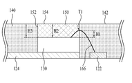
도 3은 제1 실시 예에 따른 파장 변환층(150)과 와이어(166)의 확대도이다.3 is an enlarged view of the
도 3을 참조하면, 와이어 보호층(140)은 파장 변환층(150)의 측면(152) 및 발광 소자(130)의 측면과 접할 수 있고, 파장 변환층(150)의 측면(152)을 감쌀 수 있다.3, the
파장 변환층(150)의 상부면(154)은 편평할 수 있으며, 와이어 보호층(140)으로부터 노출될 수 있다.The
파장 변환층(150)의 상부면(154)은 와이어 보호층(140)의 상부면(142)과 동일 평면 상에 위치할 수 있다. 발광 소자(130)의 상면으로부터 파장 변화층(150)의 상부면(154)까지의 높이(H2)는 발광 소자(130)의 상면으로부터 와이어 보호층(140)의 상부면(142)까지의 높이(H3)와 동일할 수 있다(H2=H3).The
와이어(166)를 보호하기 위하여, 파장 변환층(150)의 상부면(154) 및 와이어 보호층(140)의 상부면(142)은 와이어(166)의 최고점(T1)보다 높게 위치할 수 있다.The
발광 소자(130)의 상면으로부터 파장 변환층(150)의 상부면(154) 및 와이어 보호층(140)의 상부면(142)까지의 높이는 적어도 50㎛를 초과할 수 있다. 실질적으로 공정상 가능한 와이어(166)의 최고점(T1)의 최저 높이(H1)가 50㎛ 정도이기 때문이다. 따라서 발광 소자(130)의 상면으로부터 파장 변환층(150)의 상부면(154) 및 와이어 보호층(140)의 상부면(142)까지의 높이가 50㎛ 이하일 경우 와이어(166)가 와이어 보호층(140)으로부터 노출될 수 있다.The height from the upper surface of the
발광 소자(130)의 상면으로부터 파장 변환층(150)의 상부면(154)까지의 높이(H2)는 발광 소자(130)의 상면으로부터 와이어(166)의 최고점(T1)까지의 높이(H1)보다 높을 수 있다(H2>H1). 이는 와이어(166)의 노출을 방지하기 위함이다.The height H2 from the upper surface of the
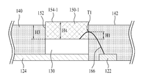
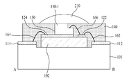
도 4는 제2 실시 예에 따른 파장 변환층(150-1)과 와이어(166)의 확대도이다.4 is an enlarged view of the wavelength conversion layer 150-1 and the
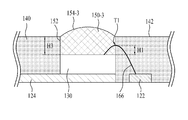
도 4를 참조하면, 파장 변환층(150-1)의 상부면(154-1)은 와이어 보호층(140)의 상부면(142)보다 높게 위치할 수 있다. 파장 변환층(150-1)의 상부면(154-1)은 와이어 보호층(140)의 상부면(142)으로부터 돌출된 구조일 수 있다.Referring to FIG. 4, the upper surface 154-1 of the wavelength conversion layer 150-1 may be positioned higher than the
발광 소자(130)의 상면으로부터 파장 변화층(150-1)의 상부면(154-1)까지의 높이(H4)는 발광 소자(130)의 상면으로부터 와이어 보호층(140)의 상부면(142)까지의 높이(H3)보다 높을 수 있다(H4>H3).The height H4 from the upper surface of the
도 5는 제3 실시 예에 따른 파장 변환층(150-2)과 와이어(166)의 확대도이다.5 is an enlarged view of the wavelength conversion layer 150-2 and the
도 5를 참조하면, 파장 변환층(150-2)의 상부면(154-2)은 와이어 보호층(140)의 상부면(142)보다 낮게 위치할 수 있다. 발광 소자(130)의 상면으로부터 파장 변화층(150-2)의 상부면(154-2)까지의 높이(H5)는 발광 소자(130)의 상면으로부터 와이어 보호층(140)의 상부면(142)까지의 높이(H3)보다 낮고, 와이어(166)의 최고점(T1)의 높이(H1)보다 높을 수 있다(H1<H5<H3).Referring to FIG. 5, the upper surface 154-2 of the wavelength conversion layer 150-2 may be positioned lower than the
도 6은 제4 실시 예에 따른 파장 변환층(150-3)과 와이어(166)의 확대도이다.6 is an enlarged view of the wavelength conversion layer 150-3 and the
도 6을 참조하면, 파장 변화층(150-3)의 상부면(154-3)은 곡면일 수 있다. 파장 변환층(150-3)의 상부면(154-3)이 곡면이기 때문에, 제4 실시 예는 발광 소자(130)로부터 조사되는 빛을 굴절시켜 지향각을 향상시킬 수 있다.Referring to FIG. 6, the upper surface 154-3 of the wavelength variable layer 150-3 may be a curved surface. Since the upper surface 154-3 of the wavelength conversion layer 150-3 is a curved surface, the fourth embodiment can refract light emitted from the
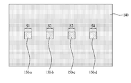
도 7은 일 실시 예에 따른 파장 변환층(150)을 나타낸다.7 shows a
도 7을 참조하면, 파장 변환층(150)은 발광 소자들(130) 각각이 위치하는 영역들(S1 내지 S4)에 대응하도록 위치할 수 있다. 파장 변환층(150)은 복수 개의 서로 이격하는 부분들(예컨대, 150-a, 150-b,150-c,150-d)을 포함할 수 있으며, 부분들(예컨대, 150-a, 150-b,150-c,150-d) 각각은 발광 소자들 중 어느 하나와 대응하도록 위치할 수 있다.Referring to FIG. 7, the
도 8은 다른 실시 예에 따른 파장 변환층(150')을 나타낸다.8 shows a wavelength conversion layer 150 'according to another embodiment.
도 8을 참조하면, 파장 변환층(150')은 발광 소자들 각각이 위치하는 영역 및 인접하는 2개의 발광 소자들 사이의 영역을 모두 합한 영역(S5)과 대응하도록 위치할 수 있으며, 하나의 부분으로 이루어질 수 있다.Referring to FIG. 8, the wavelength conversion layer 150 'may be positioned so as to correspond to a region S5 in which the light emitting elements are located and the region between two adjacent light emitting elements, ≪ / RTI >
도 9는 다른 실시 예에 따른 램프 유닛(100-1)의 단면도를 나타낸다. 도 2와 동일한 도면 부호는 동일한 구성을 나타내며, 동일한 구성에 대해서는 중복을 피하기 위하여 설명을 간략히 하거나, 생략한다.Fig. 9 shows a cross-sectional view of a lamp unit 100-1 according to another embodiment. The same reference numerals as those in FIG. 2 denote the same components, and the description of the same components will be simplified or omitted in order to avoid redundancy.
도 9를 참조하면, 램프 유닛(100-1)이 도 2에 도시된 실시 예(100)와 다른 점은 와이어 보호층(140-1)이 투광성이라는 점이다.Referring to Fig. 9, the lamp unit 100-1 is different from the
즉 와이어 보호층(140-1)은 빛을 투과할 수 있는 비전도성 몰딩 부재로 이루어질 수 있다. 예컨대, 와이어 보호층(140-1)은 실리콘 수지, 에폭시 수지, 글래스(glass), 글래스 세라믹(glass ceramic), 폴리에스테르 수지, 아크릴 수지, 우레탄 수지, 나일론 수지, 폴리아미드 수지, 폴리이미드 수지, 염화비닐 수지, 폴리카보네이트 수지, 폴리에틸렌 수지, 테프론 수지, 폴리스틸렌 수지, 폴리프로필렌 수지, 폴리올레핀 수지 등으로 이루어질 수 있다.That is, the wire protection layer 140-1 may be made of a nonconductive molding member capable of transmitting light. For example, the wire protecting layer 140-1 may be formed of a resin such as a silicone resin, an epoxy resin, a glass, a glass ceramic, a polyester resin, an acrylic resin, a urethane resin, a nylon resin, a polyamide resin, A polyvinyl chloride resin, a polycarbonate resin, a polyethylene resin, a Teflon resin, a polystyrene resin, a polypropylene resin, a polyolefin resin and the like.
도 9에 도시된 와이어 보호층(140-1)은 상술한 와이어 보호층(140)과 재질만 다를 뿐이고, 나머지는 상술한 바와 동일할 수 있다.The wire protection layer 140-1 shown in FIG. 9 is different from the
도 10은 다른 실시 예에 따른 램프 유닛(100-2)의 평면도를 나타내고, 도 11은 도 10에 도시된 램프 유닛(100-2)의 AB 방향의 단면도를 나타낸다. 도 2와 동일한 도면 부호는 동일한 구성을 나타내며, 동일한 구성에 대해서는 중복을 피하기 위하여 설명을 간략히 하거나, 생략한다.Fig. 10 shows a plan view of the lamp unit 100-2 according to another embodiment, and Fig. 11 shows a sectional view in the AB direction of the lamp unit 100-2 shown in Fig. The same reference numerals as those in FIG. 2 denote the same components, and the description of the same components will be simplified or omitted in order to avoid redundancy.
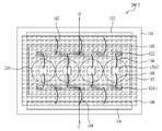
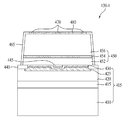
도 10 및 도 11을 참조하면, 램프 유닛(100-2)은 도 2에 도시된 실시 예(100)에 렌즈(210)를 더 포함한다.Referring to FIGS. 10 and 11, the lamp unit 100-2 further includes a
렌즈(210)는 발광 소자들(130) 각각에 대응하도록 파장 변환층(150) 및 와이어 보호층(140) 상에 배치될 수 있다. 렌즈(210)는 대응하는 발광 소자로부터 조사되는 빛을 굴절시킬 수 있으며, 램프 유닛(100-2)의 광 경로를 조절할 수 있다.The
도 10에서는 각 발광 소자에 대응하는 렌즈(210)를 도시하였지만, 다른 실시 예에서는 발광 소자들 전체를 덮는 하나의 렌즈로 구현할 수 있다.Although the
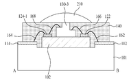
도 12는 다른 실시 예에 따른 램프 유닛(100-3)의 평면도를 나타내고, 도 13은 도 12에 도시된 램프 유닛(100-3)의 AB 방향의 단면도를 나타낸다. 도 2와 동일한 도면 부호는 동일한 구성을 나타내며, 동일한 구성에 대해서는 중복을 피하기 위하여 설명을 간략히 하거나, 생략한다.Fig. 12 shows a plan view of the lamp unit 100-3 according to another embodiment, and Fig. 13 shows a sectional view in the AB direction of the lamp unit 100-3 shown in Fig. The same reference numerals as those in FIG. 2 denote the same components, and the description of the same components will be simplified or omitted in order to avoid redundancy.
도 12 및 도 13을 참조하면, 램프 유닛(100-3)은 제1 기판(101), 제2 기판(102), 복수의 도전층들(112,114,122,124), 발광 소자(130-1), 와이어 보호층(140), 및 복수의 와이어들(162,164,166)을 포함한다.12 and 13, the lamp unit 100-3 includes a
도 12 및 도 13을 참조하면, 도 2에 도시된 실시 예는 칩 형태의 발광 소자(130)와 발광 소자(130) 상에 위치하는 파장 변환층(150)을 구비하지만, 램프 유닛(100-3)은 도 2에 도시된 실시 예(100)의 발광 소자(130)와 파장 변환층(150)이 하나의 칩으로 구현된 발광 소자(130-1)를 포함한다.2 and FIG. 13, the embodiment shown in FIG. 2 includes the chip-type
예컨대, 발광 소자(130)는 청색광, 녹색광, 적색광, 또는 황색광 중 어느 하나를 방출할 수 있으며, 발광 소자(130-1)는 백색광을 방출할 수 있다.For example, the
도 28은 도 13에 도시된 발광 소자(130-1)의 일 실시 예를 나타낸다. 도 27과 동일한 도면 부호는 동일한 구성을 나타내며, 동일한 구성에 대해서는 중복을 피하기 위하여 설명을 간략히 하거나, 생략한다.Fig. 28 shows an embodiment of the light emitting device 130-1 shown in Fig. The same reference numerals as those in FIG. 27 denote the same components, and a description of the same components will be simplified or omitted in order to avoid redundancy.
도 28을 참조하면, 발광 소자(130-1)는 파장 변환층(480)을 더 포함한다.Referring to FIG. 28, the light emitting device 130-1 further includes a
파장 변환층(480)은 제1 반도체층(456) 상에 배치될 수 있으며, 제1 전극(470)을 노출할 수 있다.The
예컨대, 파장 변환층(480)은 에폭시 또는 실리콘과 같은 무색 투명한 고분자 수지와 형광체의 혼합물일 수 있으며, 고분자 수지와 형광체의 혼합물을 제1 반도체층(456) 상에 컨포멀 코팅(conformal coating)하여 파장 변환층(480)을 형성할 수 있다. 파장 변환층(480)은 와이어 본딩을 위하여 제1 전극(470)의 패드부(미도시)를 노출할 수 있다.For example, the
와이어 보호층(140)의 상부면은 제2 기판(102) 상에 배치되는 도전층(122)에 본딩되는 와이어(166)의 최고점보다 높게 위치할 수 있다. 와이어 보호층(140)은 와이어들(162 내지 166)을 포위하고, 와이어들(162 내지 166)이 외부로 노출되거나, 돌출되는 것을 방지할 수 있다.The upper surface of the
와이어 보호층(140)은 발광 소자(130-1)의 측면과 접할 수 있으며, 발광 소자(130-1)의 상면은 와이어 보호층(140)으로부터 노출될 수 있다.The
와이어 보호층(140)의 상부면은 발광 소자(130-1)의 상부면과 동일 평면 상에 위치할 수 있다. 즉 발광 소자(130)의 상면의 높이는 와이어 보호층(140)의 상부면의 높이와 동일할 수 있다. 이때 발광 소자(130)의 상면은 파장 변환층(480)의 상부면일 수 있다.The top surface of the
도 14는 다른 실시 예에 따른 램프 유닛(100-4)의 단면도를 나타낸다. 도 13과 동일한 도면 부호는 동일한 구성을 나타내며, 동일한 구성에 대해서는 중복을 피하기 위하여 설명을 간략히 하거나, 생략한다.Fig. 14 shows a cross-sectional view of a lamp unit 100-4 according to another embodiment. The same reference numerals as those in FIG. 13 denote the same components, and a description of the same components will be simplified or omitted in order to avoid redundancy.
도 14를 참조하면, 램프 유닛(100-4)이 도 13에 도시된 실시 예(100-3)와 다른 점은 와이어 보호층(140-1)이 투광성 몰딩 부재이라는 점이다. 도 14에 도시된 와이어 보호층(140-1)은 상술한 와이어 보호층(140)과 재질만 다를 뿐이고, 나머지는 상술한 바와 동일할 수 있다.Referring to Fig. 14, the lamp unit 100-4 is different from the embodiment 100-3 shown in Fig. 13 in that the wire protecting layer 140-1 is a light-transmitting molding member. The wire protection layer 140-1 shown in FIG. 14 is different from the above-described
도 15는 다른 실시 예에 따른 램프 유닛(100-5)의 평면도를 나타내고, 도 16은 도 15에 도시된 램프 유닛(100-5)의 AB 방향의 단면도를 나타낸다.Fig. 15 shows a plan view of the lamp unit 100-5 according to another embodiment, and Fig. 16 shows a sectional view in the AB direction of the lamp unit 100-5 shown in Fig.
도 15 및 도 16을 참조하면, 램프 유닛(100-5)은 도 13에 도시된 실시 예(100-3)에 렌즈(210)를 더 포함한다.Referring to Figs. 15 and 16, the lamp unit 100-5 further includes a
렌즈(210)는 발광 소자들(130-1) 각각에 대응하도록 와이어 보호층(140) 상에 배치될 수 있다. 렌즈(210)는 대응하는 발광 소자로부터 조사되는 빛을 굴절시킬 수 있으며, 램프 유닛(100-5)의 광 경로를 조절할 수 있다.The
도 12에서는 각 발광 소자에 대응하는 렌즈(210)를 도시하였지만, 다른 실시 예에서는 발광 소자들 전체를 덮는 하나의 렌즈로 구현할 수 있다.Although the
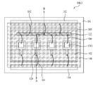
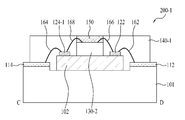
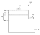
도 17은 다른 실시 예에 따른 램프 유닛(200)의 평면도를 나타내고, 도 18은 도 17에 도시된 램프 유닛(200)의 CD 방향의 단면도를 나타낸다. 도 1 및 도 2와 동일한 도면 부호는 동일한 구성을 나타내고, 동일한 구성에 대해서는 중복을 피하기 위하여 설명을 간략히 하거나, 생략한다.Fig. 17 shows a plan view of the
도 17 및 도 18을 참조하면, 램프 유닛(200)은 제1 기판(101), 제2 기판(102), 복수의 도전층들(112,114,122,124-1), 발광 소자(130-2), 와이어 보호층(140), 파장변환층(150), 및 복수의 와이어들(162,164,166, 168)을 포함한다.17 and 18, the
도 2에 도시된 램프 유닛(100)과 다른 점은 발광 소자(130-2)가 수평형 발광 다이오드라는 것과, 이에 따른 도전층들(112,114,122,124-1)과의 전기적 연결 구조이다.The
발광 소자(130-2)는 제2 기판(102) 상에 배치될 수 있다.The light emitting device 130-2 may be disposed on the
도 29는 도 18에 도시된 발광 소자(130-2)의 일 실시 예를 나타낸다.FIG. 29 shows an embodiment of the light emitting device 130-2 shown in FIG.
도 29를 참조하면, 발광 소자(130-2)는 기판(310), 발광 구조물(320), 전도층(330), 제1 전극(342), 및 제2 전극(344)을 포함한다.Referring to FIG. 29, the light emitting device 130-2 includes a
기판(310)은 반도체 물질 성장에 적합한 물질, 캐리어 웨이퍼로 형성될 수 있다. 또한 기판(310)은 열전도성이 뛰어난 물질로 형성될 수 있으며, 전도성 기판 또는 절연성 기판일 수 있다. 예를 들어 기판(310)은 사파이어(Al203), GaN, SiC, ZnO, Si, GaP, InP, Ga203, GaAs 중 적어도 하나를 포함하는 물질일 수 있다. 이러한 기판(310)의 상면에는 요철 패턴이 형성될 수 있다.The
또한 기판(310) 위에는 2족 내지 6족 원소의 화합물 반도체를 이용한 층 또는 패턴, 예컨대, ZnO층(미도시), 버퍼층(미도시), 언도프드 반도체층(미도시) 중 적어도 한 층이 형성될 수 있다. 버퍼층 또는 언도프드 반도체층은 3족-5족 원소의 화합물 반도체를 이용하여 형성될 수 있으며, 버퍼층은 기판과의 격자 상수의 차이를 줄여주게 되며, 언도프드 반도체층은 도핑하지 않는 GaN계 반도체로 형성될 수 있다.On the
발광 구조물(450)은 빛을 발생하는 반도체층일 수 있으며, 제1 반도체층(456), 활성층(454), 및 제2 반도체층(452)을 포함할 수 있다. 제1 반도체층(456), 활성층(454), 및 제2 반도체층(452)은 도 27에서 설명한 바와 동일할 수 있다. 발광 소자(130-2)는 청색광, 녹색광, 적색광, 또는 황색광 중 어느 하나를 방출할 수 있다.The
발광 구조물(450)은 제2 반도체층(452), 활성층(454) 및 제1 반도체층(456)의 일부가 제거되어 제1 반도체층(456)의 일부를 노출할 수 있다.The
전도층(330)은 전반사를 감소시킬 뿐만 아니라, 투광성이 좋기 때문에 활성층(454)으로부터 제2 반도체층(452)으로 방출되는 빛의 추출 효율을 증가시킬 수 있다.The
전도층(330)은 투명 전도성 산화물, 예컨대, ITO(Indium Tin Oxide), TO(Tin Oxide), IZO(Indium Zinc Oxide), ITZO(Indium Tin Zinc Oxide), IAZO(Indium Aluminum Zinc Oxide), IGZO(Indium Gallium Zinc Oxide), IGTO(Indium Gallium Tin Oxide), AZO(Aluminum Zinc Oxide), ATO(Antimony tin Oxide), GZO(Gallium Zinc Oxide), IrOx, RuOx,RuOx/ITO, Ni, Ag, Ni/IrOx/Au, 또는 Ni/IrOx/Au/ITO 중 하나 이상을 이용하여 단층 또는 다층으로 이루어질 수 있다.The
제1 전극(342)은 노출되는 제1 반도체층(456) 상에 배치될 수 있고, 제2 전극(344)은 전도층(330) 상에 배치될 수 있다.The
제1 도전층(122)과 제4 도전층(124-1)은 제2 기판(102) 상에 서로 이격하여 위치하고, 발광 소자(130-2)는 제1 도전층(122)과 제4 도전층(124-1)에 전기적으로 연결될 수 있다.The first
발광 소자(130-2)의 기판(310)은 제2 기판(102)에 본딩될 수 있다.The
와이어(166)는 발광 소자(130-2)의 제1 전극(342)과 제2 기판(102) 상에 배치된 제1 도전층(122)을 전기적으로 연결할 수 있다. 와이어(168)는 발광 소자(130-2)의 제2 전극(344)과 제2 기판(102) 상에 배치된 제4 도전층(124-1)을 전기적으로 연결할 수 있다.The
와이어들(166, 168)를 보호하기 위하여, 파장 변환층(150)의 상부면 및 와이어 보호층(140)의 상부면은 와이어들(166, 168) 각각의 최고점(T1)보다 높게 위치할 수 있다.The upper surface of the
도 19는 다른 실시 예에 따른 램프 유닛(200-1)을 나타낸다. 도 18과 동일한 도면 부호는 동일한 구성을 나타내고, 동일한 구성에 대해서는 중복을 피하기 위하여 설명을 간략히 하거나, 생략한다.Fig. 19 shows a lamp unit 200-1 according to another embodiment. The same reference numerals as those in FIG. 18 denote the same components, and a description of the same components will be simplified or omitted in order to avoid redundancy.
도 19를 참조하면, 램프 유닛(200-1)이 도 18에 도시된 실시 예(200)와 다른 점은 와이어 보호층(140-1)이 투광성이라는 점이다.Referring to FIG. 19, the lamp unit 200-1 is different from the
도 20은 다른 실시 예에 따른 램프 유닛(200-2)의 평면도를 나타내고, 도 21은 도 20에 도시된 램프 유닛(200-2)의 CD 방향의 단면도를 나타낸다. 도 18과 동일한 도면 부호는 동일한 구성을 나타내고, 동일한 구성에 대해서는 중복을 피하기 위하여 설명을 간략히 하거나, 생략한다.Fig. 20 shows a plan view of the lamp unit 200-2 according to another embodiment, and Fig. 21 shows a sectional view in the CD direction of the lamp unit 200-2 shown in Fig. The same reference numerals as those in FIG. 18 denote the same components, and a description of the same components will be simplified or omitted in order to avoid redundancy.
도 20 및 도 21을 참조하면, 램프 유닛(200-2)은 도 18에 도시된 실시 예(200)에 렌즈(210)를 더 포함한다. 렌즈(210)는 발광 소자들(130-2) 각각에 대응하도록 파장 변환층(150) 및 와이어 보호층(140) 상에 배치될 수 있다. 렌즈(210)는 대응하는 발광 소자(130-2)로부터 조사되는 빛을 굴절시킬 수 있으며, 램프 유닛(200-2)의 광 경로를 조절할 수 있다.Referring to FIGS. 20 and 21, the lamp unit 200-2 further includes a
도 22는 다른 실시 예에 따른 램프 유닛(200-3)의 평면도를 나타내고, 도 23은 도 22에 도시된 램프 유닛(200-3)의 CD 방향의 단면도를 나타낸다. 도 17 및 도 18과 동일한 도면 부호는 동일한 구성을 나타내고, 동일한 구성에 대해서는 중복을 피하기 위하여 설명을 간략히 하거나, 생략한다.Fig. 22 shows a plan view of the lamp unit 200-3 according to another embodiment, and Fig. 23 shows a sectional view in the CD direction of the lamp unit 200-3 shown in Fig. The same reference numerals as in Figs. 17 and 18 denote the same components, and a description of the same components will be simplified or omitted in order to avoid redundancy.
도 22 및 도 23을 참조하면, 램프 유닛(200-3)은 제1 기판(101), 제2 기판(102), 복수의 도전층들(112,114,122,124-1), 발광 소자(130-3), 와이어 보호층(140), 및 복수의 와이어들(162,164,166,168)을 포함한다.22 and 23, the lamp unit 200-3 includes a
도 22 및 도 23을 참조하면, 도 18에 도시된 실시 예는 칩 형태의 발광 소자(130-2)와 발광 소자(130-2) 상에 위치하는 파장 변환층(150)을 구비하지만, 램프 유닛(200-3)은 도 18에 도시된 실시 예(200)의 발광 소자(130-2)와 파장 변환층(150)이 하나의 칩으로 구현된 발광 소자(130-3)를 포함한다.22 and 23, the embodiment shown in FIG. 18 includes the chip-type light emitting device 130-2 and the
예컨대, 발광 소자(130-2)는 청색광, 녹색광, 적색광, 또는 황색광 중 어느 하나를 방출할 수 있으며, 발광 소자(130-3)는 백색광을 방출할 수 있다.For example, the light emitting device 130-2 may emit one of blue light, green light, red light, or yellow light, and the light emitting device 130-3 may emit white light.
도 30은 도 23에 도시된 발광 소자(130-3)의 일 실시 예를 나타낸다. 도 29와 동일한 도면 부호는 동일한 구성을 나타내며, 동일한 구성에 대해서는 중복을 피하기 위하여 설명을 간략히 하거나, 생략한다.Fig. 30 shows an embodiment of the light emitting device 130-3 shown in Fig. The same reference numerals as those in FIG. 29 denote the same components, and a description of the same components will be simplified or omitted in order to avoid redundancy.
도 30을 참조하면, 발광 소자(130-3)는 파장 변환층(350)을 더 포함한다.Referring to FIG. 30, the light emitting device 130-3 further includes a
파장 변환층(350)은 제2 반도체층(452) 상에 배치될 수 있으며, 제1 전극(344)을 노출할 수 있다.The
와이어 보호층(140)의 상부면은 발광 소자(130-3)의 상면과 동일 평면 상에 위치할 수 있다. 발광 소자(130)의 상면의 높이는 와이어 보호층(140)의 상부면의 높이와 동일할 수 있다. 이때 발광 소자(130-3)의 상면은 파장 변환층(350)의 상부면일 수 있다.The upper surface of the
와이어 보호층(140)은 발광 소자(130-3)의 측면과 접할 수 있으며, 발광 소자(130-3)의 상면은 와이어 보호층(140)으로부터 노출될 수 있다.The
와이어들(166, 168)의 최고점의 높이는 발광 소자(130-3)의 상면의 높이 및 와이어 보호층(140)의 상부면의 높이보다 낮기 때문에, 실시 예는 와이어들(166, 168)의 파손 및 변형을 방지할 수 있다.Since the height of the highest point of the
도 24는 다른 실시 예에 따른 램프 유닛(200-4)의 단면도를 나타낸다. 도 23과 동일한 도면 부호는 동일한 구성을 나타내며, 동일한 구성에 대해서는 중복을 피하기 위하여 설명을 간략히 하거나, 생략한다.24 shows a cross-sectional view of a lamp unit 200-4 according to another embodiment. The same reference numerals as those in FIG. 23 denote the same components, and the description of the same components will be simplified or omitted in order to avoid redundancy.
도 24를 참조하면, 도 23에 도시된 램프 유닛(200-3)의 와이어 보호층(140)은 반사 부재인데 반하여, 램프 유닛(200-4)의 와이어 보호층(140-1)은 투광성일 수 있다.24, the wire protection layer 140-1 of the lamp unit 200-3 is a reflective member, while the wire protection layer 140-1 of the lamp unit 200-3 is a reflective member, .
도 25는 다른 실시 예에 따른 램프 유닛(200-5)의 평면도를 나타내고, 도 26은 도 25에 도시된 램프 유닛(200-5)의 CD 방향의 단면도를 나타낸다.Fig. 25 shows a plan view of the lamp unit 200-5 according to another embodiment, and Fig. 26 shows a sectional view in the CD direction of the lamp unit 200-5 shown in Fig.
도 22 및 도 23과 동일한 도면 부호는 동일한 구성을 나타내며, 동일한 구성에 대해서는 중복을 피하기 위하여 설명을 간략히 하거나, 생략한다.The same reference numerals as in Figs. 22 and 23 denote the same constituent elements, and a description of the same constituent elements will be simplified or omitted in order to avoid redundancy.
도 25 및 도 26을 참조하면, 발광 소자(130-3)로부터 조사되는 빛을 굴절시키고, 광 경로를 조절하기 위하여, 램프 유닛(200-5)은 도 23에 도시된 실시 예(200-3)에 렌즈(210)를 더 포함할 수 있다.Referring to FIGS. 25 and 26, in order to refract light emitted from the light emitting device 130-3 and adjust the optical path, the lamp unit 200-5 is similar to the embodiment 200-3 (Not shown).
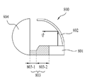
도 31은 실시 예에 따른 차량용 헤드 램프(800)의 단면도를 나타낸다.Fig. 31 shows a sectional view of a
도 31을 참조하면, 헤드 램프(800)는 램프 유닛(801), 리플렉터(reflector)(802), 쉐이드(803), 및 렌즈(804)를 포함한다.31, the
램프 유닛(801)은 실시 예들(100, 100-1 내지 100-5, 200, 200-1 내지 200-5) 중 어느 하나일 수 있으며, 빛을 발생할 수 있다.The
리플렉터(802)는 램프 유닛(801)로부터 조사되는 광을 일정 방향으로 반사시킬 수 있다. 쉐이드(803)는 리플렉터(802)와 렌즈(804) 사이에 배치될 수 있고, 리플렉터(802)에 의하여 반사되어 렌즈(804)로 향하는 광의 일부분을 차단 또는 반사하여 설계자가 원하는 배광 패턴을 이루도록 하는 부재이다.The
여기서, 렌즈(804)에 인접하는 쉐이드(803)의 일측부(803-1)와 램프 유닛(801)에 인접하는 쉐이드(803)의 타측부(803-2)는 높이가 다를 수 있다.Here, one side 803-1 of the
그리고, 램프 유닛(801)에서 조사된 광은 리플렉터(802) 및 쉐이드(803)에서 반사된 후, 렌즈(804)를 투과하여 차량의 전방으로 진행할 수 있다. 이때 렌즈(804)는 리플렉터(802)에 의하여 반사된 빛을 굴절시킬 수 있다.The light irradiated from the
도 32는 다른 실시 예에 따른 차량의 헤드 램프를 나타낸다.32 shows a headlamp of a vehicle according to another embodiment.
도 32를 참조하면, 차량용 헤드 램프(900)는 램프 유닛(910) 및 라이트 하우징(light housing, 920)을 포함할 수 있다.Referring to FIG. 32, the
램프 유닛(910)은 상술한 실시 예들(100, 100-1 내지 100-5, 200, 200-1 내지 200-5) 중 적어도 하나를 포함할 수 있다.The
라이트 하우징(920)은 램프 유닛(910)을 수납할 수 있으며, 투광성 재질로 이루어질 수 있다. 차량용 라이트 하우징(920)은 장착되는 차량 부위 및 디자인에 따라 굴곡을 포함할 수 있다.The
상술한 차량용 헤드 램프(800, 900)는 실시 예에 따른 램프 유닛을 구비함으로써, 광 효율을 향상시킬 수 있다.The
이상에서 실시 예들에 설명된 특징, 구조, 효과 등은 본 발명의 적어도 하나의 실시 예에 포함되며, 반드시 하나의 실시 예에만 한정되는 것은 아니다. 나아가, 각 실시 예에서 예시된 특징, 구조, 효과 등은 실시 예들이 속하는 분야의 통상의 지식을 가지는 자에 의해 다른 실시 예들에 대해서도 조합 또는 변형되어 실시 가능하다. 따라서 이러한 조합과 변형에 관계된 내용들은 본 발명의 범위에 포함되는 것으로 해석되어야 할 것이다.The features, structures, effects and the like described in the embodiments are included in at least one embodiment of the present invention and are not necessarily limited to one embodiment. Further, the features, structures, effects, and the like illustrated in the embodiments can be combined and modified by other persons having ordinary skill in the art to which the embodiments belong. Therefore, it should be understood that the present invention is not limited to these combinations and modifications.
101: 제1 기판 102: 제2 기판
112,114,122,124: 도전층 130: 발광 소자
140: 와이어 보호층 150: 파장변환층
162,164,166,168: 와이어.101: first substrate 102: second substrate
112, 114, 122, 124: conductive layer 130:
140: wire protection layer 150: wavelength conversion layer
162, 164, 166, 168: wire.
Claims (19)
상기 제1 기판 상에 배치되는 제2 기판;
상기 제2 기판 상에 배치되는 발광 소자;
상기 제2 기판 상에 배치되는 제1 도전층 및 제2 도전층;
상기 제1 도전층 또는 상기 제2 도전층 중 적어도 하나와 상기 발광 소자를 전기적으로 연결하는 적어도 하나의 와이어; 및
상기 발광 소자 및 상기 적어도 하나의 와이어를 포위하도록 상기 제1 기판 및 상기 제2 기판 상에 배치되는 와이어 보호층을 포함하며,
상기 와이어 보호층의 상부면은 상기 적어도 하나의 와이어의 최고점보다 높게 위치하는 램프 유닛.A first substrate;
A second substrate disposed on the first substrate;
A light emitting element disposed on the second substrate;
A first conductive layer and a second conductive layer disposed on the second substrate;
At least one wire electrically connecting at least one of the first conductive layer and the second conductive layer to the light emitting element; And
And a wire protection layer disposed on the first substrate and the second substrate to surround the light emitting element and the at least one wire,
Wherein the upper surface of the wire protection layer is positioned higher than the highest point of the at least one wire.
상기 와이어 보호층은 빛을 반사하는 몰딩 부재로 이루어지는 램프 유닛.The method according to claim 1,
Wherein the wire protection layer comprises a molding member that reflects light.
상기 와이어 보호층은 투광성 몰딩 부재로 이루어지는 램프 유닛.The method according to claim 1,
Wherein the wire protection layer comprises a light-transmissive molding member.
상기 와이어 보호층은 상기 발광 소자의 측면과 접하는 램프 유닛.The method according to claim 1,
And the wire protection layer is in contact with a side surface of the light emitting element.
상기 발광 소자의 상부면은 상기 와이어 보호층의 상부면과 동일 평면 상에 위치하는 램프 유닛.The method according to claim 1,
Wherein the upper surface of the light emitting element is located on the same plane as the upper surface of the wire protection layer.
상기 발광 소자의 상부면은 상기 와이어 보호층으로부터 노출되는 램프 유닛.The method according to claim 1,
And the upper surface of the light emitting element is exposed from the wire protection layer.
제1 반도체층, 활성층, 및 제2 반도체층을 포함하고, 빛을 발생하는 발광 구조물; 및
상기 발광 구조물 상에 배치되고, 상기 발광 구조물로부터 조사되는 빛의 파장을 변환하는 파장 변환층을 포함하는 램프 유닛.The light emitting device according to claim 1,
A light emitting structure including a first semiconductor layer, an active layer, and a second semiconductor layer, the light emitting structure generating light; And
And a wavelength conversion layer disposed on the light emitting structure and converting a wavelength of light emitted from the light emitting structure.
상기 제1 기판은 캐비티를 가지며, 상기 제2 기판을 상기 캐비티 내에 배치되고, 상기 와이어 보호층은 상기 캐비티 내에 채워지는 램프 유닛.The method according to claim 1,
Wherein the first substrate has a cavity and the second substrate is disposed in the cavity, the wire protection layer being filled in the cavity.
상기 제2 기판 상에 배치되는 제3 도전층과 제4 도전층;
상기 제1 도전층과 상기 제3 도전층을 전기적으로 연결하는 제1 와이어;
상기 제2 도전층과 상기 제4 도전층을 전기적으로 연결하는 제2 와이어를 더 포함하며,
상기 와이어 보호층은 상기 제1 와이어 및 상기 제2 와이어를 포위하는 램프 유닛.The method according to claim 1,
A third conductive layer and a fourth conductive layer disposed on the second substrate;
A first wire electrically connecting the first conductive layer and the third conductive layer;
And a second wire electrically connecting the second conductive layer and the fourth conductive layer,
And the wire protection layer surrounds the first wire and the second wire.
상기 발광 소자에 대응하여 상기 와이어 보호층 상에 배치되는 렌즈를 더 포함하는 램프 유닛.The method according to claim 1,
And a lens disposed on the wire protection layer corresponding to the light emitting element.
상기 제1 기판은 MCPCB(Metal Cored Printed Circuit Board)이고, 상기 제2 기판은 세라믹 기판인 램프 유닛.The method according to claim 1,
Wherein the first substrate is a metal cored printed circuit board (MCPCB), and the second substrate is a ceramic substrate.
상기 제1 기판 상에 배치되는 제2 기판;
상기 제2 기판 상에 배치되는 발광 소자;
상기 제2 기판 상에 배치되는 제1 도전층 및 제2 도전층;
상기 제1 도전층 또는 상기 제2 도전층 중 적어도 하나와 상기 발광 소자를 전기적으로 연결하는 적어도 하나의 와이어; 및
상기 발광 소자 상에 배치되고, 상기 발광 소자로부터 조사되는 빛의 파장을 변환하는 파장 변환층;
상기 발광 소자 및 상기 적어도 하나의 와이어를 포위하도록 상기 제1 기판 및 상기 제2 기판 상에 배치되는 와이어 보호층을 포함하며,
상기 와이어 보호층의 상부면은 상기 적어도 하나의 와이어의 최고점보다 높게 위치하는 램프 유닛.A first substrate;
A second substrate disposed on the first substrate;
A light emitting element disposed on the second substrate;
A first conductive layer and a second conductive layer disposed on the second substrate;
At least one wire electrically connecting at least one of the first conductive layer and the second conductive layer to the light emitting element; And
A wavelength conversion layer disposed on the light emitting device and converting a wavelength of light emitted from the light emitting device;
And a wire protection layer disposed on the first substrate and the second substrate to surround the light emitting element and the at least one wire,
Wherein the upper surface of the wire protection layer is positioned higher than the highest point of the at least one wire.
상기 파장 변환층의 상부면은 상기 적어도 하나의 와이어의 최고점보다 높게 위치하는 램프 유닛.13. The method of claim 12,
Wherein the upper surface of the wavelength conversion layer is positioned higher than the highest point of the at least one wire.
상기 와이어 보호층은 빛을 반사하는 몰딩 부재로 이루어지는 램프 유닛.13. The method of claim 12,
Wherein the wire protection layer comprises a molding member that reflects light.
상기 와이어 보호층은 투광성 몰딩 부재로 이루어지는 램프 유닛.13. The method of claim 12,
Wherein the wire protection layer comprises a light-transmissive molding member.
상기 와이어 보호층은 상기 발광 소자의 측면 및 상기 파장 변환층의 측면과 접하는 램프 유닛.13. The method of claim 12,
Wherein the wire protection layer is in contact with a side surface of the light emitting device and a side surface of the wavelength conversion layer.
상기 파장 변환층의 상부면은 상기 와이어 보호층으로부터 노출되는 램프 유닛.13. The method of claim 12,
Wherein the upper surface of the wavelength conversion layer is exposed from the wire protection layer.
상기 발광 소자는 제1 반도체층, 활성층, 및 제2 반도체층을 포함하고, 빛을 발생하는 발광 구조물을 포함하고,
상기 발광 소자는 청색광, 녹색광, 적색광, 또는 황색광 중 어느 하나를 방출하는 램프 유닛.13. The method of claim 12,
Wherein the light emitting device includes a light emitting structure including a first semiconductor layer, an active layer, and a second semiconductor layer,
Wherein the light emitting element emits one of blue light, green light, red light, or yellow light.
상기 발광 소자에 대응하여 상기 와이어 보호층 및 상기 파장 변환층 상에 배치되는 렌즈를 더 포함하는 램프 유닛.13. The method of claim 12,
And a lens disposed on the wire protection layer and the wavelength conversion layer in correspondence with the light emitting element.
Priority Applications (5)
| Application Number | Priority Date | Filing Date | Title |
|---|---|---|---|
| KR1020130009672A KR20140096722A (en) | 2013-01-29 | 2013-01-29 | A lamp unit |
| EP13178747.5A EP2760046B1 (en) | 2013-01-29 | 2013-07-31 | Lamp unit |
| JP2013162207A JP6228781B2 (en) | 2013-01-29 | 2013-08-05 | Lamp unit |
| US13/960,319 US9190578B2 (en) | 2013-01-29 | 2013-08-06 | Lamp unit |
| CN201310406770.1A CN103972219B (en) | 2013-01-29 | 2013-09-09 | Lamp unit |
Applications Claiming Priority (1)
| Application Number | Priority Date | Filing Date | Title |
|---|---|---|---|
| KR1020130009672A KR20140096722A (en) | 2013-01-29 | 2013-01-29 | A lamp unit |
Publications (1)
| Publication Number | Publication Date |
|---|---|
| KR20140096722A true KR20140096722A (en) | 2014-08-06 |
Family
ID=48877163
Family Applications (1)
| Application Number | Title | Priority Date | Filing Date |
|---|---|---|---|
| KR1020130009672A KR20140096722A (en) | 2013-01-29 | 2013-01-29 | A lamp unit |
Country Status (5)
| Country | Link |
|---|---|
| US (1) | US9190578B2 (en) |
| EP (1) | EP2760046B1 (en) |
| JP (1) | JP6228781B2 (en) |
| KR (1) | KR20140096722A (en) |
| CN (1) | CN103972219B (en) |
Cited By (3)
| Publication number | Priority date | Publication date | Assignee | Title |
|---|---|---|---|---|
| WO2016032167A1 (en) * | 2014-08-26 | 2016-03-03 | 엘지이노텍(주) | Light-emitting element package |
| JP2016086122A (en) * | 2014-10-28 | 2016-05-19 | 株式会社村田製作所 | Coil component |
| KR20160099285A (en) * | 2015-02-12 | 2016-08-22 | 엘지이노텍 주식회사 | Lighting emitting device package |
Families Citing this family (5)
| Publication number | Priority date | Publication date | Assignee | Title |
|---|---|---|---|---|
| BR112017020598A2 (en) * | 2015-03-31 | 2018-07-03 | Dow Global Technologies Llc | filler compounds for telecommunication cables |
| KR102608419B1 (en) * | 2016-07-12 | 2023-12-01 | 삼성디스플레이 주식회사 | Display Apparatus and Method for manufacturing the same |
| CN107946441A (en) * | 2016-10-12 | 2018-04-20 | 亿光电子工业股份有限公司 | Light-emitting device and light-emitting diode encapsulation structure |
| US20190295914A1 (en) * | 2018-03-23 | 2019-09-26 | Advanced Semiconductor Engineering, Inc. | Semiconductor device package and a method of manufacturing the same |
| FR3105346B1 (en) * | 2019-12-19 | 2022-10-07 | Valeo Vision | LIGHT ASSEMBLY FOR LIGHTING AND/OR SIGNALING DEVICE FOR MOTOR VEHICLE |
Family Cites Families (15)
| Publication number | Priority date | Publication date | Assignee | Title |
|---|---|---|---|---|
| JP2004319530A (en) * | 2003-02-28 | 2004-11-11 | Sanyo Electric Co Ltd | Optical semiconductor device and its manufacturing process |
| DE102004021233A1 (en) * | 2004-04-30 | 2005-12-01 | Osram Opto Semiconductors Gmbh | LED array |
| GB0504379D0 (en) * | 2005-03-03 | 2005-04-06 | Melexis Nv | Low profile overmoulded semiconductor package with transparent lid |
| JP2006269986A (en) * | 2005-03-25 | 2006-10-05 | Matsushita Electric Ind Co Ltd | Light-emitting device |
| JP4915052B2 (en) * | 2005-04-01 | 2012-04-11 | パナソニック株式会社 | LED component and manufacturing method thereof |
| US7777412B2 (en) * | 2007-03-22 | 2010-08-17 | Avago Technologies Ecbu Ip (Singapore) Pte. Ltd. | Phosphor converted LED with improved uniformity and having lower phosphor requirements |
| JP2009076749A (en) * | 2007-09-21 | 2009-04-09 | Toyoda Gosei Co Ltd | Led apparatus, and method of manufacturing the same |
| JP4808244B2 (en) * | 2008-12-09 | 2011-11-02 | スタンレー電気株式会社 | Semiconductor light emitting device and manufacturing method thereof |
| JP5506313B2 (en) * | 2009-09-30 | 2014-05-28 | スタンレー電気株式会社 | Light emitting diode light source for vehicle headlight |
| KR101047721B1 (en) * | 2010-03-09 | 2011-07-08 | 엘지이노텍 주식회사 | Light emitting device, method for fabricating the light emitting device and light emitting device package |
| KR101064036B1 (en) * | 2010-06-01 | 2011-09-08 | 엘지이노텍 주식회사 | Light emitting device package and lighting system |
| JP5701523B2 (en) * | 2010-06-22 | 2015-04-15 | 日東電工株式会社 | Semiconductor light emitting device |
| DE102010024864B4 (en) * | 2010-06-24 | 2021-01-21 | OSRAM Opto Semiconductors Gesellschaft mit beschränkter Haftung | Optoelectronic semiconductor component |
| EP2447595B1 (en) * | 2010-10-27 | 2017-08-02 | LG Innotek Co., Ltd. | Light emitting module |
| CN203277380U (en) * | 2012-05-29 | 2013-11-06 | 璨圆光电股份有限公司 | Light-emitting component and light-emitting device thereof |
-
2013
- 2013-01-29 KR KR1020130009672A patent/KR20140096722A/en not_active Application Discontinuation
- 2013-07-31 EP EP13178747.5A patent/EP2760046B1/en active Active
- 2013-08-05 JP JP2013162207A patent/JP6228781B2/en active Active
- 2013-08-06 US US13/960,319 patent/US9190578B2/en active Active
- 2013-09-09 CN CN201310406770.1A patent/CN103972219B/en active Active
Cited By (4)
| Publication number | Priority date | Publication date | Assignee | Title |
|---|---|---|---|---|
| WO2016032167A1 (en) * | 2014-08-26 | 2016-03-03 | 엘지이노텍(주) | Light-emitting element package |
| US10217918B2 (en) | 2014-08-26 | 2019-02-26 | Lg Innotek Co., Ltd. | Light-emitting element package |
| JP2016086122A (en) * | 2014-10-28 | 2016-05-19 | 株式会社村田製作所 | Coil component |
| KR20160099285A (en) * | 2015-02-12 | 2016-08-22 | 엘지이노텍 주식회사 | Lighting emitting device package |
Also Published As
| Publication number | Publication date |
|---|---|
| JP2014146783A (en) | 2014-08-14 |
| EP2760046A3 (en) | 2016-01-13 |
| US9190578B2 (en) | 2015-11-17 |
| EP2760046A2 (en) | 2014-07-30 |
| JP6228781B2 (en) | 2017-11-08 |
| CN103972219B (en) | 2018-05-15 |
| EP2760046B1 (en) | 2019-06-12 |
| CN103972219A (en) | 2014-08-06 |
| US20140209947A1 (en) | 2014-07-31 |
Similar Documents
| Publication | Publication Date | Title |
|---|---|---|
| US10651345B2 (en) | Light emitting device, light emitting device package including the device, and lighting apparatus including the package | |
| CN110010737B (en) | Light emitting device and lighting apparatus | |
| KR101799451B1 (en) | A light emitting device | |
| US9153622B2 (en) | Series of light emitting regions with an intermediate pad | |
| KR20140096722A (en) | A lamp unit | |
| US20190051801A1 (en) | Light-emitting element and light-emitting element package including the same | |
| KR101669122B1 (en) | Light emitting device package | |
| KR20170011138A (en) | Light emitting device | |
| KR20120030761A (en) | A light emitting device package and a light emitting module | |
| KR101663192B1 (en) | A light emitting device | |
| KR20140029617A (en) | A light emitting device package | |
| KR101983778B1 (en) | A light emitting device package | |
| KR101963221B1 (en) | A light emitting device package | |
| KR101679760B1 (en) | A light emitting device | |
| KR20160032429A (en) | Light emitting device package | |
| KR101983779B1 (en) | A light emitting device package | |
| KR20150008592A (en) | A light emitting device | |
| KR102170219B1 (en) | Light Emitting Device and light emitting device package | |
| KR20160124064A (en) | Light emitting device package | |
| KR102426873B1 (en) | A light emitting device package | |
| KR20170082872A (en) | Light emitting device | |
| KR20170061921A (en) | Light emitting device and light unit having thereof | |
| KR20150142422A (en) | A light emitting device and a lamp unit including the same | |
| KR20150144190A (en) | A lamp unit | |
| KR102024296B1 (en) | Light emitting device package |
Legal Events
| Date | Code | Title | Description |
|---|---|---|---|
| E902 | Notification of reason for refusal | ||
| E601 | Decision to refuse application |