JP6228781B2 - Lamp unit - Google Patents
Lamp unit Download PDFInfo
- Publication number
- JP6228781B2 JP6228781B2 JP2013162207A JP2013162207A JP6228781B2 JP 6228781 B2 JP6228781 B2 JP 6228781B2 JP 2013162207 A JP2013162207 A JP 2013162207A JP 2013162207 A JP2013162207 A JP 2013162207A JP 6228781 B2 JP6228781 B2 JP 6228781B2
- Authority
- JP
- Japan
- Prior art keywords
- layer
- light emitting
- substrate
- light
- lamp unit
- Prior art date
- Legal status (The legal status is an assumption and is not a legal conclusion. Google has not performed a legal analysis and makes no representation as to the accuracy of the status listed.)
- Active
Links
- 239000010410 layer Substances 0.000 claims description 269
- 239000000758 substrate Substances 0.000 claims description 115
- 239000011241 protective layer Substances 0.000 claims description 94
- 238000006243 chemical reaction Methods 0.000 claims description 72
- 239000004065 semiconductor Substances 0.000 claims description 52
- 238000000465 moulding Methods 0.000 claims description 18
- 229910052751 metal Inorganic materials 0.000 claims description 8
- 239000002184 metal Substances 0.000 claims description 8
- 239000000919 ceramic Substances 0.000 claims description 3
- 239000000463 material Substances 0.000 description 13
- XLOMVQKBTHCTTD-UHFFFAOYSA-N Zinc monoxide Chemical compound [Zn]=O XLOMVQKBTHCTTD-UHFFFAOYSA-N 0.000 description 12
- PXHVJJICTQNCMI-UHFFFAOYSA-N Nickel Chemical compound [Ni] PXHVJJICTQNCMI-UHFFFAOYSA-N 0.000 description 11
- 239000010931 gold Substances 0.000 description 10
- 230000004888 barrier function Effects 0.000 description 9
- 239000010949 copper Substances 0.000 description 9
- 229910052737 gold Inorganic materials 0.000 description 8
- 229910052759 nickel Inorganic materials 0.000 description 8
- 150000001875 compounds Chemical class 0.000 description 7
- OAICVXFJPJFONN-UHFFFAOYSA-N Phosphorus Chemical compound [P] OAICVXFJPJFONN-UHFFFAOYSA-N 0.000 description 6
- 230000000903 blocking effect Effects 0.000 description 6
- 229920005989 resin Polymers 0.000 description 6
- 239000011347 resin Substances 0.000 description 6
- 229910052710 silicon Inorganic materials 0.000 description 6
- 239000011787 zinc oxide Substances 0.000 description 6
- VYPSYNLAJGMNEJ-UHFFFAOYSA-N Silicium dioxide Chemical compound O=[Si]=O VYPSYNLAJGMNEJ-UHFFFAOYSA-N 0.000 description 5
- 229910052802 copper Inorganic materials 0.000 description 5
- 239000000203 mixture Substances 0.000 description 5
- XUIMIQQOPSSXEZ-UHFFFAOYSA-N Silicon Chemical compound [Si] XUIMIQQOPSSXEZ-UHFFFAOYSA-N 0.000 description 4
- 229910052782 aluminium Inorganic materials 0.000 description 4
- 239000002019 doping agent Substances 0.000 description 4
- 238000000605 extraction Methods 0.000 description 4
- 238000002161 passivation Methods 0.000 description 4
- 239000010703 silicon Substances 0.000 description 4
- 229910052709 silver Inorganic materials 0.000 description 4
- 239000000956 alloy Substances 0.000 description 3
- 229910045601 alloy Inorganic materials 0.000 description 3
- JAONJTDQXUSBGG-UHFFFAOYSA-N dialuminum;dizinc;oxygen(2-) Chemical compound [O-2].[O-2].[O-2].[O-2].[O-2].[Al+3].[Al+3].[Zn+2].[Zn+2] JAONJTDQXUSBGG-UHFFFAOYSA-N 0.000 description 3
- 229910052738 indium Inorganic materials 0.000 description 3
- 239000007769 metal material Substances 0.000 description 3
- 238000000034 method Methods 0.000 description 3
- 229910052754 neon Inorganic materials 0.000 description 3
- GKAOGPIIYCISHV-UHFFFAOYSA-N neon atom Chemical compound [Ne] GKAOGPIIYCISHV-UHFFFAOYSA-N 0.000 description 3
- 229910052763 palladium Inorganic materials 0.000 description 3
- 229910052697 platinum Inorganic materials 0.000 description 3
- 239000002952 polymeric resin Substances 0.000 description 3
- 229920003002 synthetic resin Polymers 0.000 description 3
- 229910052718 tin Inorganic materials 0.000 description 3
- 239000011135 tin Substances 0.000 description 3
- XOLBLPGZBRYERU-UHFFFAOYSA-N tin dioxide Chemical compound O=[Sn]=O XOLBLPGZBRYERU-UHFFFAOYSA-N 0.000 description 3
- 229910001887 tin oxide Inorganic materials 0.000 description 3
- RYGMFSIKBFXOCR-UHFFFAOYSA-N Copper Chemical compound [Cu] RYGMFSIKBFXOCR-UHFFFAOYSA-N 0.000 description 2
- 229910000881 Cu alloy Inorganic materials 0.000 description 2
- 239000004593 Epoxy Substances 0.000 description 2
- 229910001218 Gallium arsenide Inorganic materials 0.000 description 2
- 229910019897 RuOx Inorganic materials 0.000 description 2
- 229910052581 Si3N4 Inorganic materials 0.000 description 2
- 229910052681 coesite Inorganic materials 0.000 description 2
- 229910052906 cristobalite Inorganic materials 0.000 description 2
- 230000000694 effects Effects 0.000 description 2
- 229910052732 germanium Inorganic materials 0.000 description 2
- PCHJSUWPFVWCPO-UHFFFAOYSA-N gold Chemical compound [Au] PCHJSUWPFVWCPO-UHFFFAOYSA-N 0.000 description 2
- APFVFJFRJDLVQX-UHFFFAOYSA-N indium atom Chemical compound [In] APFVFJFRJDLVQX-UHFFFAOYSA-N 0.000 description 2
- 229910052741 iridium Inorganic materials 0.000 description 2
- 230000004048 modification Effects 0.000 description 2
- 238000012986 modification Methods 0.000 description 2
- 229910052750 molybdenum Inorganic materials 0.000 description 2
- 230000002093 peripheral effect Effects 0.000 description 2
- 230000008569 process Effects 0.000 description 2
- 239000002096 quantum dot Substances 0.000 description 2
- 239000000377 silicon dioxide Substances 0.000 description 2
- 235000012239 silicon dioxide Nutrition 0.000 description 2
- 239000002356 single layer Substances 0.000 description 2
- 229910052682 stishovite Inorganic materials 0.000 description 2
- 229910052719 titanium Inorganic materials 0.000 description 2
- 229910052905 tridymite Inorganic materials 0.000 description 2
- 229910052725 zinc Inorganic materials 0.000 description 2
- 239000011701 zinc Substances 0.000 description 2
- 229920000178 Acrylic resin Polymers 0.000 description 1
- 239000004925 Acrylic resin Substances 0.000 description 1
- 229910017083 AlN Inorganic materials 0.000 description 1
- GYHNNYVSQQEPJS-UHFFFAOYSA-N Gallium Chemical compound [Ga] GYHNNYVSQQEPJS-UHFFFAOYSA-N 0.000 description 1
- ZOKXTWBITQBERF-UHFFFAOYSA-N Molybdenum Chemical compound [Mo] ZOKXTWBITQBERF-UHFFFAOYSA-N 0.000 description 1
- 239000004677 Nylon Substances 0.000 description 1
- 239000004743 Polypropylene Substances 0.000 description 1
- 229910020286 SiOxNy Inorganic materials 0.000 description 1
- BQCADISMDOOEFD-UHFFFAOYSA-N Silver Chemical compound [Ag] BQCADISMDOOEFD-UHFFFAOYSA-N 0.000 description 1
- 239000004809 Teflon Substances 0.000 description 1
- 229920006362 Teflon® Polymers 0.000 description 1
- 229910003087 TiOx Inorganic materials 0.000 description 1
- BZHJMEDXRYGGRV-UHFFFAOYSA-N Vinyl chloride Chemical compound ClC=C BZHJMEDXRYGGRV-UHFFFAOYSA-N 0.000 description 1
- DZLPZFLXRVRDAE-UHFFFAOYSA-N [O--].[O--].[O--].[O--].[Al+3].[Zn++].[In+3] Chemical compound [O--].[O--].[O--].[O--].[Al+3].[Zn++].[In+3] DZLPZFLXRVRDAE-UHFFFAOYSA-N 0.000 description 1
- 238000010521 absorption reaction Methods 0.000 description 1
- XAGFODPZIPBFFR-UHFFFAOYSA-N aluminium Chemical compound [Al] XAGFODPZIPBFFR-UHFFFAOYSA-N 0.000 description 1
- 229910052788 barium Inorganic materials 0.000 description 1
- 230000005540 biological transmission Effects 0.000 description 1
- 229910052791 calcium Inorganic materials 0.000 description 1
- 230000008859 change Effects 0.000 description 1
- 229910052804 chromium Inorganic materials 0.000 description 1
- 239000011248 coating agent Substances 0.000 description 1
- 238000000576 coating method Methods 0.000 description 1
- 239000004020 conductor Substances 0.000 description 1
- SBYXRAKIOMOBFF-UHFFFAOYSA-N copper tungsten Chemical compound [Cu].[W] SBYXRAKIOMOBFF-UHFFFAOYSA-N 0.000 description 1
- 238000010586 diagram Methods 0.000 description 1
- 238000007599 discharging Methods 0.000 description 1
- 239000012777 electrically insulating material Substances 0.000 description 1
- 238000003912 environmental pollution Methods 0.000 description 1
- 239000003822 epoxy resin Substances 0.000 description 1
- 238000005530 etching Methods 0.000 description 1
- 230000005496 eutectics Effects 0.000 description 1
- 229910052733 gallium Inorganic materials 0.000 description 1
- YZZNJYQZJKSEER-UHFFFAOYSA-N gallium tin Chemical compound [Ga].[Sn] YZZNJYQZJKSEER-UHFFFAOYSA-N 0.000 description 1
- QZQVBEXLDFYHSR-UHFFFAOYSA-N gallium(III) oxide Inorganic materials O=[Ga]O[Ga]=O QZQVBEXLDFYHSR-UHFFFAOYSA-N 0.000 description 1
- 230000004313 glare Effects 0.000 description 1
- 239000011521 glass Substances 0.000 description 1
- 239000002241 glass-ceramic Substances 0.000 description 1
- 229910052735 hafnium Inorganic materials 0.000 description 1
- RHZWSUVWRRXEJF-UHFFFAOYSA-N indium tin Chemical compound [In].[Sn] RHZWSUVWRRXEJF-UHFFFAOYSA-N 0.000 description 1
- 239000011810 insulating material Substances 0.000 description 1
- 229910052742 iron Inorganic materials 0.000 description 1
- VRIVJOXICYMTAG-IYEMJOQQSA-L iron(ii) gluconate Chemical compound [Fe+2].OC[C@@H](O)[C@@H](O)[C@H](O)[C@@H](O)C([O-])=O.OC[C@@H](O)[C@@H](O)[C@H](O)[C@@H](O)C([O-])=O VRIVJOXICYMTAG-IYEMJOQQSA-L 0.000 description 1
- 238000002955 isolation Methods 0.000 description 1
- 229910052749 magnesium Inorganic materials 0.000 description 1
- 230000007257 malfunction Effects 0.000 description 1
- QSHDDOUJBYECFT-UHFFFAOYSA-N mercury Chemical compound [Hg] QSHDDOUJBYECFT-UHFFFAOYSA-N 0.000 description 1
- 229910052753 mercury Inorganic materials 0.000 description 1
- 229910021645 metal ion Inorganic materials 0.000 description 1
- 239000011733 molybdenum Substances 0.000 description 1
- 150000004767 nitrides Chemical class 0.000 description 1
- 229920001778 nylon Polymers 0.000 description 1
- TWNQGVIAIRXVLR-UHFFFAOYSA-N oxo(oxoalumanyloxy)alumane Chemical compound O=[Al]O[Al]=O TWNQGVIAIRXVLR-UHFFFAOYSA-N 0.000 description 1
- KDLHZDBZIXYQEI-UHFFFAOYSA-N palladium Substances [Pd] KDLHZDBZIXYQEI-UHFFFAOYSA-N 0.000 description 1
- 238000007747 plating Methods 0.000 description 1
- BASFCYQUMIYNBI-UHFFFAOYSA-N platinum Substances [Pt] BASFCYQUMIYNBI-UHFFFAOYSA-N 0.000 description 1
- 229920006122 polyamide resin Polymers 0.000 description 1
- 229920005668 polycarbonate resin Polymers 0.000 description 1
- 239000004431 polycarbonate resin Substances 0.000 description 1
- 229920000647 polyepoxide Polymers 0.000 description 1
- 229920001225 polyester resin Polymers 0.000 description 1
- 239000004645 polyester resin Substances 0.000 description 1
- 229920013716 polyethylene resin Polymers 0.000 description 1
- 229920001721 polyimide Polymers 0.000 description 1
- 239000009719 polyimide resin Substances 0.000 description 1
- 229920005672 polyolefin resin Polymers 0.000 description 1
- -1 polypropylene Polymers 0.000 description 1
- 229920001155 polypropylene Polymers 0.000 description 1
- 229920005990 polystyrene resin Polymers 0.000 description 1
- 230000006798 recombination Effects 0.000 description 1
- 238000005215 recombination Methods 0.000 description 1
- 229910052707 ruthenium Inorganic materials 0.000 description 1
- 229910052711 selenium Inorganic materials 0.000 description 1
- 229910052814 silicon oxide Inorganic materials 0.000 description 1
- 239000004332 silver Substances 0.000 description 1
- 239000010944 silver (metal) Substances 0.000 description 1
- 229910052712 strontium Inorganic materials 0.000 description 1
- 239000000126 substance Substances 0.000 description 1
- 229910052714 tellurium Inorganic materials 0.000 description 1
- 229920002803 thermoplastic polyurethane Polymers 0.000 description 1
- HLLICFJUWSZHRJ-UHFFFAOYSA-N tioxidazole Chemical compound CCCOC1=CC=C2N=C(NC(=O)OC)SC2=C1 HLLICFJUWSZHRJ-UHFFFAOYSA-N 0.000 description 1
- 229910052721 tungsten Inorganic materials 0.000 description 1
- 229910052720 vanadium Inorganic materials 0.000 description 1
- 238000007740 vapor deposition Methods 0.000 description 1
- YVTHLONGBIQYBO-UHFFFAOYSA-N zinc indium(3+) oxygen(2-) Chemical compound [O--].[Zn++].[In+3] YVTHLONGBIQYBO-UHFFFAOYSA-N 0.000 description 1
- TYHJXGDMRRJCRY-UHFFFAOYSA-N zinc indium(3+) oxygen(2-) tin(4+) Chemical compound [O-2].[Zn+2].[Sn+4].[In+3] TYHJXGDMRRJCRY-UHFFFAOYSA-N 0.000 description 1
Images


Classifications
-
- H—ELECTRICITY
- H01—ELECTRIC ELEMENTS
- H01L—SEMICONDUCTOR DEVICES NOT COVERED BY CLASS H10
- H01L33/00—Semiconductor devices having potential barriers specially adapted for light emission; Processes or apparatus specially adapted for the manufacture or treatment thereof or of parts thereof; Details thereof
- H01L33/48—Semiconductor devices having potential barriers specially adapted for light emission; Processes or apparatus specially adapted for the manufacture or treatment thereof or of parts thereof; Details thereof characterised by the semiconductor body packages
- H01L33/50—Wavelength conversion elements
-
- H—ELECTRICITY
- H01—ELECTRIC ELEMENTS
- H01L—SEMICONDUCTOR DEVICES NOT COVERED BY CLASS H10
- H01L25/00—Assemblies consisting of a plurality of individual semiconductor or other solid state devices ; Multistep manufacturing processes thereof
- H01L25/03—Assemblies consisting of a plurality of individual semiconductor or other solid state devices ; Multistep manufacturing processes thereof all the devices being of a type provided for in the same subgroup of groups H01L27/00 - H01L33/00, or in a single subclass of H10K, H10N, e.g. assemblies of rectifier diodes
- H01L25/04—Assemblies consisting of a plurality of individual semiconductor or other solid state devices ; Multistep manufacturing processes thereof all the devices being of a type provided for in the same subgroup of groups H01L27/00 - H01L33/00, or in a single subclass of H10K, H10N, e.g. assemblies of rectifier diodes the devices not having separate containers
- H01L25/075—Assemblies consisting of a plurality of individual semiconductor or other solid state devices ; Multistep manufacturing processes thereof all the devices being of a type provided for in the same subgroup of groups H01L27/00 - H01L33/00, or in a single subclass of H10K, H10N, e.g. assemblies of rectifier diodes the devices not having separate containers the devices being of a type provided for in group H01L33/00
- H01L25/0753—Assemblies consisting of a plurality of individual semiconductor or other solid state devices ; Multistep manufacturing processes thereof all the devices being of a type provided for in the same subgroup of groups H01L27/00 - H01L33/00, or in a single subclass of H10K, H10N, e.g. assemblies of rectifier diodes the devices not having separate containers the devices being of a type provided for in group H01L33/00 the devices being arranged next to each other
-
- H—ELECTRICITY
- H01—ELECTRIC ELEMENTS
- H01L—SEMICONDUCTOR DEVICES NOT COVERED BY CLASS H10
- H01L2224/00—Indexing scheme for arrangements for connecting or disconnecting semiconductor or solid-state bodies and methods related thereto as covered by H01L24/00
- H01L2224/01—Means for bonding being attached to, or being formed on, the surface to be connected, e.g. chip-to-package, die-attach, "first-level" interconnects; Manufacturing methods related thereto
- H01L2224/42—Wire connectors; Manufacturing methods related thereto
- H01L2224/44—Structure, shape, material or disposition of the wire connectors prior to the connecting process
- H01L2224/45—Structure, shape, material or disposition of the wire connectors prior to the connecting process of an individual wire connector
- H01L2224/45001—Core members of the connector
- H01L2224/45099—Material
- H01L2224/451—Material with a principal constituent of the material being a metal or a metalloid, e.g. boron (B), silicon (Si), germanium (Ge), arsenic (As), antimony (Sb), tellurium (Te) and polonium (Po), and alloys thereof
- H01L2224/45138—Material with a principal constituent of the material being a metal or a metalloid, e.g. boron (B), silicon (Si), germanium (Ge), arsenic (As), antimony (Sb), tellurium (Te) and polonium (Po), and alloys thereof the principal constituent melting at a temperature of greater than or equal to 950°C and less than 1550°C
- H01L2224/45139—Silver (Ag) as principal constituent
-
- H—ELECTRICITY
- H01—ELECTRIC ELEMENTS
- H01L—SEMICONDUCTOR DEVICES NOT COVERED BY CLASS H10
- H01L2224/00—Indexing scheme for arrangements for connecting or disconnecting semiconductor or solid-state bodies and methods related thereto as covered by H01L24/00
- H01L2224/01—Means for bonding being attached to, or being formed on, the surface to be connected, e.g. chip-to-package, die-attach, "first-level" interconnects; Manufacturing methods related thereto
- H01L2224/42—Wire connectors; Manufacturing methods related thereto
- H01L2224/47—Structure, shape, material or disposition of the wire connectors after the connecting process
- H01L2224/48—Structure, shape, material or disposition of the wire connectors after the connecting process of an individual wire connector
- H01L2224/4805—Shape
- H01L2224/4809—Loop shape
- H01L2224/48091—Arched
-
- H—ELECTRICITY
- H01—ELECTRIC ELEMENTS
- H01L—SEMICONDUCTOR DEVICES NOT COVERED BY CLASS H10
- H01L2224/00—Indexing scheme for arrangements for connecting or disconnecting semiconductor or solid-state bodies and methods related thereto as covered by H01L24/00
- H01L2224/80—Methods for connecting semiconductor or other solid state bodies using means for bonding being attached to, or being formed on, the surface to be connected
- H01L2224/85—Methods for connecting semiconductor or other solid state bodies using means for bonding being attached to, or being formed on, the surface to be connected using a wire connector
- H01L2224/85909—Post-treatment of the connector or wire bonding area
- H01L2224/8592—Applying permanent coating, e.g. protective coating
-
- H—ELECTRICITY
- H01—ELECTRIC ELEMENTS
- H01L—SEMICONDUCTOR DEVICES NOT COVERED BY CLASS H10
- H01L2924/00—Indexing scheme for arrangements or methods for connecting or disconnecting semiconductor or solid-state bodies as covered by H01L24/00
- H01L2924/15—Details of package parts other than the semiconductor or other solid state devices to be connected
- H01L2924/181—Encapsulation
-
- H—ELECTRICITY
- H01—ELECTRIC ELEMENTS
- H01L—SEMICONDUCTOR DEVICES NOT COVERED BY CLASS H10
- H01L33/00—Semiconductor devices having potential barriers specially adapted for light emission; Processes or apparatus specially adapted for the manufacture or treatment thereof or of parts thereof; Details thereof
- H01L33/48—Semiconductor devices having potential barriers specially adapted for light emission; Processes or apparatus specially adapted for the manufacture or treatment thereof or of parts thereof; Details thereof characterised by the semiconductor body packages
- H01L33/52—Encapsulations
- H01L33/54—Encapsulations having a particular shape
-
- H—ELECTRICITY
- H01—ELECTRIC ELEMENTS
- H01L—SEMICONDUCTOR DEVICES NOT COVERED BY CLASS H10
- H01L33/00—Semiconductor devices having potential barriers specially adapted for light emission; Processes or apparatus specially adapted for the manufacture or treatment thereof or of parts thereof; Details thereof
- H01L33/48—Semiconductor devices having potential barriers specially adapted for light emission; Processes or apparatus specially adapted for the manufacture or treatment thereof or of parts thereof; Details thereof characterised by the semiconductor body packages
- H01L33/52—Encapsulations
- H01L33/56—Materials, e.g. epoxy or silicone resin
-
- H—ELECTRICITY
- H01—ELECTRIC ELEMENTS
- H01L—SEMICONDUCTOR DEVICES NOT COVERED BY CLASS H10
- H01L33/00—Semiconductor devices having potential barriers specially adapted for light emission; Processes or apparatus specially adapted for the manufacture or treatment thereof or of parts thereof; Details thereof
- H01L33/48—Semiconductor devices having potential barriers specially adapted for light emission; Processes or apparatus specially adapted for the manufacture or treatment thereof or of parts thereof; Details thereof characterised by the semiconductor body packages
- H01L33/62—Arrangements for conducting electric current to or from the semiconductor body, e.g. lead-frames, wire-bonds or solder balls
Landscapes
- Engineering & Computer Science (AREA)
- Microelectronics & Electronic Packaging (AREA)
- Power Engineering (AREA)
- Computer Hardware Design (AREA)
- Manufacturing & Machinery (AREA)
- Physics & Mathematics (AREA)
- Condensed Matter Physics & Semiconductors (AREA)
- General Physics & Mathematics (AREA)
- Led Device Packages (AREA)
- Non-Portable Lighting Devices Or Systems Thereof (AREA)
- Fastening Of Light Sources Or Lamp Holders (AREA)
Description
実施形態は、ランプユニット及び車両ランプ装置に関する。 Embodiments relate to a lamp unit and a vehicle lamp device.
一般に、ランプは、特定の目的のために光を供給又は調節する装置をいう。ランプの光源としては、白熱電球、蛍光灯、ネオン灯などを使用することができ、最近は、LED(Light Emitting Diode)が使用されている。 In general, a lamp refers to a device that provides or regulates light for a specific purpose. An incandescent bulb, a fluorescent lamp, a neon lamp, or the like can be used as a light source of the lamp, and recently, an LED (Light Emitting Diode) is used.
LEDは、化合物半導体特性を用いて電気信号を赤外線又は光に変化させる素子であって、蛍光灯とは異なり、水銀などの有害物質を使用しないため環境汚染を誘発する原因が少ない。また、LEDの寿命は、白熱電球、蛍光灯、ネオン灯の寿命より長い。また、白熱電球、蛍光灯、ネオン灯などと比較すると、LEDは、電力消費が少なく、高い色温度によって視認性に優れ、眩しさが少ないという長所を有する(特許文献1)。 An LED is an element that changes an electrical signal to infrared rays or light by using compound semiconductor characteristics. Unlike a fluorescent lamp, an LED does not use harmful substances such as mercury, and thus causes less environmental pollution. In addition, the lifetime of LEDs is longer than that of incandescent bulbs, fluorescent lamps, and neon lamps. Further, compared with incandescent bulbs, fluorescent lamps, neon lamps, etc., LEDs have the advantages of low power consumption, high visibility due to high color temperature, and low glare (Patent Document 1) .
実施形態は、発光素子にボンディングされるワイヤを保護し、光の損失を減少させ得るランプユニットを提供する。 Embodiments provide a lamp unit that can protect a wire bonded to a light emitting device and reduce light loss.
実施形態は、第1の基板;前記第1の基板上に配置される第2の基板;前記第2の基板
上に配置される発光素子;前記第2の基板上に配置される第1の導電層及び第2の導電層
;前記第1の導電層及び前記第2の導電層のうち少なくとも一つと前記発光素子とを電気
的に連結する少なくとも一つのワイヤ;及び前記発光素子及び前記少なくとも一つのワイ
ヤを包囲するように前記第1の基板及び前記第2の基板上に配置される保護層;を含み、
前記保護層の上部面は、前記少なくとも一つのワイヤの最高点より高く位置する。
Embodiments include: a first substrate; a second substrate disposed on the first substrate; a light emitting element disposed on the second substrate; a first disposed on the second substrate A conductive layer and a second conductive layer; at least one wire electrically connecting at least one of the first conductive layer and the second conductive layer and the light emitting element; and the light emitting element and the at least one A protective layer disposed on the first substrate and the second substrate so as to surround one wire;
The upper surface of the protective layer is positioned higher than the highest point of the at least one wire.
前記保護層は、光を反射するモールディング部材からなり得る。又は、前記保護層は、
透光性モールディング部材からなり得る。
The protective layer may be formed of a molding member that reflects light. Alternatively, the protective layer is
It can consist of a translucent molding member.
前記保護層は、前記発光素子の側面と接することができる。 The protective layer may be in contact with a side surface of the light emitting device.
前記発光素子の上部面は、前記保護層の上部面と同一の平面上に位置し得る。 The upper surface of the light emitting device may be located on the same plane as the upper surface of the protective layer.
前記発光素子の上部面は、前記保護層から露出し得る。 The upper surface of the light emitting device may be exposed from the protective layer.
前記発光素子は、第1の半導体層、活性層、及び第2の半導体層を含み、光を発生する
発光構造物;及び前記発光構造物上に配置され、前記発光構造物から照射される光の波長
を変換する波長変換層;を含むことができる。
The light-emitting element includes a first semiconductor layer, an active layer, and a second semiconductor layer, and generates a light-emitting structure that generates light; and light emitted from the light-emitting structure disposed on the light-emitting structure. A wavelength conversion layer for converting the wavelength of the light source.
前記第1の基板はキャビティを有し、前記第2の基板を前記キャビティ内に配置し、前
記保護層は前記キャビティ内に充填することができる。
The first substrate may have a cavity, the second substrate may be disposed in the cavity, and the protective layer may be filled in the cavity.
前記ランプユニットは、前記第2の基板上に配置される第3の導電層及び第4の導電層
;前記第1の導電層と前記第3の導電層とを電気的に連結する第1のワイヤ;及び前記第
2の導電層と前記第4の導電層とを電気的に連結する第2のワイヤ;をさらに含み、前記
保護層は、前記第1のワイヤ及び前記第2のワイヤを包囲することができる。
The lamp unit includes a third conductive layer and a fourth conductive layer disposed on the second substrate; a first conductive layer electrically connecting the first conductive layer and the third conductive layer. And a second wire for electrically connecting the second conductive layer and the fourth conductive layer; and the protective layer surrounds the first wire and the second wire. can do.
前記ランプユニットは、前記発光素子に対応して前記保護層上に配置されるレンズをさ
らに含むことができる。
The lamp unit may further include a lens disposed on the protective layer corresponding to the light emitting device.
前記第1の基板はMCPCB(Metal Cored Printed Circu
it Board)で、前記第2の基板はセラミック基板であり得る。
The first substrate is an MCPCB (Metal Cored Printed Circuit).
it Board), the second substrate may be a ceramic substrate.
他の実施形態に係るランプユニットは、第1の基板;前記第1の基板上に配置される第
2の基板;前記第2の基板上に配置される発光素子;前記第2の基板上に配置される第1
の導電層及び第2の導電層;前記第1の導電層及び前記第2の導電層のうち少なくとも一
つと前記発光素子とを電気的に連結する少なくとも一つのワイヤ;前記発光素子上に配置
され、前記発光素子から照射される光の波長を変換する波長変換層;及び前記発光素子及
び前記少なくとも一つのワイヤを包囲するように前記第1の基板及び前記第2の基板上に
配置される保護層;を含み、前記保護層の上部面は前記少なくとも一つのワイヤの最高点
より高く位置する。
A lamp unit according to another embodiment includes: a first substrate; a second substrate disposed on the first substrate; a light emitting element disposed on the second substrate; and the second substrate. 1st placed
A conductive layer and a second conductive layer; at least one wire electrically connecting at least one of the first conductive layer and the second conductive layer and the light emitting element; and disposed on the light emitting element. A wavelength conversion layer for converting a wavelength of light emitted from the light emitting element; and a protection disposed on the first substrate and the second substrate so as to surround the light emitting element and the at least one wire. A top surface of the protective layer is located higher than a highest point of the at least one wire.
前記波長変換層の上部面は、前記少なくとも一つのワイヤの最高点より高く位置し得る
。
The upper surface of the wavelength conversion layer may be positioned higher than the highest point of the at least one wire.
前記保護層は、光を反射するモールディング部材からなり得る。又は、前記保護層は、
透光性モールディング部材からなり得る。
The protective layer may be formed of a molding member that reflects light. Alternatively, the protective layer is
It can consist of a translucent molding member.
前記保護層は、前記発光素子の側面及び前記波長変換層の側面と接することができる。 The protective layer may be in contact with a side surface of the light emitting element and a side surface of the wavelength conversion layer.
前記波長変換層の上部面は、前記保護層から露出し得る。 An upper surface of the wavelength conversion layer may be exposed from the protective layer.
前記発光素子は、第1の半導体層、活性層、及び第2の半導体層を含み、光を発生する
発光構造物を備えており、前記発光素子は、青色光、緑色光、赤色光、及び黄色光のうち
いずれか一つを放出することができる。
The light emitting device includes a first semiconductor layer, an active layer, and a second semiconductor layer, and includes a light emitting structure that generates light. The light emitting device includes blue light, green light, red light, and Any one of yellow light can be emitted.
前記ランプユニットは、前記発光素子に対応して前記保護層及び前記波長変換層上に配
置されるレンズをさらに含むことができる。
The lamp unit may further include a lens disposed on the protective layer and the wavelength conversion layer corresponding to the light emitting device.
前記発光素子の数は複数であって、各発光素子は、互いに離隔するように位置し得る。
前記波長変換層は、複数の部分を含み、前記複数の部分は、それぞれ前記各発光素子のう
ちいずれか一つに対応するように位置し得る。又は、前記波長変換層は、前記複数の発光
素子がそれぞれ位置する領域、及び隣接する2個の発光素子の間の領域に対応するように
位置し得る。
The light emitting device may include a plurality of light emitting devices, and the light emitting devices may be spaced apart from each other.
The wavelength conversion layer may include a plurality of portions, and the plurality of portions may be positioned to correspond to any one of the light emitting elements. Alternatively, the wavelength conversion layer may be positioned so as to correspond to a region where each of the plurality of light emitting elements is located and a region between two adjacent light emitting elements.
前記ランプユニットは、前記保護層の外周面に接するように前記第1の基板上に配置さ
れ、前記保護層の縁部を支持するモールディング固定部をさらに含むことができる。
The lamp unit may further include a molding fixing part disposed on the first substrate so as to be in contact with an outer peripheral surface of the protective layer and supporting an edge of the protective layer.
実施形態は、発光素子にボンディングされるワイヤを保護し、光の損失を減少させるこ
とができる。
Embodiments can protect a wire bonded to a light emitting device and reduce light loss.
以下、各実施形態は、添付の図面及び各実施形態についての説明を通して明白になるだろ
う。実施形態の説明において、各層(膜)、領域、パターン又は各構造物が基板、各層(
膜)、領域、パッド又は各パターンの「上(on)」に又は「下(under)」に形成
されると記載される場合、「上(on)」と「下(under)」は、「直接(dire
ctly)」又は「他の層を介在して(indirectly)」形成されることを全て
含む。また、各層の上又は下に対する基準は図面に基づいて説明する。
Hereinafter, each embodiment will become clear through the accompanying drawings and the description of each embodiment. In the description of the embodiment, each layer (film), region, pattern, or structure is a substrate, each layer (
Film ”, region, pad or each pattern“ on ”or“ under ”is described as being formed,“ on ”and“ under ” Direct
ctly) "or" indirectly "formed. Further, the reference for the top or bottom of each layer will be described with reference to the drawings.
図面において、大きさは、説明の便宜及び明確性のために誇張したり、省略したり、又
は概略的に示した。また、各構成要素の大きさは、実際の大きさを全的に反映するもので
はない。また、同一の参照番号は、図面の説明を通して同一の要素を示す。以下、添付の
図面を参照して実施形態に係るランプユニット及びこれを含む車両用ランプ装置を説明す
る。
In the drawings, the size is exaggerated, omitted, or schematically shown for convenience and clarity of explanation. Further, the size of each component does not completely reflect the actual size. Moreover, the same reference number shows the same element through description of drawing. Hereinafter, a lamp unit according to an embodiment and a vehicle lamp device including the lamp unit will be described with reference to the accompanying drawings.
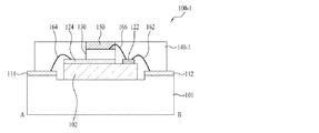
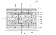
図1は、実施形態に係るランプユニット100の平面図で、図2は、図1に示したラン
プユニット100のAB方向の断面図である。
FIG. 1 is a plan view of the
図1及び図2を参照すると、ランプユニット100は、第1の基板101、第2の基板
102、複数の導電層112、114、122、124、発光素子130、保護層140
、波長変換層150、及び複数のワイヤ162、164、166を含む。
Referring to FIGS. 1 and 2, the
, A
第2の基板102は第1の基板101上に配置することができ、第2の基板102の面
積は第1の基板101の面積より小さくなり得る。他の実施形態においては、第2の基板
102の面積は第1の基板101の面積と同一であり得る。
The
第1の基板101は第1の熱伝導率を有する基板で、第2の基板102は第2の熱伝導
率を有する基板で、第1の熱伝導率は第2の熱伝導率より大きくなり得る。これは、第2
の基板102上に配置される発光素子130から発生する熱を第1の基板101を通して
外部に迅速に放出するためである。
The
This is because the heat generated from the
第1の基板101は、金属基板、例えば、MCPCB(Metal Cored Pr
inted Circuit Board)であり得る。第1の基板101は、熱伝導性
の高い放熱プレートであって、銅(Cu)、アルミニウム(Al)、銀(Ag)、金(A
u)から選ばれたいずれか一つの物質又はそれらの合金で形成することができる。
The
intuit Circuit Board). The
It can be formed of any one material selected from u) or an alloy thereof.
第2の基板102は絶縁基板であり得る。例えば、第2の基板102は、熱伝導率の高
いセラミック基板であり得る。第2の基板102は、窒化物、例えば、AlNで形成する
ことができる。又は、第2の基板102は、陽極酸化層(anodized layer
)を含むこともできる。
The
) Can also be included.
第1の基板101と第2の基板102は多様な形態に形成することができる。
The
一実施形態として、第1の基板101は、所定領域にキャビティ105を有することが
でき、第2の基板102は、第1の基板101のキャビティ105内に配置することがで
きる。このとき、第1の基板101はAl、Cu、Auのうち少なくともいずれか一つを
含むことができ、第2の基板102はAlNを含むことができる。
As an example, the
他の実施形態として、第1の基板101と第2の基板102は、順次積層された積層構
造からなる場合もある。このとき、第1の基板101はAl、Cu、Auのうち少なくと
もいずれか一つを含むことができ、第2の基板102は陽極酸化層を含むことができる。
As another embodiment, the
更に他の実施形態として、第1の基板101と第2の基板102は互いに同一の物質か
らなり、このとき、第1の基板101と第2の基板102はAlN、Al、Cu、Auの
うち少なくともいずれか一つを含むことができる。
As yet another embodiment, the
発光素子130が配置される第2の基板102の上部表面は、平らな平面であるか、凹
状の曲面又は凸状の曲面からなる場合もある。又は、第2の基板102の上部表面は、凹
状の曲面、凸状の曲面、平らな平面のうち少なくとも二つの形状が混合された形態であっ
てもよい。
The upper surface of the
第3の導電層112及び第4の導電層114は、第1の基板101上に互いに離隔する
ように配置することができる。第1の基板101は、第3の導電層112及び第4の導電
層114を含む第1の回路パターンを含むことができる。第3の導電層112及び第4の
導電層114の形状は、図1に示したものに限定されることはなく、多様な形態に具現す
ることができる。
The third
第1の導電層122及び第2の導電層124は、第2の基板102上に互いに離隔する
ように配置することができる。第2の基板102は、第1の導電層122及び第2の導電
層124を含む第2の回路パターンを含むことができる。
The first
発光素子130は第2の基板102上に配置される。発光素子130の数は1個以上で
あり得る。例えば、図1に示したように、発光素子130の数は複数であり、複数の発光
素子130は、互いに離隔するように第2の基板102上に配置することができる。
The
第2の導電層124は複数であり、複数の第2の導電層は互いに離隔するように配置で
きるが、これに限定されることはなく、互いに連結された一つの導電層を形成することも
できる。
There are a plurality of second
図1において第1の導電層122は一つであるが、これに限定されることはなく、複数
であってもよく、複数の第1の導電層は互いに離隔するように配置することができ、それ
ぞれの第1の導電層122にはワイヤ166をボンディングすることができる。
In FIG. 1, the number of the first
図28は、図1に示した発光素子130の一実施形態を示す。
FIG. 28 shows an embodiment of the
図28を参照すると、発光素子130は、第2の電極405、保護層440、電流遮断
層445、発光構造物450、パッシベーション層465、及び第1の電極470を含む
。例えば、発光素子130は、発光ダイオードチップ形態であり得る。
Referring to FIG. 28, the
第2の電極405は、第1の電極470と共に発光構造物450に電源を提供する。第
2の電極405は、支持層410、接合層415、バリア層420、反射層425、及び
オーミック層430を含むことができる。
The
支持層410は、発光構造物450を支持する。支持層410は、金属又は半導体物質
で形成することができる。また、支持層410は、電気伝導性と熱伝導性の高い物質で形
成することができる。例えば、支持層410は、銅(Cu)、銅合金(Cu alloy
)、金(Au)、ニッケル(Ni)、モリブデン(Mo)、及び銅―タングステン(Cu
―W)のうち少なくとも一つを含む金属物質で形成したり、又はSi、Ge、GaAs、
ZnO、SiCのうち少なくとも一つを含む半導体で形成することができる。
The
), Gold (Au), nickel (Ni), molybdenum (Mo), and copper-tungsten (Cu)
-W) formed of a metal material containing at least one of Si, Ge, GaAs,
A semiconductor containing at least one of ZnO and SiC can be used.
接合層415は、支持層410とバリア層420との間に配置することができ、支持層
410とバリア層420を接合させるボンディング層としての役割をすることができる。
接合層415は、金属物質、例えば、In、Sn、Ag、Nb、Pd、Ni、Au、Cu
のうち少なくとも一つを含むことができる。接合層415は、支持層410をボンディン
グ方式で接合するために形成するものであるので、支持層410をめっきや蒸着方法で形
成する場合、接合層415は省略することができる。
The
The
At least one of them. Since the
バリア層420は、反射層425、オーミック層430、及び保護層440の下側に配
置され、接合層415及び支持層410の金属イオンが反射層425及びオーミック層4
30を通過して発光構造物450に拡散されることを防止することができる。例えば、バ
リア層420は、Ni、Pt、Ti、W、V、Fe、Moのうち少なくとも一つを含むこ
とができ、単層又は多層からなり得る。
The
It is possible to prevent the light from passing through 30 and diffusing into the
反射層425は、バリア層420上に配置することができ、発光構造物450から入射
される光を反射させ、光抽出効率を改善することができる。反射層425は、光反射物質
、例えば、Ag、Ni、Al、Rh、Pd、Ir、Ru、Mg、Zn、Pt、Au、Hf
のうち少なくとも一つを含む金属又は合金で形成することができる。
The
The metal or alloy containing at least one of them can be used.
反射層425は、金属又は合金とIZO、IZTO、IAZO、IGZO、IGTO、
AZO、ATOなどの透光性伝導性物質を用いて多層に形成することができ、例えば、I
ZO/Ni、AZO/Ag、IZO/Ag/Ni、AZO/Ag/Niなどで形成するこ
とができる。
The
It can be formed in multiple layers using a light-transmitting conductive material such as AZO or ATO.
It can be formed of ZO / Ni, AZO / Ag, IZO / Ag / Ni, AZO / Ag / Ni, or the like.
オーミック層430は、反射層425と第2の半導体層452との間に配置することが
でき、第2の半導体層452にオーミック接触し、発光構造物450への電源供給を円滑
にすることができる。
The
透光性伝導層と金属を選択的に使用してオーミック層430を形成することができる。
例えば、オーミック層430は、第2の半導体層452とオーミック接触する金属物質、
例えば、Ag、Ni、Cr、Ti、Pd、Ir、Sn、Ru、Pt、Au、Hfのうち少
なくともいずれか一つを含むことができる。
The
For example, the
For example, at least one of Ag, Ni, Cr, Ti, Pd, Ir, Sn, Ru, Pt, Au, and Hf can be included.
保護層440は、第2の電極層405の縁部領域上に配置することができる。例えば、
保護層440は、オーミック層430の縁部領域、反射層425の縁部領域、バリア層4
20の縁部領域、又は支持層410の縁部領域上に配置することができる。
The
The
20 edge regions, or on the edge region of the
保護層440は、発光構造物450と第2の電極層405との間の界面剥離によって発
光素子130の信頼性が低下することを防止することができる。保護層440は、電気絶
縁性物質、例えば、ZnO、SiO2、Si3N4、TiOx(xは正の実数)、又はA
l2O3などで形成することができる。
The
It can be formed of l2O3 or the like.
電流遮断層445は、オーミック層430と発光構造物450との間に配置することが
できる。電流遮断層445の上面は第2の半導体層452と接触し、電流遮断層445の
下面、又は下面と側面はオーミック層430と接触することができる。電流遮断層445
は、垂直方向に第1の電極470と少なくとも一部が空間的にオーバーラップされるよう
に配置することができる。
The
Can be arranged such that at least a portion thereof is spatially overlapped with the
電流遮断層445は、オーミック層430と第2の半導体層452との間に形成したり
、反射層425とオーミック層430との間に形成することができ、これについて限定す
ることはない。
The
発光構造物450は、オーミック層430及び保護層440上に配置することができる
。発光構造物450の側面は、単位チップに区分するアイソレーションエッチング過程で
傾斜面になり得る。発光構造物450は、第2の半導体層452、活性層454、及び第
1の半導体層456を含むことができ、光を発生することができる。
The
第2の半導体層452は、3族―5族、2族―6族などの化合物半導体で具現すること
ができ、これには第2の導電型ドーパントをドーピングすることができる。例えば、第2
の半導体層452は、InxAlyGa1−x−yN(0≦x≦1、0≦y≦1、0≦x
+y≦1)の組成式を有する半導体で形成することができ、これにはp型ドーパント(例
えば、Mg、Zn、Ca、Sr、Ba)をドーピングすることができる。
The
The
+ Y ≦ 1), and can be doped with a p-type dopant (eg, Mg, Zn, Ca, Sr, Ba).
活性層454は、第1の半導体層456及び第2の半導体層452から提供される電子
と正孔の再結合過程で発生するエネルギーによって光を生成することができる。
The
活性層454は、半導体化合物、例えば、3族―5族、2族―6族の化合物半導体で形
成し、単一井戸構造、多重井戸構造、量子線(Quantum―Wire)構造、又は量
子点(Quantum Dot)構造などに形成することができる。活性層454が量子
井戸構造である場合は、InxAlyGa1−x−yN(0≦x≦1、0≦y≦1、0≦
x+y≦1)の組成式を有する井戸層と、InaAlbGa1−a−bN(0≦a≦1、
0≦b≦1、0≦a+b≦1)の組成式を有する障壁層とを備える単一又は量子井戸構造
にすることができる。井戸層は、障壁層のエネルギーバンドギャップより低いバンドギャ
ップを有する物質であり得る。
The
a well layer having a composition formula of x + y ≦ 1) and InaAlbGa1-a-bN (0 ≦ a ≦ 1,
And a single or quantum well structure including a barrier layer having a composition formula of 0 ≦ b ≦ 1, 0 ≦ a + b ≦ 1). The well layer may be a material having a band gap lower than the energy band gap of the barrier layer.
第1の半導体層456は、3族―5族、2族―6族などの化合物半導体で具現すること
ができ、これには第1の導電型ドーパントをドーピングすることができる。例えば、第1
の半導体層456は、InxAlyGa1−x−yN(0≦x≦1、0≦y≦1、0≦x
+y≦1)の組成式を有する半導体で形成することができ、これにはn型ドーパント(例
えば、Si、Ge、Sn、Se、Teなど)をドーピングすることができる。
The
The
+ Y ≦ 1), and can be doped with an n-type dopant (eg, Si, Ge, Sn, Se, Te, etc.).
発光素子130は、発光構造物450の第1の半導体層456、活性層454、及び第
2の半導体層452の組成によって青色光、赤色光、緑色光、及び黄色光のうちいずれか
一つを放出することができる。
The light-emitting
パッシベーション層465は、発光構造物450を電気的に保護するために発光構造物
450の側面に配置することができる。パッシベーション層465は、第1の半導体層4
56の上面一部又は保護層440の上面にも配置することができる。パッシベーション層
465は、絶縁物質、例えば、SiO2、SiOx、SiOxNy、Si3N4、又はA
l2O3で形成することができる。
The
The upper surface part of 56 or the upper surface of the
It can be formed of l2O3.
第1の電極470は、第1の半導体層456上に配置することができる。第1の電極4
70は、所定のパターン形状であり得る。第1の電極470は、ワイヤボンディングのた
めのパッド部、及びパッド部から拡張される枝電極(図示せず)を含むことができる。
The
70 may be a predetermined pattern shape. The
第1の半導体層456の上面には、光抽出効率を増加させるためにラフネスパターン(
図示せず)を形成することができる。また、光抽出効率を増加させるために、第1の電極
470の上面にもラフネスパターン(図示せず)を形成することができる。
On the upper surface of the
(Not shown) can be formed. In addition, a roughness pattern (not shown) can be formed on the upper surface of the
発光素子130は、第1の導電層122と第2の導電層124に電気的に連結すること
ができる。発光素子130の数が複数であるとき、複数の発光素子は、第1の導電層12
2と第2の導電層124に電気的に連結することができる。
The
2 and the second
発光素子130の第2の電極405は、共晶ボンディング(eutectic bon
ding)又はダイボンディングを用いて第2の基板102上に配置された第2の導電層
124にボンディングし、第2の導電層124と電気的に連結することができる。
The
ing) or die bonding to the second
ワイヤ166は、発光素子130の第1の電極470と第2の基板102上に配置され
た第1導電層122とを電気的に連結することができる。ワイヤ166の数は1個以上で
あり得る。
The
ワイヤ162は、第2の基板102上に配置された第1の導電層122と第1の基板1
01上に配置された第3の導電層112とを電気的に連結することができる。ワイヤ16
2の数は1個以上であり得る。
The
The third
The number of 2 can be one or more.
ワイヤ164は、第2の基板102上に配置された第2の導電層124と第1の基板1
01上に設けられた第4の導電層114とを電気的に連結することができる。ワイヤ16
4の数は1個以上であり得る。
The
The fourth
The number of 4 can be one or more.
波長変換層150は、発光素子130の上部に位置し、発光素子130から発生する光
の波長を変化させることができる。波長変換層150は、エポキシ又はシリコンなどの無
色透明な高分子樹脂及び蛍光体を含むことができる。波長変換層150は、赤色蛍光体、
緑色蛍光体、及び黄色蛍光体のうち少なくとも一つを含むことができる。波長変換層15
0は、ワイヤ166の一部を覆うことができる。ワイヤ166の数が複数であるとき、保
護層は、複数のワイヤのそれぞれの一部を覆うことができる。
The
At least one of a green phosphor and a yellow phosphor may be included. Wavelength conversion layer 15
0 can cover part of the
保護層140は、発光素子130及び各ワイヤ162〜166を包囲するように第1の
基板101及び第2の基板102上に配置される。保護層140は、第1の基板101の
キャビティ105に充填することができる。保護層140の上部面は、ワイヤ166の最
高点より高く位置し得る。
The
保護層140は、各ワイヤ162〜166を包囲し、各ワイヤ162〜166が外部に
露出したり、突出することを防止することができる。保護層を備えることによって、実施
形態は、ワイヤ(例えば、166)が衝撃又は圧力によって破損又は変形したり、空気な
どによって腐食することを防止することができ、その結果、発光素子130の破損又は誤
動作を防止することができる。
The
保護層140は、光を反射できる非伝導性モールディング部材、例えば、ホワイトシリ
コンからなり得るが、これに限定されることはない。
The
保護層140は、発光素子130、例えば、図1に示した複数の発光素子と密着し、発
光素子130から照射される光を直ぐ反射させるので、実施形態は、空気又は第1の基板
101及び第2のと基板102による吸収及び透過によって発生する光損失を減少させる
ことができ、発光効率を向上させることができる。
The
図3は、第1の実施形態に係る波長変換層150とワイヤ166の拡大図である。
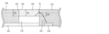
FIG. 3 is an enlarged view of the
図3を参照すると、保護層140は、波長変換層150の側面152及び発光素子13
0の側面と接することができ、波長変換層150の側面152を覆うことができる。
Referring to FIG. 3, the
The side surface of the
波長変換層150の上部面154は平らであり、保護層140から露出し得る。
The
波長変換層150の上部面154は、保護層140の上部面142と同一の平面上に位
置し得る。発光素子130の上面から波長変換層150の上部面154までの高さH2は
、発光素子130の上面から保護層140の上部面142までの高さH3と同一であり得
る(H2=H3)。
The
ワイヤ166を保護するために、波長変換層150の上部面154及び保護層140の
上部面142は、ワイヤ166の最高点T1より高く位置し得る。
In order to protect the
発光素子130の上面から波長変換層150の上部面154及び保護層140の上部面
142までの高さは、少なくとも50μmを超えることができる。これは、実質的に工程
上可能なワイヤ166の最高点T1の最低高さH1が約50μmであるためである。した
がって、発光素子130の上面から波長変換層150の上部面154及び保護層140の
上部面142までの高さが50μm以下である場合、ワイヤ166が保護層140から露
出し得る。
The height from the upper surface of the
発光素子130の上面から波長変換層150の上部面154までの高さH2は、発光素
子130の上面からワイヤ166の最高点T1までの高さH1より高くなり得る(H2>
H1)。これは、ワイヤ166の露出を防止するためである。
A height H2 from the upper surface of the
H1). This is to prevent the
図4は、第2の実施形態に係る波長変換層150―1とワイヤ166の拡大図である。
FIG. 4 is an enlarged view of the wavelength conversion layer 150-1 and the
図4を参照すると、波長変換層150―1の上部面154―1は、保護層140の上部
面142より高く位置し得る。波長変換層150―1の上部面154―1は、保護層14
0の上部面142から突出した構造であり得る。
Referring to FIG. 4, the upper surface 154-1 of the wavelength conversion layer 150-1 may be positioned higher than the
The structure may protrude from the
発光素子130の上面から波長変換層150―1の上部面154―1までの高さH4は
、発光素子130の上面から保護層140の上部面142までの高さH3より高くなり得
る(H4>H3)。
A height H4 from the upper surface of the
図5は、第3の実施形態に係る波長変換層150―2とワイヤ166の拡大図である。
FIG. 5 is an enlarged view of the wavelength conversion layer 150-2 and the
図5を参照すると、波長変換層150―2の上部面154―2は、保護層140の上部
面142より低く位置し得る。発光素子130の上面から波長変換層150―2の上部面
154―2までの高さH5は、発光素子130の上面から保護層140の上部面142ま
での高さH3より低く、ワイヤ166の最高点T1の高さH1より高くなり得る(H1<
H5<H3)。
Referring to FIG. 5, the upper surface 154-2 of the wavelength conversion layer 150-2 may be positioned lower than the
H5 <H3).
図6は、第4の実施形態に係る波長変換層150―3とワイヤ166の拡大図である。
FIG. 6 is an enlarged view of the wavelength conversion layer 150-3 and the
図6を参照すると、波長変換層150―3の上部面154―3は曲面であり得る。例え
ば、波長変換層150―3の上部面154―3はドーム状又は半球状であり得る。波長変
換層150―3の上部面154―3が曲面であるので、第4の実施形態は、発光素子13
0から照射される光を屈折させることによって指向角を向上させることができる。
Referring to FIG. 6, the upper surface 154-3 of the wavelength conversion layer 150-3 may be a curved surface. For example, the upper surface 154-3 of the wavelength conversion layer 150-3 may be dome-shaped or hemispherical. Since the upper surface 154-3 of the wavelength conversion layer 150-3 is a curved surface, the fourth embodiment has the light-emitting element 13.
The directivity angle can be improved by refracting the light irradiated from zero.
発光素子130の数が複数であるとき、図3ないし図6での説明は、図1に示した複数
の発光素子に同一に適用することができる。
When there are a plurality of
図7は、一実施形態に係る波長変換層150を示す。
FIG. 7 shows a
図7を参照すると、発光素子130の数が複数であるとき、波長変換層150は、各発
光素子130がそれぞれ位置する各領域S1〜S4に対応するように位置し得る。波長変
換層150は、複数の互いに離隔する各部分(例えば、150―a、150―b、150
―c、150―d)を含むことができ、各部分(例えば、150―a、150―b、15
0―c、150―d)のそれぞれは、図1に示した各発光素子のうちいずれか一つに対応
するように位置し得る。
Referring to FIG. 7, when the number of the
-C, 150-d) and each part (eg 150-a, 150-b, 15
Each of 0-c and 150-d) may be positioned to correspond to any one of the light-emitting elements shown in FIG.
図8は、他の実施形態に係る波長変換層150'を示す。
FIG. 8 shows a
図8を参照すると、発光素子130の数が複数であるとき、波長変換層150'は、図
1に示した各発光素子がそれぞれ位置する領域及び隣接する2個の発光素子の間の領域を
全て合わせた領域S4に対応するように位置することができ、一つの部分からなり得る。
Referring to FIG. 8, when the number of the
図9は、他の実施形態に係るランプユニット100―1の断面図である。図2と同一の
図面符号は同一の構成を示し、同一の構成についての説明は、重複を避けるために簡略に
したり省略する。
FIG. 9 is a cross-sectional view of a lamp unit 100-1 according to another embodiment. The same reference numerals as those in FIG. 2 denote the same components, and the description of the same components is simplified or omitted to avoid duplication.
図9を参照すると、ランプユニット100―1が図2に示した実施形態のランプユニッ
ト100と異なる点は、保護層140―1が透光性である点にある。
Referring to FIG. 9, the lamp unit 100-1 is different from the
すなわち、保護層140―1は、光を透過できる非伝導性モールディング部材からなり
得る。例えば、保護層140―1は、シリコン樹脂、エポキシ樹脂、ガラス、ガラスセラ
ミック、ポリエステル樹脂、アクリル樹脂、ウレタン樹脂、ナイロン樹脂、ポリアミド樹
脂、ポリイミド樹脂、塩化ビニル樹脂、ポリカーボネート樹脂、ポリエチレン樹脂、テフ
ロン(登録商標)樹脂、ポリスチレン樹脂、ポリプロピレン樹脂、ポリオレフィン樹脂な
どからなり得る。
That is, the protective layer 140-1 may be made of a non-conductive molding member that can transmit light. For example, the protective layer 140-1 is made of silicon resin, epoxy resin, glass, glass ceramic, polyester resin, acrylic resin, urethane resin, nylon resin, polyamide resin, polyimide resin, vinyl chloride resin, polycarbonate resin, polyethylene resin, Teflon ( (Registered trademark) resin, polystyrene resin, polypropylene resin, polyolefin resin and the like.
図9に示した保護層140―1は、上述した保護層140と材質において異なるだけで
、残りは上述した通りであり得る。
The protective layer 140-1 shown in FIG. 9 differs from the
図10は、他の実施形態に係るランプユニット100―2の平面図で、図11は、図1
0に示したランプユニット100―2のAB方向の断面図である。図2と同一の図面符号
は同一の構成を示し、同一の構成についての説明は、重複を避けるために簡略にしたり省
略する。
FIG. 10 is a plan view of a lamp unit 100-2 according to another embodiment, and FIG.
2 is a cross-sectional view in the AB direction of the lamp unit 100-2 shown in FIG. The same reference numerals as those in FIG. 2 denote the same components, and the description of the same components is simplified or omitted to avoid duplication.
図10及び図11を参照すると、ランプユニット100―2は、図2に示した実施形態
のランプユニット100にレンズ210をさらに含む構造である。
Referring to FIG. 10 and FIG. 11, the lamp unit 100-2 has a structure further including a
レンズ210は、各発光素子130にそれぞれ対応するように波長変換層150及び保
護層140上に配置することができる。レンズ210は、対応する発光素子から照射され
る光を屈折させることができ、ランプユニット100―2の光経路を調節することができ
る。
The
発光素子130の数が複数であるとき、図10では、各発光素子のそれぞれに対応する
レンズ210を示したが、他の実施形態では、各発光素子の全体を覆う一つのレンズに具
現することもできる。
When the number of the
図12は、他の実施形態に係るランプユニット100―3の平面図で、図13は、図1
2に示したランプユニット100―3のAB方向の断面図である。図2と同一の図面符号
は同一の構成を示し、同一の構成についての説明は、重複を避けるために簡略にしたり省
略する。
FIG. 12 is a plan view of a lamp unit 100-3 according to another embodiment, and FIG.
FIG. 3 is a cross-sectional view in the AB direction of the lamp unit 100-3 shown in FIG. The same reference numerals as those in FIG. 2 denote the same components, and the description of the same components is simplified or omitted to avoid duplication.
図12及び図13を参照すると、ランプユニット100―3は、第1の基板101、第
2の基板102、複数の導電層112、114、122、124、発光素子130―1、
保護層140、及び複数のワイヤ162、164、166を含む。
12 and 13, the lamp unit 100-3 includes a
A
図12及び図13を参照すると、図2に示した実施形態では、チップ形態の発光素子1
30と、発光素子130上に位置する波長変換層150とを備えるが、ランプユニット1
00―3は、図2に示した実施形態のランプユニット100の発光素子130と波長変換
層150が一つのチップに具現された発光素子130―1を含む。
Referring to FIG. 12 and FIG. 13, in the embodiment shown in FIG.
30 and a
00-3 includes a light emitting device 130-1 in which the
例えば、発光素子130は、青色光、緑色光、赤色光、及び黄色光のうちいずれか一つ
を放出することができ、発光素子130―1は白色光を放出することができる。
For example, the
図29は、図13に示した発光素子130―1の一実施形態を示す。図28と同一の図
面符号は同一の構成を示し、同一の構成についての説明は、重複を避けるために簡略にし
たり省略する。
FIG. 29 shows an embodiment of the light-emitting element 130-1 shown in FIG. The same reference numerals as those in FIG. 28 denote the same components, and the description of the same components is simplified or omitted to avoid duplication.
図29を参照すると、発光素子130―1は波長変換層480をさらに含む。
Referring to FIG. 29, the light emitting device 130-1 further includes a
波長変換層480は、第1の半導体層456上に配置することができ、第1の電極47
0を露出させることができる。
The
0 can be exposed.
例えば、波長変換層480は、エポキシ又はシリコンなどの無色透明な高分子樹脂と蛍
光体の混合物であって、高分子樹脂と蛍光体の混合物を第1の半導体層456上にコンフ
ォーマルコーティング(conformal coating)することによって波長変
換層480を形成することができる。波長変換層480は、ワイヤボンディングのために
第1の電極470のパッド部(図示せず)を露出させることができる。
For example, the
保護層140の上部面は、第2の基板102上に配置される導電層122にボンディン
グされるワイヤ166の最高点より高く位置し得る。保護層140は、各ワイヤ162〜
166を包囲し、各ワイヤ162〜166が外部に露出したり、突出することを防止する
ことができる。
The upper surface of the
166 can be surrounded and each wire 162-166 can be prevented from being exposed to the outside or protruding.
保護層140は、発光素子130―1の側面と接することができ、発光素子130―1
の上面は保護層140から露出し得る。
The
The upper surface of the
保護層140の上部面は、発光素子130―1の上部面と同一の平面上に位置し得る。
すなわち、発光素子130―1の上面の高さは、保護層140の上部面の高さと同一であ
り得る。このとき、発光素子130―1の上面は波長変換層480の上部面であり得る。
The upper surface of the
That is, the height of the upper surface of the light emitting device 130-1 may be the same as the height of the upper surface of the
図14は、他の実施形態に係るランプユニット100―4の断面図である。図13と同
一の図面符号は同一の構成を示し、同一の構成についての説明は、重複を避けるために簡
略にしたり省略する。
FIG. 14 is a cross-sectional view of a lamp unit 100-4 according to another embodiment. The same reference numerals as those in FIG. 13 denote the same components, and the description of the same components is simplified or omitted to avoid duplication.
図14を参照すると、ランプユニット100―4が図13に示した実施形態のランプユ
ニット100―3と異なる点は、保護層140―1が透光性モールディング部材であると
いう点にある。図14に示した保護層140―1は、上述した保護層140と材質におい
て異なるだけで、残りは上述した通りであり得る。
Referring to FIG. 14, the lamp unit 100-4 is different from the lamp unit 100-3 of the embodiment shown in FIG. 13 in that the protective layer 140-1 is a translucent molding member. The protective layer 140-1 shown in FIG. 14 is different from the
図15は、他の実施形態に係るランプユニット100―5の平面図で、図16は、図1
5に示したランプユニット100―5のAB方向の断面図である。
FIG. 15 is a plan view of a lamp unit 100-5 according to another embodiment, and FIG.
6 is a cross-sectional view in the AB direction of the lamp unit 100-5 shown in FIG.
図15及び図16を参照すると、ランプユニット100―5は、図13に示した実施形
態のランプユニット100―3にレンズ210をさらに含む構造である。
Referring to FIGS. 15 and 16, the lamp unit 100-5 has a structure further including a
レンズ210は、各発光素子130―1にそれぞれ対応するように保護層140上に配
置することができる。レンズ210は、対応する発光素子から照射される光を屈折させる
ことができ、ランプユニット100―5の光経路を調節することができる。
The
発光素子130―1の数が複数であるとき、図15では、各発光素子に対応するレンズ
210を示したが、他の実施形態では、各発光素子の全体を覆う一つのレンズに具現する
こともできる。
When the number of the light emitting elements 130-1 is plural, in FIG. 15, the
図17は、他の実施形態に係るランプユニット200の平面図で、図18は、図17に
示したランプユニット200のCD方向の断面図である。図1及び図2と同一の図面符号
は同一の構成を示し、同一の構成についての説明は、重複を避けるために簡略にしたり省
略する。
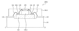
FIG. 17 is a plan view of a
図17及び図18を参照すると、ランプユニット200は、第1の基板101、第2の
基板102、複数の導電層112、114、122、124―1、発光素子130―2、
保護層140、波長変換層150、及び複数のワイヤ162、164、166、168を
含む。
Referring to FIGS. 17 and 18, the
A
ランプユニット200が図2に示したランプユニット100と異なる点は、発光素子1
30―2が水平型発光ダイオードである点と、これによる発光素子130―2と各導電層
112、114、122、124―1との電気的連結構造にある。
The
30-2 is a horizontal light-emitting diode, and the light-emitting element 130-2 and the electrically
発光素子130―2の数が複数であるとき、図17に示した各発光素子は第2の基板1
02上に配置することができる。
When the number of the light emitting elements 130-2 is plural, each light emitting element shown in FIG.
02 can be arranged.
図30は、図18に示した発光素子130―2の一実施形態を示す。 FIG. 30 shows an embodiment of the light emitting device 130-2 shown in FIG.
図30を参照すると、発光素子130―2は、基板310、発光構造物450、伝導層
330、第1の電極342、及び第2の電極344を含む。
Referring to FIG. 30, the light emitting device 130-2 includes a
基板310は、半導体物質成長に適した物質、すなわち、キャリアウエハーで形成する
ことができる。また、基板310は、熱伝導性に優れた物質で形成することができ、伝導
性基板又は絶縁性基板であり得る。例えば、基板310は、サファイア(Al2O3)、
GaN、SiC、ZnO、Si、GaP、InP、Ga2O3、GaAsのうち少なくと
も一つを含む物質で形成することができる。このような基板310の上面には凹凸パター
ンを形成することができる。
The
A material containing at least one of GaN, SiC, ZnO, Si, GaP, InP, Ga2O3, and GaAs can be used. An uneven pattern can be formed on the upper surface of the
また、基板310上には、2族ないし6族元素の化合物半導体を用いた層又はパターン
、例えば、ZnO層(図示せず)、バッファー層(図示せず)、アンドープ半導体層(図
示せず)のうち少なくとも一つの層を形成することができる。バッファー層又はアンドー
プ半導体層は、3族―5族元素の化合物半導体を用いて形成することができ、バッファー
層は基板との格子定数の差を減少させ、アンドープ半導体層は、ドーピングしないGaN
系半導体で形成することができる。
Further, on the
It can be formed of a system semiconductor.
発光構造物450は、光を発生する半導体層であって、第1の半導体層456、活性層
454、及び第2の半導体層452を含むことができる。第1の半導体層456、活性層
454、及び第2の半導体層452は、図28を参照して説明した通りであり得る。発光
素子130―2は、青色光、緑色光、赤色光、及び黄色光のうちいずれか一つを放出する
ことができる。
The
発光構造物450は、第2の半導体層452、活性層454及び第1の半導体層456
の一部が除去されることによって、第1の半導体層456の一部を露出させることができ
る。
The
By removing a part of the
伝導層330は、全反射を減少させるだけでなく、透光性が良いので、活性層454か
ら第2の半導体層452に放出される光の抽出効率を増加させることができる。
The
伝導層330は、透明伝導性酸化物、例えば、ITO(Indium Tin Oxi
de)、TO(Tin Oxide)、IZO(Indium Zinc Oxide)
、ITZO(Indium Tin Zinc Oxide)、IAZO(Indium
Aluminum Zinc Oxide)、IGZO(Indium Galliu
m Zinc Oxide)、IGTO(Indium Gallium Tin Ox
ide)、AZO(Aluminum Zinc Oxide)、ATO(Antimo
ny tin Oxide)、GZO(Gallium Zinc Oxide)、Ir
Ox、RuOx、RuOx/ITO、Ni、Ag、Ni/IrOx/Au、及びNi/I
rOx/Au/ITOのうち一つ以上を用いて単層又は多層からなり得る。
The
de), TO (Tin Oxide), IZO (Indium Zinc Oxide)
, ITZO (Indium Tin Zinc Oxide), IAZO (Indium
Aluminum Zinc Oxide), IGZO (Indium Galliu)
m Zinc Oxide), IGTO (Indium Gallium Tin Ox)
ide), AZO (Aluminum Zinc Oxide), ATO (Antimo)
ny tin Oxide), GZO (Gallium Zinc Oxide), Ir
Ox, RuOx, RuOx / ITO, Ni, Ag, Ni / IrOx / Au, and Ni / I
One or more of rOx / Au / ITO may be used to form a single layer or multiple layers.
第1の電極342は、露出する第1の半導体層456上に配置することができ、第2の
電極344は、伝導層330上に配置することができる。
The
第1の導電層122と第4の導電層124―1は、第2の基板102上に互いに離隔す
るように位置し、発光素子130―2は、第1の導電層122と第4の導電層124―1
に電気的に連結することができる。
The first
Can be electrically coupled.
発光素子130―2の基板310は第2の基板102にボンディングすることができる
。
The
ワイヤ166は、発光素子130―2の第1の電極342と第2の基板102上に配置
された第1の導電層122とを電気的に連結することができる。ワイヤ168は、発光素
子130―2の第2の電極344と第2の基板102上に配置された第4の導電層124
―1とを電気的に連結することができる。
The
-1 can be electrically connected.
各ワイヤ166、168を保護するために、波長変換層150の上部面及び保護層14
0の上部面は、各ワイヤ166、168のそれぞれの最高点T1より高く位置し得る。
In order to protect each
The top surface of zero may be located higher than the respective highest point T1 of each
図19は、他の実施形態に係るランプユニット200―1を示す。図18と同一の図面
符号は同一の構成を示し、同一の構成についての説明は、重複を避けるために簡略にした
り省略する。
FIG. 19 shows a lamp unit 200-1 according to another embodiment. The same reference numerals as those in FIG. 18 denote the same components, and description of the same components is simplified or omitted to avoid duplication.
図19を参照すると、ランプユニット200―1が図18に示した実施形態のランプユ
ニット200と異なる点は、保護層140―1が透光性である点にある。
Referring to FIG. 19, the lamp unit 200-1 is different from the
図20は、他の実施形態に係るランプユニット200―2の平面図で、図21は、図2
0に示したランプユニット200―2のCD方向の断面図である。図18と同一の図面符
号は同一の構成を示し、同一の構成についての説明は、重複を避けるために簡略にしたり
省略する。
20 is a plan view of a lamp unit 200-2 according to another embodiment, and FIG.
FIG. 3 is a cross-sectional view in the CD direction of the lamp unit 200-2 shown in FIG. The same reference numerals as those in FIG. 18 denote the same components, and description of the same components is simplified or omitted to avoid duplication.
図20及び図21を参照すると、ランプユニット200―2は、図18に示した実施形
態のランプユニット200にレンズ210をさらに含む構造である。レンズ210は、各
発光素子130―2にそれぞれ対応するように波長変換層150及び保護層140上に配
置することができる。レンズ210は、対応する発光素子130―2から照射される光を
屈折させることができ、ランプユニット200―2の光経路を調節することができる。
Referring to FIGS. 20 and 21, the lamp unit 200-2 has a structure further including a
図22は、他の実施形態に係るランプユニット200―3の平面図で、図23は、図2
2に示したランプユニット200―3のCD方向の断面図である。図17及び図18と同
一の図面符号は同一の構成を示し、同一の構成についての説明は、重複を避けるために簡
略にしたり省略する。
FIG. 22 is a plan view of a lamp unit 200-3 according to another embodiment, and FIG.
FIG. 3 is a cross-sectional view in the CD direction of the lamp unit 200-3 shown in FIG. The same reference numerals as those in FIGS. 17 and 18 indicate the same configuration, and the description of the same configuration is simplified or omitted to avoid duplication.
図22及び図23を参照すると、ランプユニット200―3は、第1の基板101、第
2の基板102、複数の導電層112、114、122、124―1、発光素子130―
3、保護層140、及び複数のワイヤ162、164、166、168を含む。
22 and 23, the lamp unit 200-3 includes a
3, a
図22及び図23を参照すると、図18に示した実施形態では、チップ形態の発光素子
130―2と、発光素子130―2上に位置する波長変換層150とを備えるが、ランプ
ユニット200―3は、図18に示した実施形態のランプユニット200の発光素子13
0―2と波長変換層150が一つのチップに具現された発光素子130―3を含む。
Referring to FIGS. 22 and 23, the embodiment shown in FIG. 18 includes a light emitting element 130-2 in a chip form and a
0-2 and the
例えば、発光素子130―2は、青色光、緑色光、赤色光、及び黄色光のうちいずれか
一つを放出することができ、発光素子130―3は白色光を放出することができる。
For example, the light emitting element 130-2 can emit any one of blue light, green light, red light, and yellow light, and the light emitting element 130-3 can emit white light.
図31は、図23に示した発光素子130―3の一実施形態を示す。図30と同一の図
面符号は同一の構成を示し、同一の構成についての説明は、重複を避けるために簡略にし
たり省略する。
FIG. 31 shows an embodiment of the light emitting device 130-3 shown in FIG. The same reference numerals as those in FIG. 30 denote the same components, and the description of the same components is simplified or omitted to avoid duplication.
図31を参照すると、発光素子130―3は波長変換層350をさらに含む。
Referring to FIG. 31, the light emitting device 130-3 further includes a
波長変換層350は、第2の半導体層452上に配置することができ、第2の電極34
4を露出させることができる。
The
4 can be exposed.
保護層140の上部面は、発光素子130―3の上面と同一の平面上に位置し得る。発
光素子130―3の上面の高さは、保護層140の上部面の高さと同一であり得る。この
とき、発光素子130―3の上面は、波長変換層350の上部面であり得る。
The upper surface of the
保護層140は、発光素子130―3の側面と接することができ、発光素子130―3
の上面は保護層140から露出し得る。
The
The upper surface of the
各ワイヤ166、168の最高点の高さは、発光素子130―3の上面の高さ及び保護
層140の上部面の高さより低いので、実施形態は、各ワイヤ166、168の破損及び
変形を防止することができる。
Since the height of the highest point of each
図24は、他の実施形態に係るランプユニット200―4の断面図である。図23と同
一の図面符号は同一の構成を示し、同一の構成についての説明は、重複を避けるために簡
略にしたり省略する。
FIG. 24 is a cross-sectional view of a lamp unit 200-4 according to another embodiment. The same reference numerals as those in FIG. 23 denote the same components, and the description of the same components is simplified or omitted to avoid duplication.
図24を参照すると、図23に示したランプユニット200―3の保護層140は反射
部材である一方、ランプユニット200―4の保護層140―1は透光性であり得る。
Referring to FIG. 24, the
図25は、他の実施形態に係るランプユニット200―5の平面図で、図26は、図2
5に示したランプユニット200―5のCD方向の断面図である。
FIG. 25 is a plan view of a lamp unit 200-5 according to another embodiment, and FIG.
6 is a cross-sectional view of the lamp unit 200-5 shown in FIG.
図22及び図23と同一の図面符号は同一の構成を示し、同一の構成についての説明は
、重複を避けるために簡略にしたり省略する。
The same reference numerals as those in FIGS. 22 and 23 indicate the same structure, and the description of the same structure is simplified or omitted to avoid duplication.
図25及び図26を参照すると、発光素子130―3から照射される光を屈折させ、光
経路を調節するために、ランプユニット200―5は、図23に示した実施形態のランプ
ユニット200―3にレンズ210をさらに含む構成であり得る。
Referring to FIGS. 25 and 26, in order to refract the light emitted from the light emitting element 130-3 and adjust the light path, the lamp unit 200-5 includes the lamp unit 200- of the embodiment shown in FIG. 3 may further include a
図27は、他の実施形態に係るランプユニットの断面図である。図27に示した実施形
態は、図1に示したランプユニット100の変形例であって、モールディング固定部19
0をさらに含むことができる。
FIG. 27 is a cross-sectional view of a lamp unit according to another embodiment. The embodiment shown in FIG. 27 is a modification of the
0 can further be included.
図27を参照すると、モールディング固定部190は、保護層140の外周面に接する
ように第1の基板101及び複数の導電層112、114、122、124上に配置する
ことができ、保護層140の縁部を支持及び固定することができる。
Referring to FIG. 27, the
モールディング固定部190は、各発光素子150の周囲を取り囲むように第1の基板
101及び複数の導電層112、114、122、124上に配置することができ、モー
ルディング固定部190の内部にモールディング部材を吐出し、吐出されたモールディン
グ部材を硬化させることによって保護層140を形成することができる。このとき、モー
ルディング固定部190は、吐出されたモールディング部材が溢れることを防止すること
ができ、硬化後には保護層140を支持する役割をすることができる。
The
モールディング固定部190の形状は、形成しようとする保護層の形状に応じて決定す
ることができる。例えば、モールディング固定部190は、円状、楕円状、又は四角形状
などの多角形状であり得るが、これに限定されることはない。
The shape of the
モールディング固定部190は、他の実施形態のランプユニット100―2〜100―
5、200、200―1〜200―5にも追加して適用することができる。
The
5, 200, 200-1 to 200-5 can be additionally applied.
図32は、実施形態に係る車両用ヘッドランプ800の断面図である。
FIG. 32 is a cross-sectional view of the
図32を参照すると、ヘッドランプ800は、ランプユニット801、リフレクタ80
2、シェード803、及びレンズ804を含む。
Referring to FIG. 32, a
2, a
ランプユニット801は、各実施形態のランプユニット100、100―1〜100―
5、200、200―1〜200―5のうちいずれか一つであり、光を発生することがで
きる。
The
5, 200, 200-1 to 200-5, and can generate light.
リフレクタ802は、ランプユニット801から照射される光を一定方向に反射させる
ことができる。シェード803は、リフレクタ802とレンズ804との間に配置するこ
とができ、リフレクタ802によって反射されてレンズ804に向かう光の一部分を遮断
又は反射し、設計者が望む配光パターンをなすようにする部材である。
The
ここで、レンズ804に隣接するシェード803の一側部803―1とランプユニット
801に隣接するシェード803の他側部803―2は高さが異なり得る。
Here, the height of the one side portion 803-1 of the
そして、ランプユニット801から照射された光は、リフレクタ802及びシェード8
03から反射された後、レンズ804を透過して車両の前方に進行することができる。こ
のとき、レンズ804は、リフレクタ802によって反射された光を屈折させることがで
きる。
The light emitted from the
After being reflected from 03, the light can pass through the
図33は、他の実施形態に係る車両のヘッドランプを示す。 FIG. 33 shows a headlamp of a vehicle according to another embodiment.
図33を参照すると、車両用ヘッドランプ900は、ランプユニット910及びライト
ハウジング920を含むことができる。
Referring to FIG. 33, the
ランプユニット910は、上述した各実施形態のランプユニット100、100―1〜
100―5、200、200―1〜200―5のうち少なくとも一つを含むことができる
。
The
100-5, 200, 200-1 to 200-5 may be included.
ライトハウジング920は、ランプユニット910を収納することができ、透光性材質
からなり得る。車両用ライトハウジング920は、装着される車両部位及びデザインに応
じて屈曲を含むことができる。
The
上述した車両用ヘッドランプ800、900は、実施形態に係るランプユニットを備え
ることによって、光効率を向上させることができる。
The
以上各実施形態で説明した特徴、構造、効果などは、本発明の少なくとも一つの実施形
態に含まれるものであって、必ずしも一つの実施形態のみに限定されるものではない。さ
らに、各実施形態で例示した特徴、構造、効果などは、各実施形態の属する分野で通常の
知識を有する者であれば他の実施形態に対しても組み合わせ又は変形によって実施可能で
ある。したがって、このような組み合わせと変形と関係した各内容は、本発明の範囲に含
まれるものとして解釈すべきであろう。
The features, structures, effects, and the like described in the above embodiments are included in at least one embodiment of the present invention, and are not necessarily limited to only one embodiment. Furthermore, the features, structures, effects, and the like exemplified in each embodiment can be implemented by combining or modifying other embodiments as long as they have ordinary knowledge in the field to which each embodiment belongs. Therefore, the contents related to such combinations and modifications should be construed as being included in the scope of the present invention.
100 ランプユニット
101 第1の基板
102 第2の基板
105 キャビティ
112、114、122、124 導電層
140 保護層
150 波長変換層
162、164、166 ワイヤ
100
Claims (9)
前記第1の基板上に配置される第2の基板と、
前記第2の基板上に配置される発光素子と、
前記第2の基板上に配置される第1の導電層及び第2の導電層と、
前記第1の導電層及び前記第2の導電層のうち少なくとも一つと前記発光素子とを電気的に連結する少なくとも一つのワイヤと、
前記発光素子上に配置され、前記発光素子から照射される光の波長を変換する波長変換層と、
前記発光素子及び前記少なくとも一つのワイヤを包囲するように前記第1の基板及び前記第2の基板上に配置される保護層と、を含み、
前記波長変換層の上面は前記保護層から露出し、
前記保護層は、前記発光素子の側面及び前記波長変換層の側面と接し、
前記保護層の上面及び前記波長変換層の上面は、それぞれ前記少なくとも一つのワイヤの最高点より高く位置し、
前記発光素子の数は複数であり、各発光素子は互いに離隔するように位置し、前記波長変換層は複数の部分を含み、前記複数の部分は、それぞれ前記各発光素子のうちいずれか一つに対応するように位置する、ランプユニット。 A first substrate and a second substrate disposed on the first substrate;
A light emitting device disposed on the second substrate;
A first conductive layer and a second conductive layer disposed on the second substrate;
At least one wire electrically connecting at least one of the first conductive layer and the second conductive layer and the light emitting element;
A wavelength conversion layer that is disposed on the light emitting element and converts a wavelength of light emitted from the light emitting element;
A protective layer disposed on the first substrate and the second substrate so as to surround the light emitting element and the at least one wire,
The upper surface of the wavelength conversion layer is exposed from the protective layer,
The protective layer is in contact with the side surface of the light emitting element and the side surface of the wavelength conversion layer,
The upper surface of the protective layer and the upper surface of the wavelength conversion layer are each positioned higher than the highest point of the at least one wire ,
The light emitting device includes a plurality of light emitting devices, the light emitting devices are spaced apart from each other, the wavelength conversion layer includes a plurality of portions, and each of the plurality of portions is one of the light emitting devices. The lamp unit is located to correspond to the .
前記保護層の上面は、前記波長変換層の上面の縁部から離隔する、請求項1項に記載のランプユニット。 The wavelength conversion layer covers a portion of the at least one wire;
The lamp unit according to claim 1, wherein an upper surface of the protective layer is separated from an edge portion of the upper surface of the wavelength conversion layer.
前記発光素子は、青色光、緑色光、赤色光、及び黄色光のうちいずれか一つを放出する、請求項1から5のいずれか1項に記載のランプユニット。 The light-emitting element includes a first semiconductor layer, an active layer, and a second semiconductor layer, and includes a light-emitting structure that generates light.
The lamp unit according to any one of claims 1 to 5, wherein the light emitting element emits one of blue light, green light, red light, and yellow light.
Applications Claiming Priority (2)
| Application Number | Priority Date | Filing Date | Title |
|---|---|---|---|
| KR10-2013-0009672 | 2013-01-29 | ||
| KR1020130009672A KR20140096722A (en) | 2013-01-29 | 2013-01-29 | A lamp unit |
Publications (3)
| Publication Number | Publication Date |
|---|---|
| JP2014146783A JP2014146783A (en) | 2014-08-14 |
| JP2014146783A5 JP2014146783A5 (en) | 2016-09-15 |
| JP6228781B2 true JP6228781B2 (en) | 2017-11-08 |
Family
ID=48877163
Family Applications (1)
| Application Number | Title | Priority Date | Filing Date |
|---|---|---|---|
| JP2013162207A Active JP6228781B2 (en) | 2013-01-29 | 2013-08-05 | Lamp unit |
Country Status (5)
| Country | Link |
|---|---|
| US (1) | US9190578B2 (en) |
| EP (1) | EP2760046B1 (en) |
| JP (1) | JP6228781B2 (en) |
| KR (1) | KR20140096722A (en) |
| CN (1) | CN103972219B (en) |
Families Citing this family (8)
| Publication number | Priority date | Publication date | Assignee | Title |
|---|---|---|---|---|
| WO2016032167A1 (en) * | 2014-08-26 | 2016-03-03 | 엘지이노텍(주) | Light-emitting element package |
| JP6442981B2 (en) * | 2014-10-28 | 2018-12-26 | 株式会社村田製作所 | Coil parts |
| KR102344533B1 (en) * | 2015-02-12 | 2021-12-29 | 엘지이노텍 주식회사 | Lighting emitting device package |
| MX2017012410A (en) * | 2015-03-31 | 2018-01-26 | Dow Global Technologies Llc | Flooding compounds for telecommunication cables. |
| KR102608419B1 (en) * | 2016-07-12 | 2023-12-01 | 삼성디스플레이 주식회사 | Display Apparatus and Method for manufacturing the same |
| CN107946441A (en) * | 2016-10-12 | 2018-04-20 | 亿光电子工业股份有限公司 | Light-emitting device and light-emitting diode encapsulation structure |
| US20190295914A1 (en) * | 2018-03-23 | 2019-09-26 | Advanced Semiconductor Engineering, Inc. | Semiconductor device package and a method of manufacturing the same |
| FR3105346B1 (en) * | 2019-12-19 | 2022-10-07 | Valeo Vision | LIGHT ASSEMBLY FOR LIGHTING AND/OR SIGNALING DEVICE FOR MOTOR VEHICLE |
Family Cites Families (15)
| Publication number | Priority date | Publication date | Assignee | Title |
|---|---|---|---|---|
| JP2004319530A (en) * | 2003-02-28 | 2004-11-11 | Sanyo Electric Co Ltd | Optical semiconductor device and its manufacturing process |
| DE102004021233A1 (en) * | 2004-04-30 | 2005-12-01 | Osram Opto Semiconductors Gmbh | LED array |
| GB0504379D0 (en) * | 2005-03-03 | 2005-04-06 | Melexis Nv | Low profile overmoulded semiconductor package with transparent lid |
| JP2006269986A (en) * | 2005-03-25 | 2006-10-05 | Matsushita Electric Ind Co Ltd | Light-emitting device |
| JP4915052B2 (en) * | 2005-04-01 | 2012-04-11 | パナソニック株式会社 | LED component and manufacturing method thereof |
| US7777412B2 (en) * | 2007-03-22 | 2010-08-17 | Avago Technologies Ecbu Ip (Singapore) Pte. Ltd. | Phosphor converted LED with improved uniformity and having lower phosphor requirements |
| JP2009076749A (en) * | 2007-09-21 | 2009-04-09 | Toyoda Gosei Co Ltd | Led apparatus, and method of manufacturing the same |
| JP4808244B2 (en) * | 2008-12-09 | 2011-11-02 | スタンレー電気株式会社 | Semiconductor light emitting device and manufacturing method thereof |
| JP5506313B2 (en) * | 2009-09-30 | 2014-05-28 | スタンレー電気株式会社 | Light emitting diode light source for vehicle headlight |
| KR101047721B1 (en) * | 2010-03-09 | 2011-07-08 | 엘지이노텍 주식회사 | Light emitting device, method for fabricating the light emitting device and light emitting device package |
| KR101064036B1 (en) * | 2010-06-01 | 2011-09-08 | 엘지이노텍 주식회사 | Light emitting device package and lighting system |
| JP5701523B2 (en) * | 2010-06-22 | 2015-04-15 | 日東電工株式会社 | Semiconductor light emitting device |
| DE102010024864B4 (en) * | 2010-06-24 | 2021-01-21 | OSRAM Opto Semiconductors Gesellschaft mit beschränkter Haftung | Optoelectronic semiconductor component |
| EP2447595B1 (en) * | 2010-10-27 | 2017-08-02 | LG Innotek Co., Ltd. | Light emitting module |
| CN103456728B (en) * | 2012-05-29 | 2016-09-21 | 璨圆光电股份有限公司 | Light-emitting component and light-emitting device thereof |
-
2013
- 2013-01-29 KR KR1020130009672A patent/KR20140096722A/en not_active Application Discontinuation
- 2013-07-31 EP EP13178747.5A patent/EP2760046B1/en active Active
- 2013-08-05 JP JP2013162207A patent/JP6228781B2/en active Active
- 2013-08-06 US US13/960,319 patent/US9190578B2/en active Active
- 2013-09-09 CN CN201310406770.1A patent/CN103972219B/en active Active
Also Published As
| Publication number | Publication date |
|---|---|
| US20140209947A1 (en) | 2014-07-31 |
| EP2760046A2 (en) | 2014-07-30 |
| CN103972219A (en) | 2014-08-06 |
| US9190578B2 (en) | 2015-11-17 |
| EP2760046B1 (en) | 2019-06-12 |
| CN103972219B (en) | 2018-05-15 |
| KR20140096722A (en) | 2014-08-06 |
| EP2760046A3 (en) | 2016-01-13 |
| JP2014146783A (en) | 2014-08-14 |
Similar Documents
| Publication | Publication Date | Title |
|---|---|---|
| JP6228781B2 (en) | Lamp unit | |
| US10115860B2 (en) | High voltage monolithic LED chip | |
| JP6053453B2 (en) | Light emitting element | |
| JP5788210B2 (en) | Light emitting device, light emitting device package | |
| US8552452B2 (en) | Light emitting device and lighting instrument including the same | |
| JP5923329B2 (en) | LIGHT EMITTING ELEMENT AND LIGHTING DEVICE INCLUDING THE SAME | |
| CN108885351B (en) | Optical module | |
| CN110010737B (en) | Light emitting device and lighting apparatus | |
| US9153622B2 (en) | Series of light emitting regions with an intermediate pad | |
| KR102070089B1 (en) | Semiconductor light emitting diode package and lighting device using the same | |
| CN105762237B (en) | Semiconductor light emitting device package and method of manufacturing the same | |
| US20160138774A1 (en) | Light-emitting device package and light-emitting module including the same | |
| KR102080778B1 (en) | Light emitting device package | |
| US20190051801A1 (en) | Light-emitting element and light-emitting element package including the same | |
| KR102407329B1 (en) | Light source module and lighting apparatus | |
| KR20120030761A (en) | A light emitting device package and a light emitting module | |
| KR20160015685A (en) | Light emitting device comprising protection device and light eimitting apparatus comprising the same | |
| KR101663192B1 (en) | A light emitting device | |
| US11367819B2 (en) | Light-emitting device array and light-emitting apparatus including light-emitting device array | |
| KR101963221B1 (en) | A light emitting device package | |
| KR101983778B1 (en) | A light emitting device package | |
| KR101983779B1 (en) | A light emitting device package | |
| KR102251225B1 (en) | Light source module | |
| KR102669275B1 (en) | Lighting-emitting device package | |
| KR101679760B1 (en) | A light emitting device |
Legal Events
| Date | Code | Title | Description |
|---|---|---|---|
| A521 | Request for written amendment filed |
Free format text: JAPANESE INTERMEDIATE CODE: A523 Effective date: 20160729 |
|
| A621 | Written request for application examination |
Free format text: JAPANESE INTERMEDIATE CODE: A621 Effective date: 20160729 |
|
| A977 | Report on retrieval |
Free format text: JAPANESE INTERMEDIATE CODE: A971007 Effective date: 20170614 |
|
| A131 | Notification of reasons for refusal |
Free format text: JAPANESE INTERMEDIATE CODE: A131 Effective date: 20170627 |
|
| A521 | Request for written amendment filed |
Free format text: JAPANESE INTERMEDIATE CODE: A523 Effective date: 20170906 |
|
| TRDD | Decision of grant or rejection written | ||
| A01 | Written decision to grant a patent or to grant a registration (utility model) |
Free format text: JAPANESE INTERMEDIATE CODE: A01 Effective date: 20171003 |
|
| A61 | First payment of annual fees (during grant procedure) |
Free format text: JAPANESE INTERMEDIATE CODE: A61 Effective date: 20171016 |
|
| R150 | Certificate of patent or registration of utility model |
Ref document number: 6228781 Country of ref document: JP Free format text: JAPANESE INTERMEDIATE CODE: R150 |
|
| R250 | Receipt of annual fees |
Free format text: JAPANESE INTERMEDIATE CODE: R250 |
|
| S531 | Written request for registration of change of domicile |
Free format text: JAPANESE INTERMEDIATE CODE: R313531 |
|
| S111 | Request for change of ownership or part of ownership |
Free format text: JAPANESE INTERMEDIATE CODE: R313113 |
|
| R350 | Written notification of registration of transfer |
Free format text: JAPANESE INTERMEDIATE CODE: R350 |
|
| R350 | Written notification of registration of transfer |
Free format text: JAPANESE INTERMEDIATE CODE: R350 |
|
| R250 | Receipt of annual fees |
Free format text: JAPANESE INTERMEDIATE CODE: R250 |
|
| R250 | Receipt of annual fees |
Free format text: JAPANESE INTERMEDIATE CODE: R250 |
|
| R250 | Receipt of annual fees |
Free format text: JAPANESE INTERMEDIATE CODE: R250 |