EP2760046B1 - Lamp unit - Google Patents
Lamp unit Download PDFInfo
- Publication number
- EP2760046B1 EP2760046B1 EP13178747.5A EP13178747A EP2760046B1 EP 2760046 B1 EP2760046 B1 EP 2760046B1 EP 13178747 A EP13178747 A EP 13178747A EP 2760046 B1 EP2760046 B1 EP 2760046B1
- Authority
- EP
- European Patent Office
- Prior art keywords
- layer
- light emitting
- lamp unit
- substrate
- wavelength conversion
- Prior art date
- Legal status (The legal status is an assumption and is not a legal conclusion. Google has not performed a legal analysis and makes no representation as to the accuracy of the status listed.)
- Active
Links
- 239000000758 substrate Substances 0.000 claims description 107
- 238000006243 chemical reaction Methods 0.000 claims description 68
- 239000004065 semiconductor Substances 0.000 claims description 53
- 238000000465 moulding Methods 0.000 claims description 21
- 229910052751 metal Inorganic materials 0.000 claims description 10
- 239000002184 metal Substances 0.000 claims description 10
- 239000000919 ceramic Substances 0.000 claims description 3
- 239000010410 layer Substances 0.000 description 303
- 239000000463 material Substances 0.000 description 13
- PXHVJJICTQNCMI-UHFFFAOYSA-N Nickel Chemical compound [Ni] PXHVJJICTQNCMI-UHFFFAOYSA-N 0.000 description 12
- XLOMVQKBTHCTTD-UHFFFAOYSA-N Zinc monoxide Chemical compound [Zn]=O XLOMVQKBTHCTTD-UHFFFAOYSA-N 0.000 description 12
- 239000010931 gold Substances 0.000 description 12
- 230000004888 barrier function Effects 0.000 description 9
- 229910052737 gold Inorganic materials 0.000 description 9
- 239000010949 copper Substances 0.000 description 8
- 229910052759 nickel Inorganic materials 0.000 description 8
- 239000011241 protective layer Substances 0.000 description 8
- 150000001875 compounds Chemical class 0.000 description 7
- 239000000203 mixture Substances 0.000 description 7
- 230000000903 blocking effect Effects 0.000 description 6
- 229910052802 copper Inorganic materials 0.000 description 6
- 229910052710 silicon Inorganic materials 0.000 description 6
- 239000011787 zinc oxide Substances 0.000 description 6
- VYPSYNLAJGMNEJ-UHFFFAOYSA-N Silicium dioxide Chemical compound O=[Si]=O VYPSYNLAJGMNEJ-UHFFFAOYSA-N 0.000 description 5
- 229920005989 resin Polymers 0.000 description 5
- 239000011347 resin Substances 0.000 description 5
- XUIMIQQOPSSXEZ-UHFFFAOYSA-N Silicon Chemical compound [Si] XUIMIQQOPSSXEZ-UHFFFAOYSA-N 0.000 description 4
- 229910052782 aluminium Inorganic materials 0.000 description 4
- JAONJTDQXUSBGG-UHFFFAOYSA-N dialuminum;dizinc;oxygen(2-) Chemical compound [O-2].[O-2].[O-2].[O-2].[O-2].[Al+3].[Al+3].[Zn+2].[Zn+2] JAONJTDQXUSBGG-UHFFFAOYSA-N 0.000 description 4
- 239000002019 doping agent Substances 0.000 description 4
- 238000000605 extraction Methods 0.000 description 4
- -1 for example Inorganic materials 0.000 description 4
- 230000004048 modification Effects 0.000 description 4
- 238000012986 modification Methods 0.000 description 4
- 238000002161 passivation Methods 0.000 description 4
- 239000010703 silicon Substances 0.000 description 4
- 229910052709 silver Inorganic materials 0.000 description 4
- 229910001887 tin oxide Inorganic materials 0.000 description 4
- OAICVXFJPJFONN-UHFFFAOYSA-N Phosphorus Chemical compound [P] OAICVXFJPJFONN-UHFFFAOYSA-N 0.000 description 3
- 229910045601 alloy Inorganic materials 0.000 description 3
- 239000000956 alloy Substances 0.000 description 3
- 229910052738 indium Inorganic materials 0.000 description 3
- VRIVJOXICYMTAG-IYEMJOQQSA-L iron(ii) gluconate Chemical compound [Fe+2].OC[C@@H](O)[C@@H](O)[C@H](O)[C@@H](O)C([O-])=O.OC[C@@H](O)[C@@H](O)[C@H](O)[C@@H](O)C([O-])=O VRIVJOXICYMTAG-IYEMJOQQSA-L 0.000 description 3
- 229910052754 neon Inorganic materials 0.000 description 3
- GKAOGPIIYCISHV-UHFFFAOYSA-N neon atom Chemical compound [Ne] GKAOGPIIYCISHV-UHFFFAOYSA-N 0.000 description 3
- 229910052763 palladium Inorganic materials 0.000 description 3
- 229910052697 platinum Inorganic materials 0.000 description 3
- 239000002952 polymeric resin Substances 0.000 description 3
- SKRWFPLZQAAQSU-UHFFFAOYSA-N stibanylidynetin;hydrate Chemical compound O.[Sn].[Sb] SKRWFPLZQAAQSU-UHFFFAOYSA-N 0.000 description 3
- 229920003002 synthetic resin Polymers 0.000 description 3
- 229910052718 tin Inorganic materials 0.000 description 3
- 239000011135 tin Substances 0.000 description 3
- XOLBLPGZBRYERU-UHFFFAOYSA-N tin dioxide Chemical compound O=[Sn]=O XOLBLPGZBRYERU-UHFFFAOYSA-N 0.000 description 3
- RYGMFSIKBFXOCR-UHFFFAOYSA-N Copper Chemical compound [Cu] RYGMFSIKBFXOCR-UHFFFAOYSA-N 0.000 description 2
- 239000004593 Epoxy Substances 0.000 description 2
- GYHNNYVSQQEPJS-UHFFFAOYSA-N Gallium Chemical compound [Ga] GYHNNYVSQQEPJS-UHFFFAOYSA-N 0.000 description 2
- 229910001218 Gallium arsenide Inorganic materials 0.000 description 2
- 229910019897 RuOx Inorganic materials 0.000 description 2
- 229910052581 Si3N4 Inorganic materials 0.000 description 2
- 229910052681 coesite Inorganic materials 0.000 description 2
- 229910052906 cristobalite Inorganic materials 0.000 description 2
- 229910052733 gallium Inorganic materials 0.000 description 2
- 229910052732 germanium Inorganic materials 0.000 description 2
- PCHJSUWPFVWCPO-UHFFFAOYSA-N gold Chemical compound [Au] PCHJSUWPFVWCPO-UHFFFAOYSA-N 0.000 description 2
- 229910052735 hafnium Inorganic materials 0.000 description 2
- APFVFJFRJDLVQX-UHFFFAOYSA-N indium atom Chemical compound [In] APFVFJFRJDLVQX-UHFFFAOYSA-N 0.000 description 2
- 229910052741 iridium Inorganic materials 0.000 description 2
- 238000000034 method Methods 0.000 description 2
- 229910052750 molybdenum Inorganic materials 0.000 description 2
- 239000000377 silicon dioxide Substances 0.000 description 2
- 239000002356 single layer Substances 0.000 description 2
- 229910052682 stishovite Inorganic materials 0.000 description 2
- 229910052719 titanium Inorganic materials 0.000 description 2
- 229910052905 tridymite Inorganic materials 0.000 description 2
- 229910052725 zinc Inorganic materials 0.000 description 2
- 239000011701 zinc Substances 0.000 description 2
- 229920000178 Acrylic resin Polymers 0.000 description 1
- 239000004925 Acrylic resin Substances 0.000 description 1
- 229910000881 Cu alloy Inorganic materials 0.000 description 1
- ZOKXTWBITQBERF-UHFFFAOYSA-N Molybdenum Chemical compound [Mo] ZOKXTWBITQBERF-UHFFFAOYSA-N 0.000 description 1
- 239000004677 Nylon Substances 0.000 description 1
- 239000004743 Polypropylene Substances 0.000 description 1
- 229910020286 SiOxNy Inorganic materials 0.000 description 1
- BQCADISMDOOEFD-UHFFFAOYSA-N Silver Chemical compound [Ag] BQCADISMDOOEFD-UHFFFAOYSA-N 0.000 description 1
- 239000004809 Teflon Substances 0.000 description 1
- 229920006362 Teflon® Polymers 0.000 description 1
- 229910003087 TiOx Inorganic materials 0.000 description 1
- BZHJMEDXRYGGRV-UHFFFAOYSA-N Vinyl chloride Chemical compound ClC=C BZHJMEDXRYGGRV-UHFFFAOYSA-N 0.000 description 1
- DZLPZFLXRVRDAE-UHFFFAOYSA-N [O--].[O--].[O--].[O--].[Al+3].[Zn++].[In+3] Chemical compound [O--].[O--].[O--].[O--].[Al+3].[Zn++].[In+3] DZLPZFLXRVRDAE-UHFFFAOYSA-N 0.000 description 1
- 238000010521 absorption reaction Methods 0.000 description 1
- XAGFODPZIPBFFR-UHFFFAOYSA-N aluminium Chemical compound [Al] XAGFODPZIPBFFR-UHFFFAOYSA-N 0.000 description 1
- 230000005540 biological transmission Effects 0.000 description 1
- 229910052804 chromium Inorganic materials 0.000 description 1
- 239000011248 coating agent Substances 0.000 description 1
- 238000000576 coating method Methods 0.000 description 1
- 239000004020 conductor Substances 0.000 description 1
- 238000011109 contamination Methods 0.000 description 1
- SBYXRAKIOMOBFF-UHFFFAOYSA-N copper tungsten Chemical compound [Cu].[W] SBYXRAKIOMOBFF-UHFFFAOYSA-N 0.000 description 1
- 230000001419 dependent effect Effects 0.000 description 1
- 238000000151 deposition Methods 0.000 description 1
- 238000007599 discharging Methods 0.000 description 1
- 238000009826 distribution Methods 0.000 description 1
- 239000012777 electrically insulating material Substances 0.000 description 1
- 230000007613 environmental effect Effects 0.000 description 1
- 239000003822 epoxy resin Substances 0.000 description 1
- 238000005530 etching Methods 0.000 description 1
- 230000005496 eutectics Effects 0.000 description 1
- YZZNJYQZJKSEER-UHFFFAOYSA-N gallium tin Chemical compound [Ga].[Sn] YZZNJYQZJKSEER-UHFFFAOYSA-N 0.000 description 1
- QZQVBEXLDFYHSR-UHFFFAOYSA-N gallium(III) oxide Inorganic materials O=[Ga]O[Ga]=O QZQVBEXLDFYHSR-UHFFFAOYSA-N 0.000 description 1
- 230000004313 glare Effects 0.000 description 1
- 239000011521 glass Substances 0.000 description 1
- 239000002241 glass-ceramic Substances 0.000 description 1
- 230000017525 heat dissipation Effects 0.000 description 1
- AMGQUBHHOARCQH-UHFFFAOYSA-N indium;oxotin Chemical compound [In].[Sn]=O AMGQUBHHOARCQH-UHFFFAOYSA-N 0.000 description 1
- 239000011810 insulating material Substances 0.000 description 1
- 229910052742 iron Inorganic materials 0.000 description 1
- 238000002955 isolation Methods 0.000 description 1
- 230000007257 malfunction Effects 0.000 description 1
- 238000004519 manufacturing process Methods 0.000 description 1
- QSHDDOUJBYECFT-UHFFFAOYSA-N mercury Chemical compound [Hg] QSHDDOUJBYECFT-UHFFFAOYSA-N 0.000 description 1
- 229910052753 mercury Inorganic materials 0.000 description 1
- 229910021645 metal ion Inorganic materials 0.000 description 1
- 239000007769 metal material Substances 0.000 description 1
- 150000002739 metals Chemical class 0.000 description 1
- 229910003465 moissanite Inorganic materials 0.000 description 1
- 239000011733 molybdenum Substances 0.000 description 1
- 150000004767 nitrides Chemical class 0.000 description 1
- 229920001778 nylon Polymers 0.000 description 1
- TWNQGVIAIRXVLR-UHFFFAOYSA-N oxo(oxoalumanyloxy)alumane Chemical compound O=[Al]O[Al]=O TWNQGVIAIRXVLR-UHFFFAOYSA-N 0.000 description 1
- KDLHZDBZIXYQEI-UHFFFAOYSA-N palladium Substances [Pd] KDLHZDBZIXYQEI-UHFFFAOYSA-N 0.000 description 1
- 238000007747 plating Methods 0.000 description 1
- BASFCYQUMIYNBI-UHFFFAOYSA-N platinum Substances [Pt] BASFCYQUMIYNBI-UHFFFAOYSA-N 0.000 description 1
- 229920006122 polyamide resin Polymers 0.000 description 1
- 229920005668 polycarbonate resin Polymers 0.000 description 1
- 239000004431 polycarbonate resin Substances 0.000 description 1
- 229920000647 polyepoxide Polymers 0.000 description 1
- 229920001225 polyester resin Polymers 0.000 description 1
- 239000004645 polyester resin Substances 0.000 description 1
- 229920013716 polyethylene resin Polymers 0.000 description 1
- 229920001721 polyimide Polymers 0.000 description 1
- 239000009719 polyimide resin Substances 0.000 description 1
- 229920005672 polyolefin resin Polymers 0.000 description 1
- 229920001155 polypropylene Polymers 0.000 description 1
- 229920005990 polystyrene resin Polymers 0.000 description 1
- 239000002096 quantum dot Substances 0.000 description 1
- 230000006798 recombination Effects 0.000 description 1
- 238000005215 recombination Methods 0.000 description 1
- 229910052707 ruthenium Inorganic materials 0.000 description 1
- 229910052711 selenium Inorganic materials 0.000 description 1
- 229910010271 silicon carbide Inorganic materials 0.000 description 1
- 229910052814 silicon oxide Inorganic materials 0.000 description 1
- 239000004332 silver Substances 0.000 description 1
- 239000010944 silver (metal) Substances 0.000 description 1
- 229920002803 thermoplastic polyurethane Polymers 0.000 description 1
- HLLICFJUWSZHRJ-UHFFFAOYSA-N tioxidazole Chemical compound CCCOC1=CC=C2N=C(NC(=O)OC)SC2=C1 HLLICFJUWSZHRJ-UHFFFAOYSA-N 0.000 description 1
- 238000002834 transmittance Methods 0.000 description 1
- 229910052721 tungsten Inorganic materials 0.000 description 1
- 229910052720 vanadium Inorganic materials 0.000 description 1
- YVTHLONGBIQYBO-UHFFFAOYSA-N zinc indium(3+) oxygen(2-) Chemical compound [O--].[Zn++].[In+3] YVTHLONGBIQYBO-UHFFFAOYSA-N 0.000 description 1
- TYHJXGDMRRJCRY-UHFFFAOYSA-N zinc indium(3+) oxygen(2-) tin(4+) Chemical compound [O-2].[Zn+2].[Sn+4].[In+3] TYHJXGDMRRJCRY-UHFFFAOYSA-N 0.000 description 1
Images


Classifications
-
- H—ELECTRICITY
- H01—ELECTRIC ELEMENTS
- H01L—SEMICONDUCTOR DEVICES NOT COVERED BY CLASS H10
- H01L33/00—Semiconductor devices with at least one potential-jump barrier or surface barrier specially adapted for light emission; Processes or apparatus specially adapted for the manufacture or treatment thereof or of parts thereof; Details thereof
- H01L33/48—Semiconductor devices with at least one potential-jump barrier or surface barrier specially adapted for light emission; Processes or apparatus specially adapted for the manufacture or treatment thereof or of parts thereof; Details thereof characterised by the semiconductor body packages
- H01L33/50—Wavelength conversion elements
-
- H—ELECTRICITY
- H01—ELECTRIC ELEMENTS
- H01L—SEMICONDUCTOR DEVICES NOT COVERED BY CLASS H10
- H01L25/00—Assemblies consisting of a plurality of individual semiconductor or other solid state devices ; Multistep manufacturing processes thereof
- H01L25/03—Assemblies consisting of a plurality of individual semiconductor or other solid state devices ; Multistep manufacturing processes thereof all the devices being of a type provided for in the same subgroup of groups H01L27/00 - H01L33/00, or in a single subclass of H10K, H10N, e.g. assemblies of rectifier diodes
- H01L25/04—Assemblies consisting of a plurality of individual semiconductor or other solid state devices ; Multistep manufacturing processes thereof all the devices being of a type provided for in the same subgroup of groups H01L27/00 - H01L33/00, or in a single subclass of H10K, H10N, e.g. assemblies of rectifier diodes the devices not having separate containers
- H01L25/075—Assemblies consisting of a plurality of individual semiconductor or other solid state devices ; Multistep manufacturing processes thereof all the devices being of a type provided for in the same subgroup of groups H01L27/00 - H01L33/00, or in a single subclass of H10K, H10N, e.g. assemblies of rectifier diodes the devices not having separate containers the devices being of a type provided for in group H01L33/00
- H01L25/0753—Assemblies consisting of a plurality of individual semiconductor or other solid state devices ; Multistep manufacturing processes thereof all the devices being of a type provided for in the same subgroup of groups H01L27/00 - H01L33/00, or in a single subclass of H10K, H10N, e.g. assemblies of rectifier diodes the devices not having separate containers the devices being of a type provided for in group H01L33/00 the devices being arranged next to each other
-
- H—ELECTRICITY
- H01—ELECTRIC ELEMENTS
- H01L—SEMICONDUCTOR DEVICES NOT COVERED BY CLASS H10
- H01L33/00—Semiconductor devices with at least one potential-jump barrier or surface barrier specially adapted for light emission; Processes or apparatus specially adapted for the manufacture or treatment thereof or of parts thereof; Details thereof
- H01L33/48—Semiconductor devices with at least one potential-jump barrier or surface barrier specially adapted for light emission; Processes or apparatus specially adapted for the manufacture or treatment thereof or of parts thereof; Details thereof characterised by the semiconductor body packages
- H01L33/52—Encapsulations
- H01L33/54—Encapsulations having a particular shape
-
- H—ELECTRICITY
- H01—ELECTRIC ELEMENTS
- H01L—SEMICONDUCTOR DEVICES NOT COVERED BY CLASS H10
- H01L33/00—Semiconductor devices with at least one potential-jump barrier or surface barrier specially adapted for light emission; Processes or apparatus specially adapted for the manufacture or treatment thereof or of parts thereof; Details thereof
- H01L33/48—Semiconductor devices with at least one potential-jump barrier or surface barrier specially adapted for light emission; Processes or apparatus specially adapted for the manufacture or treatment thereof or of parts thereof; Details thereof characterised by the semiconductor body packages
- H01L33/52—Encapsulations
- H01L33/56—Materials, e.g. epoxy or silicone resin
-
- H—ELECTRICITY
- H01—ELECTRIC ELEMENTS
- H01L—SEMICONDUCTOR DEVICES NOT COVERED BY CLASS H10
- H01L2224/00—Indexing scheme for arrangements for connecting or disconnecting semiconductor or solid-state bodies and methods related thereto as covered by H01L24/00
- H01L2224/01—Means for bonding being attached to, or being formed on, the surface to be connected, e.g. chip-to-package, die-attach, "first-level" interconnects; Manufacturing methods related thereto
- H01L2224/42—Wire connectors; Manufacturing methods related thereto
- H01L2224/44—Structure, shape, material or disposition of the wire connectors prior to the connecting process
- H01L2224/45—Structure, shape, material or disposition of the wire connectors prior to the connecting process of an individual wire connector
- H01L2224/45001—Core members of the connector
- H01L2224/45099—Material
- H01L2224/451—Material with a principal constituent of the material being a metal or a metalloid, e.g. boron (B), silicon (Si), germanium (Ge), arsenic (As), antimony (Sb), tellurium (Te) and polonium (Po), and alloys thereof
- H01L2224/45138—Material with a principal constituent of the material being a metal or a metalloid, e.g. boron (B), silicon (Si), germanium (Ge), arsenic (As), antimony (Sb), tellurium (Te) and polonium (Po), and alloys thereof the principal constituent melting at a temperature of greater than or equal to 950°C and less than 1550°C
- H01L2224/45139—Silver (Ag) as principal constituent
-
- H—ELECTRICITY
- H01—ELECTRIC ELEMENTS
- H01L—SEMICONDUCTOR DEVICES NOT COVERED BY CLASS H10
- H01L2224/00—Indexing scheme for arrangements for connecting or disconnecting semiconductor or solid-state bodies and methods related thereto as covered by H01L24/00
- H01L2224/01—Means for bonding being attached to, or being formed on, the surface to be connected, e.g. chip-to-package, die-attach, "first-level" interconnects; Manufacturing methods related thereto
- H01L2224/42—Wire connectors; Manufacturing methods related thereto
- H01L2224/47—Structure, shape, material or disposition of the wire connectors after the connecting process
- H01L2224/48—Structure, shape, material or disposition of the wire connectors after the connecting process of an individual wire connector
- H01L2224/4805—Shape
- H01L2224/4809—Loop shape
- H01L2224/48091—Arched
-
- H—ELECTRICITY
- H01—ELECTRIC ELEMENTS
- H01L—SEMICONDUCTOR DEVICES NOT COVERED BY CLASS H10
- H01L2224/00—Indexing scheme for arrangements for connecting or disconnecting semiconductor or solid-state bodies and methods related thereto as covered by H01L24/00
- H01L2224/80—Methods for connecting semiconductor or other solid state bodies using means for bonding being attached to, or being formed on, the surface to be connected
- H01L2224/85—Methods for connecting semiconductor or other solid state bodies using means for bonding being attached to, or being formed on, the surface to be connected using a wire connector
- H01L2224/85909—Post-treatment of the connector or wire bonding area
- H01L2224/8592—Applying permanent coating, e.g. protective coating
-
- H—ELECTRICITY
- H01—ELECTRIC ELEMENTS
- H01L—SEMICONDUCTOR DEVICES NOT COVERED BY CLASS H10
- H01L2924/00—Indexing scheme for arrangements or methods for connecting or disconnecting semiconductor or solid-state bodies as covered by H01L24/00
- H01L2924/15—Details of package parts other than the semiconductor or other solid state devices to be connected
- H01L2924/181—Encapsulation
-
- H—ELECTRICITY
- H01—ELECTRIC ELEMENTS
- H01L—SEMICONDUCTOR DEVICES NOT COVERED BY CLASS H10
- H01L33/00—Semiconductor devices with at least one potential-jump barrier or surface barrier specially adapted for light emission; Processes or apparatus specially adapted for the manufacture or treatment thereof or of parts thereof; Details thereof
- H01L33/48—Semiconductor devices with at least one potential-jump barrier or surface barrier specially adapted for light emission; Processes or apparatus specially adapted for the manufacture or treatment thereof or of parts thereof; Details thereof characterised by the semiconductor body packages
- H01L33/62—Arrangements for conducting electric current to or from the semiconductor body, e.g. lead-frames, wire-bonds or solder balls
Landscapes
- Engineering & Computer Science (AREA)
- Microelectronics & Electronic Packaging (AREA)
- Power Engineering (AREA)
- Computer Hardware Design (AREA)
- Manufacturing & Machinery (AREA)
- Physics & Mathematics (AREA)
- Condensed Matter Physics & Semiconductors (AREA)
- General Physics & Mathematics (AREA)
- Led Device Packages (AREA)
- Non-Portable Lighting Devices Or Systems Thereof (AREA)
- Fastening Of Light Sources Or Lamp Holders (AREA)
Description
- This application claims priority to Korean Patent Application No.
10-2013-0009672 - Embodiments relate to a lamp unit and a vehicle lamp device.
- In general, a lamp refers to an apparatus which supplies or adjusts light for a specific purpose. As a light source of lamps, an incandescent bulb, a fluorescent lamp, a neon lamp, etc. may be used, and a light emitting diode (LED) is used now.
- The LED is a device that converts an electrical signal into infrared or visible light using compound semiconductor characteristics, and does not use harmful materials, such as mercury, differently from a fluorescent lamp, and thus scarcely cause environmental contamination. Further, the LED has a longer lifespan than an incandescent bulb, a fluorescent lamp, and a neon lamp. Further, as compared to an incandescent bulb, a fluorescent lamp, and a neon lamp, the LED has small power consumption, excellent visibility and low glare due to high color temperature thereof.
- Examples of lamp units according to the prior art are known from prior art documents
US 2004/188699 ,DE 102004021233 andDE 102010024864 . - Embodiments provide a lamp unit which protects wires bonded to light emitting devices and reduces light loss.
- This object is accomplished in accordance with the features of the independent claim 1. Dependent claims are directed on preferred embodiments of the invention.
- The protecting layer may be formed of a molding member reflecting light.
- The protecting layer may be formed of a light-transmitting molding member.
- The protecting layer may contact the side surfaces of the light emitting devices.
- The upper surfaces of the light emitting devices is exposed from the protecting layer.
- Each of the light emitting devices includes a light emitting structure including a first semiconductor layer, an active layer and a second semiconductor layer, and generating light, and a wavelength conversion layer disposed on the light emitting structure and converting the wavelength of light irradiated from the light emitting structure.
- The first substrate may be provided with a cavity, the second substrate may be disposed within the cavity, and the protecting layer may fill the cavity.
- The lamp unit may further include a third conductive layer and a fourth conductive layer disposed on the first substrate, first wires electrically connecting the first conductive layer to the third conductive layer, and second wires electrically connecting the second conductive layer to the fourth conductive layer, and the protecting layer may surround the first wires and the second wires.
- The lamp unit may further include lenses corresponding to the light emitting devices and disposed on the protecting layer.
- The first substrate may be a metal core printed circuit board (MCPCB), and the second substrate may be a ceramic substrate.
- In another embodiment, a lamp unit includes a first substrate, a second substrate disposed on the first substrate, light emitting devices disposed on the second substrate, a first conductive layer and a second conductive layer disposed on the second substrate, at least one wire electrically connecting at least one of the first conductive layer and the second conductive layer to each of the light emitting devices, a wavelength conversion layer disposed on the light emitting devices and converting the wavelength of light irradiated by the light emitting devices, and a protecting layer disposed on the first substrate and the second substrate so as to surround the light emitting devices and the at least one wire, wherein the upper surface of the protecting layer is located at a position higher than the highest point of the at least one wire.
- The upper surface of the wavelength conversion layer may be located at a position higher than the highest point of the at least one wire.
- The protecting layer may be formed of a molding member reflecting light.
- The protecting layer may be formed of a light-transmitting molding member.
- The protecting layer may contact the side surfaces of the light emitting devices and the side surface of the wavelength conversion layer.
- The upper surface of the wavelength conversion layer is exposed from the protecting layer.
- Each of the light emitting devices includes a light emitting structure including a first semiconductor layer, an active layer, and a second semiconductor layer, and generating light, and the light emitting devices may emit one of blue light, green light, red light, and yellow light.
- The lamp unit may further include lenses corresponding to the light emitting devices and disposed on the protecting layer and the wavelength conversion layer.
- The light emitting devices may be plural in number, and be separated from one another.
- The wavelength conversion layer may include plural portions, and each of the plural portions of the wavelength conversion layer may be located so as to correspond to one of the light emitting devices.
- The wavelength conversion layer may be located so as to correspond to regions in which the plural light emitting devices are respectively located and regions located between two neighboring light emitting devices.
- The lamp unit may further include a molding fixation unit disposed on the first substrate so as to contact the outer circumferential surface of the protecting layer, and supporting the edge of the protecting layer.
- Arrangements and embodiments may be described in detail with reference to the following drawings in which like reference numerals refer to like elements and wherein:
-
FIG. 1 is a plan view of a lamp unit in accordance with one embodiment not forming part of the invention as claimed; -
FIG. 2 is a cross-sectional view of the lamp unit shown inFIG. 1 taken along the line A-B; -
FIGs. 3 to 6 are enlarged views illustrating wavelength conversion layers and wires in accordance with embodiments, whereinFIG. 3 andFIG. 6 show embodiments not forming part of the invention as claimed andFIG.4 andFIG. 5 show embodiments of the invention as claimed; -
FIGs. 7 and 8 are views illustrating wavelength conversion layers in accordance with embodiments not forming part of the invention as claimed; -
FIG. 9 is a cross-sectional view of a lamp unit in accordance with another embodiment not forming part of the invention as claimed; -
FIG. 10 is a plan view of a lamp unit in accordance with another embodiment not forming part of the invention as claimed; -
FIG. 11 is a cross-sectional view of the lamp unit shown inFIG. 10 taken along the line A-B; -
FIG. 12 is a plan view of a lamp unit in accordance with another embodiment not forming part of the invention as claimed; -
FIG. 13 is a cross-sectional view of the lamp unit shown inFIG. 12 taken along the line A-B; -
FIG. 14 is a cross-sectional view of a lamp unit in accordance with another embodiment not forming part of the invention as claimed; -
FIG. 15 is a plan view of a lamp unit in accordance with another embodiment not forming part of the invention as claimed; -
FIG. 16 is a cross-sectional view of the lamp unit shown inFIG. 15 taken along the line A-B; -
FIG. 17 is a plan view of a lamp unit in accordance with another embodiment not forming part of the invention as claimed; -
FIG. 18 is a cross-sectional view of the lamp unit shown inFIG. 17 taken along the line C-D; -
FIG. 19 is a cross-sectional view of a lamp unit in accordance with another embodiment not forming part of the invention as claimed; -
FIG. 20 is a plan view of a lamp unit in accordance with another example not forming part of the invention as claimed; -
FIG. 21 is a cross-sectional view of the lamp unit shown inFIG. 20 taken along the line C-D; -
FIG. 22 is a plan view of a lamp unit in accordance with another embodiment not forming part of the invention as claimed; -
FIG. 23 is a cross-sectional view of the lamp unit shown inFIG. 22 taken along the line C-D; -
FIG. 24 is a cross-sectional view of a lamp unit in accordance with another embodiment not forming part of the invention as claimed; -
FIG. 25 is a plan view of a lamp unit in accordance with another embodiment not forming part of the invention as claimed; -
FIG. 26 is a cross-sectional view of the lamp unit shown inFIG. 25 taken along the line C-D; -
FIG. 27 is a cross-sectional view of a lamp unit in accordance with another embodiment; -
FIG. 28 is a view illustrating one embodiment of a light emitting device shown inFIG. 1 ; -
FIG. 29 is a view illustrating one embodiment of a light emitting device shown inFIG. 13 ; -
FIG. 30 is a view illustrating one embodiment of a light emitting device shown inFIG. 18 ; -
FIG. 31 is a view illustrating one embodiment of a light emitting device shown inFIG. 23 ; -
FIG. 32 is a cross-sectional of a headlamp for vehicles in accordance with one embodiment; and -
FIG. 33 is a view illustrating a headlamp for vehicles in accordance with another embodiment. - Hereinafter, embodiments will be described with reference to the annexed drawings. It will be understood that when an element is referred to as being 'on' or "under" another element, it can be directly on/under the element and one or more intervening elements may also be present. When an element is referred to as being 'on' or 'under', 'under the element' as well as 'on the element' can be included based on the element. Further, a criterion for being on or under each element is judged based on the drawings.
- In the drawings, sizes may be exaggerated, omitted, or schematically illustrated for convenience and clarity of description. Further, the sizes of the respective elements do not represent actual sizes thereof. Further, in the drawings, the same or similar elements are denoted by the same reference numerals even though they are depicted in different drawings. Hereinafter, a lamp unit and a lamp device for vehicles having the same in accordance with embodiments will be described with reference to the accompanying drawings.
-
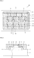
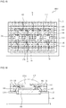
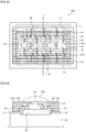
FIG. 1 is a plan view of alamp unit 100 in accordance with one embodiment, andFIG. 2 is a cross-sectional view of thelamp unit 100 shown inFIG. 1 taken along the line A-B. - With reference to
FIGs. 1 and 2 , thelamp unit 100 includes afirst substrate 101, asecond substrate 102, pluralconductive layers devices 130, aprotecting layer 140, awavelength conversion layer 150, andplural wires - The
second substrate 102 may be disposed on thefirst substrate 101, and the area of thesecond substrate 102 may be smaller than the area of thefirst substrate 101. In accordance with another embodiment, the area of thesecond substrate 102 may be equal to the area of thefirst substrate 101. - The
first substrate 101 may be a substrate having first thermal conductivity, thesecond substrate 102 may be a substrate having second thermal conductivity, and the first thermal conductivity may be greater than the second thermal conductivity. This serves to rapidly dissipate heat generated from light emittingdevice 130 disposed on thesecond substrate 102 to the outside through thefirst substrate 101. - The
first substrate 101 may be a metal substrate, for example, a metal core printed circuit board (MCPCB). Thefirst substrate 101 is a heat dissipation plate having high thermal conductivity, and may be formed of one selected from the group consisting of copper (Cu), aluminum (Al), silver (Ag), and gold (Au), or an alloy thereof. - The
second substrate 102 may be an insulating substrate, for example, a ceramic substrate having high thermal conductivity. Thesecond substrate 102 may be formed of a nitride, for example, AIN. Otherwise, thesecond substrate 102 may include an anodized layer. - The
first substrate 101 and thesecond substrate 102 may be formed in various shapes. - In accordance with one embodiment, the
first substrate 101 may be provided with acavity 105 formed in a designated region thereof, and thesecond substrate 102 may be disposed within thecavity 105 of thefirst substrate 101. Here, thefirst substrate 101 may include at least one of Al, Cu, and Au, and thesecond substrate 102 may include AIN. - In accordance with another embodiment, the
first substrate 101 and thesecond substrate 102 may be sequentially laminated to form a laminated structure. Here, thefirst substrate 101 may include at least one of Al, Cu, and Au, and thesecond substrate 102 may include an anodized layer. - In accordance with another embodiment, the
first substrate 101 and thesecond substrate 102 may be formed of the same material. Here, thefirst substrate 101 and thesecond substrate 102 may include at least one of AIN, Al, Cu, and Au. - The upper surface of the
second substrate 102 on which thelight emitting devices 130 are disposed may be formed as a flat surface or a curved surface, such as a concave surface or a convex surface. Otherwise, the upper surface of thesecond substrate 102 may be formed in a shape in which at least two of a concave surface, a convex surface, and a flat surface are combined. - The third
conductive layer 112 and the fourthconductive layer 114 may be disposed on thefirst substrate 101 such that they are separated from each other. Thefirst substrate 101 may include a first circuit pattern including the thirdconductive layer 112 and the fourthconductive layer 114. The thirdconductive layer 112 and the fourthconductive layer 114 are not limited to the shape shown inFIG. 1 and may have a variety of shapes. - The first
conductive layer 122 and the secondconductive layer 124 may be disposed on thesecond substrate 102 such that they are separated from each other. Thesecond substrate 102 may include a second circuit pattern including the firstconductive layer 122 and the secondconductive layer 124. - The
light emitting devices 130 are disposed on thesecond substrate 102. Plurallight emitting devices 130 are provided. The plurallight emitting devices 130 may be disposed on thesecond substrate 102 such that they are separated from one another. -
Conductive layer 124 may be plural in number and separated from one another. However, the disclosure is not limited thereto, and only one connected conductive layer may be formed. - Although
FIG. 1 illustrates one firstconductive layer 122, the disclosure is not limited thereto, and plural first conductive layers separated from one another may be disposed andwires 166 may be bonded to the respective first conductive layers. -
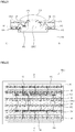
FIG. 28 is a view illustrating one embodiment of thelight emitting device 130 shown inFIG. 1 . - With reference to
FIG. 28 , thelight emitting device 130 includes asecond electrode 405, aprotective layer 440, acurrent blocking layer 445, alight emitting structure 450, apassivation layer 465, and afirst electrode 470. - For example, the
light emitting device 130 may be formed as a light emitting diode chip. - The
second electrode 405 together with thefirst electrode 470 provides power to thelight emitting structure 450. Thesecond electrode 405 may include asupport layer 410, abonding layer 415, abarrier layer 420, areflective layer 425, and anohmic layer 430. - The
support layer 410 supports thelight emitting structure 450. Thesupport layer 410 may be formed of a metal or a semiconductor material. Further, thesupport layer 410 may be formed of a material having high electrical conductivity and high thermal conductivity. For example, thesupport layer 410 may be formed of a metal material including at least one selected from the group consisting of copper (Cu), a Cu alloy, gold (Au), nickel (Ni), molybdenum (Mo), and copper-tungsten (Cu-W), or a semiconductor including at least one selected from the group consisting of Si, Ge, GaAs, ZnO, and SiC. - The
bonding layer 415 may be disposed between thesupport layer 410 and thebarrier layer 420 and serve to bond thesupport layer 410 and thebarrier layer 420. Thebonding layer 415 may include at least one selected from the group consisting of metals, for example, In, Sn, Ag, Nb, Pd, Ni, Au, and Cu. Since thebonding layer 415 serves to form thesupport layer 410 through a bonding method, if thesupport layer 410 is formed through a plating or deposition method, thebonding layer 415 may be omitted. - The
barrier layer 420 may be disposed under thereflective layer 425, theohmic layer 430, and theprotective layer 440, and prevent metal ions of thebonding layer 415 and thesupport layer 410 from diffusing into thelight emitting structure 450 via thereflective layer 425 and theohmic layer 430. For example, thebarrier layer 420 may include at least one selected from the group consisting of Ni, Pt, Ti, W, V, Fe, and Mo, and be formed in a monolayer or multilayer structure. - The
reflective layer 425 may be disposed on thebarrier layer 420. Thereflective layer 425 may reflect light incident from thelight emitting structure 450, and thus improve light extraction efficiency. Thereflective layer 425 may be formed of a light reflecting material, for example, at least one metal selected from the group consisting of Ag, Ni, Al, Rh, Pd, Ir, Ru, Mg, Zn, Pt, Au, and Hf, or an alloy thereof. - The
reflective layer 425 may be formed in a multilayer structure using a metal or an alloy and a light-transmitting conductive material, such as IZO, IZTO, IAZO, IGZO, IGTO, AZO, or ATO. For example, thereflective layer 425 may be formed of IZO/Ni, AZO/Ag, IZO/Ag/Ni, or AZO/Ag/Ni. - The
ohmic layer 430 may be disposed between thereflective layer 425 and thesecond semiconductor layer 452, and come into ohmic contact with thesecond semiconductor layer 452 so as to effectively provide power to thelight emitting structure 450. - The
ohmic layer 430 may be formed by selectively using a light-transmitting conductive layer and a metal. For example, theohmic layer 430 may be formed of a metal coming into ohmic contact with thesecond semiconductor layer 452, for example, at least one selected from the group consisting of Ag, Ni, Cr, Ti, Pd, Ir, Sn, Ru, Pt, Au, and Hf. - The
protective layer 440 may be disposed on the edge region of thesecond electrode layer 405. For example, theprotective layer 440 may be disposed on the edge region of theohmic layer 430, the edge region of thereflective layer 425, the edge region of thebarrier layer 420, or the edge region of thesupport layer 410. - The
protective layer 440 may prevent lowering of reliability of thelight emitting device 130 due to debonding at the interface between thelight emitting structure 450 and thesecond electrode layer 405. Theprotective layer 440 may be formed of an electrically insulating material, for example, ZnO, SiO2, Si3N4, TiOx (x being a positive real number), or Al2O3. - The
current blocking layer 445 may be disposed between theohmic layer 430 and thelight emitting structure 450. The upper surface of thecurrent blocking layer 445 may contact thesecond semiconductor layer 452, and the lower surface or the lower and side surfaces of thecurrent blocking layer 445 may contact theohmic layer 430. Thecurrent blocking layer 445 may be disposed so as to at least partially overlap with thefirst electrode 470 in the vertical direction. - The
current blocking layer 445 may be formed between theohmic layer 430 and thesecond semiconductor layer 452 or formed between thereflective layer 425 and theohmic layer 430, but the disclosure is not limited thereto. - The
light emitting structure 450 may be disposed on theohmic layer 430 and theprotective layer 440. The side surface of thelight emitting structure 450 may be inclined during an isolation etching process for dividing thelight emitting structure 450 into unit chips. Thelight emitting structure 450 may include thesecond semiconductor layer 452, anactive layer 454, and afirst semiconductor layer 456, and generate light. - The
second semiconductor layer 452 may be formed of a group III-V or II-VI compound semiconductor, and be doped with a second conductivity-type dopant. For example, the second semiconductor layer 451 may be formed of a semiconductor having a composition formula of InxAlyGa1-x-yN (0≤x≤1, 0≤y≤1, 0≤x+y≤1), and be doped with a P-type dopant (for example, Mg, Zn, Ca, Sr, or Ba). - The
active layer 454 may generate light by energy released through recombination of electrons and holes provided from thefirst semiconductor layer 456 and thesecond semiconductor layer 452. - The
active layer 454 may be formed of a semiconductor compound, for example, a group III-V or II-VI compound semiconductor, and be formed in a single well structure, a multi-well structure, a quantum-wire structure, or a quantum dot structure. If theactive layer 454 is formed in a quantum well structure, theactive layer 454 may have a single or multi-quantum well structure having a well layer having a composition formula of InxAlyGa1-x-yN (0≤x≤1, 0≤y≤1, 0≤x+y≤1) and a barrier layer having a composition formula of InaAlbGa1-a-bN (0≤a≤1, 0≤b≤1, 0≤a+b≤1). The well layer may be formed of a material having an energy bandgap lower than the energy bandgap of the barrier layer. - The
first semiconductor layer 456 may be formed of a group III-V or II-VI compound semiconductor, and be doped with a first conductivity-type dopant. For example, thefirst semiconductor layer 456 may be formed of a semiconductor having a composition formula of InxAlyGa1-x-yN (0≤x≤1, 0≤y≤1, 0≤x+y≤1), and be doped with an N-type dopant (for example, Si, Ge, Sn, Se, or Te). - The
light emitting device 130 may emit one of blue light, red light, green light, and yellow light according to the compositions of thefirst semiconductor layer 456, theactive layer 454, and thesecond semiconductor layer 452 of thelight emitting structure 450. - The
passivation layer 465 may be disposed on the side surface of thelight emitting structure 450 so as to electrically protect thelight emitting structure 450. Thepassivation layer 465 may be disposed on a portion of the upper surface of the first semiconductor layer 455 or the upper surface of theprotective layer 440. Thepassivation layer 465 may be formed of an insulating material, for example, SiO2, SiOx, SiOxNy, Si3N4, or Al2O3. - The
first electrode 470 may be disposed on thefirst semiconductor layer 456. Thefirst electrode 470 may be formed in a designated pattern. Thefirst electrode 470 may include a pad part for wire-bonding, and branched finger electrodes (not shown) extending from the pad part. - In order to increase light extraction efficiency, a roughness pattern (not shown) may be formed on the upper surface of the
first semiconductor layer 456. Further, in order to increase light extraction efficiency, a roughness pattern (not shown) may be also formed on the upper surface of thefirst electrode 470. - The
light emitting device 130 may be electrically connected to the firstconductive layer 122 and the secondconductive layer 124. - The
second electrode 405 of thelight emitting device 130 may be bonded to the secondconductive layer 124 disposed on thesecond substrate 102 by eutectic bonding or die bonding, and be thus electrically connected to the secondconductive layer 124. - The
wires 166 is electrically connect thefirst electrodes 470 of thelight emitting devices 130 to the firstconductive layer 122 disposed on thesecond substrate 102. - The
wires 162 may electrically connect the firstconductive layer 122 disposed on thesecond substrate 102 to the thirdconductive layer 112 disposed on thefirst substrate 101. The number of thewires 162 may be 1 or more. - The
wires 164 may electrically connect the secondconductive layer 124 disposed on thesecond substrate 102 to the fourthconductive layer 114 disposed on thefirst substrate 101. The number of thewires 164 may be 1 or more. - The
wavelength conversion layer 150 is located on thelight emitting devices 130, and is adapted to convert the wavelength of light generated from thelight emitting devices 130. Thewavelength conversion layer 150 may include a colorless and transparent polymer resin, such as epoxy or silicon, and phosphors. Thewavelength conversion layer 150 may include at least one of a red phosphor, a green phosphor, and a yellow phosphor. Thewavelength conversion layer 150 surrounds at least a part of thewires 166. - The protecting
layer 140 may be disposed on thefirst substrate 101 and thesecond substrate 102 so as to surround thelight emitting devices 130 and thewires 162 to 166. The protectinglayer 140 may fill thecavity 105 of thefirst substrate 101. The upper surface of theprotecting layer 140 may be located at a position higher than the highest point of thewires 166. - The protecting
layer 140 may surround thewires 162 to 166, and prevent thewires 162 to 166 from being exposed to the outside or protruding to the outside. In this embodiment, the protectinglayer 140 may prevent the wires (for example, the wires 166) from being broken or damaged due to impact or pressure or corroding due to air, and thus prevent breakage or malfunction of thelight emitting devices 130. - The protecting
layer 140 may be formed of a non-conductive molding member which may reflect light, for example, white silicon, but the disclosure is not limited thereto. - Since the
protecting layer 140 closely contacts thelight emitting devices 130 and directly reflects light irradiated by thelight emitting devices 130, thelamp unit 100 in accordance with this embodiment may reduce light loss caused by absorption or transmission of light by air or thefirst substrate 101 and thesecond substrate 102, and improve light emission efficiency. -
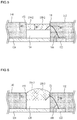
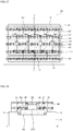
FIG. 3 is an enlarged view illustrating awavelength conversion layer 150 and awire 166 in accordance with one embodiment not forming part of the invention as claimed. - With reference to
FIG. 3 , the protectinglayer 140 may contact aside surface 152 of thewavelength conversion layer 150 and the side surface of thelight emitting device 130, and surround theside surface 152 of thewavelength conversion layer 150. - An
upper surface 154 of thewavelength conversion layer 150 may be flat, and be exposed from the protectinglayer 140. - The
upper surface 154 of thewavelength conversion layer 150 may be coplanar with anupper surface 142 of theprotecting layer 140. A height H2 from the upper surface of thelight emitting device 130 to theupper surface 154 of thewavelength conversion layer 150 may be equal to a height H3 from the upper surface of thelight emitting device 130 to theupper surface 142 of the protecting layer 140 (H2=H3). - In order to protect the
wire 166, theupper surface 154 of thewavelength conversion layer 150 and theupper surface 142 of theprotecting layer 140 may be located at a position higher than the highest point T1 of thewire 166. - The height H2 from the upper surface of the
light emitting device 130 to theupper surface 154 of thewavelength conversion layer 150 and theupper surface 142 of theprotecting layer 140 may exceed at least 50 µm. The reason for this is that the lowest height H1 of the highest point T1 of thewire 166 which may be formed by a manufacturing process is about 50 µm. Therefore, if the height from the upper surface of thelight emitting device 130 to theupper surface 154 of thewavelength conversion layer 150 and theupper surface 142 of theprotecting layer 140 is less than 50 µm, thewire 166 may be exposed from the protectinglayer 140. - The height H2 from the upper surface of the
light emitting device 130 to theupper surface 154 of thewavelength conversion layer 150 may be greater than a height H1 from the upper surface of thelight emitting device 130 to the highest point T1 of the wire 166 (H2>H1). This serves to prevent exposure of thewire 166. -
FIG. 4 is an enlarged view illustrating a wavelength conversion layer 150-1 and awire 166 in accordance with embodiment forming part of the invention as claimed. With reference toFIG. 4 , an upper surface 154-1 of the wavelength conversion layer 150-1 may be higher than theupper surface 142 of theprotecting layer 140. The upper surface 154-1 of the wavelength conversion layer 150-1 may protrude from theupper surface 142 of theprotecting layer 140. - A height H4 from the upper surface of the
light emitting device 130 to the upper surface 154-1 of the wavelength conversion layer 150-1 may be greater than the height H3 from the upper surface of thelight emitting device 130 to theupper surface 142 of the protecting layer 140 (H4>H3). -
FIG. 5 is an enlarged view illustrating a wavelength conversion layer 150-2 and awire 166 in accordance with another embodiment forming part of the invention as claimed. With reference toFIG. 5 , an upper surface 154-2 of the wavelength conversion layer 150-2 may be lower than theupper surface 142 of theprotecting layer 140. A height H5 from the upper surface of thelight emitting device 130 to the upper surface 154-2 of the wavelength conversion layer 150-2 may be lower than the height H3 from the upper surface of thelight emitting device 130 to theupper surface 142 of theprotecting layer 140 and be greater than the height H1 of the highest point T1 of the wire 166 (H1<H5<H3). -
FIG. 6 is an enlarged view illustrating a wavelength conversion layer 150-3 and awire 166 in accordance with another embodiment not forming part of the invention as claimed. With reference toFIG. 6 , an upper surface 154-3 of the wavelength conversion layer 150-3 may be curved. For example, the upper surface 154-3 of the wavelength conversion layer 150-3 may be formed in a dome shape or a hemispheric shape. Since the upper surface 154-3 of the wavelength conversion layer 150-3 is curved, in this embodiment, light irradiated from thelight emitting device 130 may be refracted and thus orientation angle of light may be improved. -
FIG. 7 is a view illustrating awavelength conversion layer 150 in accordance with one embodiment not forming part of the invention as claimed. With reference toFIG. 7 , thewavelength conversion layer 150 may correspond to regions S1 to S4 in which thelight emitting devices 130 are respectively located. Thewavelength conversion layer 150 may include plural portions (for example, 150-a, 150-b, 150-c, and 150-d) separated from one another, and these portions (for example, 150-a, 150-b, 150-c, and 150-d) may respectively correspond to thelight emitting devices 130. -
FIG. 8 is a view illustrating a wavelength conversion layer 150' in accordance with another embodiment not forming part of the invention as claimed. With reference toFIG. 8 , the wavelength conversion layer 150' may correspond to a region S5 formed by uniting regions in which thelight emitting devices 130 are respectively located and regions located between two neighboring light emittingdevices 130, and be formed in one body. -
FIG. 9 is a cross-sectional view of a lamp unit 100-1 in accordance with another embodiment not forming part of the invention as claimed. Elements in this embodiment which are substantially the same as those in the embodiment shown inFIG. 2 are denoted by the same reference numerals even though they are depicted in different drawings, and a detailed description thereof will thus be briefly given or omitted because it is considered to be unnecessary. - With reference to
FIG. 9 , the lamp unit 100-1 in accordance with this embodiment differs from thelamp unit 100 in accordance with the embodiment shown inFIG. 2 in that the lamp unit 100-1 includes a light-transmitting protecting layer 140-1. - That is, the protecting layer 140-1 may be formed of a non-conductive molding member which may transmit light. For example, the protecting layer 140-1 may be formed of silicon resin, epoxy resin, glass, glass ceramic, polyester resin, acrylic resin, urethane resin, nylon resin, polyamide resin, polyimide resin, vinyl chloride resin, polycarbonate resin, polyethylene resin, Teflon resin, polystyrene resin, polypropylene resin, or polyolefin resin.
- The protecting layer 140-1 shown in
FIG. 9 is the same as the protectinglayer 140 in the embodiment shown inFIG. 2 except for the material of the protecting layer 140-1. -
FIG. 10 is a plan view of a lamp unit 100-2 in accordance with another embodiment not forming part of the invention as claimed, andFIG. 11 is a cross-sectional view of the lamp unit 100-2 shown inFIG. 10 taken along the line A-B. Elements in this embodiment which are substantially the same as those in the embodiment shown inFIG. 2 are denoted by the same reference numerals even though they are depicted in different drawings, and a detailed description thereof will thus be briefly given or omitted because it is considered to be unnecessary. - With reference to
FIGs. 10 and11 , the lamp unit 100-2 further includeslenses 210, in addition to thelamp unit 100 in accordance with the embodiment shown inFIG. 2 . - The
lenses 210 may be disposed on thewavelength conversion layer 150 and theprotecting layer 140 so as to respectively correspond to thelight emitting devices 130. Thelenses 210 may refract light irradiated by the corresponding light emittingdevices 130, and adjust a light path of the lamp unit 100-2. - Although
FIG. 10 illustrates thelenses 210 as corresponding to the respectivelight emitting devices 130, one lens covering all the light emittingdevices 130 may be provided. -
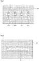
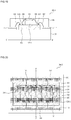
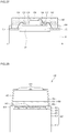
FIG. 12 is a plan view of a lamp unit 100-3 in accordance with another embodiment not forming part of the invention as claimed, andFIG. 13 is a cross-sectional view of the lamp unit 100-3 shown inFIG. 12 taken along the line A-B. Elements in this embodiment which are substantially the same as those in the embodiment shown inFIG. 2 are denoted by the same reference numerals even though they are depicted in different drawings, and a detailed description thereof will thus be briefly given or omitted because it is considered to be unnecessary. - With reference to
FIGs. 12 and13 , the lamp unit 100-3 includes afirst substrate 101, asecond substrate 102, pluralconductive layers protecting layer 140, and plural wires, 162, 164, and 166. - With reference to
FIGs. 12 and13 , while thelamp unit 100 in the embodiment shown inFIG. 2 includes the chip-typelight emitting devices 130 and thewavelength conversion layer 150 located on thelight emitting devices 130, the lamp unit 100-3 includes the light emitting devices 130-1, each of which is formed into one chip including thelight emitting device 130 and thewavelength conversion unit 150 of thelamp unit 100 in the embodiment shown inFIG. 2 . - For example, the
light emitting devices 130 may emit one of blue light, green light, red light, and yellow light, and the light emitting devices 130-1 may emit white light. -
FIG. 29 is a view illustrating one embodiment of the light emitting device 130-1 shown inFIG. 13 . Elements in this embodiment which are substantially the same as those in the embodiment shown inFIG. 28 are denoted by the same reference numerals even though they are depicted in different drawings, and a detailed description thereof will thus be briefly given or omitted because it is considered to be unnecessary. - With reference to
FIG. 29 , the light emitting device 130-1 further includes awavelength conversion layer 480. - The
wavelength conversion layer 480 may be disposed on thefirst semiconductor layer 456, and expose thefirst electrode 470. - For example, the
wavelength conversion layer 480 may be formed of a mixture of a colorless and transparent polymer resin, such as epoxy or silicon, and phosphors. Thewavelength conversion layer 480 may be formed by conformal coating of thefirst semiconductor layer 456 with the mixture of polymer resin and phosphors. In order to perform wire-bonding, thewavelength conversion layer 480 may expose a pad part (not shown) of thefirst electrode 470. - The upper surface of the
protecting layer 140 may be located at a position higher than the highest point of thewires 166 bonded to the firstconductive layer 122 disposed on thesecond substrate 102. The protectinglayer 140 may surround thewires 162 to 166, and prevent thewires 162 to 166 from being exposed to the outside or protruding to the outside. - The protecting
layer 140 may contact the side surface of the light emitting device 130-1, and the upper surface of the light emitting device 130-1 may be exposed from the protectinglayer 140. - In an embodiment not forming part of the invention as claimed the upper surface of the
protecting layer 140 may be coplanar with the upper surface of the light emitting device 130-1. That is, the height of the upper surface of the light emitting device 130-1 may be the same as the upper surface of theprotecting layer 140. Here, the upper surface of the light emitting device 130-1 may be the upper surface of thewavelength conversion layer 480. -
FIG. 14 is a cross-sectional view of a lamp unit 100-4 in accordance with another embodiment not forming part of the invention as claimed. Elements in this embodiment which are substantially the same as those in the embodiment shown inFIG. 13 are denoted by the same reference numerals even though they are depicted in different drawings, and a detailed description thereof will thus be briefly given or omitted because it is considered to be unnecessary. - With reference to
FIG. 14 , the lamp unit 100-4 differs from the lamp unit 100-3 in the embodiment shown inFIG. 13 in that the lamp unit 100-4 includes a protecting layer 140-1 formed of a light-transmitting molding member. The protecting layer 140-1 shown inFIG. 14 may be the same as the above-describedprotecting layer 140 except for the material of the protecting layer 140-1. -
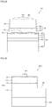
FIG. 15 is a plan view of a lamp unit 100-5 in accordance with another embodiment not forming part of the invention as claimed, andFIG. 16 is a cross-sectional view of the lamp unit 100-5 shown inFIG. 15 taken along the line A-B. - With reference to
FIGs. 15 and 16 , the lamp unit 100-5 further includeslenses 210, in addition to the lamp unit 100-3 in accordance with the embodiment shown inFIG. 13 . - The
lenses 210 may be disposed on theprotecting layer 140 so as to respectively correspond to the light emitting devices 130-1. Thelenses 210 may refract light irradiated by the corresponding light emitting devices 130-1, and adjust a light path of the lamp unit 100-5. - Although
FIG. 15 illustrates thelenses 210 as corresponding to the respective light emitting devices 130-1, one lens covering all the light emitting devices 130-1 may be provided. -
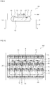
FIG. 17 is a plan view of alamp unit 200 in accordance with another embodiment not forming part of the invention as claimed, andFIG. 18 is a cross-sectional view of thelamp unit 200 shown inFIG. 17 taken along the line C-D. Elements in this embodiment which are substantially the same as those in the embodiment shown inFIGs. 1 and 2 are denoted by the same reference numerals even though they are depicted in different drawings, and a detailed description thereof will thus be briefly given or omitted because it is considered to be unnecessary. - With reference to
FIGs. 17 and 18 , thelamp unit 200, includes afirst substrate 101, asecond substrate 102, pluralconductive layers protecting layer 140, awavelength conversion layer 150, andplural wires - The
lamp unit 200 differs from thelamp unit 100 in the embodiment shown inFIG. 2 in that the light emitting devices 130-2 are lateral light emitting diodes, and the light emitting devices 130-2 are electrically connected to theconductive layers - The light emitting devices 130-2 may be disposed on the
second substrate 102. -
FIG. 30 is a view illustrating one embodiment of the light emitting device 130-2 shown inFIG. 18 . - With reference to
FIG. 30 , the light emitting device 130-2 includes asubstrate 310, a light emitting structure 320, aconductive layer 330, afirst electrode 342, and asecond electrode 344. - The
substrate 310 may be formed of a material proper for semiconductor material growth, i.e., a carrier wafer. Further, thesubstrate 310 may be formed of a material having high thermal conductivity, and be a conductive substrate or an insulating substrate. For example, thesubstrate 310 may be formed of a material including at least one of sapphire (Al2O3), GaN, SiC, ZnO, Si, GaP, InP, Ga2O3, and GaAs. A concave-convex pattern may be formed on the upper surface of thesubstrate 310. - Further, a layer or a pattern using a compound semiconductor of group II to VI atoms, for example, at least one of a ZnO layer (not shown), a buffer layer (not shown), and an undoped semiconductor layer (not shown), may be formed on the
substrate 310. The buffer layer or the undoped semiconductor layer may be formed using a compound semiconductor of group III-V atoms, the buffer layer may reduce a difference of lattice constants with thesubstrate 310, and the undoped semiconductor layer may be formed of an undoped GaN-based semiconductor. - The
light emitting structure 450 may be a semiconductor layer generating light, and include afirst semiconductor layer 456, anactive layer 454, and asecond semiconductor layer 452. Thefirst semiconductor layer 456, theactive layer 454, and thesecond semiconductor layer 452 may be the same as those in the embodiment shown inFIG. 28 . The light emitting devices 130-2 may emit one of blue light, green light, red light, and yellow light. - In the
light emitting structure 450, a portion of thesemiconductor layer 456 may be exposed by removing thesecond semiconductor layer 452, theactive layer 454 and the other portion of thesemiconductor layer 456. - The
conductive layer 330 reduces total reflection and has high light transmittance, and may thus increase extraction efficiency of light emitted from theactive layer 454 to thesecond semiconductor layer 452. - The
conductive layer 330 may be formed in a monolayer or multilayer structure using a transparent conductive oxide, for example, at least one selected from the group consisting of Indium Tin Oxide (ITO), Tin Oxide (TO), Indium Zinc Oxide (IZO), Indium Tin Zinc Oxide (ITZO), Indium Aluminum Zinc Oxide (IAZO), Indium Gallium Zinc Oxide (IGZO), Indium Gallium Tin Oxide (IGTO), Aluminum Zinc Oxide (AZO), Antimony Tin Oxide (ATO), Gallium Zinc Oxide (GZO), IrOx, RuOx, RuOx/ITO, Ni, Ag, Ni/IrOx/Au, and Ni/IrOx/Au/ITO. - The
first electrode 342 may be disposed on the exposedfirst semiconductor layer 456, and thesecond electrode 344 may be disposed on theconductive layer 330. - The first
conductive layer 122 and the second conductive layer 124-1 may be located on thesecond substrate 102 so as to be separated from each other, and the light emitting device 130-2 may be electrically connected to the firstconductive layer 122 and the second conductive layer 124-1. - The
substrate 310 of the light emitting device 130-2 may be bonded to thesecond substrate 102. - The
wire 166 may electrically connect thefirst electrode 342 of the light emitting device 130-2 to the firstconductive layer 122 disposed on thesecond substrate 102. Thewire 168 may electrically connect the second electrode 144 of the light emitting device 130-2 to the second conductive layer 124-1 disposed on thesecond substrate 102. - In order to protect the
wires wavelength conversion layer 150 and the upper surface of theprotecting layer 140 may be located at a position higher than the highest point T1 of each of thewires -
FIG. 19 is a cross-sectional view of a lamp unit 200-1 in accordance with another embodiment not forming part of the invention as claimed. Elements in this embodiment which are substantially the same as those in the embodiment shown inFIG. 18 are denoted by the same reference numerals even though they are depicted in different drawings, and a detailed description thereof will thus be briefly given or omitted because it is considered to be unnecessary. - With reference to
FIG. 19 , the lamp unit 200-1 differs from thelamp unit 200 in the embodiment shown inFIG. 18 in that the protecting layer 140-1 transmits light. -
FIG. 20 is a plan view of a lamp unit 200-2 in accordance with another embodiment not forming part of the invention as claimed, andFIG. 21 is a cross-sectional view of the lamp unit 200-2 shown inFIG. 20 taken along the line C-D. Elements in this embodiment which are substantially the same as those in the embodiment shown inFIG. 18 are denoted by the same reference numerals even though they are depicted in different drawings, and a detailed description thereof will thus be briefly given or omitted because it is considered to be unnecessary. - With reference to
FIGs. 20 and21 , the lamp unit 200-2 further includeslenses 210, in addition to thelamp unit 200 in accordance with the embodiment shown inFIG. 18 . Thelenses 210 may be disposed on thewavelength conversion layer 150 and theprotecting layer 140 so as to respectively correspond to the light emitting devices 130-2. Thelenses 210 may refract light irradiated by the corresponding light emitting devices 130-2, and adjust a light path of the lamp unit 200-2. -
FIG. 22 is a plan view of a lamp unit 200-3 in accordance with another embodiment not forming part of the invention as claimed, andFIG. 23 is a cross-sectional view of the lamp unit 200-3 shown inFIG. 22 taken along the line C-D. Elements in this embodiment which are substantially the same as those in the embodiment shown inFIGs. 17 and 18 are denoted by the same reference numerals even though they are depicted in different drawings, and a detailed description thereof will thus be briefly given or omitted because it is considered to be unnecessary. - With reference to
FIGs. 22 and23 , the lamp unit 200-3 includes afirst substrate 101, asecond substrate 102, pluralconductive layers protecting layer 140, and plural wires, 162, 164, 166, and 168. - With reference to
FIGs. 22 and23 , while thelamp unit 200 in the embodiment shown inFIG. 18 includes the chip-type light emitting devices 130-2 and thewavelength conversion layer 150 located on the light emitting devices 130-2, the lamp unit 200-3 includes the light emitting devices 130-3, each of which is formed into one chip including the light emitting device 130-2 and thewavelength conversion unit 150 of thelamp unit 200 in the embodiment shown inFIG. 18 . - For example, the light emitting devices 130-2 may emit one of blue light, green light, red light, and yellow light, and the light emitting devices 130-3 may emit white light.
-
FIG. 31 is a view illustrating one embodiment of the light emitting device 130-3 shown inFIG. 23 . Elements in this embodiment which are substantially the same as those in the embodiment shown inFIG. 30 are denoted by the same reference numerals even though they are depicted in different drawings, and a detailed description thereof will thus be briefly given or omitted because it is considered to be unnecessary. - With reference to
FIG. 31 , the light emitting device 130-3 further includes awavelength conversion layer 350. - The
wavelength conversion layer 350 may be disposed on thesecond semiconductor layer 452, and expose thesecond electrode 344. In an embodiment not forming part of the invention as claimed the upper surface of theprotecting layer 140 may be coplanar with the upper surface of the light emitting device 130-3. That is, the height of the upper surfaces of the light emitting device 130-3 may be the same as the upper surface of theprotecting layer 140. Here, the upper surface of the light emitting device 130-3 may be the upper surface of thewavelength conversion layer 350. - The protecting
layer 140 may contact the side surface of the light emitting device 130-3, and the upper surface of the light emitting device 130-3 may be exposed from the protectinglayer 140. - Since the height of the highest point of the
wires protecting layer 140, breakage of and damage to thewires -
FIG. 24 is a cross-sectional view of a lamp unit 200-4 in accordance with another embodiment not forming part of the invention as claimed. Elements in this embodiment which are substantially the same as those in the embodiment shown inFIG. 23 are denoted by the same reference numerals even though they are depicted in different drawings, and a detailed description thereof will thus be briefly given or omitted because it is considered to be unnecessary. - With reference to
FIG. 24 , while theprotecting layer 140 of the lamp unit 200-3 shown inFIG. 23 is a reflective member, a protecting layer 140-1 of the lamp unit 200-4 may transmit light. -
FIG. 25 is a plan view of a lamp unit 200-5 in accordance with another embodiment not forming part of the invention as claimed, andFIG. 26 is a cross-sectional view of the lamp unit 200-5 shown inFIG. 25 taken along the line C-D. - Elements in this embodiment which are substantially the same as those in the embodiment shown in
FIGs. 22 and23 are denoted by the same reference numerals even though they are depicted in different drawings, and a detailed description thereof will thus be briefly given or omitted because it is considered to be unnecessary. - With reference to
FIG. 25 and 26 , in order to refract light irradiated from the light emitting devices 130-3 and adjust a light path, the lamp unit 200-5 may further includelenses 210, in addition to the lamp unit 200-3 in accordance with the embodiment shown inFIG. 23 . -
FIG. 27 is a cross-sectional view of a lamp unit in accordance with another embodiment not forming part of the invention as claimed. The lamp unit in the embodiment shown inFIG. 27 is a modification of thelamp unit 100 shown inFIG. 1 , and may further include amolding fixation unit 190. - With reference to
FIG. 27 , themolding fixation unit 190 may be disposed on thefirst substrate 101 and the pluralconductive layers protecting layer 140, and support and fix the edge of theprotecting layer 140. - The
molding fixation unit 190 may be disposed on thefirst substrate 101 and the pluralconductive layers devices 150, and theprotecting layer 140 may be formed by discharging a molding member to the inside of themolding fixation unit 190 and hardening the discharged molding member. Here, themolding fixation unit 190 may prevent the discharged molding member from overflowing, and serve to support theprotecting layer 140 after hardening. - The shape of the
molding fixation unit 190 may be determined by the desired shape of theprotecting layer 140. For example, themolding fixation unit 190 may have a circular shape, an oval shape, and a polygonal shape, such as a rectangle, but the disclosure is not limited thereto. - The
molding fixation unit 190 may be additionally applied to the lamp units 100-2 to 100-5, 200, and 200-1 to 200-5 in accordance with other embodiments. -
FIG. 32 is a cross-sectional view of aheadlamp 800 for vehicles in accordance with one embodiment. - With reference to
FIG. 32 , theheadlamp 800 includes alamp unit 801, areflector 802, ashade 803, and alens 804. - The
lamp unit 801 may be one of the above-describedlamp units 100, 100-1 to 100-5, 200, and 200-1 to 200-5 in accordance with the embodiments, and generate light. - The
reflector 802 may reflect light irradiated by thelamp unit 801 in a designated direction. Theshade 803 may be disposed between thereflector 802 and thelens 804. Theshade 803 is a member which blocks or reflects a portion of light reflected by thereflector 802 and proceeding to thelens 804 to form a light distribution pattern desired by a designer. - Here, one side 803-1 of the
shade 803 adjacent to thelens 804 and the other side 803-2 of theshade 803 adjacent to thelamp unit 801 may have different heights. - Light irradiated by the
lamp unit 801 may be reflected by thereflector 802 and theshade 803, pass through thelens 804, and then proceed to the front region of a vehicle. Here, thelens 804 may refract light reflected by thereflector 802. -
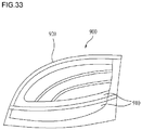
FIG. 33 is a view illustrating aheadlamp 900 for vehicles in accordance with another embodiment. - With reference to
FIG. 33 , theheadlamp 900 for vehicles may include alamp unit 910 and alight housing 920 - The
lamp unit 910 may include at least one of the above-describedlamp units 100, 100-1 to 100-5, 200, and 200-1 to 200-5 in accordance with the embodiments. - The
light housing 920 may accommodate thelamp unit 910, and be formed of a light-transmitting material. Thelight housing 920 for vehicles may be curved according to a region or design of a vehicle on which thelight housing 920 is mounted. - Each of the above-described
headlamps - As is apparent from the above description, a lamp unit in accordance with one embodiment may protect wires bonded to light emitting devices and reduce light loss.
- Although embodiments have been described with reference to a number of illustrative embodiments thereof, it should be understood that numerous other modifications and embodiments can be devised by those skilled in the art that will fall within the spirit and scope of the principles of this disclosure. More particularly, various variations and modifications are possible in the component parts and/or arrangements of the subject combination arrangement within the scope of the appended claims. In addition to variations and modifications in the component parts and/or arrangements, alternative uses will also be apparent to those skilled in the art.
Claims (14)
- A lamp unit (100) comprising:a first substrate (101);a second substrate (102) disposed on the first substrate (101);light emitting devices (130) disposed on the second substrate (102), wherein each of the light emitting devices (130) includes a light emitting structure (450) including a first semiconductor layer (456), an active layer (454), and a second semiconductor layer (452), and adapted to generate light in operation anda wavelength conversion layer (150) disposed on the light emitting structure (450) and adapted to convert the wavelength of light irradiated from the light emitting structure (450);a first conductive layer (122) and a second conductive layer (124) disposed on the second substrate (102);at least one wire (164, 166) electrically connecting at least one of the first conductive layer (122) and the second conductive layer (124) to each of the light emitting devices (130); anda protecting layer (140) disposed on the first substrate (101) and the second substrate (102) and surrounding the light emitting devices (130) and the at least one wire (164, 166) wherein an upper surface of the wavelength conversion layer (150) is exposed from the protecting layer (140), andwherein the upper surface of the protecting layer (140) is located at a position higher than the highest point of the at least one wire (166), characterised in that
the wavelength conversion layer (150) surrounds at least a part of the at least one wire (166), and wherein a height from an upper surface of the light emitting device (130) to the upper surface of the wavelength conversion layer (150) is different from a height from the upper surface of the light emitting device (130) to the upper surface of the protecting layer (140) and,wherein the upper surface of the protecting layer (140) is spaced away from an edge of the upper surface of the wavelength conversion layer (150). - The lamp unit (100) according to claim 1, wherein the protecting layer (140) is formed of a molding member reflecting light.
- The lamp unit 8100) according to claim 1, wherein the protecting layer (140) is formed of a light-transmitting molding member.
- The lamp unit (100) according to claim 1, wherein the protecting layer (140) contacts the side surfaces of the light emitting devices (130).
- The lamp unit (100) according to any one of claims 1 to 4, wherein the upper surfaces of the light emitting devices (130) are coplanar with the upper surface of the protecting layer (140).
- The lamp unit (100) according to any one of claims 1 to 5, wherein the upper surfaces of the light emitting devices (130) are exposed from the protecting layer (140).
- The lamp unit (100) according to any one of claims 1 to 6, wherein the first substrate (101) is provided with a cavity (105), the second substrate (102) is disposed within the cavity (105), and the protecting layer (140) fills the cavity (105).
- The lamp unit (100) according to any one of claims 1 to 7, further comprising:a third conductive layer (112) and a fourth conductive layer (114) disposed on the first substrate (101);first wires electrically connecting the first conductive layer (122) to the third conductive layer (112); andsecond wires electrically connecting the second conductive layer (124) to the fourth conductive layer (114),wherein the protecting layer (140) surrounds the first wires and the second wires.
- The lamp unit (100) according to any one of claims 1 to 8, further comprising lenses (210) corresponding to the light emitting devices (130) and disposed on the protecting layer (140).
- The lamp unit (100) according to any one of claims 1 to 9, wherein the first substrate (101) is a metal core printed circuit board (MCPCB), and the second substrate (102) is a ceramic substrate.
- The lamp unit (100) according to claim 1, wherein the height from the upper surface of the light emitting device (130) to the upper surface of the wavelength conversion layer (150) is higher than the height from the upper surface of the light emitting device (130) to the upper surface of the protecting layer (140).
- The lamp unit (100) according to any one of claims 1 to 11, wherein the upper surface of the wavelength conversion layer (150) is located at a position higher than the highest point of the at least one wire (166).
- The lamp unit (100) according to any one of claims 1 to 12, wherein the protecting layer (140) contacts the side surfaces of the light emitting devices (130) and the side surface of the wavelength conversion layer (150).
- The lamp unit (100) according to claim 1, wherein the height from the upper surface of the light emitting device (130) to the upper surface of the wavelength conversion layer (150) is lower than the height from the upper surface of the light emitting device (130) to the upper surface of the protecting layer (140).
Applications Claiming Priority (1)
| Application Number | Priority Date | Filing Date | Title |
|---|---|---|---|
| KR1020130009672A KR20140096722A (en) | 2013-01-29 | 2013-01-29 | A lamp unit |
Publications (3)
| Publication Number | Publication Date |
|---|---|
| EP2760046A2 EP2760046A2 (en) | 2014-07-30 |
| EP2760046A3 EP2760046A3 (en) | 2016-01-13 |
| EP2760046B1 true EP2760046B1 (en) | 2019-06-12 |
Family
ID=48877163
Family Applications (1)
| Application Number | Title | Priority Date | Filing Date |
|---|---|---|---|
| EP13178747.5A Active EP2760046B1 (en) | 2013-01-29 | 2013-07-31 | Lamp unit |
Country Status (5)
| Country | Link |
|---|---|
| US (1) | US9190578B2 (en) |
| EP (1) | EP2760046B1 (en) |
| JP (1) | JP6228781B2 (en) |
| KR (1) | KR20140096722A (en) |
| CN (1) | CN103972219B (en) |
Families Citing this family (8)
| Publication number | Priority date | Publication date | Assignee | Title |
|---|---|---|---|---|
| US10217918B2 (en) | 2014-08-26 | 2019-02-26 | Lg Innotek Co., Ltd. | Light-emitting element package |
| JP6442981B2 (en) * | 2014-10-28 | 2018-12-26 | 株式会社村田製作所 | Coil parts |
| KR102344533B1 (en) * | 2015-02-12 | 2021-12-29 | 엘지이노텍 주식회사 | Lighting emitting device package |
| US10407567B2 (en) * | 2015-03-31 | 2019-09-10 | Dow Global Technologies Llc | Flooding compounds for telecommunication cables having polymeric filler and branched olefinic fluid |
| KR102608419B1 (en) * | 2016-07-12 | 2023-12-01 | 삼성디스플레이 주식회사 | Display Apparatus and Method for manufacturing the same |
| CN107946441A (en) | 2016-10-12 | 2018-04-20 | 亿光电子工业股份有限公司 | Light-emitting device and light-emitting diode encapsulation structure |
| US20190295914A1 (en) * | 2018-03-23 | 2019-09-26 | Advanced Semiconductor Engineering, Inc. | Semiconductor device package and a method of manufacturing the same |
| FR3105346B1 (en) * | 2019-12-19 | 2022-10-07 | Valeo Vision | LIGHT ASSEMBLY FOR LIGHTING AND/OR SIGNALING DEVICE FOR MOTOR VEHICLE |
Family Cites Families (15)
| Publication number | Priority date | Publication date | Assignee | Title |
|---|---|---|---|---|
| JP2004319530A (en) * | 2003-02-28 | 2004-11-11 | Sanyo Electric Co Ltd | Optical semiconductor device and its manufacturing process |
| DE102004021233A1 (en) * | 2004-04-30 | 2005-12-01 | Osram Opto Semiconductors Gmbh | LED array |
| GB0504379D0 (en) * | 2005-03-03 | 2005-04-06 | Melexis Nv | Low profile overmoulded semiconductor package with transparent lid |
| JP2006269986A (en) * | 2005-03-25 | 2006-10-05 | Matsushita Electric Ind Co Ltd | Light-emitting device |
| JP4915052B2 (en) * | 2005-04-01 | 2012-04-11 | パナソニック株式会社 | LED component and manufacturing method thereof |
| US7777412B2 (en) * | 2007-03-22 | 2010-08-17 | Avago Technologies Ecbu Ip (Singapore) Pte. Ltd. | Phosphor converted LED with improved uniformity and having lower phosphor requirements |
| JP2009076749A (en) * | 2007-09-21 | 2009-04-09 | Toyoda Gosei Co Ltd | Led apparatus, and method of manufacturing the same |
| JP4808244B2 (en) * | 2008-12-09 | 2011-11-02 | スタンレー電気株式会社 | Semiconductor light emitting device and manufacturing method thereof |
| JP5506313B2 (en) * | 2009-09-30 | 2014-05-28 | スタンレー電気株式会社 | Light emitting diode light source for vehicle headlight |
| KR101047721B1 (en) * | 2010-03-09 | 2011-07-08 | 엘지이노텍 주식회사 | Light emitting device, method for fabricating the light emitting device and light emitting device package |
| KR101064036B1 (en) * | 2010-06-01 | 2011-09-08 | 엘지이노텍 주식회사 | Light emitting device package and lighting system |
| JP5701523B2 (en) * | 2010-06-22 | 2015-04-15 | 日東電工株式会社 | Semiconductor light emitting device |
| DE102010024864B4 (en) * | 2010-06-24 | 2021-01-21 | OSRAM Opto Semiconductors Gesellschaft mit beschränkter Haftung | Optoelectronic semiconductor component |
| EP2447595B1 (en) * | 2010-10-27 | 2017-08-02 | LG Innotek Co., Ltd. | Light emitting module |
| CN106252491A (en) * | 2012-05-29 | 2016-12-21 | 晶元光电股份有限公司 | Light-emitting device |
-
2013
- 2013-01-29 KR KR1020130009672A patent/KR20140096722A/en not_active Application Discontinuation
- 2013-07-31 EP EP13178747.5A patent/EP2760046B1/en active Active
- 2013-08-05 JP JP2013162207A patent/JP6228781B2/en active Active
- 2013-08-06 US US13/960,319 patent/US9190578B2/en active Active
- 2013-09-09 CN CN201310406770.1A patent/CN103972219B/en active Active
Non-Patent Citations (1)
| Title |
|---|
| None * |
Also Published As
| Publication number | Publication date |
|---|---|
| US20140209947A1 (en) | 2014-07-31 |
| JP2014146783A (en) | 2014-08-14 |
| CN103972219A (en) | 2014-08-06 |
| US9190578B2 (en) | 2015-11-17 |
| JP6228781B2 (en) | 2017-11-08 |
| EP2760046A3 (en) | 2016-01-13 |
| EP2760046A2 (en) | 2014-07-30 |
| CN103972219B (en) | 2018-05-15 |
| KR20140096722A (en) | 2014-08-06 |
Similar Documents
| Publication | Publication Date | Title |
|---|---|---|
| US10651345B2 (en) | Light emitting device, light emitting device package including the device, and lighting apparatus including the package | |
| EP2760046B1 (en) | Lamp unit | |
| US11094850B2 (en) | Light emitting device and lighting apparatus having enhanced optical and electrical characteristics by diffusion barrier layer | |
| US8368100B2 (en) | Semiconductor light emitting diodes having reflective structures and methods of fabricating same | |
| KR102346643B1 (en) | Light emitting device, manufacturing method for light emittin device, and lighting module having the light emitting device | |
| US10892390B2 (en) | Light-emitting element and light-emitting element package including the same | |
| KR102407329B1 (en) | Light source module and lighting apparatus | |
| KR20120030761A (en) | A light emitting device package and a light emitting module | |
| KR20160109427A (en) | Light emitting device and light unit having thereof | |
| US20190086039A1 (en) | Light emitting device package and lighting apparatus including the same | |
| EP3343644B1 (en) | Light-emitting device and light-emitting device package comprising same | |
| KR20160032429A (en) | Light emitting device package | |
| KR20200134465A (en) | Light emitting device package, lighting device and method of manufacturing the same | |
| KR102251225B1 (en) | Light source module | |
| KR101679760B1 (en) | A light emitting device | |
| KR102412620B1 (en) | Light emitting device and lighting emitting apparatus having thereof | |
| US10593848B2 (en) | Light emitting device package and light emitting apparatus | |
| KR102509312B1 (en) | Light emitting device package | |
| KR102510591B1 (en) | Light emitting device and light emitting device package | |
| KR102426873B1 (en) | A light emitting device package | |
| KR101735672B1 (en) | A light emitting device and a light emitting device package | |
| KR101692508B1 (en) | A light emitting device | |
| KR20150142422A (en) | A light emitting device and a lamp unit including the same | |
| KR20150144190A (en) | A lamp unit |
Legal Events
| Date | Code | Title | Description |
|---|---|---|---|
| PUAI | Public reference made under article 153(3) epc to a published international application that has entered the european phase |
Free format text: ORIGINAL CODE: 0009012 |
|
| 17P | Request for examination filed |
Effective date: 20140331 |
|
| AK | Designated contracting states |
Kind code of ref document: A2 Designated state(s): AL AT BE BG CH CY CZ DE DK EE ES FI FR GB GR HR HU IE IS IT LI LT LU LV MC MK MT NL NO PL PT RO RS SE SI SK SM TR |
|
| AX | Request for extension of the european patent |
Extension state: BA ME |
|
| PUAL | Search report despatched |
Free format text: ORIGINAL CODE: 0009013 |
|
| AK | Designated contracting states |
Kind code of ref document: A3 Designated state(s): AL AT BE BG CH CY CZ DE DK EE ES FI FR GB GR HR HU IE IS IT LI LT LU LV MC MK MT NL NO PL PT RO RS SE SI SK SM TR |
|
| AX | Request for extension of the european patent |
Extension state: BA ME |
|
| RIC1 | Information provided on ipc code assigned before grant |
Ipc: H01L 33/54 20100101ALN20151207BHEP Ipc: H01L 25/075 20060101AFI20151207BHEP Ipc: H01L 33/50 20100101ALN20151207BHEP Ipc: H01L 33/62 20100101ALN20151207BHEP |
|
| STAA | Information on the status of an ep patent application or granted ep patent |
Free format text: STATUS: EXAMINATION IS IN PROGRESS |
|
| 17Q | First examination report despatched |
Effective date: 20161104 |
|
| RAP1 | Party data changed (applicant data changed or rights of an application transferred) |
Owner name: LG INNOTEK CO., LTD. |
|
| GRAP | Despatch of communication of intention to grant a patent |
Free format text: ORIGINAL CODE: EPIDOSNIGR1 |
|
| STAA | Information on the status of an ep patent application or granted ep patent |
Free format text: STATUS: GRANT OF PATENT IS INTENDED |
|
| RIC1 | Information provided on ipc code assigned before grant |
Ipc: H01L 33/62 20100101ALN20181129BHEP Ipc: H01L 33/50 20100101ALN20181129BHEP Ipc: H01L 33/54 20100101ALN20181129BHEP Ipc: H01L 25/075 20060101AFI20181129BHEP Ipc: H01L 33/56 20100101ALN20181129BHEP |
|
| INTG | Intention to grant announced |
Effective date: 20181219 |
|
| GRAS | Grant fee paid |
Free format text: ORIGINAL CODE: EPIDOSNIGR3 |
|
| GRAA | (expected) grant |
Free format text: ORIGINAL CODE: 0009210 |
|
| STAA | Information on the status of an ep patent application or granted ep patent |
Free format text: STATUS: THE PATENT HAS BEEN GRANTED |
|
| AK | Designated contracting states |
Kind code of ref document: B1 Designated state(s): AL AT BE BG CH CY CZ DE DK EE ES FI FR GB GR HR HU IE IS IT LI LT LU LV MC MK MT NL NO PL PT RO RS SE SI SK SM TR |
|
| REG | Reference to a national code |
Ref country code: GB Ref legal event code: FG4D |
|
| REG | Reference to a national code |
Ref country code: CH Ref legal event code: EP |
|
| REG | Reference to a national code |
Ref country code: AT Ref legal event code: REF Ref document number: 1143697 Country of ref document: AT Kind code of ref document: T Effective date: 20190615 |
|
| REG | Reference to a national code |
Ref country code: DE Ref legal event code: R096 Ref document number: 602013056433 Country of ref document: DE |
|
| REG | Reference to a national code |
Ref country code: IE Ref legal event code: FG4D |
|
| REG | Reference to a national code |
Ref country code: NL Ref legal event code: MP Effective date: 20190612 |
|
| REG | Reference to a national code |
Ref country code: LT Ref legal event code: MG4D |
|
| PG25 | Lapsed in a contracting state [announced via postgrant information from national office to epo] |
Ref country code: FI Free format text: LAPSE BECAUSE OF FAILURE TO SUBMIT A TRANSLATION OF THE DESCRIPTION OR TO PAY THE FEE WITHIN THE PRESCRIBED TIME-LIMIT Effective date: 20190612 Ref country code: NO Free format text: LAPSE BECAUSE OF FAILURE TO SUBMIT A TRANSLATION OF THE DESCRIPTION OR TO PAY THE FEE WITHIN THE PRESCRIBED TIME-LIMIT Effective date: 20190912 Ref country code: LT Free format text: LAPSE BECAUSE OF FAILURE TO SUBMIT A TRANSLATION OF THE DESCRIPTION OR TO PAY THE FEE WITHIN THE PRESCRIBED TIME-LIMIT Effective date: 20190612 Ref country code: HR Free format text: LAPSE BECAUSE OF FAILURE TO SUBMIT A TRANSLATION OF THE DESCRIPTION OR TO PAY THE FEE WITHIN THE PRESCRIBED TIME-LIMIT Effective date: 20190612 Ref country code: SE Free format text: LAPSE BECAUSE OF FAILURE TO SUBMIT A TRANSLATION OF THE DESCRIPTION OR TO PAY THE FEE WITHIN THE PRESCRIBED TIME-LIMIT Effective date: 20190612 Ref country code: AL Free format text: LAPSE BECAUSE OF FAILURE TO SUBMIT A TRANSLATION OF THE DESCRIPTION OR TO PAY THE FEE WITHIN THE PRESCRIBED TIME-LIMIT Effective date: 20190612 |
|
| PG25 | Lapsed in a contracting state [announced via postgrant information from national office to epo] |
Ref country code: LV Free format text: LAPSE BECAUSE OF FAILURE TO SUBMIT A TRANSLATION OF THE DESCRIPTION OR TO PAY THE FEE WITHIN THE PRESCRIBED TIME-LIMIT Effective date: 20190612 Ref country code: GR Free format text: LAPSE BECAUSE OF FAILURE TO SUBMIT A TRANSLATION OF THE DESCRIPTION OR TO PAY THE FEE WITHIN THE PRESCRIBED TIME-LIMIT Effective date: 20190913 Ref country code: RS Free format text: LAPSE BECAUSE OF FAILURE TO SUBMIT A TRANSLATION OF THE DESCRIPTION OR TO PAY THE FEE WITHIN THE PRESCRIBED TIME-LIMIT Effective date: 20190612 Ref country code: BG Free format text: LAPSE BECAUSE OF FAILURE TO SUBMIT A TRANSLATION OF THE DESCRIPTION OR TO PAY THE FEE WITHIN THE PRESCRIBED TIME-LIMIT Effective date: 20190912 |
|
| REG | Reference to a national code |
Ref country code: AT Ref legal event code: MK05 Ref document number: 1143697 Country of ref document: AT Kind code of ref document: T Effective date: 20190612 |
|
| PG25 | Lapsed in a contracting state [announced via postgrant information from national office to epo] |
Ref country code: RO Free format text: LAPSE BECAUSE OF FAILURE TO SUBMIT A TRANSLATION OF THE DESCRIPTION OR TO PAY THE FEE WITHIN THE PRESCRIBED TIME-LIMIT Effective date: 20190612 Ref country code: CZ Free format text: LAPSE BECAUSE OF FAILURE TO SUBMIT A TRANSLATION OF THE DESCRIPTION OR TO PAY THE FEE WITHIN THE PRESCRIBED TIME-LIMIT Effective date: 20190612 Ref country code: SK Free format text: LAPSE BECAUSE OF FAILURE TO SUBMIT A TRANSLATION OF THE DESCRIPTION OR TO PAY THE FEE WITHIN THE PRESCRIBED TIME-LIMIT Effective date: 20190612 Ref country code: PT Free format text: LAPSE BECAUSE OF FAILURE TO SUBMIT A TRANSLATION OF THE DESCRIPTION OR TO PAY THE FEE WITHIN THE PRESCRIBED TIME-LIMIT Effective date: 20191014 Ref country code: AT Free format text: LAPSE BECAUSE OF FAILURE TO SUBMIT A TRANSLATION OF THE DESCRIPTION OR TO PAY THE FEE WITHIN THE PRESCRIBED TIME-LIMIT Effective date: 20190612 Ref country code: NL Free format text: LAPSE BECAUSE OF FAILURE TO SUBMIT A TRANSLATION OF THE DESCRIPTION OR TO PAY THE FEE WITHIN THE PRESCRIBED TIME-LIMIT Effective date: 20190612 Ref country code: EE Free format text: LAPSE BECAUSE OF FAILURE TO SUBMIT A TRANSLATION OF THE DESCRIPTION OR TO PAY THE FEE WITHIN THE PRESCRIBED TIME-LIMIT Effective date: 20190612 |
|
| PG25 | Lapsed in a contracting state [announced via postgrant information from national office to epo] |
Ref country code: IT Free format text: LAPSE BECAUSE OF FAILURE TO SUBMIT A TRANSLATION OF THE DESCRIPTION OR TO PAY THE FEE WITHIN THE PRESCRIBED TIME-LIMIT Effective date: 20190612 Ref country code: SM Free format text: LAPSE BECAUSE OF FAILURE TO SUBMIT A TRANSLATION OF THE DESCRIPTION OR TO PAY THE FEE WITHIN THE PRESCRIBED TIME-LIMIT Effective date: 20190612 Ref country code: ES Free format text: LAPSE BECAUSE OF FAILURE TO SUBMIT A TRANSLATION OF THE DESCRIPTION OR TO PAY THE FEE WITHIN THE PRESCRIBED TIME-LIMIT Effective date: 20190612 Ref country code: IS Free format text: LAPSE BECAUSE OF FAILURE TO SUBMIT A TRANSLATION OF THE DESCRIPTION OR TO PAY THE FEE WITHIN THE PRESCRIBED TIME-LIMIT Effective date: 20191012 |
|
| REG | Reference to a national code |
Ref country code: CH Ref legal event code: PL |
|
| REG | Reference to a national code |
Ref country code: DE Ref legal event code: R097 Ref document number: 602013056433 Country of ref document: DE |
|
| PG25 | Lapsed in a contracting state [announced via postgrant information from national office to epo] |
Ref country code: MC Free format text: LAPSE BECAUSE OF FAILURE TO SUBMIT A TRANSLATION OF THE DESCRIPTION OR TO PAY THE FEE WITHIN THE PRESCRIBED TIME-LIMIT Effective date: 20190612 Ref country code: TR Free format text: LAPSE BECAUSE OF FAILURE TO SUBMIT A TRANSLATION OF THE DESCRIPTION OR TO PAY THE FEE WITHIN THE PRESCRIBED TIME-LIMIT Effective date: 20190612 |
|
| REG | Reference to a national code |
Ref country code: BE Ref legal event code: MM Effective date: 20190731 |
|
| PLBE | No opposition filed within time limit |
Free format text: ORIGINAL CODE: 0009261 |
|
| STAA | Information on the status of an ep patent application or granted ep patent |
Free format text: STATUS: NO OPPOSITION FILED WITHIN TIME LIMIT |
|
| PG25 | Lapsed in a contracting state [announced via postgrant information from national office to epo] |
Ref country code: DK Free format text: LAPSE BECAUSE OF FAILURE TO SUBMIT A TRANSLATION OF THE DESCRIPTION OR TO PAY THE FEE WITHIN THE PRESCRIBED TIME-LIMIT Effective date: 20190612 Ref country code: PL Free format text: LAPSE BECAUSE OF FAILURE TO SUBMIT A TRANSLATION OF THE DESCRIPTION OR TO PAY THE FEE WITHIN THE PRESCRIBED TIME-LIMIT Effective date: 20190612 |
|
| 26N | No opposition filed |
Effective date: 20200313 |
|
| PG25 | Lapsed in a contracting state [announced via postgrant information from national office to epo] |
Ref country code: CH Free format text: LAPSE BECAUSE OF NON-PAYMENT OF DUE FEES Effective date: 20190731 Ref country code: LU Free format text: LAPSE BECAUSE OF NON-PAYMENT OF DUE FEES Effective date: 20190731 Ref country code: BE Free format text: LAPSE BECAUSE OF NON-PAYMENT OF DUE FEES Effective date: 20190731 Ref country code: LI Free format text: LAPSE BECAUSE OF NON-PAYMENT OF DUE FEES Effective date: 20190731 Ref country code: SI Free format text: LAPSE BECAUSE OF FAILURE TO SUBMIT A TRANSLATION OF THE DESCRIPTION OR TO PAY THE FEE WITHIN THE PRESCRIBED TIME-LIMIT Effective date: 20190612 Ref country code: IS Free format text: LAPSE BECAUSE OF FAILURE TO SUBMIT A TRANSLATION OF THE DESCRIPTION OR TO PAY THE FEE WITHIN THE PRESCRIBED TIME-LIMIT Effective date: 20200224 |
|
| PG2D | Information on lapse in contracting state deleted |
Ref country code: IS |
|
| PG25 | Lapsed in a contracting state [announced via postgrant information from national office to epo] |
Ref country code: IE Free format text: LAPSE BECAUSE OF NON-PAYMENT OF DUE FEES Effective date: 20190731 Ref country code: FR Free format text: LAPSE BECAUSE OF NON-PAYMENT OF DUE FEES Effective date: 20190812 |
|
| GBPC | Gb: european patent ceased through non-payment of renewal fee |
Effective date: 20190912 |
|
| PG25 | Lapsed in a contracting state [announced via postgrant information from national office to epo] |
Ref country code: GB Free format text: LAPSE BECAUSE OF NON-PAYMENT OF DUE FEES Effective date: 20190912 |
|
| PG25 | Lapsed in a contracting state [announced via postgrant information from national office to epo] |
Ref country code: CY Free format text: LAPSE BECAUSE OF FAILURE TO SUBMIT A TRANSLATION OF THE DESCRIPTION OR TO PAY THE FEE WITHIN THE PRESCRIBED TIME-LIMIT Effective date: 20190612 |
|
| PG25 | Lapsed in a contracting state [announced via postgrant information from national office to epo] |
Ref country code: MT Free format text: LAPSE BECAUSE OF FAILURE TO SUBMIT A TRANSLATION OF THE DESCRIPTION OR TO PAY THE FEE WITHIN THE PRESCRIBED TIME-LIMIT Effective date: 20190612 Ref country code: HU Free format text: LAPSE BECAUSE OF FAILURE TO SUBMIT A TRANSLATION OF THE DESCRIPTION OR TO PAY THE FEE WITHIN THE PRESCRIBED TIME-LIMIT; INVALID AB INITIO Effective date: 20130731 |
|
| REG | Reference to a national code |
Ref country code: DE Ref legal event code: R081 Ref document number: 602013056433 Country of ref document: DE Owner name: SUZHOU LEKIN SEMICONDUCTOR CO. LTD., TAICANG, CN Free format text: FORMER OWNER: LG INNOTEK CO., LTD., SEOUL, KR |
|
| PG25 | Lapsed in a contracting state [announced via postgrant information from national office to epo] |
Ref country code: MK Free format text: LAPSE BECAUSE OF FAILURE TO SUBMIT A TRANSLATION OF THE DESCRIPTION OR TO PAY THE FEE WITHIN THE PRESCRIBED TIME-LIMIT Effective date: 20190612 |
|
| PGFP | Annual fee paid to national office [announced via postgrant information from national office to epo] |
Ref country code: DE Payment date: 20230607 Year of fee payment: 11 |