EP2357564A2 - Unité et méthode de commande de mémoire et support comportant un programme de réalisation - Google Patents
Unité et méthode de commande de mémoire et support comportant un programme de réalisation Download PDFInfo
- Publication number
- EP2357564A2 EP2357564A2 EP11156809A EP11156809A EP2357564A2 EP 2357564 A2 EP2357564 A2 EP 2357564A2 EP 11156809 A EP11156809 A EP 11156809A EP 11156809 A EP11156809 A EP 11156809A EP 2357564 A2 EP2357564 A2 EP 2357564A2
- Authority
- EP
- European Patent Office
- Prior art keywords
- bank
- access
- transfer
- memory
- data
- Prior art date
- Legal status (The legal status is an assumption and is not a legal conclusion. Google has not performed a legal analysis and makes no representation as to the accuracy of the status listed.)
- Withdrawn
Links
Images


Classifications
-
- G—PHYSICS
- G06—COMPUTING; CALCULATING OR COUNTING
- G06F—ELECTRIC DIGITAL DATA PROCESSING
- G06F13/00—Interconnection of, or transfer of information or other signals between, memories, input/output devices or central processing units
- G06F13/14—Handling requests for interconnection or transfer
- G06F13/16—Handling requests for interconnection or transfer for access to memory bus
- G06F13/1605—Handling requests for interconnection or transfer for access to memory bus based on arbitration
- G06F13/1647—Handling requests for interconnection or transfer for access to memory bus based on arbitration with interleaved bank access
-
- G—PHYSICS
- G11—INFORMATION STORAGE
- G11C—STATIC STORES
- G11C7/00—Arrangements for writing information into, or reading information out from, a digital store
- G11C7/10—Input/output [I/O] data interface arrangements, e.g. I/O data control circuits, I/O data buffers
- G11C7/1072—Input/output [I/O] data interface arrangements, e.g. I/O data control circuits, I/O data buffers for memories with random access ports synchronised on clock signal pulse trains, e.g. synchronous memories, self timed memories
-
- G—PHYSICS
- G11—INFORMATION STORAGE
- G11C—STATIC STORES
- G11C7/00—Arrangements for writing information into, or reading information out from, a digital store
- G11C7/22—Read-write [R-W] timing or clocking circuits; Read-write [R-W] control signal generators or management
Definitions
- the present invention relates to memory control units, memory control methods and media containing programs for realizing the same. More particularly, the present invention relates to a unit, a method and a medium containing a program, in a circuit controlling memory in which a delay develops depending on order of access thereto such as dynamic random access memory (DRAM) that transfers data in synchronization with an operation clock to be a basis of operation, i.e., synchronous DRAM (SDRAM), for optimizing the access order to increase an actual bus bandwidth to SDRAM.
- DRAM dynamic random access memory
- SDRAM synchronous DRAM
- SDRAM has been conventionally in existence as one of apparatus for storing data.
- burst transmission that continuously transfers data in synchronization with an operation clock can be designated, and the predetermined number of bits which is the smallest unit for read and write (hereinafter, referred to as a word length) can be continuously transferred the previously-specified number of times (hereinafter, referred to as a burst length) in one clock unit. Therefore, SDRAM has excellent usability.
- FIG. 27 shows a memory area of typical SDRAM.
- a memory area of SDRAM is generally divided into banks composed of a plurality of pages.
- SDRAM shown in FIG. 27 is divided into two banks, i.e., banks 0 and 1 which are each composed of "n" pages from a page 0 to a page (n-1).
- Each page is composed of "m” columns from a column 0 to a column (m-1).
- n and m are both integers of not less than 1. Since data is read and written column by column, the word length is equal to the number of bits in one column. For example, one column is 8 bits, m is 512, and n is 2048.
- FIG. 28 is a state-transition diagram of typical SDRAM.
- SDRAM generally comprises a "sense amplifier" in each bank.
- sense amplifier activate
- the memory area of SDRAM is divided into a plurality of banks, the decrease in actual transfer rates can be avoided by accessing different banks in the case of continuous access and performing precharge and activation processing in each bank during accessing the other bank.
- SDRAM is described in detail, for example, in "NEC DATASHEET, MOS Integrated Circuit ⁇ PD4516421A, 4516821A, and 45116161A for Rev.P 16M-bit Synchronous DRAM (Document number: M12939EJ3V0DS00 (3rd edition), Issue date: April 1998, N CK(K))" and "Japanese Patent Laying-Open No. 6-76567 : Semiconductor Memory Device and Synchronism Type Semiconductor Memory Device".
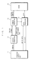
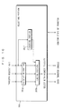
- FIG. 29 is a block diagram showing an example of a structure of a conventional memory control unit.
- the conventional memory control unit comprises a transfer-target unit 81, an address generator 82, a command generator 83, a data processor 84, and SDRAM 85.
- the transfer-target unit 81 outputs commands such as a start address, a transfer size, read/write and the like to the address generator 82 to transfer data between SDRAM 85.
- the address generator 82 generates a plurality of control signals for a start address, a burst length, read/write and the like based on the commands received from the transfer-target unit 81, and outputs the signals to the command generator 83.
- the command generator 83 generates control commands such as a clock (CLK), a row address strobe (RAS), a column address strobe (CAS), write enable (WE), addressing and the like based on the control signals received from the address generator 82, and thereby controls SDRAM 85 and the data processor 84.
- the data processor 84 transfers read data from SDRAM 85 to the transfer-target unit 81 according to the control commands received from the command generator 83, and also transfers write data from the transfer-target unit 81 to SDRAM 85.
- SDRAM 85 has features similar to those of typical SDRAM as described above, and is controlled by the control commands acquired from the command generator 83.
- FIG. 30 shows an example of a structure of a conventional memory system.
- the conventional memory system comprises transfer-target units 231 to 233, an arbiter 234, an SDRAM controller 235, and SDRAM 85.
- Each of the transfer-target units 231 to 233 outputs a transfer request signal to the arbiter 234 when required to transfer data with SDRAM 85, and outputs transfer information to the SDRAM controller 235 when a transfer enabling signal is returned from the arbiter 234.
- the arbiter 234 When acquiring a transfer request signal from any one of the transfer-target units, the arbiter 234 returns a transfer enabling signal to the transfer-target unit which outputs the transfer request signal.
- the arbiter 234 selects a higher-priority signal among the transfer request signals, then returns a transfer enabling signal to the transfer-target unit which outputs the selected transfer request signal. The same processing is performed to the remaining transfer request signals which are not selected.
- the SDRAM controller 235 is constituted by the address generator 82, the command generator 83, and the data processor 84 described in the above.
- the SDRAM controller 235 generates control commands such as CLK, RAS, CAS, WE, an access address and the like based on the transfer information from the transfer-target unit, and outputs the commands to SDRAM 85, thereby realizing data transfer between SDRAM 85 and the transfer-target unit which outputted the transfer information.
- SDRAM 85 has features similar to those of typical SDRAM described earlier, and is controlled by the control commands acquired from the SDRAM controller 235.
- precharge commands to the banks 0 and 1 are represented by “Pa” and “Pb” , respectively
- active commands to the banks 0 and 1 are represented by “Aa” and “Ab”, respectively
- read commands to the banks 0 and 1 are represented by “Ra” and “Rb”, respectively.
- CAS latency is "3" clocks, and a burst length is "8" data.
- an interval in which a precharge command, an active command, and a read command can be issued to the same bank that is an interval Pa ⁇ Aa ⁇ Ra, or an interval Pb ⁇ Ab ⁇ Rb
- an interval in which active commands are issued to the banks 0 and 1 that is an interval Aa ⁇ Ab
- the command generator 83 first issues the Pa command to the bank 0 including the data a1 and a2 to read the data (in the zeroth cycle). Since the Aa command can not be continuously issued to the bank 0 due to the constraint of the CAS latency, the Pb command is issued to the bank 1 in the interval (in the first cycle). Afterwards, the Aa command is issued at the third clock from the issue of the Pa command (in the third cycle).
- a command which can be issued next is the Ra command to the bank 0 or the Ab command to the bank 1, however, the both commands must wait until three clocks have elapsed because of the constraint of the CAS latency.
- the command generator 83 processes the control signals in the order that they are sent from the address generator 82. Accordingly, the command generator 83 issues the Ra command first after three clocks have elapsed (in the sixth cycle), and next issues the Ab command (in the seventh cycle).
- the Rb command resultantly, is issued in the tenth cycle at the earliest.
- the data a1 and a2 are sequentially read from the ninth cycle which is at the third clock from the issue of the Ra command, and data b1 to b8 are sequentially read from the thirteenth cycle which is at the third clock from the issue of the Rb command. Accordingly, entire data reading is terminated in the twentieth cycle.
- the conventional memory control unit thus, has the fixed rule and constraint as described above. Therefore, since the data in the banks 0 and 1 can not be continuously read (see the eleventh to twelfth cycles in FIG. 32 ), there occurs some cases that it takes much time to terminate the entire data reading. That is to say, when data is continuously transferred across the bank boundary from an arbitrary address in SDRAM 85, such problem arises as the efficiency in data transfer is degraded due to the uniquely-determined procedure of issuing commands.
- SDRAM can not be efficiently controlled in some cases.
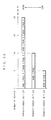
- FIG. 33 shows, column by column, numbers of pages including columns to be accessed in data transfer requested by transfer-target units, and numbers of banks to which the pages belong, in order that the columns are accessed.
- priority of data transfer becomes higher toward the upper transfer-target unit
- the transfer-target unit 231 requests for data transfer to alternatively access the page 0 in the bank 0 and the page 0 in the bank 1 four times in total in units of eight columns
- the transfer-target unit 232 requests for data transfer to access the page 1 in the bank 1 twice in total in units of eight columns
- the transfer-target unit 233 requests for data transfer to access the page 1 in the bank 0 only once in eight columns.
- FIG. 34 shows order of the data transfer in operation clocks in the case where the data transfer as shown in FIG. 33 is simultaneously requested from the transfer-target units.
- CAS latency is 3, and a burst length is 8 .
- the CAS latency here represents latency (the number of clocks) from input of a read command to reading of the corresponding data.
- the burst length here represents the number of words outputted or inputted in a read cycle or a write cycle. Since the CAS latency is 3 in the present example, read data until one clock after a precharge command is inputted is effective.
- an interval between a precharge command and an active command and an interval between an active command and a read command to the same bank must be both more than or equal to three clocks.
- data is transferred according to the priority, i.e., in order of the transfer-target unit 231, the transfer-target unit 232, and the transfer-target unit 233.
- a column to be transferred at the last in response to a request from the transfer-target unit 231 is included in the page 0 in the bank 1
- a column to be first transferred in response to a request from the transfer-target unit 232 is included in the page 1 in the bank 1. That is, the columns included in the different pages in the same bank are to be continuously accessed. Accordingly, since precharge and active processing can not be performed while accessing the other bank, overhead is produced in the interval, thereby decreasing actual transfer rates.
- SDRAM as described above is used as memory for temporarily storing decoded image data decoded by a video decoder decoding coded image data, or as memory for temporarily storing coded image data coded by a video encoder encoding image data
- decoded image data or coded image data which extends across a plurality of banks is read in the decoding and encoding.
- the data is read in order of address as in the conventional way, which often leads to a case where columns in different pages in the same bank are continuously accessed. As a result, there arises the same problem as in the above.
- an object of the present invention is to provide a memory control unit and method, and a medium containing a program for realizing the method which always optimize order of issuing commands to SDRAM and order of transferring data from/in each transfer-target unit in accordance with relation between contents to be accessed and a bank boundary so as to minimize decrease in transfer rates and can make full use of the data-transfer performance of SDRAM.
- Another object of the present invention is to provide a memory control unit and a medium containing a program for realizing the unit which optimize order of reading image data in a video decoder and a video encoder so as to minimize decrease in transfer rates.
- the present invention has the following features to attain the object above.
- a first aspect of the present invention is directed to a memory control unit controlling synchronous memory composed of a plurality of banks for reading and writing data with using a clock, comprising:
- the command generating means in the first aspect issues the read commands to the first bank prior to the active command to the subsequent bank when the number of transferred bytes is larger than the minimum number of clocks for transition between commands, and issues the active command to the subsequent bank prior to the read command to the first bank when the number of transferred bytes is smaller than the minimum number of clocks for transition between commands.
- the command generating means controls the processing of SDRAM by judging based on the transferred bytes generated in the address generating means which is to be first issued between the read command to the first bank and the active command to the subsequent bank. In this way, in the case where data read processing is continuously performed to different banks, it is possible to issue commands so as to always terminate the data transfer in the minimum number of cycles. That is, the number of cycles required for two continuous access can be reduced, thereby increasing effective transfer rates of SDRAM.
- a third aspect is directed to a memory control unit controlling synchronous memory composed of a plurality of banks for reading and writing data with using a clock, comprising:
- the counter counts the number of times of issuing read commands by the command generating means.
- the data transfer performed at the last in one bank of the plurality of banks to which processing is to be performed is thus detected, and the command generating means issues the read command with precharge in accordance with the result of the detection, to control the processing of SDRAM.
- the command generating means issues the read command with precharge in accordance with the result of the detection, to control the processing of SDRAM.
- the precharge processing for the other data is automatically performed, thereby making it possible to start the precharge processing without delay even when the timing of issuing the precharge command matches the timing of issuing the subsequent other command.
- the effective transfer rates of SDRAM can be increased.
- a fourth aspect is directed to a memory control method of controlling synchronous memory composed of a plurality of banks for reading and writing data with using a clock, comprising the steps of, when data read processing is continuously performed to different banks of the plurality of banks across a bank boundary:
- the step of generating and outputting the control commands in the fourth aspect issues the read command to the first bank prior to the active command to the subsequent bank when the number of transferred bytes is larger than the minimum number of clocks for transition between commands, and issues the active command to the subsequent bank prior to the read command to the first bank when the number of transferred bytes is smaller than the minimum number of clocks for transition between commands.
- a sixth aspect is directed to a memory control method of controlling synchronous memory composed of a plurality of banks for reading and writing data with using a clock, comprising the steps of:
- the number of times of issuing read commands to SDRAM is counted.
- the data transfer performed at the last in one bank of the plurality of banks to which processing is to be performed is thus detected, the read command with precharge is issued in accordance with the result of the detection, to control the processing of SDRAM.
- the precharge processing for the other data is automatically performed, thereby making it possible to start the precharge processing without delay even when the timing of issuing the precharge command matches the timing of issuing the subsequent other command.
- the effective transfer rates of SDRAM can be increased.
- a seventh aspect is directed to a memory control unit controlling memory having memory areas divided into a plurality of banks, each of the plurality of banks being split in a plurality of split banks, a delay developing in the memory when access to memory areas in different split banks in a same bank is continuous, and the memory control unit comprising:
- the seventh aspect it is possible to decrease the frequency of continuous access to the same bank. Therefore, the overhead due to precharge processing and the like can be reduced, to increase the effective transfer rates of SDRAM.
- the optimizing means optimizes and decides the order of access of the plurality of unit access based on whether the memory areas for the plurality of unit access indicated by the access information are in the same bank or different banks and in the same split bank or different split banks so as to decrease frequency of continuous access not to memory areas in the same bank but to memory areas in different split banks in the same bank.
- the seventh aspect it is possible to decrease the frequency of continuous access to different pages in the same bank.
- the external apparatus is constituted by one or more transfer-target units
- the access information is composed of two or more specific access information issued from the transfer-target units
- each of the specific access information is composed of the one or more unit access
- the optimizing means comprises:
- the seventh aspect it is possible, when accepting two or more access information, to give first priority to the access information which first accesses to the bank different from the bank to be accessed at the last in the access information to be first accessed.
- the tail specifying means further specifies a tail split bank to be accessed at the last in the preceding specific access information
- the head specifying means further specifies a head split bank to be accessed first in each of the specific access information
- the selecting means selects access to the memory area indicated by the specific access information corresponding to the head bank representing a different bank from the tail bank and access to a memory area indicated by specific access information corresponding to the head split bank representing the same split bank as the tail split bank, prior to access to a memory area indicated by specific access information corresponding to the head bank representing the same bank as the tail bank and also corresponding to the head split bank representing a different split bank from the tail split bank, and defines the order of access immediately after the access to the memory area indicated by the preceding specific access information.
- the ninth aspect it is possible, when accepting two or more access information, to give first priority to the access information which first accesses to the bank different from a bank to be accessed at the last in the access information to be first accessed, and the same page in the same bank as the bank to be accessed at the last in the access information to be first accessed.
- the specific access information each includes limit information indicating time limits for transfer pending
- the selecting means judges whether each of the specific access information is to exceed the limits indicated by the limit information or not, and selects with the highest priority access to a memory area indicated by specific access information judged to most likely exceed the limits.
- each access information is to exceed the limit or not.
- the corresponding access information can be selected with the highest priority. Therefore, the overhead due to precharge processing and the like is reduced while assuring real time characteristics of each access information to some extent, thereby increasing the effective transfer rates of SDRAM.
- the memory comprises amplifiers for transfer each provided for each of the banks for holding data in one predetermined split bank, and access to the memory area in the memory is always made through the amplifiers for transfer, the delay is a sum of "time required to transfer data held in an amplifier for transfer to one split bank which is accessed just before” and "time required to transfer data stored in one split bank which is currently accessed to an amplifier for transfer", the limit information is the number of limit cycles representing limits for the number of cycles permitted from when specific access information is issued to when transfer is completed, and the selecting means includes:
- the number of limit cycles is defined for each access information as an initial value of the number of remaining cycles. Then, one is subtracted from the number of remaining cycles in one cycle unit, and the result is compared with the number of cycles required for access by the other access information selected with the higher priority. Then, it is judged whether the access information is to exceed the limits or not in the case where it is selected after the access by the other access information selected with the higher priority is terminated.
- the access information judged to likely exceed the limits can be selected with the highest priority. Therefore, the overhead due to the precharge processing and the like is reduced while assuring the real time characteristics of each access information even when the access information is selected after the access by the other access information is terminated, thereby increasing the effective transfer rates of SDRAM.
- the memory comprises amplifiers for transfer each provided for each of the banks for holding data in one predetermined split bank, and access to the memory area in the memory is always made through the amplifiers for transfer, the delay is a sum of "time required to transfer data held in an amplifier for transfer to one split bank which is accessed just before” and "time required to transfer data stored in one split bank which is currently accessed to an amplifier for transfer", the limit information is the number of limit cycles representing limits for the number of cycles permitted from when specific access information is issued to when transfer is completed, and the selecting means includes:
- the number of queued cycles is counted for each access information, and thereby it is judged whether the access information is to exceed the limits even after the access by the other access information selected with the higher priority is terminated.
- the access information judged to likely exceed the limits can be selected with the highest priority. Therefore, the overhead due to the precharge processing and the like is reduced while assuring the real time characteristics of each access information even when the access information is selected after the access by the other access information is terminated, thereby increasing the effective transfer rates of SDRAM.
- the external apparatus is a video decoding apparatus decoding coded image data, or a video encoding apparatus encoding image data
- generated image data is temporarily stored in the memory, and then part of the image data stored in the memory which is continuous in a display state thereof is read to generate new image data
- the generated image data is distributed in unit areas in the memory each composed of a memory area in a single split bank, and stored in predetermined order that the unit areas are continuous in the display state, unit areas contiguous to each other in storage order are composed of different banks or the same split bank
- the access information indicates a memory area including unit areas contiguous to each other in the display state and in the storage order, and unit areas contiguous to each other in the display state but not contiguous in the storage order, and is issued from the video decoding apparatus or the video encoding apparatus to generate new image data
- the optimizing means includes:
- the order of access to single-page areas based on whether the unit areas contiguous to each other across the non-contiguous boundary are composed of the same bank or different banks.
- the relative-order deciding means defines order of access to the single split bank areas below the non-contiguous boundary as the same as order of access to the single split bank areas above the non-contiguous boundary when the unit areas contiguous to each other across the non-contiguous boundary are composed of the same bank, and defines the access order as the reverse when the unit areas are composed of different banks.
- the order of access to the single-page areas below the non-contiguous boundary can be optimized by defining it as the same as the order of access to the single-page areas above the non-contiguous boundary when the unit areas contiguous to each other across the non-contiguous boundary are composed of the same bank, and as the reverse to the order of access to the single-page areas above the non-contiguous boundary when the unit areas are composed of different banks.
- the external apparatus is a video decoding apparatus decoding coded image data, or a video encoding apparatus encoding image data
- generated image data is temporarily stored in the memory, and then part of the image data stored in the memory which is continuous in a display state thereof is read to generate new image data
- the generated image data is distributed in unit areas in the memory each composed of a memory area in a single split bank, and stored in predetermined order that the unit areas are continuous in the display state, unit areas contiguous to each other in storage order are composed of different banks or the same split bank
- the access information indicates a memory area including unit areas contiguous to each other in the display state and in the storage order, and unit areas contiguous to each other in the display state but not contiguous in the storage order, and is issued from the video decoding apparatus or the video encoding apparatus to generate new image data
- the optimizing means includes:
- the seventh aspect when the generated image data is stored in the order that the image data is continuous in the display state, it is possible to convert between the logical address in the image data and the physical address in the memory so that the unit areas contiguous to each other across the non-contiguous boundary, when composed of the same bank, are composed of different banks. Therefore, in this case, the overhead due to precharge processing and the like is reduced, to increase the effective transfer rates of SDRAM.
- the optimizing means further includes:
- the generated image data is stored in the order the image data is continuous in the display state, it is possible to judge based on the screen size of the image data and the shape of the unit area whether the unit areas contiguous across the contiguous boundary are composed of the same bank or different banks. Therefore, the overhead due to the precharge processing and the like is reduced according to the screen size of the image data and the shape of the unit area, thereby increasing the effective transfer rates of SDRAM.
- the optimizing means further includes:
- the order of access to single-page areas above the non-contiguous boundary can be defined as the order that the single-page areas belonging to the small memory area are first read. Therefore, the overhead due to the precharge processing and the like is reduced, to increase the effective transfer rates of SDRAM.
- a twenty-ninth aspect is directed to a recording medium, capable of reading from a computer, containing a program executed in the computer that is a program for realizing in the computer operational environment comprising the steps of, when in synchronous memory composed of a plurality of banks for reading and writing data with using a clock, data read processing is continuously performed to different banks of the plurality of banks across a bank boundary:
- the step of generating and outputting the control commands issues the read command to the first bank prior to the active command to the subsequent bank when the number of transferred bytes is larger than the minimum number of clocks for transition between commands, and issues the active command to the subsequent bank prior to the read command to the first bank when the number of transferred bytes is smaller than the minimum number of clocks for transition between commands.
- a thirty-first aspect is directed to a recording medium, capable of reading from a computer, containing a program executed in the computer that is a program for realizing in the computer operational environment comprising the steps of, in synchronous memory composed of a plurality of banks for reading and writing data with using a clock:
- a thirty-second aspect is directed to a recording medium, capable of reading from a computer, containing a program executed in the computer that is a program for realizing in the computer operational environment comprising the steps of, when controlling memory, having a memory area divided into a plurality of banks each divided into a plurality of split banks, in which a delay develops due to continuous access to memory areas in different split banks in the same bank:
- the optimizing and deciding step optimizes and decides the order of access of the plurality of unit access based on whether the memory areas for the plurality of unit access indicated by the access information are in the same bank or different banks so as to decrease frequency of continuous access not to memory areas in the same bank but to memory areas in different split banks in the same bank.
- the external apparatus is constituted by one or more transfer-target units
- the access information is composed of two or more specific access information issued from the transfer-target units
- each of the specific access information is composed of the one or more unit access
- the optimizing and deciding step further includes the steps of:
- the tail-specifying step further specifies a tail split bank to be accessed at the last in the preceding specific access information
- the head-specifying step further specifies a head split bank to be accessed first in each of the specific access information
- the order-defining step selects access to the memory area indicated by the specific access information corresponding to the head bank representing a different bank from the tail bank and access to a memory area indicated by specific access information corresponding to the head split bank representing the same split bank as the tail split bank, prior to access to a memory area indicated by specific access information corresponding to the head bank representing the same bank as the tail bank and also corresponding to the head split bank representing a different split bank from the tail split bank, and defines the order of access immediately after the access to the memory area indicated by the preceding specific access information.
- the specific access information each includes limit information indicating time limits for transfer pending, and the order-defining step judges whether each of the specific access information is to exceed the limits indicated by the limit information or not, and selects with the highest priority access to a memory area indicated by specific access information judged to most likely exceed the limits.
- the memory comprises amplifiers for transfer each provided for each of the banks for holding data in one predetermined split bank, and access to the memory area in the memory is always made through the amplifiers for transfer, the delay is a sum of "time required to transfer data held in an amplifier for transfer to one split bank which is accessed just before” and "time required to transfer data stored in one split bank which is currently accessed to an amplifier for transfer", the limit information is the number of limit cycles representing limits for the number of cycles permitted from when specific access information is issued to when transfer is completed, and the order-defining step further includes the steps of:
- the memory comprises amplifiers for transfer each provided for each of the banks for holding data in one predetermined split bank, and access to the memory area in the memory is always made through the amplifiers for transfer, the delay is a sum of "time required to transfer data held in an amplifier for transfer to one split bank which is accessed just before” and "time required to transfer data stored in one split bank which is currently accessed to an amplifier for transfer", the limit information is the number of limit cycles representing limits for the number of cycles permitted from when specific access information is issued to when transfer is completed, and the order-defining step further includes the steps of:
- the external apparatus is a video decoding apparatus decoding coded image data, or a video encoding apparatus encoding image data
- generated image data is temporarily stored in the memory, and then part of the image data stored in the memory which is continuous in a display state thereof is read to generate new image data
- the generated image data is distributed in unit areas in the memory each composed of a memory area in a single split bank, and stored in predetermined order that the unit areas are continuous in the display state, unit areas contiguous to each other in storage order are composed of different banks or the same split bank
- the access information indicates a memory area including unit areas contiguous to each other in the display state and in the storage order, and unit areas contiguous to each other in the display state but not contiguous in the storage order, and is issued from the video decoding apparatus or the video encoding apparatus to generate new image data
- the optimizing and deciding step further includes the steps of:
- the deciding step defines order of access to the single split bank areas below the non-contiguous boundary as the same as order of access to the single split bank areas above the non-contiguous boundary when the unit areas contiguous to each other across the non-contiguous boundary are composed of the same bank, and defines the access order as the reverse when the unit areas are composed of different banks.
- the external apparatus is a video decoding apparatus decoding coded image data, or a video encoding apparatus encoding image data
- generated image data is temporarily stored in the memory, and then part of the image data stored in the memory which is continuous in a display state thereof is read to generate new image data
- the generated image data is distributed in unit areas in the memory each composed of a memory area in a single split bank, and stored in predetermined order that the unit areas are continuous in the display state, unit areas contiguous to each other in storage order are composed of different banks or the same split bank
- the access information indicates a memory area including unit areas contiguous to each other in the display state and in the storage order, and unit areas contiguous to each other in the display state but not contiguous in the storage order, and is issued from the video decoding apparatus or the video encoding apparatus to generate new image data
- the optimizing and deciding step further includes the steps of:
- the optimizing and deciding step further includes the steps of:
- the optimizing and deciding step further includes the steps of:
- the twenty-ninth to fifty-third aspects are directed to a recording medium containing a program for realizing functions in the first to twenty-eighth aspects.
- the functions described in the first to twenty-eighth aspects can be realized as a software in a computer, to obtain the same effects as in the above.
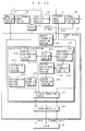
- FIG. 1 is a block diagram showing a structure of a memory control unit according to a first embodiment of the present invention.
- the memory control unit according to the first embodiment comprises a transfer-target unit 11, an address generator 12, a command generator 13, a data processor 14, and SDRAM 15.
- the memory control unit according to the first embodiment of the present invention is effective in the case where data transfer is continuously performed across a bank boundary from an address in one bank (hereinafter, represented by a bank 0) to an address in the other bank (hereinafter, represented by a bank 1) in SDRAM 15 (refer to FIG. 27 ), especially in the case where the number of bytes of the first data transfer with respect to the bank 0 is not more than the burst length.
- the transfer-target unit 11 outputs commands such as a start address (a virtual address), a transfer size, and read (or write) for data to be read (or written), to the address generator 12.
- the address generator 12 receives the commands from the transfer-target unit 11, then generates control signals for a start address (a physical address), a burst length, and read (or write) which are obtained by dividing the commands into a plurality of instructions for data transfer, and outputs the signals to the command generator 13.
- the address generator 12 also generates transferred-byte-number information representing the number of bytes of the data first transferred by read access up to a boundary in the burst length, and outputs the information to the command generator 13.
- the command generator 13 generates a clock and control commands designating page (row) / column addresses in accordance with the control signals received from the address generator 12, and outputs them to SDRAM 15.
- the command generator 13 evaluates the number of bytes in the transferred-byte-number information, and thereby controls SDRAM 15 so that it executes instructions in order from an instruction capable of increasing its data transfer rates. That is to say, when data is read across the bank boundary in SDRAM 15 as in the above description, the command generator 13 judges which is to be first executed between read processing to the bank 0 and activation processing to the bank 1, thereby controlling SDRAM 15.
- a read command is executed so as to start reading of data in the bank 0 first, and when the number is smaller than the number of cycles of the CAS latency, an active command is executed so as to complete entire data reading in the minimum number of clocks.
- the command generator 13 outputs control commands instructing read (or write) to the data processor 14.
- the data processor 14 receives the control commands for data read from the command generator 13, then reads data from SDRAM 15 in synchronization with the clock described above, and transfers the data to the transfer-target unit 11 (or receives the control commands for data write, then reads data from the transfer-target unit 11, and transfers the data to SDRAM 15 in synchronization with the clock described above).
- SDRAM 15 is synchronous dynamic random access memory operating in response to the control commands outputted from the command generator 13.
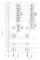
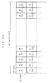
- FIGS. 2 to 4 show examples of data read timing in the case where data is continuously read across the bank boundary.
- FIG. 2 shows two types of data read timing in the case where a total of ten pieces of data, i.e., data a1 and a2 in the bank 0 and data b1 to b8 in the bank 1 are continuously read across the bank boundary.
- FIG. 3 shows two types of data read timing in the case where a total of eleven pieces of data, i.e., data a1 to a3 in the bank 0 and data b1 to b8 in the bank 1 are continuously read across the bank boundary.
- FIG. 4 shows two types of data read timing in the case where a total of twelve pieces of data, i.e., data a1 to a4 in the bank 0 and data b1 to b8 in the bank 1 are continuously read across the bank boundary.
- FIGS. 2 to 4 The contents shown by FIGS. 2 to 4 are each described first. Processing shown in (a) of FIG. 2 is the same as that in FIG. 32 described above.
- the "Ra” command is first issued and then the “Ab” command is issued next, thereby taking twenty-one cycles to terminate entire data reading.
- the "Ab” command is first issued and then "Ra” command is issued. Resultantly, a cycle in which first data is read is delayed, however, it takes only twenty cycles to terminate the entire data reading.
- the number of cycles required to terminate the entire data reading changes depending on which is first issued between the Ra command and the Ab command, that is determined based on the number of bytes of data to be first transferred in the bank 0. From the specific examples in FIGS. 2 to 4 , it is clear that the number of cycles changes depending on whether the data length of transferred data is larger or smaller than the CAS latency "3".
- the conventional memory control unit can perform only the procedure of issuing the "Ra” command first and then the "Ab” command next (the processing shown in (a) of FIGS. 2 to 4 ) because of the fixed rule and constraint, resulting in degradation in data transfer efficiency in some cases.
- the address generator 12 calculates the number of bytes to be first transferred in the bank 0, and sends it as the transferred-byte-number information to the command generator 13.
- the command generator 13 evaluates the number of transferred bytes obtained as the transferred-byte-number information for the data to be first transferred in the bank 0, and compares the number with the predetermined CAS latency, thereby controlling SDRAM 15.
- the command generator 13 for example, is previously provided with a threshold value "3". Then, the command generator 13 controls SDRAM 15 so that SDRAM 15 issues the Ab command first (the processing shown in (b) of FIG. 2 ) in the case of the inputted number of transferred bytes X ⁇ 3, or issues the Ra command first (the processing (a) of FIGS. 3 and 4 ) in the case of X ⁇ 3. It is thus possible to increase the data transfer efficiency of SDRAM 15.
- the command generator 13 judges which is first issued between the Ra command and the Ab command, based on the transferred-byte-number information generated in the address generator 12, thereby controlling the processing of SDRAM 15. In this way, in the case where data reading is continuously performed in different banks, commands are issued such that data transfer can be always terminated in a minimum cycle. Thus, the number of cycles required for two continuous access (access to the banks 0 and 1) can be reduced, making it possible to increase actual transfer rates of SDRAM 15.
- the application of the present memory control unit is not limited to the above case and the data-transfer-cycle can be optimized in the other conditions by controlling commands according to the same ideas as in the above.
- FIG. 5 is a block diagram showing a structure of a memory control unit according to a second embodiment of the present invention.
- the memory control unit according to the second embodiment comprises a transfer-target unit 21, an address generator 22, a command generator 23, a data processor 24, SDRAM 25, and a counter 26.
- the memory control unit according to the second embodiment of the present invention is effective in the case where data transfer is continuously performed with respect to an address in a bank 0 in SDRAM 25, then an address in a bank 1 across a bank boundary, and next to another address in the bank 0.
- the transfer-target unit 21 outputs commands such as a start address (a virtual address), a transfer size, and read (or write) which relate to data to be read (or written), to the address generator 22.
- the address generator 22 receives the commands from the transfer-target unit 21, then generates control signals for a start address (a physical address), a burst length, and read (or write) which are obtained by dividing the commands into a plurality of instructions for data transfer, and outputs the signals to the command generator 23.
- the address generator 22 also outputs a transfer-data-size which represents a size of data to be first transferred from/into the bank 0, to the counter 26.
- the counter 26 counts the number of times of issuing read (or write) commands in the command generator 23, and with each count subtracts a size of transferred data, i.e. , the burst length which is a size of data capable of being transferred by one burst instruction to SDRAM 25 from the transfer size supplied from the address generator 22.
- the transfer size after the subtraction that is the remainder of data to be transferred
- the counter 26 then notifies the command generator 23 of the fact.
- the command generator 23 generates control commands designating page (row) /column addresses in accordance with a clock and the control signals received from the address generator 22, and outputs control commands to SDRAM 25.
- the command generator 23 when received the notification from the counter 26, converts a read (or write) command to the bank 0 to be issued to SDRAM 25 into a read (or write) command accompanied by the next precharge command to the bank 0, and sends it to SDRAM 25.
- the read (or write) command accompanied by the precharge command is, when the currently-performed transfer processing in the bank 0 is terminated, for performing the next precharge processing in the bank 0 without issuing a precharge command during performing transfer processing in the bank 1.
- the command generator 23 also outputs a control command instructing read (or write), to the data processor 24.
- the data processor 24 reads data from SDRAM 25 in synchronization with the clock in response to control commands for data read outputted from the command generator 23, and transfers the data to the transfer-target unit 21 (or reads data from the transfer-target unit 21 in response to control commands for data write and transfers the data to SDRAM 25 in synchronization with the clock).
- SDRAM 25 is synchronous dynamic random access memory which receives the control commands outputted from the command generator 23 to operate.
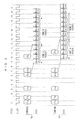
- FIG. 6 is two types of data read timing in the case where a total of twelve pieces of data a1 to a 8 in the bank 0 and data b1 to b4 in the bank 1 are continuously read across a bank boundary, and then data a9 to a12 in the bank 0 are read in succession.
- Processing in (a) of FIG. 6 shows the data read timing in the conventional memory control unit as shown in FIG. 29 .
- Processing in (b) of FIG. 6 shows data read timing in the memory control unit according to the second embodiment.
- precharge commands to the banks 0 and 1 are represented by “Pa” and “Pb”, respectively, active commands to the banks 0 and 1 are represented by “Aa” and “Ab” , respectively, a read command to the bank 1 is represented by “Rb”, and a read command with precharge to the bank 0 is represented by "RawP”.
- CAS latency is "2" clocks and a burst length is "4" data.
- the command generator 83 issues the Pa command first to read data in the bank 0 containing data a1 to a8 (in the zeroth cycle).
- the Pb command to the bank 1 is then issued utilizing the CAS latency interval (2 clocks) (in the first cycle).
- the Aa command is issued at the second clock from the issue of the Pa command (in the second cycle).
- the first Ra command is issued (in the fourth cycle), thereby transferring data a1 to a4 (because the burst length is "4").
- the Ab command is issued during the data transfer in the bank 0, so as to access the bank 1 any time (in the fifth cycle).
- the second Ra command is issued in the eighth cycle so as to start transferring data a5 to a8 immediately after the data a4 is transferred.
- the command generator 83 then issues the Rb command in the twelfth cycle so that the data b1 to b4 in the bank 1 can be transferred immediately after the data transfer in the bank 0 is terminated. From then on, in order to transfer the data a9 to a12 existing in the other addresses in the bank 0, the Pa, Aa and Ra commands are issued at intervals of two clocks in accordance with the CAS latency (in the thirteenth, fifteenth and seventeenth cycles).
- the memory control unit solves the above problem with the following method. It should be noted that, as described earlier, the address generator 22 outputs "8" which is the number of the data a1 to a8 to be first transferred in the bank 0, to the counter 26 as the transfer size in the above condition (refer to FIG. 5 ).
- the processing shown in (b) of FIG. 6 is the same as the above-described processing up to the fifth cycle in the drawing.
- the command generator 23 next issues the second Ra command in the eighth cycle so as to start transferring the data a5 to a8 immediately after the data a4 is transferred.
- the second Ra command issued at this time is the RawP command which is the read command with precharge, and outputted in response to the notification received from the counter 26.
- the RawP command allows SDRAM 25 to perform precharge processing at its own discretion without receiving the Pa command again from the command generator 23, in the thirteenth cycle in which the data a8 can be transferred without problems.
- the Aa command and the Ra command can be issued each one cycle earlier (in the fourteenth and sixteenth cycles).
- the counter 26 counts the number of times the read commands are issued by the command generator 23, thereby detecting the last data transfer in one bank to which processing is to be performed.
- the command generator 23 issues the read command with precharge, to control the processing in SDRAM 25.
- precharge processing for the other data is automatically executed. Accordingly, the precharge processing is started without delay even when the timing of issuing the precharge command matches the timing of issuing the other subsequent command, making it possible to increase the effective transfer rates of SDRAM 25.
- the application of the present memory control unit is not limited to the above case and the data-transfer-cycle can be optimized in the other conditions by controlling commands according to the same idea as in the above.
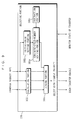
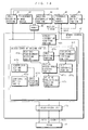
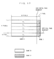
- FIG. 7 is a block diagram showing a structure of a memory system according to a third embodiment of the present invention.
- the memory system according to the third embodiment comprises transfer-target units 31 to 33, an arbiter 30, an SDRAM controller 34, and SDRAM 35.
- Each of the transfer-target units 31 to 33 outputs a transfer request signal to the arbiter 30 when requested to transfer data with SDRAM 35, and then outputs transfer information to the SDRAM controller 34 when receiving a transfer enabling signal returned from the arbiter 30.
- the arbiter 30 always monitors whether each transfer-target unit is transferring data with SDRAM 35 or not. When acquired transfer request information from any one of the transfer-target units, the arbiter 30 returns a transfer enabling signal to the transfer-target unit which outputs the transfer request information, at the time when data transfer to/from all transfer-target units is terminated. Moreover, when acquired transfer request information from a plurality of transfer-target units, the arbiter 30 selects one of them, then returns a transfer enabling signal to the transfer-target unit which outputs the selected transfer request information, and processes the other transfer request information which are not selected this time in the same way. The selection method here will be described later in detail.
- the SDRAM controller 34 generates control commands such as CLK, RAS, CAS, WE and an access address and the like based on the transfer information outputted from the transfer-target unit, and outputs the commands to SDRAM 35, thereby realizing data transfer between SDRAM 35 and the transfer-target unit which outputs the transfer information.
- Some SDRAM controllers 34 are constituted by the address generator 12, the command generator 13, and the data processor 14 as described in the first embodiment, and the other SDRAM controller 34 is constituted by the address generator 22, the command generator 23, the data processor 24, and the counter 26 as described in the second embodiment.
- SDRAM 35 has the same features as typical SDRAM described earlier, and is controlled by the control commands acquired from the SDRAM controller 34.
- FIG. 8 shows a detailed structure of the arbiter 30.
- the arbiter 30 comprises a transfer-request-information receiving portion 301, a transfer-request-information holding portion 302, a tail specifying portion 303, and a head specifying portion 304, and a selecting portion 305.
- the transfer-request-information receiving portion 301 accepts the transfer request information issued by the transfer-target units 31 to 33, respectively.
- the transfer request information includes memory area information indicating memory areas to be accessed, and limit information indicating time limits for transfer pending.
- the memory area information includes a physical address in SDRAM 35, a bank number in SDRAM 35, or a pair of a bank number and a page number in SDRAM 35, for example.
- the limit information includes a limit cycle number representing limits for the number of cycles permitted from the issue of the transfer request information to the completion of the corresponding transfer, for example.
- the transfer-request-information holding portion 302 holds each transfer request information accepted by the transfer-request-information receiving portion 301 until the corresponding transfer is allowed.
- the tail specifying portion 303 specifies a tail bank to be accessed at the last, or a pair of a tail bank and a tail page to be accessed at the last, in currently-accessed transfer request information or in preceding transfer request information to be accessed with higher priority.
- the head specifying portion 304 specifies for each transfer request information a head bank to be accessed first, or a pair of a head bank and a head page to be accessed first.
- the selecting portion 305 selects access to a memory area indicated by the transfer request information corresponding to the head bank representing a different bank from the tail bank, prior to access to a memory area indicated by transfer request information corresponding to the head bank representing the same bank as the tail bank.
- the selecting portion 305 selects access to a memory area indicated by the transfer request information corresponding to the head bank representing a different bank from the tail bank , and access to a memory area indicated by the transfer request information corresponding to the head bank representing the same bank as the tail bank and also corresponding to the head page representing the same page as the tail page, prior to access to a memory area indicated by the transfer request information corresponding to the head bank representing the same bank as the tail bank and also corresponding to the head page representing a different page from the tail page.
- the selecting portion 305 thus defines order of access immediately after the access to the memory area indicated by the preceding transfer request information. Besides, the selecting portion 305 judges whether each transfer request information is to exceed the limits indicated by the limit information or not, and thereby selects with the highest priority access to a memory area indicated by the transfer request information which is judged to most likely exceed the limits.
- FIG. 9 shows an example of a structure of the selecting portion 305 in FIG. 8 . It is possible that the selecting portion 305 has the structure including a remaining-cycle-number holding portion 305a, an initial-value setting portion 305b, a subtraction portion 305c, a calculation portion 305d, and a judging portion 305e as shown in FIG. 9 , for example.
- the remaining-cycle-number holding portion 305a holds for each transfer request information the remaining number of cycles representing limits for the number of cycles permitted from the present time until the transfer is completed.
- the initial-value setting portion 305b makes the remaining-cycle-number holding portion 305a hold the limit cycle number as an initial value of the remaining cycle number when the transfer request information is issued.
- the subtraction portion 305c subtracts one from the remaining cycle number held in the remaining-cycle-number holding portion 305a in each cycle.
- the judging portion 305e judges that the corresponding transfer request information is to exceed the limits in the case of "the prospective cycle number for completion > the remaining cycle number".
- FIG. 10 shows another example of the structure of the selecting portion 305 in FIG. 8 . It is also possible to include in the structure of the selecting portion 305 a counting portion 305f, a calculating portion 305g, and a judging portion 305h as shown in FIG. 10 , for example.
- the counting portion 305f counts the number of queued cycles for each transfer request information in cycles from when the transfer request information is issued.
- the judging portion 305h judges that in the case of "the prospective cycle number for completion > the limit cycle number", the corresponding transfer request information is to exceed the limits indicated by the limit information.
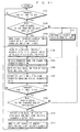
- FIG. 11 is a flow chart delineating a method of optimizing order of executing access in the memory system according to the third embodiment of the present invention.
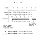
- FIG. 12 shows order of transfer in operation clocks in the case where the data transfer as shown in FIG. 33 is simultaneously requested from the transfer-target units in the memory system according to the third embodiment of the present invention. It is also assumed in FIG. 12 that CAS latency is 3 and a burst length is 8. Since the CAS latency is 3 as in the case with FIG.
- the transfer request information corresponding to each data transfer is always issued from each transfer-target unit, the transfer-request-information receiving portion 301 always accepts the issued transfer request information, and the transfer-request-information holding portion 302 holds the transfer request information until the corresponding transfer is permitted.
- the initial-value setting portion 305b makes the remaining-cycle-number holding portion 305a hold each limit cycle number as an initial value of the remaining cycle number, and then the subtraction portion 305c subtracts one from the remaining cycle number in each cycle. It is assumed here that the transfer-target units simultaneously issue transfer request information corresponding to the data transfer as shown in FIG. 33 .
- the transfer-target unit 31 issues transfer request information including pairs of a bank number and a page number which align in order that they are accessed, i.e., "the page 0 in the bank 0, the page 0 in the bank 1, the page 0 in the bank 0, and the page 0 in the bank 1", and the limit cycle number "100"
- the transfer-target unit 32 issues transfer request information including a pair of a bank number and a page number to be accessed, i.e., "the page 1 in the bank 1", and the limit cycle number "100”
- the transfer-target unit 33 issues transfer request information including a pair of a bank number and a page number to be accessed, i.e., "the page 1 in the bank 0", and the limit cycle number "100”.
- the arbiter 30 judges whether there is transfer request information held in the transfer request information holding portion 302 or not (step S101). The judgement in step S101 is repeated until the transfer request information is found. In this example, the three pieces of transfer request information are held in the transfer-request-information holding portion 302, and therefore it is judged as Yes. The arbiter 30 then judges whether there are more than or equal to two pieces of transfer request information held in the transfer-request-information holding portion 302 or not (step S102). In this example, the three pieces of transfer request information are held in the transfer-request-information holding portion 302, and therefore it is judged as Yes.
- step S102 When the arbiter 30 judges that there are more than or equal to two pieces of transfer request information (as Yes) in step S102, the selecting portion 305 once selects transfer request information issued by the highest-priority transfer-target unit first (step S103). On the other hand, when the arbiter 30 judges in step S102 that the transfer request information is less than two (as No), the selecting portion 305 arbitrarily selects one piece of transfer-request-information held in the transfer-request-information holding portion 302 (step S112), and then the procedure advances to step S105. In this example, the transfer request information issued by the transfer-target unit 31 is once selected.
- the judging portion 305e judges that the corresponding transfer request information is to exceed the limits, and selects the same prior to the transfer request information once selected in step S102 (step S104).
- the judging portion 305e selects access to memory areas indicated by the transfer request information with the highest priority.
- the arbiter 30 next returns a transfer enabling signal to the transfer-target unit corresponding to the transfer request information finally selected by the judging portion 305e, and deletes the corresponding transfer request information from the transfer-request-information holding portion 302 (step S105).
- the transfer enabling signal is returned to the transfer-target unit 31.
- the tail specifying portion 303 specifies a tail bank to be accessed at the last, or a pair of a tail bank and a tail page to be accessed at the last in the currently-accessed transfer request information or the transfer request information to be accessed with higher priority (step S106).
- "a tail bank 1 and a tail page 0" to be accessed last is assumed to be specified.
- the transfer-target unit after receiving the transfer enabling signal, transfers data with SDRAM 35 through the SDRAM controller 34 (step S107).
- the transfer-target unit 31 transfers data with SDRAM 35.
- the arbiter 30 judges again whether there is transfer request information held in the transfer-request-information holding portion 302 or not, just before the currently-performed data transfer is completed (step S108). When it is judged in step S108 that there is no transfer request information (as No), the procedure returns to step S101. In this example, the two pieces of transfer request information are held in the transfer-request-information holding portion 302, and therefore it is judged as Yes. To the contrary, when judging in step S108 that there is transfer request information, the arbiter 30 judges whether more than or equal to two pieces of transfer request information are held in the transfer-request-information holding portion 302, just before the currently-performed data transfer is completed (step S109). In this example, the two pieces of transfer request information are held in the transfer-request-information holding portion 302, therefore it is judged as Yes.
- the head specifying portion 304 specifies for each transfer request information, a head bank to be first accessed, or a pair of a head bank and a head page to be first accessed (step S110).
- the arbiter 30 arbitrarily selects one piece of transfer request information held in the transfer-request-information holding portion 302 (step S112), and then the procedure moves to step S105.
- the selecting portion 305 once selects access to the memory area indicated by the transfer request information based on the above-described contents (step S111).
- the selecting portion 305 once selects transfer request information issued by the highest-priority transfer-target unit first. Since "the tail bank 1" and "the tail page 0" are assumed in this example, the transfer request information issued by the transfer-target unit 32 corresponds to the head bank 1 representing the same bank as the tail bank 1, and to the head page 1 representing a different page from the tail page 0, and the transfer request information issued by the transfer-target unit 33 corresponds to the head bank 0 representing a different bank from the tail bank 1. Accordingly, the transfer request information issued by the transfer-target unit 33 is once selected prior to the transfer request information issued by the transfer-target unit 32.
- step S111 After the selection in step S111 is completed, the procedure returns to step S104, and the processing thereafter is continuously performed in accordance with the above-described procedure.
- the memory system optimizes the order of access to the memory areas indicated by all transfer request information held in the transfer-request-information holding portion 302 which should be accessed a plurality of times so as to decrease the frequency of continuous access to memory areas in the same bank, or so as to decrease the frequency of continuous access to memory areas in different pages in the same bank.
- the memory system thus controls processing for memory so that the memory areas in memory are accessed in accordance with the optimized access order.
- the numbers of cycles required until the end of the transfer in the conventional art and the present invention are compared below.
- the 69 cycles are required in the conventional art as shown in FIG. 34
- only 62 cycles are required in the present invention as shown in FIG. 12 . That is, the required number of cycles in the present invention is fewer by the cycles of the overhead produced by the precharge command (seven cycles), which becomes unnecessary here.
- Data transfer is selected just before the previous data transfer is completed in the above description, however, data transfer may be selected with any timing before the previous data transfer is completed. Data transfer may be selected before the previous data transfer is started, of course, and therefore it is also possible to decide order of entire data transfer before the start of entire data transfer. Moreover, it is assumed here that the pairs of the bank number and the page number aligned in the order of access are included in the transfer request information, however, any information may be available if it can specify the head and tail. Besides, if at least information capable of specifying the head and tail banks is included in the transfer request information, the same effect can be obtained by selecting the next data transfer such that the same bank number is not continuous.
- the transfer request information even if information capable of specifying the tail bank is not be included in the transfer request information, it may be acquired from the SDRAM controller 34. Furthermore, there is another variation that an address in memory to be accessed is included in the transfer request information and the arbiter 30 or the SDRAM controller 34 specifies a bank number and a page number based on the address.
- FIG. 13 is a block diagram showing a structure of an image decoding system (a video decoder) using a memory control unit according to a fourth embodiment of the present invention.
- the image decoding system of the fourth embodiment comprises an image decoding portion 41, a difference-image buffer 42, a reference-image buffer 43, a half-pel interpolator 44, an adder 45, an image outputting portion 46, a memory controller 47, and SDRAM 48.
- the image decoding portion 41 decodes a coded reference image which is transmitted, and transfers the decoded reference image through the memory controller 47 to SDRAM 48.
- the image decoding portion 41 also decodes a coded difference image, and outputs the decoded difference image to the difference-image buffer 42, an address of the reference image to the reference-image buffer 43, and an interpolating method to the half-pel interpolator 44.
- the difference-image buffer 42 temporarily stores the decoded difference image, and adjusts operation timing of the adder 45.
- the reference-image buffer 43 reads the reference image specified by the image decoding portion 41 from the memory controller 47, and temporarily stores the image to output to the half-pel interpolator 44 as required.
- the half-pel interpolator 44 interpolates the reference images stored in the reference-image buffer 43 according to the interpolating method specified by the image decoding portion 41, and outputs the images to the adder 45.
- the interpolating method performed here does not directly relate to the subjects of the present invention, and therefore its description is omitted here.
- the adder 45 adds the difference image held by the difference-image buffer 42 and the reference image held by the reference-image buffer 43 to obtain an output image, and transfers the image through the memory controller 47 to SDRAM 48.
- the image outputting portion 46 reads the decoded image data through the memory controller 47 from SDRAM 48 in step with the timing of outputting the image, and outputs the data.
- the memory controller 47 controls the transfer of the decoded image data from the image decoding portion 41 to SDRAM 48, the transfer of the reference image from SDRAM 48 to the reference-image buffer 43, the transfer of the output image from the adder 45 to SDRAM 48, and the transfer of the output image from SDRAM 48 to the image outputting portion 46.
- SDRAM 48 has the same structure and features as SDRAM 35 in the third embodiment.
- the image data of respective output images obtained in the adder 45 are stored in respective unit areas in SDRAM 48 each of which is composed of only a memory area of a single page in a single bank in predetermined order that the data is continuous in the display state.
- the unit areas contiguous to each other in storage order are composed of different banks.
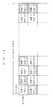
- FIG. 14 shows bank numbers and page numbers of memory areas in which image data is stored, in the case where the image data, whose amount per one pixel (the amount represents "brightness", for example) is 8 bits, of "16 ⁇ (2n + 1)" pixels wide which is composed of rectangle unit areas each of 16 pixels wide by 32 pixels high is stored in SDRAM 48 comprising two banks (banks 0 and 1) in which a bit width of a data bus is 8 bits, one column is 8 bits and one page includes 512 columns.
- "n" is an integer of not less than 1.
- FIG. 15 is the same as FIG. 14 except that the number of pixels in the horizontal direction of the image data to be stored in FIG. 15 is "16 ⁇ 2n".
- each of the rectangle areas divided by solid lines is a memory area composed of a single page, and rectangle areas without shading represent the bank 0 and shaded rectangle areas represent the bank 1.
- data in single-page rectangle areas which are contiguous to each other in the vertical and horizontal directions are stored in the different banks.
- data in single-page rectangle areas which are contiguous to each other in the horizontal direction are stored in the different banks, however, data in single-page rectangle areas which are contiguous to each other in the vertical direction are stored in the same bank.
- FIG. 16 shows an example of a reference image read from the image data stored in SDRAM 48 as shown in FIG. 14 .
- FIG. 17 shows an example of a reference image read from the image data stored in SDRAM 48 as shown in FIG. 15 .
- the reference images shown in FIGS. 16 and 17 are each represented by a rectangle area of 9 pixels wide by 5 pixels high, and are generally read in display order, that is, the order of read becomes as "a1 ⁇ a2 ⁇ b1 ⁇ b2 ⁇ c1 ⁇ c2 ⁇ d1 ⁇ d2 ⁇ e1 ⁇ e2".
- the memory control unit 47 is constituted by an access-information accepting portion 471, an access-order optimizing portion 472, and an SDRAM controller 473.
- the access-information accepting portion 471 accepts an address of a reference image to be read as access information from the reference-image buffer 43.
- the access-order optimizing portion 472 optimizes order of access to reference images to be read so as to decrease the frequency of continuous access to memory areas in the same bank.
- the SDRAM controller 473 generates control commands based on respective transfer requests from the image decoding portion 41, the reference-image buffer 43, the adder 45, and the image outputting portion 46, and outputs the commands to SDRAM 48, thereby realizing data transfer. Especially when the reference image is read, the SDRAM controller 473 controls SDRAM 48 so that the memory areas in SDRAM 48 are accessed according to the access order optimized by the access-order optimizing portion 472.
- the access-order optimizing portion 472 includes an area dividing portion 472a, a vertical-page-boundary detecting portion 472b, a relative-access-order deciding portion 472c, a screen-size setting portion 472d, a configuration setting portion 472e, a bank judging portion 472f, a horizontal-page-boundary detecting portion 472g, a size comparing portion 472h, and an initial-access-order deciding portion 472i.
- the area dividing portion 472a divides a memory area in SDRAM 48 indicated by an address of a reference image to be read into continuous single-page areas each of which is a memory area composed of a single page.
- the memory area is divided into single-page areas of "a1, a2, b1, b2, c1, c2, d1, d2, e1 and e2".
- the vertical-page-boundary detecting portion 472b detects a boundary between unit areas which are contiguous to each other in the display state but not in the storage order.
- the vertical-page-boundary detecting portion 472b always monitors whether a head address of a horizontal line requested for transfer is in the different unit area from a head address of a horizontal line to be requested for the next transfer or not. When detecting that they are in the different unit areas, the vertical-page-boundary detecting portion 472b judges to detect a vertical page boundary, and outputs a vertical-page-cross signal to the SDRAM controller 473. It should be noted that the vertical page boundary is detected here since the storage order of the unit areas is continuous in the horizontal direction, however, a horizontal page boundary is detected when the storage order is continuous in the vertical direction. In FIGS. 16 and 17 , the vertical page boundaries as shown in the drawings are detected.
- the relative-access-order deciding portion 472c decides order of access to the single-page areas depending on whether unit areas vertically contiguous to each other across the vertical page boundary are composed of the same bank or the different banks. More specifically, when the unit areas contiguous to each other across the vertical page boundary are composed of the same bank, the order of access to the single-page areas below the vertical page boundary is defined as the same as the order of access to the single-page areas above the vertical page boundary, to the contrary, when the contiguous unit areas are composed of the different banks, the access order of the single-page areas below the vertical page boundary is defines as the reverse to the access order of the single-page areas above the vertical page boundary.
- the screen-size setting portion 472d sets the number of pixels which are continuous in the storage order and in the display state as a screen size in the image data stored in SDRAM 48 in response to an instruction from the external.
- the screen size here is the number of horizontal pixels of the image data to be decoded, that is, "16 ⁇ (2n + 1)" in the example of FIG. 14 and " 16 ⁇ 2n” in the example of FIG. 15 .
- the configuration setting portion 472e sets a shape of the unit area in response to an instruction from the external. In the examples shown in FIGS. 14 and 15 , the unit area is a rectangle-shaped area of 16 pixels wide by 32 pixels high.
- the bank judging portion 472f judges whether the unit areas contiguous to each other across the vertical page boundary are composed of the same bank or the different banks based on the screen size and the shape of the unit area in the case where the generated image data is stored in the above-described order that the data is continuous in the display state.
- the data in the single-page rectangle areas vertically contiguous to each other is stored in the different banks, and therefore it is judged that the data is composed of the different banks.
- the data in the single-page rectangle areas vertically contiguous to each other is stored in the same bank, and therefore it is judged that the data is composed of the same bank.
- the horizontal-page-boundary detecting portion 472g detects a boundary between unit areas contiguous to each other in the display state and storage order. More specifically, a boundary between unit areas in a horizontal line is detected as a horizontal page boundary. It should be noted that the horizontal page boundary is detected since the storage order of the unit areas here is continuous in the horizontal direction, however, a vertical page boundary is detected when the order is continuous in the vertical direction. In FIGS. 16 and 17 , the horizontal page boundaries as shown in the drawings are detected.
- the size comparing portion 472h compares size of respective memory areas obtained by dividing the reference image by the horizontal page boundary. In FIGS. 16 and 17 , it is judged that the memory area on the right side is smaller than that on the left side.
- the initial-access-order deciding portion 472i decides that the single-page areas above the vertical page boundary are read in order that the single-page areas belonging to the memory area judged to be smaller by the size comparing portion 472h are read first.
- the order of access to the lines above the vertical page boundary is from right to left, and the order of access to the lines below the vertical page boundary is from left to right. Therefore, the read order in this case becomes as "a2 ⁇ a1 ⁇ b2 ⁇ b1 ⁇ c2 ⁇ c1 ⁇ d2 ⁇ d1 ⁇ e1 ⁇ e2".
- the order of access to the lines above the vertical page boundary is from right to left, and the order of access to the lines below the vertical page boundary is also from right to left. Therefore, the read access in this case becomes as "a2 ⁇ as b2 ⁇ be c2 ⁇ c1 ⁇ d2 ⁇ d1 ⁇ e2 ⁇ e1".
- FIG. 18 is a flow chart delineating a method of optimizing the order of executing access in the memory control unit according to the fourth embodiment of the present invention.
- the access-information accepting portion 471 accepts access information (step S201). It is assumed in this example that access information about read of the reference image shown in FIG. 16 is accepted.
- the area dividing portion 472a divides a memory area in SDRAM 48 indicated by an address of the reference image to be read into single-page areas (step S202). In this example, the memory area is divided into single-page areas of "a1, a2, b1, b2, c1, c2, d1, d2, e1 and e2" shown in FIG. 16 .
- the horizontal-page-boundary detecting portion 472g detects a horizontal page boundary (step S203). In this example, the horizontal page boundary as shown in FIG. 16 is detected.
- the size comparing portion 472h compares size of the memory areas into which the reference image is divided by the horizontal page boundary(step S204). In this example, the memory area on the right side are judged to be smaller than that on the left side.
- the relative-access-order deciding portion 472c decides that the lines above the vertical page boundary are accessed and read in ascending order of size of the memory areas (step S205).
- the memory area on the right side is smaller, and therefore is decided to be read first.
- the read order becomes as "a2 ⁇ a1 ⁇ b2 ⁇ b1 ⁇ c2 ⁇ c1 ⁇ d2 ⁇ d1".
- the SDRAM controller 473 controls SDRAM 48 so that the lines above the vertical page boundary are accessed in the order decided by the relative-access-order deciding portion 472c (step S206).
- the SDRAM controller 473 controls SDRAM 48 so that the memory area on the right side is read first.
- the vertical-page-boundary detecting portion 472b detects a vertical page boundary (step S207), and when detecting the boundary, outputs a vertical-page-cross signal to the SDRAM controller 473 (step S208).
- the vertical page boundary as shown in FIG. 16 is detected.
- the bank judging portion 472f judges whether the unit areas contiguous to each other across the vertical page boundary are composed of the same bank or the different banks, based on the screen size set by the screen-size setting portion 472d and the shape set by the configuration setting portion 472e (step S209).
- the unit areas are judged to be composed of the different banks as shown in FIG. 14 , based on the screen size of "16 ⁇ (2n + 1)" and the shape of "a rectangle area of 16 pixels wide by 32 pixels high”.
- the relative-access-order deciding portion 472c defines the order of access to the single-page areas below the vertical page boundary as the same as the order of access to the single-page areas above the vertical page boundary (step S210).
- the relative-access-order deciding portion 472c defines the order of access to the single-page areas below the vertical page boundary as the reverse to the order of access to the single-page areas above the vertical page boundary (step S211).
- the access order of the single-page areas below the vertical page boundary is decided as order that the memory area on the left side is first read, that is, the read order becomes as "e1 ⁇ e2".
- the SDRAM controller 473 controls SDRAM 48 so that the lines below the vertical page boundary are accessed in the order decided by the relative-access-order deciding portion 472c (step S212).
- the SDRAM controller 473 controls SDRAM 48 so that the memory area on the left side is first read. Accordingly, the read order of all single-page areas becomes as "a2 ⁇ a1 ⁇ b2 ⁇ b1 ⁇ c2 ⁇ c1 ⁇ d2 ⁇ d1 ⁇ e1 ⁇ e2".
- step S201 access information about read of the reference image shown in FIG. 17 is accepted in step S201.
- step S202 the memory area is divided into single-page areas of "a1, a2, b1, b2, c1, c2, d1, d2, e1 and e2" shown in FIG. 17 .
- step S203 the horizontal page boundary as shown in FIG. 11 is detected.
- step S204 the memory area on the right side is smaller than that on the left side.
- step S205 it is decided that the memory area on the right side is to be first read since it is smaller, and specifically, read order is decided as "a2 ⁇ a1 ⁇ b2 ⁇ b1 ⁇ c2 ⁇ c1 ⁇ d2 ⁇ d1".
- step S206 SDRAM 48 is controlled so that the memory area on the right side is first read. After the read order is decided as "a2 ⁇ a1 ⁇ b2 ⁇ b1 ⁇ c2 ⁇ c1 ⁇ , d2 ⁇ d1", the vertical page boundary as shown in FIG. 17 is detected in step S208.
- step S209 it is judged that the unit areas are composed of the same bank as shown in FIG. 15 , based on the screen size of "16 ⁇ 2n" and the shape of "a rectangle area of 16 pixels wide by 32 pixels high".
- steps S210 and S211 the unit areas are composed of the same bank as shown in FIG.
- the access order is decided as the order that the memory area on the right side is first read, that is "e2 ⁇ e1".
- step S212 SDRAM 48 is controlled so that the memory area on the right side is first read. Therefore, the read order of all single-page areas becomes as "a2 ⁇ a1 ⁇ b2 ⁇ b1 ⁇ c2 ⁇ c1 ⁇ d2 ⁇ d1 ⁇ e2 ⁇ e1".
- Processing in (a) of FIG. 19 shows read timing in operation clocks in the case where the reference image shown in FIG. 16 is read from the image data stored as in FIG. 14 in the image decoding system according to the fourth embodiment.
- Processing in (b) of FIG. 19 shows read timing in operation clocks in the case where the reference image shown in FIG. 16 is read from the image data stored as in FIG. 14 in order of address in a conventional image decoding system.
- FIG. 20 shows read timing in operation clocks in the case where the reference image shown in FIG. 17 is read from the image data stored as in FIG. 15 in the image decoding system according to the fourth embodiment.
- CAS latency and a burst length are assumed to be 3 and 8, respectively, in the processing in (a) and (b) of FIG. 19 and FIG. 20 .
- read data until one clock after a precharge command is inputted is effective, and an interval between a precharge command and an active command and an interval between an active command and a read command to the same bank must be both more than or equal to 3 clocks. It is also assumed that an interval between active commands to the different banks must be 3 clocks.
- processing shown in (a) of FIG. 19 , processing (b) of FIG. 19 , and processing in FIG. 20 require 53, 58, 59 cycles, respectively, to read entire reference images.
- FIG. 21 shows bank numbers and page numbers of memory areas in which image data is stored, in the case where the image data, whose amount per one pixel (the amount represents "brightness", for example) is 8 bits, of "16 ⁇ (4n)" pixels wide which is composed of rectangle unit areas each of 32 pixels wide by 32 pixels high is stored in SDRAM 48 comprising two banks (banks 0 and 1) in which a bit width of a data bus is 8 bits, one column is 8 bits and one page includes 1028 columns. Note that "n” is an integer of not less than 1. In FIG. 21 , as in the case with FIG.
- FIG. 22 is the same as FIG. 21 except that the number of horizontal pixels of image data to be stored is "16 ⁇ (4n + 1)". Access order in this case, therefore, is defined as an order from right to left, independently of the presence of the vertical-page-cross signal.
- FIG. 23 is the same as FIG. 21 except that the number of horizontal pixels of image data to be stored is "16 ⁇ (4n + 2)".
- the data in single-page rectangle areas vertically and horizontally contiguous to each other are stored in the different banks. Access order in this case, therefore, is defined as the same as that in the case in FIG. 15 .
- FIG. 24 is the same as FIG. 21 except that the number of horizontal pixels of image data to be stored is "16 ⁇ (4n + 3)". Access order in this case is defined as an order from left to right, independently of the presence of the vertical-page-cross signal.
- the memory control unit optimizes the order of access to the reference image so that the frequency of continuous access to the memory areas in the same bank is decreased, or the frequency of continuous access to the memory areas in different pages in the same bank, and controls processing for memory so that the memory areas in memory are accessed according to the optimized access order.
- FIG. 25 is a block diagram showing a structure of an image decoding system (a video decoder) using a memory control unit according to a fifth embodiment of the present invention.
- the image decoding system comprises the image decoding portion 41, the difference-image buffer 42, the reference-image buffer 43, the half-pel interpolating portion 44, the adder 45, the image outputting portion 46, a memory controller 57, and SDRAM 48.
- the image decoding system according to the fifth embodiment has a structure in which the memory controller 47 in the image decoding system according to the fourth embodiment is replaced by the memory controller 57. Therefore, the other structure of the image decoding system according to the fifth embodiment is the same as that of the image decoding system according to the fourth embodiment, and the same reference numerals are assigned thereto and its explanation is omitted here.
- the memory controller 57 is constituted by the access-information accepting portion 471, an access-order optimizing portion 572, and the SDRAM controller 473.
- the access-order optimizing portion 572 includes the area dividing portion 472a, the vertical-page-boundary detecting portion 472b, the screen-size setting portion 472d, the configuration setting portion 472e, the bank judging portion 472f, the horizontal-page-boundary detecting portion 472g, the size comparing portion 472h, the initial-access-order deciding portion 472i, an address converting portion 572j, and an order reversing portion 572k.
- the access-order optimizing portion 572 has a structure in which the relative-access-order deciding portion 472c is deleted from the access-order optimizing portion 472 in the fourth embodiment and the address converting portion 572j and the order reversing portion 572k are added thereto. Therefore, the other structure of the access-order optimizing portion 572 in the fifth embodiment is the same as that of the access-order optimizing portion 472 in the fourth embodiment, and the same reference numerals are assigned thereto and its explanation is omitted here.
- the address converting portion 572j in the case where generated image data is stored in predetermined order that memory areas are continuous in the display state as in the fourth embodiment and when the bank judging portion 472f judges that the unit areas contiguous to each other across the vertical page boundary are composed of the same bank, converts between a logical address in the image data and a physical address in SDRAM 48 so that the unit areas are composed of different banks.
- the address converting portion 572j performs no processing.
- the address converting portion 572j since the data in single-page rectangle areas vertically contiguous to each other are judged to be stored in the same bank, the address converting portion 572j converts between the logical address in the image data and the physical address in SDRAM 48.
- the memory area in the bank 0 and the memory area in the bank 1 which are horizontally contiguous to each other are interchanged (for example, in even-numbered columns) every other rows consisting of memory areas.
- the order reversing portion 572k defines order of access to the single-page areas below the vertical page boundary as the reverse to order of access to the single-page areas above the vertical page boundary.
- FIG. 26 shows bank numbers and page numbers of memory areas in which image data is stored, in the case where the image data, whose amount per one pixel (the amount represents "brightness", for example) is 8 bits, of "16 ⁇ 2n" pixels wide which is composed of rectangle unit areas each of 16 pixels wide by 32 pixels high is stored in SDRAM 48 comprising two banks (banks 0 and 1) in which a bit width of a data bus is 8 bits, one column is 8 bits and one page includes 512 columns while the address converting portion 572j converts an address in the image data.
- “n” is an integer of not less than 1.
- the address converting portion 572j performs address conversion according to vertical positions of pixel as follows. Note that "m" is an integer of not less than one.
- the horizontal pixel number of the image data is "16 ⁇ (2n + 1)"
- the data in single-page rectangle areas which are contiguous to each other vertically and horizontally in the display state of the image data is stored in the different banks in SDRAM 48 even when no processing is performed, and therefore the address converting portion 572j performs no address conversion.
- the memory control unit converts between the logical address in the image data and the physical address in SDRAM 48 so that data in single-page rectangle areas vertically contiguous to each other is not stored in the same bank, then optimizes the order of access to the reference image so as to decrease the frequency of continuous access to memory areas in the same bank, or the frequency of continuous access to memory areas in different pages in the same bank, and thereby controls processing for memory so that the memory areas in memory are accessed according to the optimized access order.
- an image decoding system Although the examples of an image decoding system are described in the fourth and fifth embodiments, the present invention can be applied to an image encoding system (a video encoder).
Landscapes
- Engineering & Computer Science (AREA)
- Theoretical Computer Science (AREA)
- Physics & Mathematics (AREA)
- General Engineering & Computer Science (AREA)
- General Physics & Mathematics (AREA)
- Dram (AREA)
- Information Transfer Systems (AREA)
- Information Retrieval, Db Structures And Fs Structures Therefor (AREA)
- Compression Or Coding Systems Of Tv Signals (AREA)
Applications Claiming Priority (3)
| Application Number | Priority Date | Filing Date | Title |
|---|---|---|---|
| JP02365198A JP3922487B2 (ja) | 1998-02-04 | 1998-02-04 | メモリ制御装置および方法 |
| JP34452298A JP4234829B2 (ja) | 1998-12-03 | 1998-12-03 | メモリ制御装置 |
| EP99101569A EP0935199B1 (fr) | 1998-02-04 | 1999-02-02 | Unité et méthode de commande de mémoire et support comportant un programme de réalisation |
Related Parent Applications (1)
| Application Number | Title | Priority Date | Filing Date |
|---|---|---|---|
| EP99101569.4 Division | 1999-02-02 |
Publications (2)
| Publication Number | Publication Date |
|---|---|
| EP2357564A2 true EP2357564A2 (fr) | 2011-08-17 |
| EP2357564A3 EP2357564A3 (fr) | 2011-11-23 |
Family
ID=26361051
Family Applications (2)
| Application Number | Title | Priority Date | Filing Date |
|---|---|---|---|
| EP99101569A Expired - Lifetime EP0935199B1 (fr) | 1998-02-04 | 1999-02-02 | Unité et méthode de commande de mémoire et support comportant un programme de réalisation |
| EP11156809A Withdrawn EP2357564A3 (fr) | 1998-02-04 | 1999-02-02 | Unité et méthode de commande de mémoire et support comportant un programme de réalisation |
Family Applications Before (1)
| Application Number | Title | Priority Date | Filing Date |
|---|---|---|---|
| EP99101569A Expired - Lifetime EP0935199B1 (fr) | 1998-02-04 | 1999-02-02 | Unité et méthode de commande de mémoire et support comportant un programme de réalisation |
Country Status (4)
| Country | Link |
|---|---|
| US (1) | US6340973B1 (fr) |
| EP (2) | EP0935199B1 (fr) |
| CN (1) | CN1262929C (fr) |
| DE (1) | DE69943402D1 (fr) |
Cited By (1)
| Publication number | Priority date | Publication date | Assignee | Title |
|---|---|---|---|---|
| KR20200011136A (ko) * | 2018-07-24 | 2020-02-03 | 삼성전자주식회사 | 불휘발성 메모리 장치, 불휘발성 메모리 장치의 동작 방법 및 불휘발성 메모리 장치를 제어하는 메모리 컨트롤러의 동작 방법 |
Families Citing this family (23)
| Publication number | Priority date | Publication date | Assignee | Title |
|---|---|---|---|---|
| JP2000148997A (ja) * | 1998-11-13 | 2000-05-30 | Minolta Co Ltd | 画像処理装置 |
| JP2001356961A (ja) * | 2000-06-13 | 2001-12-26 | Nec Corp | 調停装置 |
| US7168093B2 (en) * | 2001-01-25 | 2007-01-23 | Solutionary, Inc. | Method and apparatus for verifying the integrity and security of computer networks and implementation of counter measures |
| JP2004520658A (ja) * | 2001-05-22 | 2004-07-08 | コーニンクレッカ フィリップス エレクトロニクス エヌ ヴィ | メモリへのアクセス速度を向上させる方法とシステム |
| JP3868250B2 (ja) * | 2001-10-09 | 2007-01-17 | 松下電器産業株式会社 | データ転送装置、データ転送システム、およびデータ転送方法 |
| JP3778055B2 (ja) * | 2001-11-02 | 2006-05-24 | ソニー株式会社 | 記録再生装置及び記録再生方法 |
| JP2003308246A (ja) * | 2002-04-17 | 2003-10-31 | Fujitsu Ltd | メモリコントローラのクロック制御装置及び方法 |
| CN100580640C (zh) * | 2003-01-27 | 2010-01-13 | 松下电器产业株式会社 | 存储器控制装置 |
| JP2005332370A (ja) * | 2004-04-19 | 2005-12-02 | Toshiba Corp | 制御装置 |
| JP4748641B2 (ja) * | 2004-12-06 | 2011-08-17 | ルネサスエレクトロニクス株式会社 | 情報処理システム |
| US7275143B1 (en) * | 2004-12-13 | 2007-09-25 | Nvidia Corporation | System, apparatus and method for avoiding page conflicts by characterizing addresses in parallel with translations of memory addresses |
| EP2003564A4 (fr) * | 2006-03-31 | 2009-11-25 | Panasonic Corp | Controleur de sortie de commande |
| CN101082852B (zh) * | 2006-05-29 | 2012-07-18 | 联阳半导体股份有限公司 | 用于存储器的控制装置及控制方法 |
| JP2008073895A (ja) * | 2006-09-19 | 2008-04-03 | Ricoh Co Ltd | 画像形成装置、画像形成方法、画像形成プログラム、及び、情報記録媒体 |
| DE102007005866B4 (de) * | 2007-02-06 | 2021-11-04 | Intel Deutschland Gmbh | Anordnung, Verfahren und Computerprogramm-Produkt zum Anzeigen einer Folge von digitalen Bildern |
| JPWO2009013879A1 (ja) * | 2007-07-20 | 2010-09-30 | パナソニック株式会社 | メモリーコントローラ、及びこれを用いた不揮発性記憶装置 |
| CN101539981B (zh) * | 2009-05-06 | 2011-07-20 | 成都市华为赛门铁克科技有限公司 | 一种数据安全控制方法、系统及传感器节点 |
| CN101692346B (zh) * | 2009-06-19 | 2013-06-26 | 无锡中星微电子有限公司 | 一种存储器数据采样装置及一种采样控制器 |
| US8392689B1 (en) * | 2010-05-24 | 2013-03-05 | Western Digital Technologies, Inc. | Address optimized buffer transfer requests |
| CN102402410A (zh) * | 2010-09-09 | 2012-04-04 | 奇景光电股份有限公司 | 显示装置及控制方法 |
| CN102411982B (zh) * | 2010-09-25 | 2014-12-10 | 杭州华三通信技术有限公司 | 内存控制器及命令控制方法 |
| CN102339261B (zh) * | 2011-09-16 | 2015-09-30 | 上海智翔信息科技股份有限公司 | 一种ddr2sdram控制器 |
| CN114048157A (zh) * | 2021-11-16 | 2022-02-15 | 安徽芯纪元科技有限公司 | 一种内部总线地址重映射装置 |
Citations (1)
| Publication number | Priority date | Publication date | Assignee | Title |
|---|---|---|---|---|
| JPH0676567A (ja) | 1992-04-27 | 1994-03-18 | Mitsubishi Electric Corp | 半導体記憶装置および同期型半導体記憶装置 |
Family Cites Families (12)
| Publication number | Priority date | Publication date | Assignee | Title |
|---|---|---|---|---|
| US5043874A (en) * | 1989-02-03 | 1991-08-27 | Digital Equipment Corporation | Memory configuration for use with means for interfacing a system control unit for a multi-processor system with the system main memory |
| JP3039557B2 (ja) | 1989-11-01 | 2000-05-08 | 日本電気株式会社 | 記憶装置 |
| JPH03238539A (ja) | 1990-02-15 | 1991-10-24 | Nec Corp | メモリアクセス制御装置 |
| US5295255A (en) * | 1991-02-22 | 1994-03-15 | Electronic Professional Services, Inc. | Method and apparatus for programming a solid state processor with overleaved array memory modules |
| US5600605A (en) * | 1995-06-07 | 1997-02-04 | Micron Technology, Inc. | Auto-activate on synchronous dynamic random access memory |
| US5881264A (en) | 1996-01-31 | 1999-03-09 | Kabushiki Kaisha Toshiba | Memory controller and memory control system |
| JP3686155B2 (ja) * | 1996-03-21 | 2005-08-24 | 株式会社ルネサステクノロジ | 画像復号装置 |
| WO1997039437A1 (fr) * | 1996-04-12 | 1997-10-23 | Intergraph Corporation | Tampon de trames video a vitesse elevee utilisant des puces memoires a port unique ou les valeurs d'intensite des pixels destines aux zones d'affichage sont stockees au niveau d'adresses consecutives de blocs memoires |
| US6026478A (en) * | 1997-08-01 | 2000-02-15 | Micron Technology, Inc. | Split embedded DRAM processor |
| US6044206A (en) * | 1997-10-14 | 2000-03-28 | C-Cube Microsystems | Out of order instruction processing using dual memory banks |
| US6070227A (en) * | 1997-10-31 | 2000-05-30 | Hewlett-Packard Company | Main memory bank indexing scheme that optimizes consecutive page hits by linking main memory bank address organization to cache memory address organization |
| US6205511B1 (en) * | 1998-09-18 | 2001-03-20 | National Semiconductor Corp. | SDRAM address translator |
-
1999
- 1999-02-02 EP EP99101569A patent/EP0935199B1/fr not_active Expired - Lifetime
- 1999-02-02 DE DE69943402T patent/DE69943402D1/de not_active Expired - Lifetime
- 1999-02-02 EP EP11156809A patent/EP2357564A3/fr not_active Withdrawn
- 1999-02-04 US US09/244,036 patent/US6340973B1/en not_active Expired - Lifetime
- 1999-02-04 CN CNB991018729A patent/CN1262929C/zh not_active Expired - Lifetime
Patent Citations (1)
| Publication number | Priority date | Publication date | Assignee | Title |
|---|---|---|---|---|
| JPH0676567A (ja) | 1992-04-27 | 1994-03-18 | Mitsubishi Electric Corp | 半導体記憶装置および同期型半導体記憶装置 |
Cited By (1)
| Publication number | Priority date | Publication date | Assignee | Title |
|---|---|---|---|---|
| KR20200011136A (ko) * | 2018-07-24 | 2020-02-03 | 삼성전자주식회사 | 불휘발성 메모리 장치, 불휘발성 메모리 장치의 동작 방법 및 불휘발성 메모리 장치를 제어하는 메모리 컨트롤러의 동작 방법 |
Also Published As
| Publication number | Publication date |
|---|---|
| CN1262929C (zh) | 2006-07-05 |
| US6340973B1 (en) | 2002-01-22 |
| CN1227953A (zh) | 1999-09-08 |
| DE69943402D1 (de) | 2011-06-16 |
| EP0935199B1 (fr) | 2011-05-04 |
| EP0935199A2 (fr) | 1999-08-11 |
| EP0935199A3 (fr) | 2005-09-07 |
| EP2357564A3 (fr) | 2011-11-23 |
Similar Documents
| Publication | Publication Date | Title |
|---|---|---|
| EP2357564A2 (fr) | Unité et méthode de commande de mémoire et support comportant un programme de réalisation | |
| JP4936506B2 (ja) | メモリ制御回路及びメモリ制御方法 | |
| US6756988B1 (en) | Display FIFO memory management system | |
| JP4820566B2 (ja) | メモリアクセス制御回路 | |
| JPH05173932A (ja) | データ転送装置 | |
| KR100914017B1 (ko) | 메모리 컨트롤러, 반도체 메모리의 액세스 제어 방법 및시스템 | |
| JP5428687B2 (ja) | メモリ制御装置 | |
| JP3922487B2 (ja) | メモリ制御装置および方法 | |
| US20020114210A1 (en) | Semiconductor memory device and information processing unit | |
| JP4234829B2 (ja) | メモリ制御装置 | |
| EP2264603A1 (fr) | Circuit de commande de mémoire et procédé de commande de mémoire | |
| JP2007018222A (ja) | メモリアクセス制御回路 | |
| KR100838810B1 (ko) | 동적 랜덤 접속 메모리 내 데이터 어드레스 지정 | |
| KR20080063168A (ko) | 반도체 장치 및 버퍼 제어 회로 | |
| JP4019757B2 (ja) | 記憶装置 | |
| JP2011034214A (ja) | メモリ制御装置 | |
| US20060268649A1 (en) | Memory interface | |
| JP2010061498A (ja) | メモリ制御装置、半導体試験装置およびメモリ制御方法 | |
| JP3923010B2 (ja) | メモリ制御回路 | |
| JP2021096739A (ja) | メモリ制御装置、メモリ制御方法および撮像装置 | |
| JP2005141682A (ja) | 高速メモリアクセス制御装置 | |
| JP2000242544A (ja) | メモリ制御装置及びダイレクトメモリアクセス制御装置 | |
| JP4666980B2 (ja) | データ処理装置 | |
| KR0149808B1 (ko) | 메모리 장치의 어드레스 발생회로 | |
| JP2019185447A (ja) | メモリコントローラ、画像処理装置及びデータ転送方法 |
Legal Events
| Date | Code | Title | Description |
|---|---|---|---|
| PUAI | Public reference made under article 153(3) epc to a published international application that has entered the european phase |
Free format text: ORIGINAL CODE: 0009012 |
|
| AC | Divisional application: reference to earlier application |
Ref document number: 0935199 Country of ref document: EP Kind code of ref document: P |
|
| AK | Designated contracting states |
Kind code of ref document: A2 Designated state(s): DE FR GB |
|
| PUAL | Search report despatched |
Free format text: ORIGINAL CODE: 0009013 |
|
| AK | Designated contracting states |
Kind code of ref document: A3 Designated state(s): DE FR GB |
|
| RIC1 | Information provided on ipc code assigned before grant |
Ipc: G06F 12/02 20060101ALI20111020BHEP Ipc: G11C 7/00 20060101ALI20111020BHEP Ipc: G06F 13/16 20060101AFI20111020BHEP Ipc: G06F 3/06 20060101ALI20111020BHEP |
|
| 17P | Request for examination filed |
Effective date: 20120424 |
|
| 17Q | First examination report despatched |
Effective date: 20120619 |
|
| STAA | Information on the status of an ep patent application or granted ep patent |
Free format text: STATUS: THE APPLICATION HAS BEEN WITHDRAWN |
|
| 18W | Application withdrawn |
Effective date: 20151120 |