EP2341541A2 - Bildsensorgehäusestruktur mit vorgegebener Brennweite - Google Patents
Bildsensorgehäusestruktur mit vorgegebener Brennweite Download PDFInfo
- Publication number
- EP2341541A2 EP2341541A2 EP10187111A EP10187111A EP2341541A2 EP 2341541 A2 EP2341541 A2 EP 2341541A2 EP 10187111 A EP10187111 A EP 10187111A EP 10187111 A EP10187111 A EP 10187111A EP 2341541 A2 EP2341541 A2 EP 2341541A2
- Authority
- EP
- European Patent Office
- Prior art keywords
- coupled
- lens
- image sensor
- packaging structure
- light
- Prior art date
- Legal status (The legal status is an assumption and is not a legal conclusion. Google has not performed a legal analysis and makes no representation as to the accuracy of the status listed.)
- Withdrawn
Links
- 238000004806 packaging method and process Methods 0.000 title claims abstract description 63
- 230000003287 optical effect Effects 0.000 claims abstract description 66
- 206010070834 Sensitisation Diseases 0.000 claims abstract description 40
- 230000008313 sensitization Effects 0.000 claims abstract description 40
- 239000000758 substrate Substances 0.000 claims abstract description 33
- 238000005538 encapsulation Methods 0.000 claims abstract description 26
- 238000000034 method Methods 0.000 claims abstract description 23
- 230000008569 process Effects 0.000 claims abstract description 18
- 238000000465 moulding Methods 0.000 claims abstract description 12
- 150000001875 compounds Chemical class 0.000 claims abstract description 9
- 239000012790 adhesive layer Substances 0.000 claims description 6
- 239000004593 Epoxy Substances 0.000 claims description 4
- 239000004065 semiconductor Substances 0.000 claims description 3
- 230000000295 complement effect Effects 0.000 claims description 2
- 229910044991 metal oxide Inorganic materials 0.000 claims description 2
- 150000004706 metal oxides Chemical class 0.000 claims description 2
- 239000010410 layer Substances 0.000 description 31
- 238000004519 manufacturing process Methods 0.000 description 17
- MPDDTAJMJCESGV-CTUHWIOQSA-M (3r,5r)-7-[2-(4-fluorophenyl)-5-[methyl-[(1r)-1-phenylethyl]carbamoyl]-4-propan-2-ylpyrazol-3-yl]-3,5-dihydroxyheptanoate Chemical compound C1([C@@H](C)N(C)C(=O)C2=NN(C(CC[C@@H](O)C[C@@H](O)CC([O-])=O)=C2C(C)C)C=2C=CC(F)=CC=2)=CC=CC=C1 MPDDTAJMJCESGV-CTUHWIOQSA-M 0.000 description 15
- 229910000679 solder Inorganic materials 0.000 description 4
- 230000004888 barrier function Effects 0.000 description 3
- 239000000463 material Substances 0.000 description 3
- 230000000694 effects Effects 0.000 description 2
- 230000001965 increasing effect Effects 0.000 description 2
- 229920000642 polymer Polymers 0.000 description 2
- 238000004904 shortening Methods 0.000 description 2
- 238000001721 transfer moulding Methods 0.000 description 2
- 230000000712 assembly Effects 0.000 description 1
- 238000000429 assembly Methods 0.000 description 1
- 238000011109 contamination Methods 0.000 description 1
- 230000008878 coupling Effects 0.000 description 1
- 238000010168 coupling process Methods 0.000 description 1
- 238000005859 coupling reaction Methods 0.000 description 1
- 230000002708 enhancing effect Effects 0.000 description 1
- 230000006870 function Effects 0.000 description 1
- 230000006872 improvement Effects 0.000 description 1
- 230000004048 modification Effects 0.000 description 1
- 238000012986 modification Methods 0.000 description 1
- 238000012858 packaging process Methods 0.000 description 1
- 230000005855 radiation Effects 0.000 description 1
Images


Classifications
-
- H—ELECTRICITY
- H01—ELECTRIC ELEMENTS
- H01L—SEMICONDUCTOR DEVICES NOT COVERED BY CLASS H10
- H01L27/00—Devices consisting of a plurality of semiconductor or other solid-state components formed in or on a common substrate
- H01L27/14—Devices consisting of a plurality of semiconductor or other solid-state components formed in or on a common substrate including semiconductor components sensitive to infrared radiation, light, electromagnetic radiation of shorter wavelength or corpuscular radiation and specially adapted either for the conversion of the energy of such radiation into electrical energy or for the control of electrical energy by such radiation
- H01L27/144—Devices controlled by radiation
- H01L27/146—Imager structures
- H01L27/14601—Structural or functional details thereof
- H01L27/14618—Containers
-
- H—ELECTRICITY
- H01—ELECTRIC ELEMENTS
- H01L—SEMICONDUCTOR DEVICES NOT COVERED BY CLASS H10
- H01L27/00—Devices consisting of a plurality of semiconductor or other solid-state components formed in or on a common substrate
- H01L27/14—Devices consisting of a plurality of semiconductor or other solid-state components formed in or on a common substrate including semiconductor components sensitive to infrared radiation, light, electromagnetic radiation of shorter wavelength or corpuscular radiation and specially adapted either for the conversion of the energy of such radiation into electrical energy or for the control of electrical energy by such radiation
- H01L27/144—Devices controlled by radiation
- H01L27/146—Imager structures
- H01L27/14601—Structural or functional details thereof
- H01L27/14625—Optical elements or arrangements associated with the device
-
- H—ELECTRICITY
- H01—ELECTRIC ELEMENTS
- H01L—SEMICONDUCTOR DEVICES NOT COVERED BY CLASS H10
- H01L27/00—Devices consisting of a plurality of semiconductor or other solid-state components formed in or on a common substrate
- H01L27/14—Devices consisting of a plurality of semiconductor or other solid-state components formed in or on a common substrate including semiconductor components sensitive to infrared radiation, light, electromagnetic radiation of shorter wavelength or corpuscular radiation and specially adapted either for the conversion of the energy of such radiation into electrical energy or for the control of electrical energy by such radiation
- H01L27/144—Devices controlled by radiation
- H01L27/146—Imager structures
- H01L27/14683—Processes or apparatus peculiar to the manufacture or treatment of these devices or parts thereof
- H01L27/14685—Process for coatings or optical elements
-
- H—ELECTRICITY
- H01—ELECTRIC ELEMENTS
- H01L—SEMICONDUCTOR DEVICES NOT COVERED BY CLASS H10
- H01L2224/00—Indexing scheme for arrangements for connecting or disconnecting semiconductor or solid-state bodies and methods related thereto as covered by H01L24/00
- H01L2224/01—Means for bonding being attached to, or being formed on, the surface to be connected, e.g. chip-to-package, die-attach, "first-level" interconnects; Manufacturing methods related thereto
- H01L2224/42—Wire connectors; Manufacturing methods related thereto
- H01L2224/47—Structure, shape, material or disposition of the wire connectors after the connecting process
- H01L2224/48—Structure, shape, material or disposition of the wire connectors after the connecting process of an individual wire connector
- H01L2224/4805—Shape
- H01L2224/4809—Loop shape
- H01L2224/48091—Arched
-
- H—ELECTRICITY
- H01—ELECTRIC ELEMENTS
- H01L—SEMICONDUCTOR DEVICES NOT COVERED BY CLASS H10
- H01L2224/00—Indexing scheme for arrangements for connecting or disconnecting semiconductor or solid-state bodies and methods related thereto as covered by H01L24/00
- H01L2224/01—Means for bonding being attached to, or being formed on, the surface to be connected, e.g. chip-to-package, die-attach, "first-level" interconnects; Manufacturing methods related thereto
- H01L2224/42—Wire connectors; Manufacturing methods related thereto
- H01L2224/47—Structure, shape, material or disposition of the wire connectors after the connecting process
- H01L2224/48—Structure, shape, material or disposition of the wire connectors after the connecting process of an individual wire connector
- H01L2224/481—Disposition
- H01L2224/48151—Connecting between a semiconductor or solid-state body and an item not being a semiconductor or solid-state body, e.g. chip-to-substrate, chip-to-passive
- H01L2224/48221—Connecting between a semiconductor or solid-state body and an item not being a semiconductor or solid-state body, e.g. chip-to-substrate, chip-to-passive the body and the item being stacked
- H01L2224/48225—Connecting between a semiconductor or solid-state body and an item not being a semiconductor or solid-state body, e.g. chip-to-substrate, chip-to-passive the body and the item being stacked the item being non-metallic, e.g. insulating substrate with or without metallisation
- H01L2224/48227—Connecting between a semiconductor or solid-state body and an item not being a semiconductor or solid-state body, e.g. chip-to-substrate, chip-to-passive the body and the item being stacked the item being non-metallic, e.g. insulating substrate with or without metallisation connecting the wire to a bond pad of the item
-
- H—ELECTRICITY
- H01—ELECTRIC ELEMENTS
- H01L—SEMICONDUCTOR DEVICES NOT COVERED BY CLASS H10
- H01L2224/00—Indexing scheme for arrangements for connecting or disconnecting semiconductor or solid-state bodies and methods related thereto as covered by H01L24/00
- H01L2224/01—Means for bonding being attached to, or being formed on, the surface to be connected, e.g. chip-to-package, die-attach, "first-level" interconnects; Manufacturing methods related thereto
- H01L2224/42—Wire connectors; Manufacturing methods related thereto
- H01L2224/47—Structure, shape, material or disposition of the wire connectors after the connecting process
- H01L2224/48—Structure, shape, material or disposition of the wire connectors after the connecting process of an individual wire connector
- H01L2224/484—Connecting portions
- H01L2224/48463—Connecting portions the connecting portion on the bonding area of the semiconductor or solid-state body being a ball bond
- H01L2224/48465—Connecting portions the connecting portion on the bonding area of the semiconductor or solid-state body being a ball bond the other connecting portion not on the bonding area being a wedge bond, i.e. ball-to-wedge, regular stitch
-
- H—ELECTRICITY
- H01—ELECTRIC ELEMENTS
- H01L—SEMICONDUCTOR DEVICES NOT COVERED BY CLASS H10
- H01L2224/00—Indexing scheme for arrangements for connecting or disconnecting semiconductor or solid-state bodies and methods related thereto as covered by H01L24/00
- H01L2224/01—Means for bonding being attached to, or being formed on, the surface to be connected, e.g. chip-to-package, die-attach, "first-level" interconnects; Manufacturing methods related thereto
- H01L2224/42—Wire connectors; Manufacturing methods related thereto
- H01L2224/47—Structure, shape, material or disposition of the wire connectors after the connecting process
- H01L2224/48—Structure, shape, material or disposition of the wire connectors after the connecting process of an individual wire connector
- H01L2224/484—Connecting portions
- H01L2224/4847—Connecting portions the connecting portion on the bonding area of the semiconductor or solid-state body being a wedge bond
- H01L2224/48471—Connecting portions the connecting portion on the bonding area of the semiconductor or solid-state body being a wedge bond the other connecting portion not on the bonding area being a ball bond, i.e. wedge-to-ball, reverse stitch
-
- H—ELECTRICITY
- H01—ELECTRIC ELEMENTS
- H01L—SEMICONDUCTOR DEVICES NOT COVERED BY CLASS H10
- H01L2224/00—Indexing scheme for arrangements for connecting or disconnecting semiconductor or solid-state bodies and methods related thereto as covered by H01L24/00
- H01L2224/01—Means for bonding being attached to, or being formed on, the surface to be connected, e.g. chip-to-package, die-attach, "first-level" interconnects; Manufacturing methods related thereto
- H01L2224/42—Wire connectors; Manufacturing methods related thereto
- H01L2224/47—Structure, shape, material or disposition of the wire connectors after the connecting process
- H01L2224/48—Structure, shape, material or disposition of the wire connectors after the connecting process of an individual wire connector
- H01L2224/484—Connecting portions
- H01L2224/48475—Connecting portions connected to auxiliary connecting means on the bonding areas, e.g. pre-ball, wedge-on-ball, ball-on-ball
- H01L2224/48476—Connecting portions connected to auxiliary connecting means on the bonding areas, e.g. pre-ball, wedge-on-ball, ball-on-ball between the wire connector and the bonding area
- H01L2224/48477—Connecting portions connected to auxiliary connecting means on the bonding areas, e.g. pre-ball, wedge-on-ball, ball-on-ball between the wire connector and the bonding area being a pre-ball (i.e. a ball formed by capillary bonding)
- H01L2224/48478—Connecting portions connected to auxiliary connecting means on the bonding areas, e.g. pre-ball, wedge-on-ball, ball-on-ball between the wire connector and the bonding area being a pre-ball (i.e. a ball formed by capillary bonding) the connecting portion being a wedge bond, i.e. wedge on pre-ball
- H01L2224/48479—Connecting portions connected to auxiliary connecting means on the bonding areas, e.g. pre-ball, wedge-on-ball, ball-on-ball between the wire connector and the bonding area being a pre-ball (i.e. a ball formed by capillary bonding) the connecting portion being a wedge bond, i.e. wedge on pre-ball on the semiconductor or solid-state body
-
- H—ELECTRICITY
- H01—ELECTRIC ELEMENTS
- H01L—SEMICONDUCTOR DEVICES NOT COVERED BY CLASS H10
- H01L2224/00—Indexing scheme for arrangements for connecting or disconnecting semiconductor or solid-state bodies and methods related thereto as covered by H01L24/00
- H01L2224/73—Means for bonding being of different types provided for in two or more of groups H01L2224/10, H01L2224/18, H01L2224/26, H01L2224/34, H01L2224/42, H01L2224/50, H01L2224/63, H01L2224/71
- H01L2224/732—Location after the connecting process
- H01L2224/73251—Location after the connecting process on different surfaces
- H01L2224/73265—Layer and wire connectors
-
- H—ELECTRICITY
- H01—ELECTRIC ELEMENTS
- H01L—SEMICONDUCTOR DEVICES NOT COVERED BY CLASS H10
- H01L2924/00—Indexing scheme for arrangements or methods for connecting or disconnecting semiconductor or solid-state bodies as covered by H01L24/00
- H01L2924/0001—Technical content checked by a classifier
- H01L2924/00014—Technical content checked by a classifier the subject-matter covered by the group, the symbol of which is combined with the symbol of this group, being disclosed without further technical details
Definitions
- the present invention relates to an image sensor packaging structure and, more particularly, to an image sensor packaging structure having a predetermined focal length and equipped with an optical assembly which is assembled, tested, and calibrated in advance.
- Image sensors are configured to receive light in the surrounding space and convert-optical signals into electrical signals and are therefore widely used as a key component in a variety of photoelectric products.
- a conventional image sensor packaging structure is typically made in the following manner. An image sensor chip is disposed on a substrate and electrically connected thereto by conductive wires. Then, a light-transparent lid or a lens set is provided above the image sensor chip such that light passing through the light-transparent lid or the lens set can be captured by the image sensor chip. After packaging, the resultant image sensor packaging structure is ready for use by a system manufacturer.
- the image sensor packaging structure can be integrated into an external device, such as a printed circuit board, and applied to a digital still camera (DSC), a digital video recorder (DV), a surveillance device, a cell phone, an image sensor module for vehicles, and many other electronic products.
- DSC digital still camera
- DV digital video recorder
- surveillance device e.g., a cell phone, an image sensor module for vehicles, and many other electronic products.
- FIG. 1 for an image sensor packaging structure disclosed by US Patent No. 6,972,497 , which is entitled "Optical Semiconductor Device and Method of Manufacture” and granted on December 6, 2005, a sensor chip 1 is provided with conductive wires 2 for electrically connecting the sensor chip 1 to an underlying substrate or carrier. Then, a supporting member 3 is provided above the sensor chip 1, and a dam 4 is formed around and at some distance from the sensor chip 1. Afterwards, a polymer encapsulation 5, made of epoxy for example, is used to embed the conductive wires 2, before a lens holder 6 is provided on the supporting member 3.
- a polymer encapsulation 5 made of epoxy for example
- the image sensor packaging structure of the above-cited US patent has the following drawbacks.
- the manufacturing method is complicated.
- the supporting member 3 incurs high production costs and material costs.
- the polymer encapsulation 5 has high material costs and low productivity.
- the assembly tolerances between the sensor chip 1 and the supporting member 3 and between the supporting member 3 and the lens holder 6 are so large that it is structurally difficult to provide a predetermined focal length. More specifically, the optical assembly tends not to focus on the sensitization area of the image sensor but to cause an out-of-focus phenomenon.
- the time and costs required for the entire manufacturing process are increased. As a result, the cycle time of the manufacturing process cannot be effectively shortened, which in turn hinders improvement in throughput per time unit.
- the optical assembly can then focus on a sensitization area of the image sensor more readily, thus preventing the out-of-focus phenomenon which may otherwise result from the unduly large mechanical assembly tolerances in the prior art.
- an optical assembly is assembled and tested in advance, so a focus adjusting procedure can be dispensed with.
- the cycle time of the manufacturing process can be significantly shortened to increase the throughput per time unit.
- the present invention provides an image sensor packaging structure with a predetermined focal length
- the image sensor packaging structure includes a substrate, a chip, an optical assembly, and an encapsulation compound.
- the substrate has a supporting surface and a bottom surface, wherein the supporting surface is formed with a plurality of first conductive contacts.
- the chip has a first surface coupled to the supporting surface of the substrate and a second surface having a sensitization area.
- the chip further includes a plurality of second conductive contacts arranged around the sensitization area and electrically connected to the first conductive contacts of the substrate.
- the optical assembly is coupled to the second surface of the chip and disposed above the sensitization area of the chip so as to cover the sensitization area and thereby form an air cavity.
- the optical assembly has a predetermined focal length.
- the encapsulation compound is formed to surround the chip and the optical assembly.
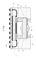
- an image sensor packaging structure with a predetermined focal length includes a substrate 10, a chip 20, an optical assembly 30, and an encapsulation compound 50.
- the encapsulation compound 50 is formed on the substrate 10 by a dispensing process so as to surround the chip 20 and the optical assembly 30.
- the image sensor packaging structure additionally includes at least one dam 40 provided around the perimeter of a top surface of the optical assembly 30, and the encapsulation compound 50 is formed on the substrate 10 by a molding process so as to surround the chip 20, the optical assembly 30, and the at least one dam 40.
- the substrate 10 is a circuitized substrate and has a supporting surface 11 and a bottom surface 12.
- a plurality of first conductive contacts 111 are formed on the supporting surface 11.
- the chip 20 is a complementary metal oxide semiconductor (CMOS) image sensor chip or a charge-coupled device (CCD).
- CMOS complementary metal oxide semiconductor
- CCD charge-coupled device
- the chip 20 has a first surface 21 and a second surface 22, wherein the first surface 21 is coupled to the supporting surface 11 of the substrate 10.
- the coupling between the chip 20 and the supporting surface 11 can be achieved by bonding or any other means.
- the second surface 22 of the chip 20 has a sensitization area 221 and is provided with a plurality of second conductive contacts 23, wherein the sensitization area 221 is composed of a plurality of photosensitive elements.
- the second conductive contacts 23 are arranged around the sensitization area 221 and electrically connected to the first conductive contacts 111 on the substrate 10 by wire bonding with conductive wires 60.
- the optical assembly 30 is coupled to the second surface 22 of the chip 20 and located above the sensitization area 221 of the chip 20 so as to cover the sensitization area 221 and form an air cavity 31.
- the optical assembly 30 is assembled and tested in advance. As shown in FIG. 4 , while the optical assembly 30 includes a lens, the optical assembly 30 further has a predetermined focal length.
- the dam 40 is provided around the perimeter of the top surface of the optical assembly 30, thus forming a closed structure on the top surface of the optical assembly 30.
- the dam 40 is made of epoxy or a film. More specifically, the epoxy or film is provided at a predetermined position and then cured or semi-cured by ultraviolet radiation or baking. Thus, the dam 40 maintains adequate resilience and can be deformed slightly during a subsequent molding process so as to absorb the mold-closing pressure from an upper mold section and block the encapsulation compound 50 outside the dam 40.
- the semi-product of the image sensor packaging structure is put in a mold (not shown) which includes an upper mold section and a lower mold section.
- the lower mold section is configured to support and contact with the bottom surface 12 of the substrate 10 while the side wall of the upper mold section is placed on the supporting surface 11 of the substrate 10 such that the supporting surface 11 and the bottom surface 12 of the substrate 10 are clamped between the upper and lower mold sections.
- the upper mold section has an inner upper surface which is formed as a flat surface and contacts with a top surface of the dam 40.
- the upper and lower mold sections jointly form a mold cavity therebetween.
- the encapsulation compound 50 is filled into the mold cavity and formed on the substrate 10 by molding process.
- the encapsulation compound 50 embeds the conductive wires 60 and surrounds the chip 20, the optical assembly 30, and the dam 40. Since the dam 40, together with the optical assembly 30 and the upper mold section, forms a barrier wall, the encapsulation compound 50 is blocked outside the dam 40 and the barrier wall can prevent the encapsulation compound 50 from overflowing to the optical assembly 30.
- the optical assembly 30 includes a first supporting frame 32 and a first light-transparent lid 33.
- the first supporting frame 32 has a third surface 321 and a fourth surface 322.
- the third surface 321 of the first supporting frame 32 is coupled to the second surface 22 of the chip 20 between the sensitization area 221 and the second conductive contacts 23.
- a first opening 323 is defined in the first supporting frame 32 and corresponds in position to the sensitization area 221.
- the first light-transparent lid 33 has a fifth surface 331 and a sixth surface 332, wherein the fifth surface 331 is coupled to the fourth surface 322 of the first supporting frame 32.
- the dam 40 is provided around the perimeter of the sixth surface 332 of the first light-transparent lid 33.
- the present embodiment further includes a plurality of solder balls 130 provided on the bottom surface 12 of the substrate 10.
- the solder balls 130 are electrically connected to the first conductive contacts 111 via a circuit structure in the substrate 10, thus allowing electrical connection between the image sensor packaging structure and other circuit devices.
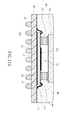
- an image sensor packaging structure with a predetermined focal length further includes a first lens 70 and a second lens 71.
- the first lens 70 and the second lens 71 are coupled to the fifth surface 331 and the sixth surface 332 of the first light-transparent lid 33, respectively.
- At least one of the first lens 70 and the second lens 71 is an aspherical lens, and each of the first lens 70 and the second lens 71 can be a spherical lens or an aspherical lens.
- an infrared filter layer 80 is provided between the second lens 71 and the sixth surface 332 of the first light-transparent lid 33, and a first light-shielding layer 90 can be further provided on the infrared filter layer 80.
- the first light-shielding layer 90 is formed with a first window 100 corresponding in position to the second lens 71.
- the infrared filter layer 80 is provided between the first lens 70 and the fifth surface 331 of the first light-transparent lid 33 (not shown), rather than between the second lens 71 and the sixth surface 332 of the first light-transparent lid 33.
- the infrared filter layer 80 is provided between the first lens 70 and the fifth surface 331, the first light-shielding layer 90 can be provided on the infrared filter layer 80.
- the first window 100 of the first light-shielding layer 90 corresponds in position to the first lens 70. As shown in FIG.
- the second embodiment further includes a plurality of solder pads 140 provided around the perimeter of the bottom surface 12 of the substrate 10 or arranged in an array (not shown).
- the solder pads 140 are electrically connected to the first conductive contacts 111 via the circuit structure in the substrate 10.
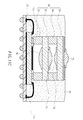
- the optical assembly 30 includes a second supporting frame 34, a second light-transparent lid 35, a third lens 72, and a fourth lens 73, in addition to the first supporting frame 32, the first light-transparent lid 33, the first lens 70, and the second lens 71.
- the second supporting frame 34 has a seventh surface 341 and an eighth surface 342, wherein the seventh surface 341 is coupled to the sixth surface 332 of the first light-transparent lid 33.
- the second supporting frame 34 defines therein a second opening 343 that corresponds in position to the first opening 323 of the first supporting frame 32.
- the first lens 70, the second lens 71, the third lens 72, and the fourth lens 73 can be either spherical or aspherical lenses, but at least one of them must be an aspherical lens.
- the second light-transparent lid 35 has a ninth surface 351 and a tenth surface 352, wherein the ninth surface 351 is coupled to the eighth surface 342 of the second supporting frame 34.
- the third lens 72 is coupled to the ninth surface 351 of the second light-transparent lid 35 while the fourth lens 73 is coupled to the tenth surface 352 of the second light-transparent lid 35.
- an infrared filter layer 80 is provided between the fourth lens 73 and the tenth surface 352, and a second light-shielding layer 91 can be further provided on the infrared filter layer 80, wherein the second light-shielding layer 91 is formed with a second window 101 that corresponds in position to the fourth lens 73.
- the dam 40 is formed around the perimeter of the tenth surface 352. While the infrared filter layer 80 and /or the second light-shielding layer 91 is provided on the tenth surface 352, the dam 40 can be formed on the infrared filter layer 80 (not shown) or the second light-shielding layer 91 (as shown in FIG. 5 and FIG. 6 ).
- the third embodiment may be configured in such a way that the infrared filter layer 80 is provided between the third lens 72 and the ninth surface 351 while the second light-shielding layer 91 is provided on the infrared filter layer 80.
- the second window 101 of the second light-shielding layer 91 corresponds in position to the third lens 72.
- the second light-shielding layer 91 is provided around the perimeter of the tenth surface 352, wherein the second window 101 of the second light-shielding layer 91 corresponds in position to the fourth lens 73.
- the optical assembly 30 includes a lens barrel 150, at least one third light-transparent lid 36, and at least two fifth lenses 74.
- the lens barrel 150 has a bottom surface 151 and a top surface 152, wherein the bottom surface 151 is coupled to the second surface 22 of the chip 20 between the sensitization area 221 and the second conductive contacts 23.
- the dam 40 is formed around a perimeter of the top surface 152 of the lens barrel 150.
- the third light-transparent lids 36 are fixedly provided in the lens barrel 150.
- Each third light-transparent lid 36 has an eleventh surface 361 and a twelfth surface 362.
- the fifth lenses 74 are coupled to the eleventh surfaces 361 and the twelfth surfaces 362, respectively.
- An infrared filter layer 80 is provided between one of the fifth lenses 74 and the corresponding twelfth surface 362.
- the infrared filter layer 80 is provided between one of the fifth lenses 74 and the corresponding eleventh surface 361 (not shown), rather than between one of the fifth lenses 74 and the corresponding twelfth surface 362.
- no matter where the infrared filter layer 80 is located there can only be one single-sided infrared filter layer 80.
- the optical assembly 30 includes a fourth light-transparent lid 37, a third supporting frame 38, a fifth light-transparent lid 39, a sixth lens 75, and a seventh lens 76.
- the fourth light-transparent lid 37 has a thirteenth surface 371 and a fourteenth surface 372.
- the fourth light-transparent lid 37 is peripherally coupled to the second surface 22 of the chip 20 via the thirteenth surface 371 and an adhesive layer 120, wherein the adhesive layer 120 is located between the sensitization area 221 and the second conductive contacts 23. Further, an infrared filter layer 80 is provided on the thirteenth surface 371.
- the third supporting frame 38 has a fifteenth surface 381 and a sixteenth surface 382, wherein the fifteenth surface 381 is coupled to the fourteenth surface 372. Also, the third supporting frame 38 defines therein a third opening 383 that corresponds in position to the sensitization area 221 of the chip 20. Moreover, the dam 40 is formed around a perimeter of the sixteenth surface 382.
- the fifth light-transparent lid 39 which has a seventeenth surface 391 and an eighteenth surface 392, is fixedly provided in the third opening 383 and fixed to the third supporting frame 38. As shown in FIG. 9 and FIG. 10 , the sixth lens 75 is coupled to the seventeenth surface 391 while the seventh lens 76 is coupled to the eighteenth surface 392. Furthermore, a third light-shielding layer 92 is provided on the eighteenth surface 392 and formed with a third window 102 that corresponds in position to the seventh lens 76.
- the optical assembly 30 is assembled and tested in advance and therefore does not require a focus adjusting procedure. In consequence, the manufacturing process is simplified, and the costs of equipment, man power, and materials are substantially reduced.
- the encapsulation compound 50 can be formed by transfer molding regardless of the configuration of the image sensor packaging structure, thus significantly shortening the cycle time of the manufacturing process and increasing the throughput per time unit while lowering related costs indirectly.
- the dam 40 which is provided between the mold and the optical assembly 30 and stays adequately resilient, not only functions as a buffer between the mold and the optical assembly 30 to prevent the optical assembly 30 from damage, but also conveys the pressure to the assembled and tested optical assembly 30, thus providing a leveling effect, by which the inclination of the optical assembly 30 relative to the chip 20 is reduced. In consequence, the optical focal length of the optical assembly 30 is then more readily positioned on the sensitization area 221of the chip 20.
- the dam 40 provided around the perimeter of the top surface of the optical assembly 30 serves as a barrier wall between the optical assembly 30 and the upper mold section. Due to the dam 40, the encapsulation compound 50 is blocked outside the optical assembly 30 and keeps the encapsulation compound 50 from overflowing to the optical assembly 30. Further, as the upper mold section is in direct and close contact with the dam 40, the upper mold section does not make direct contact with the optical assembly 30 and is therefore prevented from damaging or causing surface contamination to the optical assembly 30.
- the encapsulation compound 50 may also be formed on the substrate 10 by a dispensing process.
- the dispensing process it is no longer necessary to provide the at least one dam 40 on the optical assembly 30, and yet the optical assembly 30 may still take on the various aspects described above.
- the encapsulation compounds 50 are formed on their respective substrates 10 by a dispensing process without any dam 40 on the optical assemblies 30. Consequently, the overall heights of the image sensor packaging structures are reduced to effectively downsize the image sensor packaging structures.
Applications Claiming Priority (1)
| Application Number | Priority Date | Filing Date | Title |
|---|---|---|---|
| TW098146153A TWI425825B (zh) | 2009-12-31 | 2009-12-31 | 免調焦距影像感測器封裝結構 |
Publications (2)
| Publication Number | Publication Date |
|---|---|
| EP2341541A2 true EP2341541A2 (de) | 2011-07-06 |
| EP2341541A3 EP2341541A3 (de) | 2012-08-08 |
Family
ID=43416310
Family Applications (1)
| Application Number | Title | Priority Date | Filing Date |
|---|---|---|---|
| EP10187111A Withdrawn EP2341541A3 (de) | 2009-12-31 | 2010-10-11 | Bildsensorgehäusestruktur mit vorgegebener Brennweite |
Country Status (3)
| Country | Link |
|---|---|
| US (1) | US8441086B2 (de) |
| EP (1) | EP2341541A3 (de) |
| TW (1) | TWI425825B (de) |
Cited By (5)
| Publication number | Priority date | Publication date | Assignee | Title |
|---|---|---|---|---|
| EP2432017A3 (de) * | 2010-09-17 | 2013-02-27 | Kingpak Technology Inc. | Verfahren zur Herstellung einer geformten Bildsensorgehäusestruktur mit vorgegebener Brennweite und Struktur damit |
| CN108401094A (zh) * | 2017-02-08 | 2018-08-14 | 宁波舜宇光电信息有限公司 | 阵列摄像模组及其模塑感光组件和制造方法以及带有阵列摄像模组的电子设备 |
| CN108649041A (zh) * | 2018-04-16 | 2018-10-12 | 复旦大学 | 一种基于复合互连衬底的芯片封装结构及其方法 |
| CN110278426A (zh) * | 2018-03-18 | 2019-09-24 | 宁波舜宇光电信息有限公司 | 深度信息摄像模组及其基座组件、电子设备和制备方法 |
| WO2020094101A1 (zh) * | 2018-11-09 | 2020-05-14 | 昆山丘钛微电子科技有限公司 | 摄像头模组及其制作方法、终端 |
Families Citing this family (22)
| Publication number | Priority date | Publication date | Assignee | Title |
|---|---|---|---|---|
| JP2013118230A (ja) * | 2011-12-01 | 2013-06-13 | Canon Inc | 固体撮像装置 |
| WO2014115766A1 (ja) * | 2013-01-22 | 2014-07-31 | 京セラ株式会社 | 電子素子搭載用パッケージ、電子装置および撮像モジュール |
| JP5823043B2 (ja) * | 2013-01-31 | 2015-11-25 | 京セラ株式会社 | 電子素子搭載用基板、電子装置および撮像モジュール |
| US10211191B2 (en) * | 2014-08-06 | 2019-02-19 | Pixart Imaging Inc. | Image module package with transparent sub-assembly |
| US10498943B2 (en) | 2015-07-09 | 2019-12-03 | Ams Sensors Singapore Pte. Ltd. | Optoelectronic modules including overmold supporting an optical assembly |
| JP7005505B2 (ja) * | 2016-02-18 | 2022-01-21 | ニンボー サニー オプテック カンパニー,リミテッド | アレイ撮像モジュールおよび成形感光アセンブリ、回路基板アセンブリ、およびそれらの電子デバイス向け製造方法 |
| KR102193819B1 (ko) * | 2016-03-12 | 2020-12-23 | 닝보 써니 오포테크 코., 엘티디. | 어레이 이미징 모듈, 성형 감광성 어셈블리 및 그 제조 방법, 및 전자 장치 |
| CN105681640B (zh) * | 2016-03-28 | 2019-12-27 | 宁波舜宇光电信息有限公司 | 摄像模组及其制造方法 |
| US9798054B1 (en) * | 2016-03-30 | 2017-10-24 | Delphi Technologies, Inc. | Camera assembly for use on a vehicle |
| US10925160B1 (en) | 2016-06-28 | 2021-02-16 | Amazon Technologies, Inc. | Electronic device with a display assembly and silicon circuit board substrate |
| TWI635348B (zh) * | 2017-05-12 | 2018-09-11 | 海華科技股份有限公司 | 可攜式電子裝置及其影像擷取模組與承載組件 |
| TWI631672B (zh) * | 2017-09-01 | 2018-08-01 | 勝麗國際股份有限公司 | 感測器封裝結構 |
| CN109672806B (zh) * | 2017-10-13 | 2022-06-28 | 宁波舜宇光电信息有限公司 | 摄像模组和感光组件及其封装方法 |
| CN107770422A (zh) * | 2017-10-25 | 2018-03-06 | 信利光电股份有限公司 | 一种摄像头模组的制作方法及电子设备 |
| CN110649047A (zh) * | 2018-06-26 | 2020-01-03 | 三赢科技(深圳)有限公司 | 感光芯片封装结构及其形成方法 |
| WO2020192439A1 (zh) * | 2019-03-22 | 2020-10-01 | 宁波舜宇光电信息有限公司 | 摄像模组及其镜头组件和组装方法及带有摄像模组的电子设备 |
| US11444111B2 (en) * | 2019-03-28 | 2022-09-13 | Semiconductor Components Industries, Llc | Image sensor package having a light blocking member |
| TWI689018B (zh) * | 2019-04-23 | 2020-03-21 | 鴻海精密工業股份有限公司 | 影像感測器封裝結構、鏡頭模組及電子裝置 |
| JPWO2021187091A1 (de) * | 2020-03-17 | 2021-09-23 | ||
| CN112201667A (zh) * | 2020-11-06 | 2021-01-08 | 积高电子(无锡)有限公司 | 图像传感器的pop封装结构及封装方法 |
| GB202102011D0 (en) * | 2021-02-12 | 2021-03-31 | Ams Sensors Singapore Pte Ltd | Optoelectronic module |
| WO2024022217A1 (zh) * | 2022-07-27 | 2024-02-01 | 宁波舜宇光电信息有限公司 | 一种摄像模组及其制造方法 |
Citations (1)
| Publication number | Priority date | Publication date | Assignee | Title |
|---|---|---|---|---|
| US6972497B2 (en) | 2002-02-06 | 2005-12-06 | Stmicroelectronics S.A. | Optical semiconductor device and method of manufacture |
Family Cites Families (20)
| Publication number | Priority date | Publication date | Assignee | Title |
|---|---|---|---|---|
| AU2001253547A1 (en) * | 2000-05-23 | 2001-12-03 | Atmel Corporation | Integrated ic chip package for electronic image sensor die |
| JP2005072978A (ja) * | 2003-08-25 | 2005-03-17 | Renesas Technology Corp | 固体撮像装置およびその製造方法 |
| KR100539234B1 (ko) * | 2003-06-11 | 2005-12-27 | 삼성전자주식회사 | 투명 고분자 소재를 적용한 씨모스형 이미지 센서 모듈 및그 제조방법 |
| US6849915B1 (en) * | 2003-08-26 | 2005-02-01 | Ultra Tera Corporation | Light sensitive semiconductor package and fabrication method thereof |
| DE10344760A1 (de) * | 2003-09-26 | 2005-05-04 | Siemens Ag | Optisches Modul und optisches System |
| JP2006148710A (ja) * | 2004-11-22 | 2006-06-08 | Sharp Corp | 撮像モジュール及び撮像モジュールの製造方法 |
| TW200714043A (en) * | 2005-09-05 | 2007-04-01 | Altus Technology Inc | Image sensor package and digital camera module therewith |
| JP4382030B2 (ja) * | 2005-11-15 | 2009-12-09 | 富士通マイクロエレクトロニクス株式会社 | 半導体装置及びその製造方法 |
| US20080203512A1 (en) * | 2006-06-07 | 2008-08-28 | Hon Hai Precision Industry Co., Ltd. | Image sensor chip package |
| WO2008132980A1 (ja) * | 2007-04-17 | 2008-11-06 | Konica Minolta Opto, Inc. | 撮像装置の製造方法、撮像装置及び携帯端末 |
| TWI351217B (en) * | 2007-04-27 | 2011-10-21 | Hon Hai Prec Ind Co Ltd | Imageing module |
| JP4378394B2 (ja) * | 2007-05-31 | 2009-12-02 | シャープ株式会社 | 半導体装置およびそれを備えた光学装置用モジュール |
| JP4384202B2 (ja) * | 2007-05-31 | 2009-12-16 | シャープ株式会社 | 半導体装置およびそれを備えた光学装置用モジュール |
| TWI346221B (en) * | 2007-06-15 | 2011-08-01 | Hon Hai Prec Ind Co Ltd | Camera module and image sensor package structure |
| US7923298B2 (en) * | 2007-09-07 | 2011-04-12 | Micron Technology, Inc. | Imager die package and methods of packaging an imager die on a temporary carrier |
| EP2220684A1 (de) * | 2007-11-27 | 2010-08-25 | Heptagon Oy | Verkapselter linsenstapel |
| US20090206431A1 (en) * | 2008-02-20 | 2009-08-20 | Micron Technology, Inc. | Imager wafer level module and method of fabrication and use |
| US8004602B2 (en) * | 2008-05-16 | 2011-08-23 | Kingpak Technology Inc. | Image sensor structure and integrated lens module thereof |
| CN101924081A (zh) * | 2009-06-15 | 2010-12-22 | 鸿富锦精密工业(深圳)有限公司 | 影像感测器封装体及影像感测器模组 |
| TW201104850A (en) * | 2009-07-29 | 2011-02-01 | Kingpak Tech Inc | Image sensor package structure with large air cavity |
-
2009
- 2009-12-31 TW TW098146153A patent/TWI425825B/zh not_active IP Right Cessation
-
2010
- 2010-10-11 EP EP10187111A patent/EP2341541A3/de not_active Withdrawn
- 2010-11-16 US US12/947,210 patent/US8441086B2/en not_active Expired - Fee Related
Patent Citations (1)
| Publication number | Priority date | Publication date | Assignee | Title |
|---|---|---|---|---|
| US6972497B2 (en) | 2002-02-06 | 2005-12-06 | Stmicroelectronics S.A. | Optical semiconductor device and method of manufacture |
Cited By (10)
| Publication number | Priority date | Publication date | Assignee | Title |
|---|---|---|---|---|
| EP2432017A3 (de) * | 2010-09-17 | 2013-02-27 | Kingpak Technology Inc. | Verfahren zur Herstellung einer geformten Bildsensorgehäusestruktur mit vorgegebener Brennweite und Struktur damit |
| US8481343B2 (en) | 2010-09-17 | 2013-07-09 | Kingpak Technology Inc. | Manufacturing method of molded image sensor packaging structure with predetermined focal length and the structure using the same |
| CN108401094A (zh) * | 2017-02-08 | 2018-08-14 | 宁波舜宇光电信息有限公司 | 阵列摄像模组及其模塑感光组件和制造方法以及带有阵列摄像模组的电子设备 |
| EP3582484A4 (de) * | 2017-02-08 | 2020-11-04 | Ningbo Sunny Opotech Co., Ltd. | Kameramodul, daraus geformtes lichtempfindliches bauteil, herstellungsverfahren dafür und elektronische vorrichtung |
| US10979610B2 (en) | 2017-02-08 | 2021-04-13 | Ningbo Sunny Opotech Co., Ltd. | Camera module, molding photosensitive assembly thereof, manufacturing method and electronic device |
| CN110278426A (zh) * | 2018-03-18 | 2019-09-24 | 宁波舜宇光电信息有限公司 | 深度信息摄像模组及其基座组件、电子设备和制备方法 |
| CN110278426B (zh) * | 2018-03-18 | 2024-02-13 | 宁波舜宇光电信息有限公司 | 深度信息摄像模组及其基座组件、电子设备和制备方法 |
| CN108649041A (zh) * | 2018-04-16 | 2018-10-12 | 复旦大学 | 一种基于复合互连衬底的芯片封装结构及其方法 |
| CN108649041B (zh) * | 2018-04-16 | 2021-01-26 | 复旦大学 | 一种基于复合互连衬底的芯片封装结构及其方法 |
| WO2020094101A1 (zh) * | 2018-11-09 | 2020-05-14 | 昆山丘钛微电子科技有限公司 | 摄像头模组及其制作方法、终端 |
Also Published As
| Publication number | Publication date |
|---|---|
| US20110156187A1 (en) | 2011-06-30 |
| TWI425825B (zh) | 2014-02-01 |
| TW201123858A (en) | 2011-07-01 |
| US8441086B2 (en) | 2013-05-14 |
| EP2341541A3 (de) | 2012-08-08 |
Similar Documents
| Publication | Publication Date | Title |
|---|---|---|
| US8441086B2 (en) | Image sensor packaging structure with predetermined focal length | |
| EP2393116B1 (de) | Waferlevel-Bildsensorverpackungsstruktur und Herstellungsverfahren dafür | |
| US8928104B2 (en) | Image sensor packaging structure with black encapsulant | |
| US11824071B2 (en) | Camera module and molded photosensitive assembly and manufacturing method thereof, and electronic device | |
| US20220021792A1 (en) | Array camera module and application thereof | |
| US7911017B1 (en) | Direct glass attached on die optical module | |
| CN111193852B (zh) | 摄像模组及其制造方法 | |
| JP4673721B2 (ja) | 撮像装置及びその製造方法 | |
| KR101070058B1 (ko) | 카메라 모듈 패키지 | |
| CN107566691B (zh) | 感光组件和摄像模组及其制造方法 | |
| EP2432017B1 (de) | Verfahren zur Herstellung einer geformten Bildsensorgehäusestruktur mit vorgegebener Brennweite und Struktur damit | |
| US20070287216A1 (en) | Microelectronic imaging units and methods of manufacturing microelectronic imaging units | |
| US8110884B2 (en) | Methods of packaging imager devices and optics modules, and resulting assemblies | |
| US20090256222A1 (en) | Packaging method of image sensing device | |
| CN108401091B (zh) | 摄像模组及其模制电路板组件和应用 | |
| EP3484139B1 (de) | Lichtempfindliches bauelement und kameramodul | |
| EP3562136A2 (de) | Bilderfassungsmodul, leiterplattenanordnung, herstellungsverfahren und mit dem bilderfassungsmodul ausgestattete elektronische vorrichtung | |
| US8952412B2 (en) | Method for fabricating a solid-state imaging package | |
| US20230207588A1 (en) | Integrated photosensitive module, photosensitive assembly, camera module and preparation method therefor | |
| US20090215216A1 (en) | Packaging method of image sensing device | |
| CN107734215B (zh) | 摄像模组及其模塑感光组件和制造方法以及电子设备 | |
| CN109672806B (zh) | 摄像模组和感光组件及其封装方法 | |
| US20210185195A1 (en) | Imaging unit and imaging device | |
| CN111277734B (zh) | 摄像模组及其制造方法 | |
| KR20070092546A (ko) | 카메라 모듈 및 그 제조 방법 |
Legal Events
| Date | Code | Title | Description |
|---|---|---|---|
| PUAI | Public reference made under article 153(3) epc to a published international application that has entered the european phase |
Free format text: ORIGINAL CODE: 0009012 |
|
| AK | Designated contracting states |
Kind code of ref document: A2 Designated state(s): AL AT BE BG CH CY CZ DE DK EE ES FI FR GB GR HR HU IE IS IT LI LT LU LV MC MK MT NL NO PL PT RO RS SE SI SK SM TR |
|
| AX | Request for extension of the european patent |
Extension state: BA ME |
|
| RIC1 | Information provided on ipc code assigned before grant |
Ipc: H01L 27/146 20060101AFI20120322BHEP |
|
| PUAL | Search report despatched |
Free format text: ORIGINAL CODE: 0009013 |
|
| AK | Designated contracting states |
Kind code of ref document: A3 Designated state(s): AL AT BE BG CH CY CZ DE DK EE ES FI FR GB GR HR HU IE IS IT LI LT LU LV MC MK MT NL NO PL PT RO RS SE SI SK SM TR |
|
| AX | Request for extension of the european patent |
Extension state: BA ME |
|
| RIC1 | Information provided on ipc code assigned before grant |
Ipc: H01L 27/146 20060101AFI20120704BHEP |
|
| 17P | Request for examination filed |
Effective date: 20130118 |
|
| 17Q | First examination report despatched |
Effective date: 20130219 |
|
| RAP1 | Party data changed (applicant data changed or rights of an application transferred) |
Owner name: KINGPAK TECHNOLOGY INC. |
|
| STAA | Information on the status of an ep patent application or granted ep patent |
Free format text: STATUS: THE APPLICATION IS DEEMED TO BE WITHDRAWN |
|
| 18D | Application deemed to be withdrawn |
Effective date: 20160503 |