EP2341541A2 - Image sensor packaging structure with predetermined focal length - Google Patents
Image sensor packaging structure with predetermined focal length Download PDFInfo
- Publication number
- EP2341541A2 EP2341541A2 EP10187111A EP10187111A EP2341541A2 EP 2341541 A2 EP2341541 A2 EP 2341541A2 EP 10187111 A EP10187111 A EP 10187111A EP 10187111 A EP10187111 A EP 10187111A EP 2341541 A2 EP2341541 A2 EP 2341541A2
- Authority
- EP
- European Patent Office
- Prior art keywords
- coupled
- lens
- image sensor
- packaging structure
- light
- Prior art date
- Legal status (The legal status is an assumption and is not a legal conclusion. Google has not performed a legal analysis and makes no representation as to the accuracy of the status listed.)
- Withdrawn
Links
- 238000004806 packaging method and process Methods 0.000 title claims abstract description 63
- 230000003287 optical effect Effects 0.000 claims abstract description 66
- 206010070834 Sensitisation Diseases 0.000 claims abstract description 40
- 230000008313 sensitization Effects 0.000 claims abstract description 40
- 239000000758 substrate Substances 0.000 claims abstract description 33
- 238000005538 encapsulation Methods 0.000 claims abstract description 26
- 238000000034 method Methods 0.000 claims abstract description 23
- 230000008569 process Effects 0.000 claims abstract description 18
- 238000000465 moulding Methods 0.000 claims abstract description 12
- 150000001875 compounds Chemical class 0.000 claims abstract description 9
- 239000012790 adhesive layer Substances 0.000 claims description 6
- 239000004593 Epoxy Substances 0.000 claims description 4
- 239000004065 semiconductor Substances 0.000 claims description 3
- 230000000295 complement effect Effects 0.000 claims description 2
- 229910044991 metal oxide Inorganic materials 0.000 claims description 2
- 150000004706 metal oxides Chemical class 0.000 claims description 2
- 239000010410 layer Substances 0.000 description 31
- 238000004519 manufacturing process Methods 0.000 description 17
- MPDDTAJMJCESGV-CTUHWIOQSA-M (3r,5r)-7-[2-(4-fluorophenyl)-5-[methyl-[(1r)-1-phenylethyl]carbamoyl]-4-propan-2-ylpyrazol-3-yl]-3,5-dihydroxyheptanoate Chemical compound C1([C@@H](C)N(C)C(=O)C2=NN(C(CC[C@@H](O)C[C@@H](O)CC([O-])=O)=C2C(C)C)C=2C=CC(F)=CC=2)=CC=CC=C1 MPDDTAJMJCESGV-CTUHWIOQSA-M 0.000 description 15
- 229910000679 solder Inorganic materials 0.000 description 4
- 230000004888 barrier function Effects 0.000 description 3
- 239000000463 material Substances 0.000 description 3
- 230000000694 effects Effects 0.000 description 2
- 230000001965 increasing effect Effects 0.000 description 2
- 229920000642 polymer Polymers 0.000 description 2
- 238000004904 shortening Methods 0.000 description 2
- 238000001721 transfer moulding Methods 0.000 description 2
- 230000000712 assembly Effects 0.000 description 1
- 238000000429 assembly Methods 0.000 description 1
- 238000011109 contamination Methods 0.000 description 1
- 230000008878 coupling Effects 0.000 description 1
- 238000010168 coupling process Methods 0.000 description 1
- 238000005859 coupling reaction Methods 0.000 description 1
- 230000002708 enhancing effect Effects 0.000 description 1
- 230000006870 function Effects 0.000 description 1
- 230000006872 improvement Effects 0.000 description 1
- 230000004048 modification Effects 0.000 description 1
- 238000012986 modification Methods 0.000 description 1
- 238000012858 packaging process Methods 0.000 description 1
- 230000005855 radiation Effects 0.000 description 1
Images


Classifications
-
- H—ELECTRICITY
- H01—ELECTRIC ELEMENTS
- H01L—SEMICONDUCTOR DEVICES NOT COVERED BY CLASS H10
- H01L27/00—Devices consisting of a plurality of semiconductor or other solid-state components formed in or on a common substrate
- H01L27/14—Devices consisting of a plurality of semiconductor or other solid-state components formed in or on a common substrate including semiconductor components sensitive to infrared radiation, light, electromagnetic radiation of shorter wavelength or corpuscular radiation and specially adapted either for the conversion of the energy of such radiation into electrical energy or for the control of electrical energy by such radiation
- H01L27/144—Devices controlled by radiation
- H01L27/146—Imager structures
- H01L27/14601—Structural or functional details thereof
- H01L27/14618—Containers
-
- H—ELECTRICITY
- H01—ELECTRIC ELEMENTS
- H01L—SEMICONDUCTOR DEVICES NOT COVERED BY CLASS H10
- H01L27/00—Devices consisting of a plurality of semiconductor or other solid-state components formed in or on a common substrate
- H01L27/14—Devices consisting of a plurality of semiconductor or other solid-state components formed in or on a common substrate including semiconductor components sensitive to infrared radiation, light, electromagnetic radiation of shorter wavelength or corpuscular radiation and specially adapted either for the conversion of the energy of such radiation into electrical energy or for the control of electrical energy by such radiation
- H01L27/144—Devices controlled by radiation
- H01L27/146—Imager structures
- H01L27/14601—Structural or functional details thereof
- H01L27/14625—Optical elements or arrangements associated with the device
-
- H—ELECTRICITY
- H01—ELECTRIC ELEMENTS
- H01L—SEMICONDUCTOR DEVICES NOT COVERED BY CLASS H10
- H01L27/00—Devices consisting of a plurality of semiconductor or other solid-state components formed in or on a common substrate
- H01L27/14—Devices consisting of a plurality of semiconductor or other solid-state components formed in or on a common substrate including semiconductor components sensitive to infrared radiation, light, electromagnetic radiation of shorter wavelength or corpuscular radiation and specially adapted either for the conversion of the energy of such radiation into electrical energy or for the control of electrical energy by such radiation
- H01L27/144—Devices controlled by radiation
- H01L27/146—Imager structures
- H01L27/14683—Processes or apparatus peculiar to the manufacture or treatment of these devices or parts thereof
- H01L27/14685—Process for coatings or optical elements
-
- H—ELECTRICITY
- H01—ELECTRIC ELEMENTS
- H01L—SEMICONDUCTOR DEVICES NOT COVERED BY CLASS H10
- H01L2224/00—Indexing scheme for arrangements for connecting or disconnecting semiconductor or solid-state bodies and methods related thereto as covered by H01L24/00
- H01L2224/01—Means for bonding being attached to, or being formed on, the surface to be connected, e.g. chip-to-package, die-attach, "first-level" interconnects; Manufacturing methods related thereto
- H01L2224/42—Wire connectors; Manufacturing methods related thereto
- H01L2224/47—Structure, shape, material or disposition of the wire connectors after the connecting process
- H01L2224/48—Structure, shape, material or disposition of the wire connectors after the connecting process of an individual wire connector
- H01L2224/4805—Shape
- H01L2224/4809—Loop shape
- H01L2224/48091—Arched
-
- H—ELECTRICITY
- H01—ELECTRIC ELEMENTS
- H01L—SEMICONDUCTOR DEVICES NOT COVERED BY CLASS H10
- H01L2224/00—Indexing scheme for arrangements for connecting or disconnecting semiconductor or solid-state bodies and methods related thereto as covered by H01L24/00
- H01L2224/01—Means for bonding being attached to, or being formed on, the surface to be connected, e.g. chip-to-package, die-attach, "first-level" interconnects; Manufacturing methods related thereto
- H01L2224/42—Wire connectors; Manufacturing methods related thereto
- H01L2224/47—Structure, shape, material or disposition of the wire connectors after the connecting process
- H01L2224/48—Structure, shape, material or disposition of the wire connectors after the connecting process of an individual wire connector
- H01L2224/481—Disposition
- H01L2224/48151—Connecting between a semiconductor or solid-state body and an item not being a semiconductor or solid-state body, e.g. chip-to-substrate, chip-to-passive
- H01L2224/48221—Connecting between a semiconductor or solid-state body and an item not being a semiconductor or solid-state body, e.g. chip-to-substrate, chip-to-passive the body and the item being stacked
- H01L2224/48225—Connecting between a semiconductor or solid-state body and an item not being a semiconductor or solid-state body, e.g. chip-to-substrate, chip-to-passive the body and the item being stacked the item being non-metallic, e.g. insulating substrate with or without metallisation
- H01L2224/48227—Connecting between a semiconductor or solid-state body and an item not being a semiconductor or solid-state body, e.g. chip-to-substrate, chip-to-passive the body and the item being stacked the item being non-metallic, e.g. insulating substrate with or without metallisation connecting the wire to a bond pad of the item
-
- H—ELECTRICITY
- H01—ELECTRIC ELEMENTS
- H01L—SEMICONDUCTOR DEVICES NOT COVERED BY CLASS H10
- H01L2224/00—Indexing scheme for arrangements for connecting or disconnecting semiconductor or solid-state bodies and methods related thereto as covered by H01L24/00
- H01L2224/01—Means for bonding being attached to, or being formed on, the surface to be connected, e.g. chip-to-package, die-attach, "first-level" interconnects; Manufacturing methods related thereto
- H01L2224/42—Wire connectors; Manufacturing methods related thereto
- H01L2224/47—Structure, shape, material or disposition of the wire connectors after the connecting process
- H01L2224/48—Structure, shape, material or disposition of the wire connectors after the connecting process of an individual wire connector
- H01L2224/484—Connecting portions
- H01L2224/48463—Connecting portions the connecting portion on the bonding area of the semiconductor or solid-state body being a ball bond
- H01L2224/48465—Connecting portions the connecting portion on the bonding area of the semiconductor or solid-state body being a ball bond the other connecting portion not on the bonding area being a wedge bond, i.e. ball-to-wedge, regular stitch
-
- H—ELECTRICITY
- H01—ELECTRIC ELEMENTS
- H01L—SEMICONDUCTOR DEVICES NOT COVERED BY CLASS H10
- H01L2224/00—Indexing scheme for arrangements for connecting or disconnecting semiconductor or solid-state bodies and methods related thereto as covered by H01L24/00
- H01L2224/01—Means for bonding being attached to, or being formed on, the surface to be connected, e.g. chip-to-package, die-attach, "first-level" interconnects; Manufacturing methods related thereto
- H01L2224/42—Wire connectors; Manufacturing methods related thereto
- H01L2224/47—Structure, shape, material or disposition of the wire connectors after the connecting process
- H01L2224/48—Structure, shape, material or disposition of the wire connectors after the connecting process of an individual wire connector
- H01L2224/484—Connecting portions
- H01L2224/4847—Connecting portions the connecting portion on the bonding area of the semiconductor or solid-state body being a wedge bond
- H01L2224/48471—Connecting portions the connecting portion on the bonding area of the semiconductor or solid-state body being a wedge bond the other connecting portion not on the bonding area being a ball bond, i.e. wedge-to-ball, reverse stitch
-
- H—ELECTRICITY
- H01—ELECTRIC ELEMENTS
- H01L—SEMICONDUCTOR DEVICES NOT COVERED BY CLASS H10
- H01L2224/00—Indexing scheme for arrangements for connecting or disconnecting semiconductor or solid-state bodies and methods related thereto as covered by H01L24/00
- H01L2224/01—Means for bonding being attached to, or being formed on, the surface to be connected, e.g. chip-to-package, die-attach, "first-level" interconnects; Manufacturing methods related thereto
- H01L2224/42—Wire connectors; Manufacturing methods related thereto
- H01L2224/47—Structure, shape, material or disposition of the wire connectors after the connecting process
- H01L2224/48—Structure, shape, material or disposition of the wire connectors after the connecting process of an individual wire connector
- H01L2224/484—Connecting portions
- H01L2224/48475—Connecting portions connected to auxiliary connecting means on the bonding areas, e.g. pre-ball, wedge-on-ball, ball-on-ball
- H01L2224/48476—Connecting portions connected to auxiliary connecting means on the bonding areas, e.g. pre-ball, wedge-on-ball, ball-on-ball between the wire connector and the bonding area
- H01L2224/48477—Connecting portions connected to auxiliary connecting means on the bonding areas, e.g. pre-ball, wedge-on-ball, ball-on-ball between the wire connector and the bonding area being a pre-ball (i.e. a ball formed by capillary bonding)
- H01L2224/48478—Connecting portions connected to auxiliary connecting means on the bonding areas, e.g. pre-ball, wedge-on-ball, ball-on-ball between the wire connector and the bonding area being a pre-ball (i.e. a ball formed by capillary bonding) the connecting portion being a wedge bond, i.e. wedge on pre-ball
- H01L2224/48479—Connecting portions connected to auxiliary connecting means on the bonding areas, e.g. pre-ball, wedge-on-ball, ball-on-ball between the wire connector and the bonding area being a pre-ball (i.e. a ball formed by capillary bonding) the connecting portion being a wedge bond, i.e. wedge on pre-ball on the semiconductor or solid-state body
-
- H—ELECTRICITY
- H01—ELECTRIC ELEMENTS
- H01L—SEMICONDUCTOR DEVICES NOT COVERED BY CLASS H10
- H01L2224/00—Indexing scheme for arrangements for connecting or disconnecting semiconductor or solid-state bodies and methods related thereto as covered by H01L24/00
- H01L2224/73—Means for bonding being of different types provided for in two or more of groups H01L2224/10, H01L2224/18, H01L2224/26, H01L2224/34, H01L2224/42, H01L2224/50, H01L2224/63, H01L2224/71
- H01L2224/732—Location after the connecting process
- H01L2224/73251—Location after the connecting process on different surfaces
- H01L2224/73265—Layer and wire connectors
-
- H—ELECTRICITY
- H01—ELECTRIC ELEMENTS
- H01L—SEMICONDUCTOR DEVICES NOT COVERED BY CLASS H10
- H01L2924/00—Indexing scheme for arrangements or methods for connecting or disconnecting semiconductor or solid-state bodies as covered by H01L24/00
- H01L2924/0001—Technical content checked by a classifier
- H01L2924/00014—Technical content checked by a classifier the subject-matter covered by the group, the symbol of which is combined with the symbol of this group, being disclosed without further technical details
Abstract
Description
- The present invention relates to an image sensor packaging structure and, more particularly, to an image sensor packaging structure having a predetermined focal length and equipped with an optical assembly which is assembled, tested, and calibrated in advance.
- Image sensors are configured to receive light in the surrounding space and convert-optical signals into electrical signals and are therefore widely used as a key component in a variety of photoelectric products. A conventional image sensor packaging structure is typically made in the following manner. An image sensor chip is disposed on a substrate and electrically connected thereto by conductive wires. Then, a light-transparent lid or a lens set is provided above the image sensor chip such that light passing through the light-transparent lid or the lens set can be captured by the image sensor chip. After packaging, the resultant image sensor packaging structure is ready for use by a system manufacturer. For example the image sensor packaging structure can be integrated into an external device, such as a printed circuit board, and applied to a digital still camera (DSC), a digital video recorder (DV), a surveillance device, a cell phone, an image sensor module for vehicles, and many other electronic products.
- In order to satisfy consumers' demands of electronic products, manufacturers have spared no effort in downsizing the image sensor packaging structure and simplifying its packaging process. For instance, referring to
FIG. 1 for an image sensor packaging structure disclosed byUS Patent No. 6,972,497 , which is entitled "Optical Semiconductor Device and Method of Manufacture" and granted on December 6, 2005, asensor chip 1 is provided withconductive wires 2 for electrically connecting thesensor chip 1 to an underlying substrate or carrier. Then, a supportingmember 3 is provided above thesensor chip 1, and adam 4 is formed around and at some distance from thesensor chip 1. Afterwards, apolymer encapsulation 5, made of epoxy for example, is used to embed theconductive wires 2, before alens holder 6 is provided on the supportingmember 3. - The image sensor packaging structure of the above-cited US patent has the following drawbacks. First of all, the manufacturing method is complicated. Secondly, the supporting
member 3 incurs high production costs and material costs. Thirdly, thepolymer encapsulation 5 has high material costs and low productivity. Fourthly, the assembly tolerances between thesensor chip 1 and the supportingmember 3 and between the supportingmember 3 and thelens holder 6 are so large that it is structurally difficult to provide a predetermined focal length. More specifically, the optical assembly tends not to focus on the sensitization area of the image sensor but to cause an out-of-focus phenomenon. Last but not least, since each image sensor must be tested and calibrated individually, the time and costs required for the entire manufacturing process are increased. As a result, the cycle time of the manufacturing process cannot be effectively shortened, which in turn hinders improvement in throughput per time unit. - It is an object of the present invention to provide an image sensor packaging structure with a predetermined focal length, wherein an optical assembly is assembled and tested in advance to provide the predetermined focal length. The optical assembly can then focus on a sensitization area of the image sensor more readily, thus preventing the out-of-focus phenomenon which may otherwise result from the unduly large mechanical assembly tolerances in the prior art.
- It is another object of the present invention to provide an image sensor packaging structure with a predetermined focal length, wherein an optical assembly is assembled and tested in advance, so a focus adjusting procedure can be dispensed with. As the manufacturing process is simplified, the time and costs of the manufacturing process are both reduced.
- It is still another object of the present invention to provide an image sensor packaging structure with a predetermined focal length, wherein the image sensor packaging structure can be made by a molding process. Thus, the cycle time of the manufacturing process can be significantly shortened to increase the throughput per time unit.
- It is yet another object of the present invention to provide an image sensor packaging structure with a predetermined focal length, wherein the image sensor packaging structure can be made by a molding process and is hence suitable for batch-type mass-production, which helps to reduce production costs.
- To achieve the foregoing objects, the present invention provides an image sensor packaging structure with a predetermined focal length, wherein the image sensor packaging structure includes a substrate, a chip, an optical assembly, and an encapsulation compound. The substrate has a supporting surface and a bottom surface, wherein the supporting surface is formed with a plurality of first conductive contacts. The chip has a first surface coupled to the supporting surface of the substrate and a second surface having a sensitization area. The chip further includes a plurality of second conductive contacts arranged around the sensitization area and electrically connected to the first conductive contacts of the substrate. The optical assembly is coupled to the second surface of the chip and disposed above the sensitization area of the chip so as to cover the sensitization area and thereby form an air cavity. In addition, the optical assembly has a predetermined focal length. The encapsulation compound is formed to surround the chip and the optical assembly.
- Implementation of the present invention at least involves the following inventive steps:
- 1. According to the present invention, the pressure applied during a molding process is conveyed to the assembled and tested optical assembly to produce a leveling effect. Thus, the inclination of the optical assembly relative to the chip is reduced to ensure that the optical focal length is precisely positioned on the sensitization area.
- 2. The optical assembly is assembled and tested beforehand. Therefore, an otherwise necessary focus adjusting procedure can be spared to simplify the manufacturing process of the image sensor packaging structure.
- 3. The image sensor packaging structure can be made by a molding process, thereby shortening the cycle time of the manufacturing process and enhancing the throughput per time unit. Consequently, the time and costs of the manufacturing process are reduced.
- 4. As the image sensor packaging structure can be formed by a molding process, batch-type mass-production is applicable to cut the production costs of the image sensor packaging structure.
- 5. The image sensor packaging structure is lightweight and compact, thus meeting the demands of handheld products nowadays.
- The features and advantages of the present invention are detailed hereinafter with reference to the preferred embodiments. The detailed description is intended to enable a person skilled in the art to gain insight into the technical contents disclosed herein and implement the present invention accordingly. In particular, a person skilled in the art can easily understand the objects and advantages of the present invention by referring to the disclosure of the specification, the claims, and the accompanying drawings.
-
-
FIG. 1 is a sectional view of a conventional image sensor packaging structure. -
FIG. 2 is a sectional view of an image sensor packaging structure with a predetermined focal length according to a first embodiment of the present invention. -
FIG. 3 is a partial enlarged view ofFIG. 2 . -
FIG. 4 is a sectional view of an image sensor packaging structure with a predetermined focal length according to a second embodiment of the present invention. -
FIG. 5 is a sectional view of an image sensor packaging structure with a predetermined focal length according to a third embodiment of the present invention. -
FIG. 6 is a partial enlarged view ofFIG. 5 . -
FIG. 7 is a sectional view of an image sensor packaging structure with a predetermined focal length according to a fourth embodiment of the present invention. -
FIG. 8 is a partial enlarged view ofFIG. 7 . -
FIG. 9 is a sectional view of an image sensor packaging structure with a predetermined focal length according to a fifth embodiment of the present invention. -
FIG. 10 is a partial enlarged view ofFIG. 9 . -
FIG. 11A to FIG. 11D are sectional views of image sensor packaging structures with a predetermined focal length according to the present invention, wherein encapsulation compounds are formed on their respective substrates by a dispensing process. - Referring to
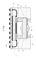
FIG. 2 andFIG. 3 , an image sensor packaging structure with a predetermined focal length according to a first embodiment of the present invention includes asubstrate 10, achip 20, anoptical assembly 30, and anencapsulation compound 50. Theencapsulation compound 50 is formed on thesubstrate 10 by a dispensing process so as to surround thechip 20 and theoptical assembly 30. Alternatively, the image sensor packaging structure additionally includes at least onedam 40 provided around the perimeter of a top surface of theoptical assembly 30, and theencapsulation compound 50 is formed on thesubstrate 10 by a molding process so as to surround thechip 20, theoptical assembly 30, and the at least onedam 40. - The following paragraphs are dedicated to embodiments which are provided with the at least one
dam 40 that allows theencapsulation compound 50 to be formed by molding process. Embodiments in which theencapsulation compound 50 is formed by a dispensing process are described further below. - As shown in
FIG. 2 , thesubstrate 10 is a circuitized substrate and has a supportingsurface 11 and abottom surface 12. A plurality of firstconductive contacts 111 are formed on the supportingsurface 11. - The
chip 20 is a complementary metal oxide semiconductor (CMOS) image sensor chip or a charge-coupled device (CCD). Thechip 20 has afirst surface 21 and asecond surface 22, wherein thefirst surface 21 is coupled to the supportingsurface 11 of thesubstrate 10. The coupling between thechip 20 and the supportingsurface 11 can be achieved by bonding or any other means. Thesecond surface 22 of thechip 20 has asensitization area 221 and is provided with a plurality of secondconductive contacts 23, wherein thesensitization area 221 is composed of a plurality of photosensitive elements. The secondconductive contacts 23 are arranged around thesensitization area 221 and electrically connected to the firstconductive contacts 111 on thesubstrate 10 by wire bonding withconductive wires 60. - The
optical assembly 30 is coupled to thesecond surface 22 of thechip 20 and located above thesensitization area 221 of thechip 20 so as to cover thesensitization area 221 and form anair cavity 31. Theoptical assembly 30 is assembled and tested in advance. As shown inFIG. 4 , while theoptical assembly 30 includes a lens, theoptical assembly 30 further has a predetermined focal length. - As shown in
FIG. 2 andFIG. 3 , thedam 40 is provided around the perimeter of the top surface of theoptical assembly 30, thus forming a closed structure on the top surface of theoptical assembly 30. Thedam 40 is made of epoxy or a film. More specifically, the epoxy or film is provided at a predetermined position and then cured or semi-cured by ultraviolet radiation or baking. Thus, thedam 40 maintains adequate resilience and can be deformed slightly during a subsequent molding process so as to absorb the mold-closing pressure from an upper mold section and block theencapsulation compound 50 outside thedam 40. - After the
dam 40 is formed, the semi-product of the image sensor packaging structure is put in a mold (not shown) which includes an upper mold section and a lower mold section. The lower mold section is configured to support and contact with thebottom surface 12 of thesubstrate 10 while the side wall of the upper mold section is placed on the supportingsurface 11 of thesubstrate 10 such that the supportingsurface 11 and thebottom surface 12 of thesubstrate 10 are clamped between the upper and lower mold sections. In addition, the upper mold section has an inner upper surface which is formed as a flat surface and contacts with a top surface of thedam 40. Thus, the upper and lower mold sections jointly form a mold cavity therebetween. - Finally, the
encapsulation compound 50 is filled into the mold cavity and formed on thesubstrate 10 by molding process. As a result, theencapsulation compound 50 embeds theconductive wires 60 and surrounds thechip 20, theoptical assembly 30, and thedam 40. Since thedam 40, together with theoptical assembly 30 and the upper mold section, forms a barrier wall, theencapsulation compound 50 is blocked outside thedam 40 and the barrier wall can prevent theencapsulation compound 50 from overflowing to theoptical assembly 30. - Referring to
FIG. 2 in conjunction withFIG. 3 , theoptical assembly 30 includes a first supportingframe 32 and a first light-transparent lid 33. The first supportingframe 32 has athird surface 321 and afourth surface 322. Thethird surface 321 of the first supportingframe 32 is coupled to thesecond surface 22 of thechip 20 between thesensitization area 221 and the secondconductive contacts 23. In addition, afirst opening 323 is defined in the first supportingframe 32 and corresponds in position to thesensitization area 221. On the other hand, the first light-transparent lid 33 has afifth surface 331 and asixth surface 332, wherein thefifth surface 331 is coupled to thefourth surface 322 of the first supportingframe 32. Thedam 40 is provided around the perimeter of thesixth surface 332 of the first light-transparent lid 33. - As shown in
FIG. 2 , the present embodiment further includes a plurality ofsolder balls 130 provided on thebottom surface 12 of thesubstrate 10. Thesolder balls 130 are electrically connected to the firstconductive contacts 111 via a circuit structure in thesubstrate 10, thus allowing electrical connection between the image sensor packaging structure and other circuit devices. - Referring to
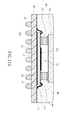
FIG. 4 , an image sensor packaging structure with a predetermined focal length according to a second embodiment of the present invention further includes afirst lens 70 and asecond lens 71. Thefirst lens 70 and thesecond lens 71 are coupled to thefifth surface 331 and thesixth surface 332 of the first light-transparent lid 33, respectively. At least one of thefirst lens 70 and thesecond lens 71 is an aspherical lens, and each of thefirst lens 70 and thesecond lens 71 can be a spherical lens or an aspherical lens. Moreover, aninfrared filter layer 80 is provided between thesecond lens 71 and thesixth surface 332 of the first light-transparent lid 33, and a first light-shielding layer 90 can be further provided on theinfrared filter layer 80. The first light-shielding layer 90 is formed with afirst window 100 corresponding in position to thesecond lens 71. - Alternatively, the
infrared filter layer 80 is provided between thefirst lens 70 and thefifth surface 331 of the first light-transparent lid 33 (not shown), rather than between thesecond lens 71 and thesixth surface 332 of the first light-transparent lid 33. However, regardless of where theinfrared filter layer 80 is located, there can only be one single-sidedinfrared filter layer 80. While theinfrared filter layer 80 is provided between thefirst lens 70 and thefifth surface 331, the first light-shielding layer 90 can be provided on theinfrared filter layer 80. In this case, thefirst window 100 of the first light-shielding layer 90 corresponds in position to thefirst lens 70. As shown inFIG. 4 , the second embodiment further includes a plurality ofsolder pads 140 provided around the perimeter of thebottom surface 12 of thesubstrate 10 or arranged in an array (not shown). Thesolder pads 140 are electrically connected to the firstconductive contacts 111 via the circuit structure in thesubstrate 10. - Referring to
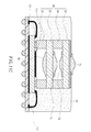
FIG. 5 andFIG. 6 , in a third embodiment, theoptical assembly 30 includes a second supportingframe 34, a second light-transparent lid 35, athird lens 72, and afourth lens 73, in addition to the first supportingframe 32, the first light-transparent lid 33, thefirst lens 70, and thesecond lens 71. The second supportingframe 34 has aseventh surface 341 and aneighth surface 342, wherein theseventh surface 341 is coupled to thesixth surface 332 of the first light-transparent lid 33. Furthermore, the second supportingframe 34 defines therein asecond opening 343 that corresponds in position to thefirst opening 323 of the first supportingframe 32. Thefirst lens 70, thesecond lens 71, thethird lens 72, and thefourth lens 73 can be either spherical or aspherical lenses, but at least one of them must be an aspherical lens. - The second light-
transparent lid 35 has aninth surface 351 and atenth surface 352, wherein theninth surface 351 is coupled to theeighth surface 342 of the second supportingframe 34. Besides, thethird lens 72 is coupled to theninth surface 351 of the second light-transparent lid 35 while thefourth lens 73 is coupled to thetenth surface 352 of the second light-transparent lid 35. Moreover, aninfrared filter layer 80 is provided between thefourth lens 73 and thetenth surface 352, and a second light-shielding layer 91 can be further provided on theinfrared filter layer 80, wherein the second light-shielding layer 91 is formed with asecond window 101 that corresponds in position to thefourth lens 73. - The
dam 40 is formed around the perimeter of thetenth surface 352. While theinfrared filter layer 80 and /or the second light-shielding layer 91 is provided on thetenth surface 352, thedam 40 can be formed on the infrared filter layer 80 (not shown) or the second light-shielding layer 91 (as shown inFIG. 5 andFIG. 6 ). Alternatively, like the second embodiment, the third embodiment may be configured in such a way that theinfrared filter layer 80 is provided between thethird lens 72 and theninth surface 351 while the second light-shielding layer 91 is provided on theinfrared filter layer 80. Moreover, thesecond window 101 of the second light-shielding layer 91 corresponds in position to thethird lens 72. In another alternative, the second light-shielding layer 91 is provided around the perimeter of thetenth surface 352, wherein thesecond window 101 of the second light-shielding layer 91 corresponds in position to thefourth lens 73. - In a fourth embodiment of the present invention as shown in
FIG. 7 andFIG. 8 , theoptical assembly 30 includes alens barrel 150, at least one third light-transparent lid 36, and at least twofifth lenses 74. Thelens barrel 150 has abottom surface 151 and atop surface 152, wherein thebottom surface 151 is coupled to thesecond surface 22 of thechip 20 between thesensitization area 221 and the secondconductive contacts 23. In addition, thedam 40 is formed around a perimeter of thetop surface 152 of thelens barrel 150. - The third light-
transparent lids 36 are fixedly provided in thelens barrel 150. Each third light-transparent lid 36 has aneleventh surface 361 and atwelfth surface 362. Thefifth lenses 74 are coupled to theeleventh surfaces 361 and thetwelfth surfaces 362, respectively. Aninfrared filter layer 80 is provided between one of thefifth lenses 74 and the correspondingtwelfth surface 362. Alternatively, as in the previous embodiments, theinfrared filter layer 80 is provided between one of thefifth lenses 74 and the corresponding eleventh surface 361 (not shown), rather than between one of thefifth lenses 74 and the correspondingtwelfth surface 362. However, no matter where theinfrared filter layer 80 is located, there can only be one single-sidedinfrared filter layer 80. - Referring to
FIG. 9 andFIG. 10 , in a fifth embodiment, theoptical assembly 30 includes a fourth light-transparent lid 37, a third supportingframe 38, a fifth light-transparent lid 39, asixth lens 75, and aseventh lens 76. The fourth light-transparent lid 37 has athirteenth surface 371 and afourteenth surface 372. The fourth light-transparent lid 37 is peripherally coupled to thesecond surface 22 of thechip 20 via thethirteenth surface 371 and anadhesive layer 120, wherein theadhesive layer 120 is located between thesensitization area 221 and the secondconductive contacts 23. Further, aninfrared filter layer 80 is provided on thethirteenth surface 371. - The third supporting
frame 38 has afifteenth surface 381 and asixteenth surface 382, wherein thefifteenth surface 381 is coupled to thefourteenth surface 372. Also, the third supportingframe 38 defines therein athird opening 383 that corresponds in position to thesensitization area 221 of thechip 20. Moreover, thedam 40 is formed around a perimeter of thesixteenth surface 382. The fifth light-transparent lid 39, which has aseventeenth surface 391 and aneighteenth surface 392, is fixedly provided in thethird opening 383 and fixed to the third supportingframe 38. As shown inFIG. 9 andFIG. 10 , thesixth lens 75 is coupled to theseventeenth surface 391 while theseventh lens 76 is coupled to theeighteenth surface 392. Furthermore, a third light-shielding layer 92 is provided on theeighteenth surface 392 and formed with athird window 102 that corresponds in position to theseventh lens 76. - It can be known from the description of the foregoing embodiments that the
optical assembly 30 is assembled and tested in advance and therefore does not require a focus adjusting procedure. In consequence, the manufacturing process is simplified, and the costs of equipment, man power, and materials are substantially reduced. Apart from that, theencapsulation compound 50 can be formed by transfer molding regardless of the configuration of the image sensor packaging structure, thus significantly shortening the cycle time of the manufacturing process and increasing the throughput per time unit while lowering related costs indirectly. - Additionally, as the
encapsulation compound 50 is formed with a mold during transfer molding, it is necessary to subject the mold to a certain pressure. Thedam 40, which is provided between the mold and theoptical assembly 30 and stays adequately resilient, not only functions as a buffer between the mold and theoptical assembly 30 to prevent theoptical assembly 30 from damage, but also conveys the pressure to the assembled and testedoptical assembly 30, thus providing a leveling effect, by which the inclination of theoptical assembly 30 relative to thechip 20 is reduced. In consequence, the optical focal length of theoptical assembly 30 is then more readily positioned on the sensitization area 221of thechip 20. - Even more advantageously, the
dam 40 provided around the perimeter of the top surface of theoptical assembly 30 serves as a barrier wall between theoptical assembly 30 and the upper mold section. Due to thedam 40, theencapsulation compound 50 is blocked outside theoptical assembly 30 and keeps theencapsulation compound 50 from overflowing to theoptical assembly 30. Further, as the upper mold section is in direct and close contact with thedam 40, the upper mold section does not make direct contact with theoptical assembly 30 and is therefore prevented from damaging or causing surface contamination to theoptical assembly 30. - In addition to being formed by molding process, the
encapsulation compound 50 may also be formed on thesubstrate 10 by a dispensing process. When the dispensing process is adopted, it is no longer necessary to provide the at least onedam 40 on theoptical assembly 30, and yet theoptical assembly 30 may still take on the various aspects described above. As shown inFIGS. 11A through 11D , the encapsulation compounds 50 are formed on theirrespective substrates 10 by a dispensing process without anydam 40 on theoptical assemblies 30. Consequently, the overall heights of the image sensor packaging structures are reduced to effectively downsize the image sensor packaging structures. - The foregoing embodiments are illustrative of the characteristics of the present invention so as to enable a person skilled in the art to understand the contents disclosed herein and implement the present invention accordingly. The embodiments, however, are not intended to restrict the scope of the present invention, which is defined only by the appended claims. Hence, all equivalent modifications and changes which do no depart from the spirit of the present invention should be encompassed by the claims.
Claims (22)
- An image sensor packaging structure with a predetermined focal length, comprising:a substrate (10) having a supporting surface (11) and a bottom surface (12), the
supporting surface (11) being formed with a plurality of first conductive contacts (111);a chip (20) having a first surface (21) coupled to the supporting surface (11) of the
substrate (10) and a second surface (22) having a sensitization area (221), the chip (20) further comprising a plurality of second conductive contacts (23) which are arranged around the sensitization area (221) and are electrically connected to the first conductive contacts (111) of the substrate (10);an optical assembly (30) coupled to the second surface (22) of the chip (20) and
disposed above the sensitization area (221) of the chip (20) so as to cover the sensitization area (221) and thus form an air cavity (31), the optical assembly (30) having a predetermined focal length; andan encapsulation compound (50) formed to surround the chip (20) and the optical
assembly (30). - The image sensor packaging structure of claim 1, wherein the chip (20) is a complementary metal oxide semiconductor (CMOS) image sensor chip or a charge-coupled device (CCD).
- The image sensor packaging structure of claim 1, wherein the sensitization area (221) is composed of a plurality of photosensitive elements.
- The image sensor packaging structure of claim 1, further comprising at least one dam (40) provided around a perimeter of a top surface of the optical assembly (30), wherein the encapsulation compound (50) is formed on the substrate (10) by molding process, so as to surround the chip (20), the optical assembly (30), and the at least one dam (40).
- The image sensor packaging structure of claim 4, wherein the optical assembly (30) comprises:a first supporting frame (32) having a third surface (321) and a fourth surface (322),
the third surface (321) being coupled to the second surface (22) of the chip (20) between the sensitization area (221) and the second conductive contacts (23) of the chip (20), the first supporting frame (32) defining therein a first opening (323) corresponding in position to the sensitization area (221); anda first light-transparent lid (33) having a fifth surface (331) and a sixth surface (332),
the fifth surface (331) being coupled to the fourth surface (322), wherein the at least one dam (40) is provided around a perimeter of the sixth surface (332). - The image sensor packaging structure of claim 5, further comprising: a first lens (70) coupled to the fifth surface (331) of the first light-transparent lid (33); and a second lens (71) coupled to the sixth surface (332) of the first light-transparent lid (33).
- The image sensor packaging structure of claim 6, wherein at least one of the first lens (70) and the second lens (71) is an aspherical lens.
- The image sensor packaging structure of claim 6, wherein the first lens (70) is a spherical lens or an aspherical lens.
- The image sensor packaging structure of claim 6, wherein the second lens (71) is a spherical lens or an aspherical lens.
- The image sensor packaging structure of claim 4, wherein the optical assembly (30) comprises:a first supporting frame (32) having a third surface (321) and a fourth surface (322),
the third surface (321) being coupled to the second surface (22) of the chip (20) between the sensitization area (221) and the second conductive contacts (23), the first supporting frame (32) defining therein a first opening (323) corresponding in position to the sensitization area (221);a first light-transparent lid (33) having a fifth surface (331) and a sixth surface (332),
the fifth surface (331) being coupled to the fourth surface (322);a first lens (70) coupled to the fifth surface (331);a second lens (71) coupled to the sixth surface (332);a second supporting frame (34) having a seventh surface (341) and an eighth surface (342), the seventh surface (341) being coupled to the sixth surface (332), the second supporting frame (34) defining therein a second opening (343) corresponding in position to the first opening (323);a second light-transparent lid (35) having a ninth surface (351) and a tenth surface (352), the ninth surface (351) being coupled to the eighth surface (342);a third lens (72) coupled to the ninth surface (351); anda fourth lens (73) coupled to the tenth surface (352), wherein the at least one dam (40)
is provided around a perimeter of the tenth surface (352). - The image sensor packaging structure of claim 4, wherein the optical assembly (30) comprises:a lens barrel (150) having a bottom surface (151) and a top surface (152), the bottom
surface (151) being coupled to the second surface (22) of the chip (20) between the sensitization area (221) and the second conductive contacts (23), wherein the at least one dam (40) is provided around a perimeter of the top surface (152);at least one third light-transparent lid (36) fixedly provided in the lens barrel (150),
each said third light-transparent lid (36) having an eleventh surface (361) and a twelfth surface (362); andat least two fifth lenses (74) coupled to the eleventh surface (361) and the twelfth
surface (362) of a said third light-transparent lid (36), respectively. - The image sensor packaging structure of claim 4, wherein the optical assembly (30) comprises:a fourth light-transparent lid (37) having a thirteenth surface (371) and a fourteenth
surface (372), the fourth light-transparent lid (37) being peripherally coupled to the second surface (22) of the chip (20) via the thirteenth surface (371) and an adhesive layer (120), the adhesive layer (120) being provided between the sensitization area (221) and the second conductive contacts (23);a third supporting frame (38) having a fifteenth surface (381) and a sixteenth surface (382), the fifteenth surface (381) being coupled to the fourteenth surface (372), the third supporting frame (38) defining therein a third opening (383) corresponding in position to the sensitization area (221), wherein the at least one dam (40) is provided around a perimeter of the sixteenth surface (382);a fifth light-transparent lid (39) fixedly provided in the third opening (383), fixed to
the third supporting frame (38), and having a seventeenth surface (391) and an eighteenth surface (392);a sixth lens (75) coupled to the seventeenth surface (391); anda seventh lens (76) coupled to the eighteenth surface (392). - The image sensor packaging structure of claim 4, wherein the at least one dam (40) is made of epoxy or a film.
- The image sensor packaging structure of claim 1, wherein the encapsulation compound (50) is formed on the substrate (10) by dispensing, so as to surround the chip (20) and the optical assembly (30).
- The image sensor packaging structure of claim 1, wherein the optical assembly (30) comprises:a first supporting frame (32) having a third surface (321) and a fourth surface (322),
the third surface (321) being coupled to the second surface (22) of the chip (20) between the sensitization area (221) and the second conductive contacts (23) of the chip (20), the first supporting frame (32) defining therein a first opening (323) corresponding in position to the sensitization area (221); anda first light-transparent lid (33) having a fifth surface (331) and a sixth surface (332),
the fifth surface (331) being coupled to the fourth surface (322). - The image sensor packaging structure of claim 15, further comprising: a first lens (70) coupled to the fifth surface (331) of the first light-transparent lid (33); and a second lens (71) coupled to the sixth surface (332) of the first light-transparent lid (33).
- The image sensor packaging structure of claim 16, wherein at least one of the first lens (70) and the second lens (71) is an aspherical lens.
- The image sensor packaging structure of claim 16, wherein the first lens (70) is a spherical lens or an aspherical lens.
- The image sensor packaging structure of claim 16, wherein the second lens (71) is a spherical lens or an aspherical lens.
- The image sensor packaging structure of claim 1, wherein the optical assembly (30) comprises:a first supporting frame (32) having a third surface (321) and a fourth surface (322),
the third surface (321) being coupled to the second surface (22) of the chip (20) between the sensitization area (221) and the second conductive contacts (23), the first supporting frame (32) defining therein a first opening (323) corresponding in position to the sensitization area (221);a first light-transparent lid (33) having a fifth surface (331) and a sixth surface (332),
the fifth surface (331) being coupled to the fourth surface (322);a first lens (70) coupled to the fifth surface (331);a second lens (71) coupled to the sixth surface (332);a second supporting frame (34) having a seventh surface (341) and an eighth surface (342), the seventh surface (341) being coupled to the sixth surface (332), the second supporting frame (34) defining therein a second opening (343) corresponding in position to the first opening (323);a second light-transparent lid (35) having a ninth surface (351) and a tenth surface (352), the ninth surface (351) being coupled to the eighth surface (342);a third lens (72) coupled to the ninth surface (351); anda fourth lens (73) coupled to the tenth surface (352). - The image sensor packaging structure of claim 1, wherein the optical assembly (30) comprises:a lens barrel (150) having a bottom surface (151) and a top surface (152), the bottom
surface (151) being coupled to the second surface (22) of the chip (20) between the sensitization area (221) and the second conductive contacts (23);at least one third light-transparent lid (36) fixedly provided in the lens barrel (150),
each said third light-transparent lid (36) having an eleventh surface (361) and a twelfth surface (362); andat least two fifth lenses (74) coupled to the eleventh surface (361) and the twelfth
surface (362) of a said third light-transparent lid (36), respectively. - The image sensor packaging structure of claim 1, wherein the optical assembly (30) comprises:a fourth light-transparent lid (37) having a thirteenth surface (371) and a fourteenth
surface (372), the fourth light-transparent lid (37) peripherally coupled to the second surface (22) of the chip (20) via the thirteenth surface (371) and an adhesive layer (120), the adhesive layer (120) being provided between the sensitization area (221) and the second conductive contacts (23);a third supporting frame (38) having a fifteenth surface (381) and a sixteenth surface (382), the fifteenth surface (381) being coupled to the fourteenth surface (372), the third supporting frame (38) defining therein a third opening (383) corresponding in position to the sensitization area (221);a fifth light-transparent lid (39) fixedly provided in the third opening (383), fixed to
the third supporting frame (38), and having a seventeenth surface (391) and an eighteenth surface (392);a sixth lens (75) coupled to the seventeenth surface (391); anda seventh lens (76) coupled to the eighteenth surface (392).
Applications Claiming Priority (1)
| Application Number | Priority Date | Filing Date | Title |
|---|---|---|---|
| TW098146153A TWI425825B (en) | 2009-12-31 | 2009-12-31 | Image sensor package structure with predetermined focus |
Publications (2)
| Publication Number | Publication Date |
|---|---|
| EP2341541A2 true EP2341541A2 (en) | 2011-07-06 |
| EP2341541A3 EP2341541A3 (en) | 2012-08-08 |
Family
ID=43416310
Family Applications (1)
| Application Number | Title | Priority Date | Filing Date |
|---|---|---|---|
| EP10187111A Withdrawn EP2341541A3 (en) | 2009-12-31 | 2010-10-11 | Image sensor packaging structure with predetermined focal length |
Country Status (3)
| Country | Link |
|---|---|
| US (1) | US8441086B2 (en) |
| EP (1) | EP2341541A3 (en) |
| TW (1) | TWI425825B (en) |
Cited By (5)
| Publication number | Priority date | Publication date | Assignee | Title |
|---|---|---|---|---|
| EP2432017A3 (en) * | 2010-09-17 | 2013-02-27 | Kingpak Technology Inc. | Manufacturing method of molded image sensor packaging structure with predetermined focal length and the structure using the same |
| CN108401094A (en) * | 2017-02-08 | 2018-08-14 | 宁波舜宇光电信息有限公司 | Array camera module and its molding photosensory assembly and manufacturing method and the electronic equipment with array camera module |
| CN108649041A (en) * | 2018-04-16 | 2018-10-12 | 复旦大学 | A kind of chip-packaging structure and its method based on composite interconnection substrate |
| CN110278426A (en) * | 2018-03-18 | 2019-09-24 | 宁波舜宇光电信息有限公司 | Depth information camera module and its base assembly, electronic equipment and preparation method |
| WO2020094101A1 (en) * | 2018-11-09 | 2020-05-14 | 昆山丘钛微电子科技有限公司 | Camera module and manufacturing method therefor, and terminal |
Families Citing this family (22)
| Publication number | Priority date | Publication date | Assignee | Title |
|---|---|---|---|---|
| JP2013118230A (en) * | 2011-12-01 | 2013-06-13 | Canon Inc | Solid-state imaging device |
| JP6096812B2 (en) | 2013-01-22 | 2017-03-15 | 京セラ株式会社 | Electronic device mounting package, electronic device and imaging module |
| WO2014119729A1 (en) * | 2013-01-31 | 2014-08-07 | 京セラ株式会社 | Substrate for mounting electronic element, electronic device, and imaging module |
| US10211191B2 (en) * | 2014-08-06 | 2019-02-19 | Pixart Imaging Inc. | Image module package with transparent sub-assembly |
| CN107924809B (en) | 2015-07-09 | 2022-09-13 | 赫普塔冈微光有限公司 | Optoelectronic module including a package supporting an optical assembly |
| KR102195988B1 (en) * | 2016-02-18 | 2020-12-29 | 닝보 써니 오포테크 코., 엘티디. | Array imaging module and molded photosensitive assembly, cirduit board assembly and manufacturing method thereof for electronic device |
| US10908324B2 (en) * | 2016-03-12 | 2021-02-02 | Ningbo Sunny Opotech Co., Ltd. | Molded photosensitive assembly of array imaging module |
| CN111193852B (en) * | 2016-03-28 | 2021-10-15 | 宁波舜宇光电信息有限公司 | Camera module and manufacturing method thereof |
| US9798054B1 (en) * | 2016-03-30 | 2017-10-24 | Delphi Technologies, Inc. | Camera assembly for use on a vehicle |
| US10925160B1 (en) | 2016-06-28 | 2021-02-16 | Amazon Technologies, Inc. | Electronic device with a display assembly and silicon circuit board substrate |
| TWI635348B (en) * | 2017-05-12 | 2018-09-11 | 海華科技股份有限公司 | Portable electronic device and image-capturing module thereof, and carrier assembly thereof |
| CN109427829B (en) * | 2017-09-01 | 2020-09-15 | 胜丽国际股份有限公司 | Sensor package structure |
| CN109672806B (en) * | 2017-10-13 | 2022-06-28 | 宁波舜宇光电信息有限公司 | Camera module, photosensitive assembly and packaging method thereof |
| CN107770422A (en) * | 2017-10-25 | 2018-03-06 | 信利光电股份有限公司 | The preparation method and electronic equipment of a kind of camera module |
| CN110649047A (en) * | 2018-06-26 | 2020-01-03 | 三赢科技(深圳)有限公司 | Photosensitive chip packaging structure and forming method thereof |
| WO2020192439A1 (en) * | 2019-03-22 | 2020-10-01 | 宁波舜宇光电信息有限公司 | Camera module, lens assembly and manufacturing method thereof, and electronic device comprising camera module |
| US11444111B2 (en) * | 2019-03-28 | 2022-09-13 | Semiconductor Components Industries, Llc | Image sensor package having a light blocking member |
| TWI689018B (en) * | 2019-04-23 | 2020-03-21 | 鴻海精密工業股份有限公司 | Image sensor package atructure, lens module and electronic device |
| CN115004679A (en) * | 2020-03-17 | 2022-09-02 | 索尼半导体解决方案公司 | Sensor package, method of manufacturing the same, and imaging device |
| CN112201667A (en) * | 2020-11-06 | 2021-01-08 | 积高电子(无锡)有限公司 | POP packaging structure and packaging method of image sensor |
| GB202102011D0 (en) * | 2021-02-12 | 2021-03-31 | Ams Sensors Singapore Pte Ltd | Optoelectronic module |
| WO2024022217A1 (en) * | 2022-07-27 | 2024-02-01 | 宁波舜宇光电信息有限公司 | Camera module and manufacturing method therefor |
Citations (1)
| Publication number | Priority date | Publication date | Assignee | Title |
|---|---|---|---|---|
| US6972497B2 (en) | 2002-02-06 | 2005-12-06 | Stmicroelectronics S.A. | Optical semiconductor device and method of manufacture |
Family Cites Families (20)
| Publication number | Priority date | Publication date | Assignee | Title |
|---|---|---|---|---|
| AU2001253547A1 (en) * | 2000-05-23 | 2001-12-03 | Atmel Corporation | Integrated ic chip package for electronic image sensor die |
| JP2005072978A (en) * | 2003-08-25 | 2005-03-17 | Renesas Technology Corp | Solid state imaging device and its manufacturing method |
| KR100539234B1 (en) * | 2003-06-11 | 2005-12-27 | 삼성전자주식회사 | A CMOS type image sensor module having transparent polymeric encapsulation material |
| US6849915B1 (en) * | 2003-08-26 | 2005-02-01 | Ultra Tera Corporation | Light sensitive semiconductor package and fabrication method thereof |
| DE10344760A1 (en) * | 2003-09-26 | 2005-05-04 | Siemens Ag | Optical module and optical system |
| JP2006148710A (en) * | 2004-11-22 | 2006-06-08 | Sharp Corp | Imaging module and method of manufacturing the same |
| TW200714043A (en) * | 2005-09-05 | 2007-04-01 | Altus Technology Inc | Image sensor package and digital camera module therewith |
| JP4382030B2 (en) * | 2005-11-15 | 2009-12-09 | 富士通マイクロエレクトロニクス株式会社 | Semiconductor device and manufacturing method thereof |
| US20080203512A1 (en) * | 2006-06-07 | 2008-08-28 | Hon Hai Precision Industry Co., Ltd. | Image sensor chip package |
| JPWO2008132980A1 (en) * | 2007-04-17 | 2010-07-22 | コニカミノルタオプト株式会社 | Imaging device manufacturing method, imaging device, and portable terminal |
| TWI351217B (en) * | 2007-04-27 | 2011-10-21 | Hon Hai Prec Ind Co Ltd | Imageing module |
| JP4384202B2 (en) * | 2007-05-31 | 2009-12-16 | シャープ株式会社 | Semiconductor device and optical device module including the same |
| JP4378394B2 (en) * | 2007-05-31 | 2009-12-02 | シャープ株式会社 | Semiconductor device and optical device module including the same |
| TWI346221B (en) * | 2007-06-15 | 2011-08-01 | Hon Hai Prec Ind Co Ltd | Camera module and image sensor package structure |
| US7923298B2 (en) * | 2007-09-07 | 2011-04-12 | Micron Technology, Inc. | Imager die package and methods of packaging an imager die on a temporary carrier |
| US20110031510A1 (en) * | 2007-11-27 | 2011-02-10 | Heptagon Oy | Encapsulated lens stack |
| US20090206431A1 (en) * | 2008-02-20 | 2009-08-20 | Micron Technology, Inc. | Imager wafer level module and method of fabrication and use |
| US8004602B2 (en) * | 2008-05-16 | 2011-08-23 | Kingpak Technology Inc. | Image sensor structure and integrated lens module thereof |
| CN101924081A (en) * | 2009-06-15 | 2010-12-22 | 鸿富锦精密工业(深圳)有限公司 | Image sensor package and image sensor module |
| TW201104850A (en) * | 2009-07-29 | 2011-02-01 | Kingpak Tech Inc | Image sensor package structure with large air cavity |
-
2009
- 2009-12-31 TW TW098146153A patent/TWI425825B/en not_active IP Right Cessation
-
2010
- 2010-10-11 EP EP10187111A patent/EP2341541A3/en not_active Withdrawn
- 2010-11-16 US US12/947,210 patent/US8441086B2/en not_active Expired - Fee Related
Patent Citations (1)
| Publication number | Priority date | Publication date | Assignee | Title |
|---|---|---|---|---|
| US6972497B2 (en) | 2002-02-06 | 2005-12-06 | Stmicroelectronics S.A. | Optical semiconductor device and method of manufacture |
Cited By (10)
| Publication number | Priority date | Publication date | Assignee | Title |
|---|---|---|---|---|
| EP2432017A3 (en) * | 2010-09-17 | 2013-02-27 | Kingpak Technology Inc. | Manufacturing method of molded image sensor packaging structure with predetermined focal length and the structure using the same |
| US8481343B2 (en) | 2010-09-17 | 2013-07-09 | Kingpak Technology Inc. | Manufacturing method of molded image sensor packaging structure with predetermined focal length and the structure using the same |
| CN108401094A (en) * | 2017-02-08 | 2018-08-14 | 宁波舜宇光电信息有限公司 | Array camera module and its molding photosensory assembly and manufacturing method and the electronic equipment with array camera module |
| EP3582484A4 (en) * | 2017-02-08 | 2020-11-04 | Ningbo Sunny Opotech Co., Ltd. | Camera module, moulded photosensitive component thereof, manufacturing method therefor, and electronic device |
| US10979610B2 (en) | 2017-02-08 | 2021-04-13 | Ningbo Sunny Opotech Co., Ltd. | Camera module, molding photosensitive assembly thereof, manufacturing method and electronic device |
| CN110278426A (en) * | 2018-03-18 | 2019-09-24 | 宁波舜宇光电信息有限公司 | Depth information camera module and its base assembly, electronic equipment and preparation method |
| CN110278426B (en) * | 2018-03-18 | 2024-02-13 | 宁波舜宇光电信息有限公司 | Depth information camera module, base assembly thereof, electronic equipment and preparation method |
| CN108649041A (en) * | 2018-04-16 | 2018-10-12 | 复旦大学 | A kind of chip-packaging structure and its method based on composite interconnection substrate |
| CN108649041B (en) * | 2018-04-16 | 2021-01-26 | 复旦大学 | Chip packaging structure based on composite interconnection substrate and method thereof |
| WO2020094101A1 (en) * | 2018-11-09 | 2020-05-14 | 昆山丘钛微电子科技有限公司 | Camera module and manufacturing method therefor, and terminal |
Also Published As
| Publication number | Publication date |
|---|---|
| TW201123858A (en) | 2011-07-01 |
| EP2341541A3 (en) | 2012-08-08 |
| TWI425825B (en) | 2014-02-01 |
| US20110156187A1 (en) | 2011-06-30 |
| US8441086B2 (en) | 2013-05-14 |
Similar Documents
| Publication | Publication Date | Title |
|---|---|---|
| US8441086B2 (en) | Image sensor packaging structure with predetermined focal length | |
| EP2393116B1 (en) | Wafer level image sensor packaging structure and manufacturing method for the same | |
| US8928104B2 (en) | Image sensor packaging structure with black encapsulant | |
| US11824071B2 (en) | Camera module and molded photosensitive assembly and manufacturing method thereof, and electronic device | |
| US20220021792A1 (en) | Array camera module and application thereof | |
| US7576401B1 (en) | Direct glass attached on die optical module | |
| CN111193852B (en) | Camera module and manufacturing method thereof | |
| JP4673721B2 (en) | Imaging apparatus and manufacturing method thereof | |
| KR101070058B1 (en) | Camera Module Package | |
| CN107566691B (en) | Photosensitive assembly, camera module and manufacturing method thereof | |
| EP2432017B1 (en) | Manufacturing method of molded image sensor packaging structure with predetermined focal length and the structure using the same | |
| US7863062B2 (en) | Semiconductor device with a shielding section to prevent condensation and optical device module having the semiconductor device | |
| US20070287216A1 (en) | Microelectronic imaging units and methods of manufacturing microelectronic imaging units | |
| US8110884B2 (en) | Methods of packaging imager devices and optics modules, and resulting assemblies | |
| US20090256222A1 (en) | Packaging method of image sensing device | |
| CN108401091B (en) | Camera module and molded circuit board assembly and application thereof | |
| EP3484139B1 (en) | Photosensitive component, and camera module | |
| EP3562136A2 (en) | Image-capturing module, circuit board assembly, manufacturing method, and electronic device provided with image-capturing module | |
| US8952412B2 (en) | Method for fabricating a solid-state imaging package | |
| US20090215216A1 (en) | Packaging method of image sensing device | |
| CN107734215B (en) | Image pickup module, molded photosensitive assembly thereof, manufacturing method of molded photosensitive assembly and electronic equipment | |
| EP3754726A1 (en) | Integrated photosensitive module, photosensitive assembly, camera module and preparation method therefor | |
| CN109672806B (en) | Camera module, photosensitive assembly and packaging method thereof | |
| US20210185195A1 (en) | Imaging unit and imaging device | |
| CN111277734B (en) | Image pickup module and manufacturing method thereof |
Legal Events
| Date | Code | Title | Description |
|---|---|---|---|
| PUAI | Public reference made under article 153(3) epc to a published international application that has entered the european phase |
Free format text: ORIGINAL CODE: 0009012 |
|
| AK | Designated contracting states |
Kind code of ref document: A2 Designated state(s): AL AT BE BG CH CY CZ DE DK EE ES FI FR GB GR HR HU IE IS IT LI LT LU LV MC MK MT NL NO PL PT RO RS SE SI SK SM TR |
|
| AX | Request for extension of the european patent |
Extension state: BA ME |
|
| RIC1 | Information provided on ipc code assigned before grant |
Ipc: H01L 27/146 20060101AFI20120322BHEP |
|
| PUAL | Search report despatched |
Free format text: ORIGINAL CODE: 0009013 |
|
| AK | Designated contracting states |
Kind code of ref document: A3 Designated state(s): AL AT BE BG CH CY CZ DE DK EE ES FI FR GB GR HR HU IE IS IT LI LT LU LV MC MK MT NL NO PL PT RO RS SE SI SK SM TR |
|
| AX | Request for extension of the european patent |
Extension state: BA ME |
|
| RIC1 | Information provided on ipc code assigned before grant |
Ipc: H01L 27/146 20060101AFI20120704BHEP |
|
| 17P | Request for examination filed |
Effective date: 20130118 |
|
| 17Q | First examination report despatched |
Effective date: 20130219 |
|
| RAP1 | Party data changed (applicant data changed or rights of an application transferred) |
Owner name: KINGPAK TECHNOLOGY INC. |
|
| STAA | Information on the status of an ep patent application or granted ep patent |
Free format text: STATUS: THE APPLICATION IS DEEMED TO BE WITHDRAWN |
|
| 18D | Application deemed to be withdrawn |
Effective date: 20160503 |