EP2330172B1 - Method for manufacturing phosphor and light emitting device comprising the phosphor - Google Patents
Method for manufacturing phosphor and light emitting device comprising the phosphor Download PDFInfo
- Publication number
- EP2330172B1 EP2330172B1 EP10193699.5A EP10193699A EP2330172B1 EP 2330172 B1 EP2330172 B1 EP 2330172B1 EP 10193699 A EP10193699 A EP 10193699A EP 2330172 B1 EP2330172 B1 EP 2330172B1
- Authority
- EP
- European Patent Office
- Prior art keywords
- fluorescent material
- solution
- nano
- light emitting
- silicate based
- Prior art date
- Legal status (The legal status is an assumption and is not a legal conclusion. Google has not performed a legal analysis and makes no representation as to the accuracy of the status listed.)
- Not-in-force
Links
Images

Classifications
-
- C—CHEMISTRY; METALLURGY
- C09—DYES; PAINTS; POLISHES; NATURAL RESINS; ADHESIVES; COMPOSITIONS NOT OTHERWISE PROVIDED FOR; APPLICATIONS OF MATERIALS NOT OTHERWISE PROVIDED FOR
- C09K—MATERIALS FOR MISCELLANEOUS APPLICATIONS, NOT PROVIDED FOR ELSEWHERE
- C09K11/00—Luminescent, e.g. electroluminescent, chemiluminescent materials
- C09K11/02—Use of particular materials as binders, particle coatings or suspension media therefor
-
- C—CHEMISTRY; METALLURGY
- C09—DYES; PAINTS; POLISHES; NATURAL RESINS; ADHESIVES; COMPOSITIONS NOT OTHERWISE PROVIDED FOR; APPLICATIONS OF MATERIALS NOT OTHERWISE PROVIDED FOR
- C09K—MATERIALS FOR MISCELLANEOUS APPLICATIONS, NOT PROVIDED FOR ELSEWHERE
- C09K11/00—Luminescent, e.g. electroluminescent, chemiluminescent materials
- C09K11/08—Luminescent, e.g. electroluminescent, chemiluminescent materials containing inorganic luminescent materials
- C09K11/77—Luminescent, e.g. electroluminescent, chemiluminescent materials containing inorganic luminescent materials containing rare earth metals
- C09K11/7728—Luminescent, e.g. electroluminescent, chemiluminescent materials containing inorganic luminescent materials containing rare earth metals containing europium
- C09K11/77342—Silicates
-
- H—ELECTRICITY
- H10—SEMICONDUCTOR DEVICES; ELECTRIC SOLID-STATE DEVICES NOT OTHERWISE PROVIDED FOR
- H10H—INORGANIC LIGHT-EMITTING SEMICONDUCTOR DEVICES HAVING POTENTIAL BARRIERS
- H10H20/00—Individual inorganic light-emitting semiconductor devices having potential barriers, e.g. light-emitting diodes [LED]
- H10H20/80—Constructional details
- H10H20/85—Packages
- H10H20/851—Wavelength conversion means
- H10H20/8511—Wavelength conversion means characterised by their material, e.g. binder
- H10H20/8512—Wavelength conversion materials
- H10H20/8513—Wavelength conversion materials having two or more wavelength conversion materials
-
- H—ELECTRICITY
- H01—ELECTRIC ELEMENTS
- H01L—SEMICONDUCTOR DEVICES NOT COVERED BY CLASS H10
- H01L2224/00—Indexing scheme for arrangements for connecting or disconnecting semiconductor or solid-state bodies and methods related thereto as covered by H01L24/00
- H01L2224/01—Means for bonding being attached to, or being formed on, the surface to be connected, e.g. chip-to-package, die-attach, "first-level" interconnects; Manufacturing methods related thereto
- H01L2224/42—Wire connectors; Manufacturing methods related thereto
- H01L2224/47—Structure, shape, material or disposition of the wire connectors after the connecting process
- H01L2224/48—Structure, shape, material or disposition of the wire connectors after the connecting process of an individual wire connector
- H01L2224/4805—Shape
- H01L2224/4809—Loop shape
- H01L2224/48091—Arched
-
- H—ELECTRICITY
- H01—ELECTRIC ELEMENTS
- H01L—SEMICONDUCTOR DEVICES NOT COVERED BY CLASS H10
- H01L2224/00—Indexing scheme for arrangements for connecting or disconnecting semiconductor or solid-state bodies and methods related thereto as covered by H01L24/00
- H01L2224/01—Means for bonding being attached to, or being formed on, the surface to be connected, e.g. chip-to-package, die-attach, "first-level" interconnects; Manufacturing methods related thereto
- H01L2224/42—Wire connectors; Manufacturing methods related thereto
- H01L2224/47—Structure, shape, material or disposition of the wire connectors after the connecting process
- H01L2224/48—Structure, shape, material or disposition of the wire connectors after the connecting process of an individual wire connector
- H01L2224/481—Disposition
- H01L2224/48151—Connecting between a semiconductor or solid-state body and an item not being a semiconductor or solid-state body, e.g. chip-to-substrate, chip-to-passive
- H01L2224/48221—Connecting between a semiconductor or solid-state body and an item not being a semiconductor or solid-state body, e.g. chip-to-substrate, chip-to-passive the body and the item being stacked
- H01L2224/48245—Connecting between a semiconductor or solid-state body and an item not being a semiconductor or solid-state body, e.g. chip-to-substrate, chip-to-passive the body and the item being stacked the item being metallic
- H01L2224/48247—Connecting between a semiconductor or solid-state body and an item not being a semiconductor or solid-state body, e.g. chip-to-substrate, chip-to-passive the body and the item being stacked the item being metallic connecting the wire to a bond pad of the item
-
- H—ELECTRICITY
- H10—SEMICONDUCTOR DEVICES; ELECTRIC SOLID-STATE DEVICES NOT OTHERWISE PROVIDED FOR
- H10H—INORGANIC LIGHT-EMITTING SEMICONDUCTOR DEVICES HAVING POTENTIAL BARRIERS
- H10H20/00—Individual inorganic light-emitting semiconductor devices having potential barriers, e.g. light-emitting diodes [LED]
- H10H20/01—Manufacture or treatment
- H10H20/036—Manufacture or treatment of packages
- H10H20/0361—Manufacture or treatment of packages of wavelength conversion means
Definitions
- the present invention relates to a method for manufacturing fluorescent body and a light emitting device including the fluorescent body manufactured by the manufacturing method.
- a light emitting diode (hereinafter, referred to as LED) can be used to configure a light emitting source by using a compound semiconductor material such as GaAs-based, AlGaAs-based, GaN-based, InGaN-based and InGaAlP-based material.
- EP 1 710 289 discloses a method of making a phosphor composition comprising the step of providing a first phosphor comprising a visible-light-emitting phosphor; providing a second phosphor having an average primary crystallite size of less than 100 nm; and disposing the second phosphor onto the first phosphor.
- WO 2008/122331 discloses a method of producing a phosphor material comprising the step of: suspending or dissolving at least two alkaline earth metals and a europium containing dopant in the form of salts, nitrates, oxalates, hydroxides or their mixtures in water, acids or bases; adding a silicon containing compound to the dispersion to form phosphor precursor at high temperature; adding an inorganic or an organic precipitating agent to this mixture; and converting the developed phosphor precursor by thermal after-treatment to the finished phosphor.
- One aspect of this invention is a method for manufacturing a fluorescent material.
- the method includes:
- the putting the fluorescent material into the first solution and agitating the fluorescent material and the first solution includes heating and agitating such that the temperature of the solution does not fall below a predetermined temperature.
- the light emitting device includes:
- Fig. 1 is a view showing a light emitting device of the present invention.
- a light emitting device 100 includes a package body 110, a light emitting element 120, a resin 125 and lead frames 132 and 134.
- the package body (110) is injected-molded in a predetermined shape by using at least one selected from the group consisting of PPA(Polyphthalamide), LCP(Liquid Crystal Polymer) and SPS(Syndiotactic polystyrene).
- a cavity 115 is formed having a constant depth in the upper part 112 of the package body 110.
- the circumference of the cavity 115 may be formed inclined at a predetermined angle with respect to an axis perpendicular to the bottom surface of the cavity 115.
- a plurality of the lead frames 132 and 134 are horizontally formed in the package body 110.
- the cavity having a shape of a reflective cup is formed on the upper part of the package body 110.
- the plurality of the lead frames 132 and 134 are exposed inside the cavity 115 and are electrically disconnected. Both ends of the plurality of the lead frames 132 and 134 are exposed to the outside of the package body 110 and are used as an electrode.
- a reflective material may be coated on the surfaces of the lead frames 132 and 134.
- the light emitting element 120 is die-bonded to a first lead frame 132 among the plurality of the lead frames 132 and 134.
- the light emitting element 120 is connected to the first lead frame 132 and a second lead frame 134 by means of a wire 122.
- the light emitting element 120 may correspond to at least one of colored light emitting diodes, for example, at least one selected from the group consisting of a red light emitting diode, a green light emitting diode, a blue light emitting diode and ultraviolet (UV) light emitting diode.
- a red light emitting diode for example, at least one selected from the group consisting of a red light emitting diode, a green light emitting diode, a blue light emitting diode and ultraviolet (UV) light emitting diode.
- UV ultraviolet
- the resin 125 is formed in the area of the cavity 115.
- the resin 125 includes a transparent silicon material or epoxy material.
- Fluorescent material 140 is added to the resin 125.
- the fluorescent material 140 may correspond to a silicate based fluorescent material. Particularly, nano-sized fluorescent materials are formed on a part of the surface of the fluorescent material 140.
- a convex lens may be formed on the resin 125.
- a protective device such as a zener diode for protecting the light emitting element 120 may be mounted on the plurality of the lead frames 132 and 134.
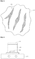
- the fluorescent material 140 added to the resin 125 may include many cracks 200 formed on the surface of the fluorescent material 140 (see Fig. 2 ).
- a plurality of the cracks having a shape depressed by a predetermined depth may be formed on the surface of the fluorescent material.
- the nano-sized fluorescent material is added to the fluorescent material in which the crack is formed such that the crack is filled with the nano-sized fluorescent material, i.e., nano-sized fluorescent powder (hereinafter, briefly referred to as a nano fluorescent material). That is, as shown in Fig. 3 , the cracks formed on the surface of the fluorescent material 140 are coated with or filled with sphere-shaped nano fluorescent material 300, so that it is possible to reduce the optical scattering caused by the cracks.
- the nano fluorescent material 300 may be formed by using a thermo spray decomposition method.
- the nano fluorescent material 300 having the same color and quality may be used as nano particles for smoothly filling the irregular structure of the fluorescent material 140.
- the nano fluorescent material 300 may include silicon based fluorescent material which is the same as fluorescer, for example, SrBaSiO:Eu.
- SrBaSiO:Eu silicon based fluorescent material which is the same as fluorescer
- the nano fluorescent material 300 and the fluorescent material 140 are attached to each other by van der vals force. As a result, luminous efficiency may be improved by as much as 20% to 30%.
- the sphere-shaped nano fluorescent material and a method of coating the nano fluorescent material on the surface (in particular, the crack) of the fluorescent material 140 will be described in detail.
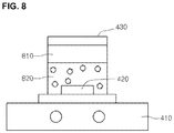
- Figs. 4 to 8 are views describing a method for manufacturing the fluorescent material in accordance with the embodiment of the present invention.
- agitator 410 and a beaker 430 being placed on the agitator and receiving solution. DI water solution 401 is put into the beaker 430 and a magnetic bar 420 is put into the beaker 430. Then, the agitator 410 is turned on.
- the magnetic bar 420 may not be fixed by a constituent such as an axis of rotation.
- the agitator 410 rotating the magnetic bar 420 does not contact with the magnetic bar 420 and is able to function as a magnetic agitator which rotates the magnetic bar 420 by applying a magnetic force from the outside.
- the magnetic agitator generates a rotating magnetic force by using a rotating electromagnet.
- a magnetic body (magnetic bar) external from the agitator is able to rotate by receiving the applied magnetic force.
- the agitator 410 is operated.
- the DI water 401 and the magnetic bar 420 are heated and agitated until the temperature of the DI water 401 reaches a predetermined temperature.
- the predetermined temperature is required to be about 50 degrees Celsius.
- ethanol, acetone, methanol and isopropyl alcohol and the like can be used instead of the DI water 401.
- more various solutions can be used according to embodiments.
- a fluorescent material 510 is put into the DI water 401 and is additionally agitated for about 30 minutes.
- the fluorescent material 510 may be composed of a silicate based material and have a mean particle diameter of 15 ⁇ m. However, since the size and kind of the fluorescent material can be variously changed according to a fluorescent material to be manufactured, more detailed description thereof will be omitted.
- the DI water 401 and the fluorescent material 510 are mixed in the beaker 430.
- a nano fluorescent material 610 is put into the beaker 430 and agitated.
- the nano fluorescent material 610 is composed of a fluorescent material having a size of from 100 nm to 400 nm. Through a thermo spray decomposition process, the nano fluorescent material having a nano size may be formed. If the size of the nano fluorescent material 610 is less than 100 nm, luminance may be deteriorated.
- the nano fluorescent material 610 is composed of a fluorescent material having the same color as that of the foregoing fluorescent material 510.
- the fluorescent material 510 is a yellow silicate fluorescent material
- the nano fluorescent material 610 is also formed of the yellow silicate fluorescent material. This intends that light having the same color is emitted through the resin to which the fluorescent material 510 is added, because the nano fluorescent material 610 is coated on the surface of the fluorescent material 510.
- 10gram of the nano fluorescent material 610 is put into the beaker 430.
- a predetermined amount of acetic acid is put into the beaker 430.
- 1Ml of the acetic acid together with the nano fluorescent material 610 are put into the beaker 430.
- the temperature of the solution in the beaker 430 should not be equal to or less than a predetermined temperature, preferably, about 50 degrees Celsius.
- the agitation is performed for about one hour.
- a person performing the embodiment checks the fluorescent material distribution, while checking the beaker 430.
- the reason why the acetic acid is put is that the nano fluorescent material 610 is well adsorbed into the cracks by etching the rough surface of the fluorescent material 510.
- Any solution capable of etching the surface of the fluorescent material 510, as well as the acetic acid can be variously used according to embodiments.
- a heater of the agitator 410 is turned off and the temperature of the solution of the beaker 430 is reduced.
- ZnSO 4 solution of 10% is put into the beaker 430 and more agitation is performed for about one hour.
- the reason why ZnSO 4 solution is put is that electrostatic force between particles of the solution is increased by ionizing the solution in the beaker 430, so that the nano fluorescent material 610 is better adsorbed on the surface of the fluorescent material 510.
- the agitator 410 is stopped and distribution state of the solution is checked. In other words, supernatant on the fluorescent material is checked whether it becomes transparent or not.
- the supernatant 810 is checked whether it becomes transparent or not and the agitation time may be increased or decreased according to the transparency of the supernatant 810. If the supernatant 810 becomes transparent (the transparency at this time can be variously determined according to embodiments or a person performing the embodiment), this means that the nano fluorescent material 610 is well adsorbed on the surface of the fluorescent material 510. Accordingly, the supernatant 810 is separated from a solution 820 including the fluorescent material. Here, it is possible to separate the supernatant 810 from the solution 820 including the fluorescent material by using a rotary pump. After the separation, the solution 820 including the fluorescent material is dried.
- the manufactured fluorescent material 510 corresponds to the fluorescent material 140 shown in Fig. 1 .
- Light emitted from the light emitting element 120 passes through a fluorescent material having a much reduced roughness of its surface, thereby reducing luminous efficiency degradation caused by light scatter.
Landscapes
- Chemical & Material Sciences (AREA)
- Engineering & Computer Science (AREA)
- Materials Engineering (AREA)
- Organic Chemistry (AREA)
- Inorganic Chemistry (AREA)
- Led Device Packages (AREA)
- Luminescent Compositions (AREA)
Applications Claiming Priority (1)
| Application Number | Priority Date | Filing Date | Title |
|---|---|---|---|
| KR1020090120181A KR101072162B1 (ko) | 2009-12-04 | 2009-12-04 | 형광체 제조방법 및 상기 형광체를 포함하는 발광장치 |
Publications (2)
| Publication Number | Publication Date |
|---|---|
| EP2330172A1 EP2330172A1 (en) | 2011-06-08 |
| EP2330172B1 true EP2330172B1 (en) | 2017-06-28 |
Family
ID=43587510
Family Applications (1)
| Application Number | Title | Priority Date | Filing Date |
|---|---|---|---|
| EP10193699.5A Not-in-force EP2330172B1 (en) | 2009-12-04 | 2010-12-03 | Method for manufacturing phosphor and light emitting device comprising the phosphor |
Country Status (6)
| Country | Link |
|---|---|
| US (1) | US8465798B2 (enExample) |
| EP (1) | EP2330172B1 (enExample) |
| JP (1) | JP5903212B2 (enExample) |
| KR (1) | KR101072162B1 (enExample) |
| CN (1) | CN102154002B (enExample) |
| TW (1) | TWI496871B (enExample) |
Families Citing this family (5)
| Publication number | Priority date | Publication date | Assignee | Title |
|---|---|---|---|---|
| KR101400343B1 (ko) * | 2012-02-10 | 2014-05-30 | 한국광기술원 | 상온 선택적 전극 보호 수용성 수지가 적용된 전극 노출형 침전 및 증발형 용제가 포함된 형광체 제조방법과 형광체 코팅층이 형성된 led 제조방법 |
| KR101945808B1 (ko) * | 2012-08-06 | 2019-02-08 | 엘지이노텍 주식회사 | 발광 소자 및 발광 소자 패키지 |
| TWI484664B (zh) * | 2012-09-11 | 2015-05-11 | Brightek Optoelectronic Co Ltd | 螢光粉粒子之塗佈方法 |
| TWI484669B (zh) * | 2012-09-11 | 2015-05-11 | Brightek Optoelectronic Co Ltd | 發光元件之封裝方法 |
| CN108689712B (zh) * | 2018-06-26 | 2020-10-09 | 镭米光学科技(宁波)有限公司 | 一体式复合陶瓷荧光体及其制备方法 |
Family Cites Families (18)
| Publication number | Priority date | Publication date | Assignee | Title |
|---|---|---|---|---|
| US4208448A (en) * | 1978-10-27 | 1980-06-17 | Westinghouse Electric Corp. | Method for improving the performance of low pressure fluorescent discharge lamp which utilizes zinc silicate as a phosphor blend constituent |
| JP2514423B2 (ja) * | 1989-03-15 | 1996-07-10 | 日亜化学工業株式会社 | 二酸化ケイ素でコ―ティングされた蛍光体の製造方法 |
| JP3189626B2 (ja) | 1994-09-09 | 2001-07-16 | 双葉電子工業株式会社 | 表示装置 |
| JPH09255951A (ja) * | 1996-03-25 | 1997-09-30 | Kasei Optonix Co Ltd | 青色発光蛍光体 |
| JPH11256149A (ja) * | 1998-03-16 | 1999-09-21 | Matsushita Electric Ind Co Ltd | 赤色蛍光体とこれを用いた蛍光ランプ |
| US6313578B1 (en) | 1998-09-28 | 2001-11-06 | Osram Sylvania Inc. | Phosphor coating for gas discharge lamps and lamp containing same |
| KR100791564B1 (ko) * | 1999-12-21 | 2008-01-03 | 삼성에스디아이 주식회사 | 희토류 산화물이 코팅된 형광체 및 그의 제조방법 |
| US6531074B2 (en) * | 2000-01-14 | 2003-03-11 | Osram Sylvania Inc. | Luminescent nanophase binder systems for UV and VUV applications |
| JP2002038150A (ja) * | 2000-07-26 | 2002-02-06 | Toshiba Corp | 真空紫外線励起蛍光体およびそれを用いた発光装置 |
| JP2002038148A (ja) * | 2000-07-26 | 2002-02-06 | Toshiba Corp | 緑色蛍光体とその製造方法、およびそれを用いた発光装置 |
| KR100768177B1 (ko) | 2001-03-13 | 2007-10-17 | 삼성에스디아이 주식회사 | 나노크기의 형광체가 부착된 형광체, 그의 제조방법 및이를 이용하여 제조된 음극선관 |
| JP4880887B2 (ja) * | 2004-09-02 | 2012-02-22 | 株式会社東芝 | 半導体発光装置 |
| KR100717936B1 (ko) | 2005-02-01 | 2007-05-11 | 주식회사 엘지화학 | Blu 용 램프의 상하 색편차 개선을 위한 흐름성이우수한 신규 청색 형광체의 제조방법 및 그로부터 제조된청색 형광체 |
| US20060222757A1 (en) * | 2005-03-31 | 2006-10-05 | General Electric Company | Method for making phosphors |
| DE102005047609A1 (de) | 2005-10-05 | 2007-04-12 | Giesecke & Devrient Gmbh | Echtheitssicherung von Wertdokumenten mittels Merkmalsstoffen |
| KR100803620B1 (ko) | 2006-12-28 | 2008-02-19 | 중앙대학교 산학협력단 | 유ㆍ무기 나노 복합체가 코팅된 pdp 및 led용 형광체 및 그의 제조방법 |
| US20080230750A1 (en) | 2007-03-20 | 2008-09-25 | Evident Technologies, Inc. | Powdered quantum dots |
| DE102007016228A1 (de) | 2007-04-04 | 2008-10-09 | Litec Lll Gmbh | Verfahren zur Herstellung von Leuchtstoffen basierend auf Orthosilikaten für pcLEDs |
-
2009
- 2009-12-04 KR KR1020090120181A patent/KR101072162B1/ko not_active Expired - Fee Related
-
2010
- 2010-11-19 US US12/949,879 patent/US8465798B2/en not_active Expired - Fee Related
- 2010-11-29 JP JP2010264854A patent/JP5903212B2/ja active Active
- 2010-12-03 EP EP10193699.5A patent/EP2330172B1/en not_active Not-in-force
- 2010-12-06 CN CN201010625147.1A patent/CN102154002B/zh not_active Expired - Fee Related
- 2010-12-06 TW TW099142300A patent/TWI496871B/zh not_active IP Right Cessation
Also Published As
| Publication number | Publication date |
|---|---|
| TWI496871B (zh) | 2015-08-21 |
| US20110133630A1 (en) | 2011-06-09 |
| KR101072162B1 (ko) | 2011-10-10 |
| KR20110063221A (ko) | 2011-06-10 |
| US8465798B2 (en) | 2013-06-18 |
| EP2330172A1 (en) | 2011-06-08 |
| CN102154002A (zh) | 2011-08-17 |
| TW201137087A (en) | 2011-11-01 |
| CN102154002B (zh) | 2015-12-16 |
| JP5903212B2 (ja) | 2016-04-13 |
| JP2011116985A (ja) | 2011-06-16 |
Similar Documents
| Publication | Publication Date | Title |
|---|---|---|
| CN103003388B (zh) | 抗湿磷光体和相关方法 | |
| KR102024500B1 (ko) | 색 안정성 망간-도핑된 형광체 | |
| CN100433386C (zh) | 半导体发光器件 | |
| JP5279493B2 (ja) | 波長変換用変換材料、光放射光学素子ならびにその製造方法 | |
| EP2330172B1 (en) | Method for manufacturing phosphor and light emitting device comprising the phosphor | |
| JP2012009902A (ja) | 表面に取り付け可能な発光ダイオード光源および発光ダイオード光源を製造する方法 | |
| JP2003286480A (ja) | 改良型のコーティングされた蛍光フィラ及びその形成方法 | |
| US20050264194A1 (en) | Mold compound with fluorescent material and a light-emitting device made therefrom | |
| TW200901502A (en) | Light emitting diode device and fabrication method thereof | |
| CN103013491B (zh) | 硅胶配件及其制备方法、具有其的led灯具 | |
| TW201036196A (en) | Light emitting diode package | |
| CN100429795C (zh) | 白色发光元件及其制造方法 | |
| TW201728743A (zh) | 用於合成紅色發光磷光體之方法及相關紅色發光磷光體 | |
| CN113130721B (zh) | 采用使用多种钕和氟化合物的可调滤色的led设备 | |
| CN109585630B (zh) | Led封装结构及其制备方法,以及led灯 | |
| TWI597869B (zh) | 發光裝置封裝結構及其製造方法 | |
| KR20110081798A (ko) | 발광 장치 | |
| JP7638956B2 (ja) | 安定なリン光体変換型ledおよびそれを用いたシステム | |
| CN103811632B (zh) | 发光装置 | |
| JP2015041664A (ja) | 絶縁反射基板およびledパッケージ | |
| CN109904298A (zh) | Led封装结构及其制备方法,以及led灯 | |
| KR20110103720A (ko) | 형광체 제조 방법 및 상기 형광체를 포함하는 발광 장치 | |
| JP2023130632A (ja) | 半導体発光装置 | |
| TWI467814B (zh) | 螢光粉膠體製備方法及相應的發光二極體封裝方法 |
Legal Events
| Date | Code | Title | Description |
|---|---|---|---|
| PUAI | Public reference made under article 153(3) epc to a published international application that has entered the european phase |
Free format text: ORIGINAL CODE: 0009012 |
|
| 17P | Request for examination filed |
Effective date: 20101203 |
|
| AK | Designated contracting states |
Kind code of ref document: A1 Designated state(s): AL AT BE BG CH CY CZ DE DK EE ES FI FR GB GR HR HU IE IS IT LI LT LU LV MC MK MT NL NO PL PT RO RS SE SI SK SM TR |
|
| AX | Request for extension of the european patent |
Extension state: BA ME |
|
| 17Q | First examination report despatched |
Effective date: 20111208 |
|
| RAP1 | Party data changed (applicant data changed or rights of an application transferred) |
Owner name: LG INNOTEK CO., LTD. |
|
| RIC1 | Information provided on ipc code assigned before grant |
Ipc: C09K 11/59 20060101ALI20161201BHEP Ipc: H01L 33/50 20100101ALI20161201BHEP Ipc: C09K 11/02 20060101AFI20161201BHEP |
|
| GRAP | Despatch of communication of intention to grant a patent |
Free format text: ORIGINAL CODE: EPIDOSNIGR1 |
|
| STAA | Information on the status of an ep patent application or granted ep patent |
Free format text: STATUS: GRANT OF PATENT IS INTENDED |
|
| INTG | Intention to grant announced |
Effective date: 20170110 |
|
| GRAS | Grant fee paid |
Free format text: ORIGINAL CODE: EPIDOSNIGR3 |
|
| RAP1 | Party data changed (applicant data changed or rights of an application transferred) |
Owner name: LG INNOTEK CO., LTD. |
|
| GRAA | (expected) grant |
Free format text: ORIGINAL CODE: 0009210 |
|
| STAA | Information on the status of an ep patent application or granted ep patent |
Free format text: STATUS: THE PATENT HAS BEEN GRANTED |
|
| AK | Designated contracting states |
Kind code of ref document: B1 Designated state(s): AL AT BE BG CH CY CZ DE DK EE ES FI FR GB GR HR HU IE IS IT LI LT LU LV MC MK MT NL NO PL PT RO RS SE SI SK SM TR |
|
| REG | Reference to a national code |
Ref country code: GB Ref legal event code: FG4D |
|
| REG | Reference to a national code |
Ref country code: CH Ref legal event code: EP |
|
| REG | Reference to a national code |
Ref country code: AT Ref legal event code: REF Ref document number: 904825 Country of ref document: AT Kind code of ref document: T Effective date: 20170715 |
|
| REG | Reference to a national code |
Ref country code: IE Ref legal event code: FG4D |
|
| REG | Reference to a national code |
Ref country code: DE Ref legal event code: R096 Ref document number: 602010043248 Country of ref document: DE |
|
| PG25 | Lapsed in a contracting state [announced via postgrant information from national office to epo] |
Ref country code: HR Free format text: LAPSE BECAUSE OF FAILURE TO SUBMIT A TRANSLATION OF THE DESCRIPTION OR TO PAY THE FEE WITHIN THE PRESCRIBED TIME-LIMIT Effective date: 20170628 Ref country code: LT Free format text: LAPSE BECAUSE OF FAILURE TO SUBMIT A TRANSLATION OF THE DESCRIPTION OR TO PAY THE FEE WITHIN THE PRESCRIBED TIME-LIMIT Effective date: 20170628 Ref country code: NO Free format text: LAPSE BECAUSE OF FAILURE TO SUBMIT A TRANSLATION OF THE DESCRIPTION OR TO PAY THE FEE WITHIN THE PRESCRIBED TIME-LIMIT Effective date: 20170928 Ref country code: GR Free format text: LAPSE BECAUSE OF FAILURE TO SUBMIT A TRANSLATION OF THE DESCRIPTION OR TO PAY THE FEE WITHIN THE PRESCRIBED TIME-LIMIT Effective date: 20170929 Ref country code: FI Free format text: LAPSE BECAUSE OF FAILURE TO SUBMIT A TRANSLATION OF THE DESCRIPTION OR TO PAY THE FEE WITHIN THE PRESCRIBED TIME-LIMIT Effective date: 20170628 |
|
| REG | Reference to a national code |
Ref country code: NL Ref legal event code: MP Effective date: 20170628 |
|
| REG | Reference to a national code |
Ref country code: LT Ref legal event code: MG4D |
|
| REG | Reference to a national code |
Ref country code: AT Ref legal event code: MK05 Ref document number: 904825 Country of ref document: AT Kind code of ref document: T Effective date: 20170628 |
|
| PG25 | Lapsed in a contracting state [announced via postgrant information from national office to epo] |
Ref country code: LV Free format text: LAPSE BECAUSE OF FAILURE TO SUBMIT A TRANSLATION OF THE DESCRIPTION OR TO PAY THE FEE WITHIN THE PRESCRIBED TIME-LIMIT Effective date: 20170628 Ref country code: NL Free format text: LAPSE BECAUSE OF FAILURE TO SUBMIT A TRANSLATION OF THE DESCRIPTION OR TO PAY THE FEE WITHIN THE PRESCRIBED TIME-LIMIT Effective date: 20170628 Ref country code: RS Free format text: LAPSE BECAUSE OF FAILURE TO SUBMIT A TRANSLATION OF THE DESCRIPTION OR TO PAY THE FEE WITHIN THE PRESCRIBED TIME-LIMIT Effective date: 20170628 Ref country code: BG Free format text: LAPSE BECAUSE OF FAILURE TO SUBMIT A TRANSLATION OF THE DESCRIPTION OR TO PAY THE FEE WITHIN THE PRESCRIBED TIME-LIMIT Effective date: 20170928 Ref country code: SE Free format text: LAPSE BECAUSE OF FAILURE TO SUBMIT A TRANSLATION OF THE DESCRIPTION OR TO PAY THE FEE WITHIN THE PRESCRIBED TIME-LIMIT Effective date: 20170628 |
|
| PG25 | Lapsed in a contracting state [announced via postgrant information from national office to epo] |
Ref country code: CZ Free format text: LAPSE BECAUSE OF FAILURE TO SUBMIT A TRANSLATION OF THE DESCRIPTION OR TO PAY THE FEE WITHIN THE PRESCRIBED TIME-LIMIT Effective date: 20170628 Ref country code: RO Free format text: LAPSE BECAUSE OF FAILURE TO SUBMIT A TRANSLATION OF THE DESCRIPTION OR TO PAY THE FEE WITHIN THE PRESCRIBED TIME-LIMIT Effective date: 20170628 Ref country code: SK Free format text: LAPSE BECAUSE OF FAILURE TO SUBMIT A TRANSLATION OF THE DESCRIPTION OR TO PAY THE FEE WITHIN THE PRESCRIBED TIME-LIMIT Effective date: 20170628 Ref country code: AT Free format text: LAPSE BECAUSE OF FAILURE TO SUBMIT A TRANSLATION OF THE DESCRIPTION OR TO PAY THE FEE WITHIN THE PRESCRIBED TIME-LIMIT Effective date: 20170628 Ref country code: EE Free format text: LAPSE BECAUSE OF FAILURE TO SUBMIT A TRANSLATION OF THE DESCRIPTION OR TO PAY THE FEE WITHIN THE PRESCRIBED TIME-LIMIT Effective date: 20170628 |
|
| PG25 | Lapsed in a contracting state [announced via postgrant information from national office to epo] |
Ref country code: SM Free format text: LAPSE BECAUSE OF FAILURE TO SUBMIT A TRANSLATION OF THE DESCRIPTION OR TO PAY THE FEE WITHIN THE PRESCRIBED TIME-LIMIT Effective date: 20170628 Ref country code: PL Free format text: LAPSE BECAUSE OF FAILURE TO SUBMIT A TRANSLATION OF THE DESCRIPTION OR TO PAY THE FEE WITHIN THE PRESCRIBED TIME-LIMIT Effective date: 20170628 Ref country code: ES Free format text: LAPSE BECAUSE OF FAILURE TO SUBMIT A TRANSLATION OF THE DESCRIPTION OR TO PAY THE FEE WITHIN THE PRESCRIBED TIME-LIMIT Effective date: 20170628 Ref country code: IS Free format text: LAPSE BECAUSE OF FAILURE TO SUBMIT A TRANSLATION OF THE DESCRIPTION OR TO PAY THE FEE WITHIN THE PRESCRIBED TIME-LIMIT Effective date: 20171028 Ref country code: IT Free format text: LAPSE BECAUSE OF FAILURE TO SUBMIT A TRANSLATION OF THE DESCRIPTION OR TO PAY THE FEE WITHIN THE PRESCRIBED TIME-LIMIT Effective date: 20170628 |
|
| REG | Reference to a national code |
Ref country code: DE Ref legal event code: R097 Ref document number: 602010043248 Country of ref document: DE |
|
| PG25 | Lapsed in a contracting state [announced via postgrant information from national office to epo] |
Ref country code: DK Free format text: LAPSE BECAUSE OF FAILURE TO SUBMIT A TRANSLATION OF THE DESCRIPTION OR TO PAY THE FEE WITHIN THE PRESCRIBED TIME-LIMIT Effective date: 20170628 |
|
| PLBE | No opposition filed within time limit |
Free format text: ORIGINAL CODE: 0009261 |
|
| STAA | Information on the status of an ep patent application or granted ep patent |
Free format text: STATUS: NO OPPOSITION FILED WITHIN TIME LIMIT |
|
| 26N | No opposition filed |
Effective date: 20180329 |
|
| REG | Reference to a national code |
Ref country code: CH Ref legal event code: PL |
|
| GBPC | Gb: european patent ceased through non-payment of renewal fee |
Effective date: 20171203 |
|
| PG25 | Lapsed in a contracting state [announced via postgrant information from national office to epo] |
Ref country code: SI Free format text: LAPSE BECAUSE OF FAILURE TO SUBMIT A TRANSLATION OF THE DESCRIPTION OR TO PAY THE FEE WITHIN THE PRESCRIBED TIME-LIMIT Effective date: 20170628 |
|
| REG | Reference to a national code |
Ref country code: IE Ref legal event code: MM4A |
|
| PG25 | Lapsed in a contracting state [announced via postgrant information from national office to epo] |
Ref country code: MT Free format text: LAPSE BECAUSE OF NON-PAYMENT OF DUE FEES Effective date: 20171203 Ref country code: LU Free format text: LAPSE BECAUSE OF NON-PAYMENT OF DUE FEES Effective date: 20171203 |
|
| REG | Reference to a national code |
Ref country code: FR Ref legal event code: ST Effective date: 20180831 |
|
| REG | Reference to a national code |
Ref country code: BE Ref legal event code: MM Effective date: 20171231 |
|
| PG25 | Lapsed in a contracting state [announced via postgrant information from national office to epo] |
Ref country code: FR Free format text: LAPSE BECAUSE OF NON-PAYMENT OF DUE FEES Effective date: 20180102 Ref country code: IE Free format text: LAPSE BECAUSE OF NON-PAYMENT OF DUE FEES Effective date: 20171203 |
|
| PG25 | Lapsed in a contracting state [announced via postgrant information from national office to epo] |
Ref country code: BE Free format text: LAPSE BECAUSE OF NON-PAYMENT OF DUE FEES Effective date: 20171231 Ref country code: LI Free format text: LAPSE BECAUSE OF NON-PAYMENT OF DUE FEES Effective date: 20171231 Ref country code: GB Free format text: LAPSE BECAUSE OF NON-PAYMENT OF DUE FEES Effective date: 20171203 Ref country code: CH Free format text: LAPSE BECAUSE OF NON-PAYMENT OF DUE FEES Effective date: 20171231 |
|
| PGFP | Annual fee paid to national office [announced via postgrant information from national office to epo] |
Ref country code: DE Payment date: 20181105 Year of fee payment: 9 |
|
| PG25 | Lapsed in a contracting state [announced via postgrant information from national office to epo] |
Ref country code: MC Free format text: LAPSE BECAUSE OF FAILURE TO SUBMIT A TRANSLATION OF THE DESCRIPTION OR TO PAY THE FEE WITHIN THE PRESCRIBED TIME-LIMIT Effective date: 20170628 Ref country code: HU Free format text: LAPSE BECAUSE OF FAILURE TO SUBMIT A TRANSLATION OF THE DESCRIPTION OR TO PAY THE FEE WITHIN THE PRESCRIBED TIME-LIMIT; INVALID AB INITIO Effective date: 20101203 |
|
| PG25 | Lapsed in a contracting state [announced via postgrant information from national office to epo] |
Ref country code: CY Free format text: LAPSE BECAUSE OF NON-PAYMENT OF DUE FEES Effective date: 20170628 |
|
| PG25 | Lapsed in a contracting state [announced via postgrant information from national office to epo] |
Ref country code: MK Free format text: LAPSE BECAUSE OF FAILURE TO SUBMIT A TRANSLATION OF THE DESCRIPTION OR TO PAY THE FEE WITHIN THE PRESCRIBED TIME-LIMIT Effective date: 20170628 |
|
| PG25 | Lapsed in a contracting state [announced via postgrant information from national office to epo] |
Ref country code: TR Free format text: LAPSE BECAUSE OF FAILURE TO SUBMIT A TRANSLATION OF THE DESCRIPTION OR TO PAY THE FEE WITHIN THE PRESCRIBED TIME-LIMIT Effective date: 20170628 |
|
| PG25 | Lapsed in a contracting state [announced via postgrant information from national office to epo] |
Ref country code: PT Free format text: LAPSE BECAUSE OF FAILURE TO SUBMIT A TRANSLATION OF THE DESCRIPTION OR TO PAY THE FEE WITHIN THE PRESCRIBED TIME-LIMIT Effective date: 20170628 |
|
| REG | Reference to a national code |
Ref country code: DE Ref legal event code: R119 Ref document number: 602010043248 Country of ref document: DE |
|
| PG25 | Lapsed in a contracting state [announced via postgrant information from national office to epo] |
Ref country code: AL Free format text: LAPSE BECAUSE OF FAILURE TO SUBMIT A TRANSLATION OF THE DESCRIPTION OR TO PAY THE FEE WITHIN THE PRESCRIBED TIME-LIMIT Effective date: 20170628 |
|
| PG25 | Lapsed in a contracting state [announced via postgrant information from national office to epo] |
Ref country code: DE Free format text: LAPSE BECAUSE OF NON-PAYMENT OF DUE FEES Effective date: 20200701 |