EP2285038A2 - Überwachung des Aktivitäts einer Elektronischer Schaltkreis - Google Patents
Überwachung des Aktivitäts einer Elektronischer Schaltkreis Download PDFInfo
- Publication number
- EP2285038A2 EP2285038A2 EP10170718A EP10170718A EP2285038A2 EP 2285038 A2 EP2285038 A2 EP 2285038A2 EP 10170718 A EP10170718 A EP 10170718A EP 10170718 A EP10170718 A EP 10170718A EP 2285038 A2 EP2285038 A2 EP 2285038A2
- Authority
- EP
- European Patent Office
- Prior art keywords
- transistor
- signal
- circuit
- monitored
- branch
- Prior art date
- Legal status (The legal status is an assumption and is not a legal conclusion. Google has not performed a legal analysis and makes no representation as to the accuracy of the status listed.)
- Granted
Links
- 230000000694 effects Effects 0.000 title description 10
- 238000012544 monitoring process Methods 0.000 claims abstract description 17
- 230000015556 catabolic process Effects 0.000 claims abstract description 16
- 238000006731 degradation reaction Methods 0.000 claims abstract description 16
- 238000001514 detection method Methods 0.000 claims abstract description 13
- 238000000034 method Methods 0.000 claims abstract description 10
- 239000004065 semiconductor Substances 0.000 abstract description 4
- 229910044991 metal oxide Inorganic materials 0.000 abstract 3
- 150000004706 metal oxides Chemical class 0.000 abstract 3
- 230000006870 function Effects 0.000 description 22
- 230000004913 activation Effects 0.000 description 19
- 230000015654 memory Effects 0.000 description 10
- 238000010586 diagram Methods 0.000 description 9
- DYCJFJRCWPVDHY-LSCFUAHRSA-N NBMPR Chemical compound O[C@@H]1[C@H](O)[C@@H](CO)O[C@H]1N1C2=NC=NC(SCC=3C=CC(=CC=3)[N+]([O-])=O)=C2N=C1 DYCJFJRCWPVDHY-LSCFUAHRSA-N 0.000 description 8
- 230000008901 benefit Effects 0.000 description 8
- 230000002159 abnormal effect Effects 0.000 description 5
- 238000005259 measurement Methods 0.000 description 3
- 230000010287 polarization Effects 0.000 description 3
- 238000012545 processing Methods 0.000 description 3
- 238000009825 accumulation Methods 0.000 description 2
- 230000003071 parasitic effect Effects 0.000 description 2
- XUIMIQQOPSSXEZ-UHFFFAOYSA-N Silicon Chemical compound [Si] XUIMIQQOPSSXEZ-UHFFFAOYSA-N 0.000 description 1
- 230000009471 action Effects 0.000 description 1
- 238000004458 analytical method Methods 0.000 description 1
- 230000006399 behavior Effects 0.000 description 1
- 230000000903 blocking effect Effects 0.000 description 1
- 238000004364 calculation method Methods 0.000 description 1
- 238000004891 communication Methods 0.000 description 1
- 230000001143 conditioned effect Effects 0.000 description 1
- 238000010276 construction Methods 0.000 description 1
- 239000006185 dispersion Substances 0.000 description 1
- 238000005516 engineering process Methods 0.000 description 1
- 230000007257 malfunction Effects 0.000 description 1
- 238000004519 manufacturing process Methods 0.000 description 1
- 238000004377 microelectronic Methods 0.000 description 1
- 238000012986 modification Methods 0.000 description 1
- 230000004048 modification Effects 0.000 description 1
- 230000008569 process Effects 0.000 description 1
- 229910052710 silicon Inorganic materials 0.000 description 1
- 239000010703 silicon Substances 0.000 description 1
- 230000001052 transient effect Effects 0.000 description 1
- 230000001960 triggered effect Effects 0.000 description 1
Images

Classifications
-
- H—ELECTRICITY
- H04—ELECTRIC COMMUNICATION TECHNIQUE
- H04L—TRANSMISSION OF DIGITAL INFORMATION, e.g. TELEGRAPHIC COMMUNICATION
- H04L9/00—Cryptographic mechanisms or cryptographic arrangements for secret or secure communications; Network security protocols
- H04L9/002—Countermeasures against attacks on cryptographic mechanisms
- H04L9/003—Countermeasures against attacks on cryptographic mechanisms for power analysis, e.g. differential power analysis [DPA] or simple power analysis [SPA]
-
- H—ELECTRICITY
- H04—ELECTRIC COMMUNICATION TECHNIQUE
- H04L—TRANSMISSION OF DIGITAL INFORMATION, e.g. TELEGRAPHIC COMMUNICATION
- H04L2209/00—Additional information or applications relating to cryptographic mechanisms or cryptographic arrangements for secret or secure communication H04L9/00
- H04L2209/12—Details relating to cryptographic hardware or logic circuitry
Definitions
- the present invention generally relates to electronic circuits and, more particularly, to monitoring the activity of a circuit, a component or a function, of an electronic circuit over time.
- the invention applies more particularly to the detection of a malfunction of a circuit under the effect of a hacking attempt.
- a particularly common attack is a hidden channel attack, which involves analyzing the DPA (Differential Power Analysis) as it executes operations manipulating secret quantities.
- DPA Different Power Analysis
- the detection of a hidden channel attack is generally done by monitoring the number of executions of the sensitive algorithm. Indeed, the attacker will perform a large number of assumptions on data and / or keys and cause the algorithm to run a large number of times by analyzing the circuit consumption.
- a usual technique is therefore to use a counter incremented or decremented at each new execution to detect when too many operations are performed and then take the appropriate measures.
- the number of operations counter is stored in a non-volatile memory area (EEPROM) of the integrated circuit. Indeed, the circuit is usually reset between successive attacks and so do not lose the information.
- the countermeasures may be various but the most common is the invalidation of the operation of the integrated circuit.
- a disadvantage of this technique is that it does not take into account the time factor that is important in case of attack. Indeed, the large number of executions of the same algorithm is an index of attack but it is especially its repetition with high frequency which is sign of an attack.
- an object of an embodiment of the present invention is to overcome all or part of the disadvantages of known techniques for detecting attack attempts.
- Another object of an embodiment of the present invention is to propose a solution that is simple to implement and compact.
- Another object of an embodiment of the present invention is to propose a solution that can be implemented for different functions or operations of the same circuit.
- an embodiment of the present invention aims to monitor the activity of a function or operation of an integrated circuit in terms of the number of executions over time.
- said first information is the voltage at an intermediate point of a first branch comprising, in series, at least the first transistor and a resistive element.
- said first information is compared to a second corresponding information, provided by a second transistor, said detection signal being switched when the difference between said information exceeds a threshold.
- the signal to be monitored is a signal indicating the state of a cryptographic operation.
- said first and third switches are N-channel MOS transistors.
- the digital signal to be monitored is applied, via an inverter, to the respective gates of the N-channel transistors of the first and second branches and to the gate of a transistor. P-channel forming said element.
- the third branch comprises, in series between said terminals for applying the supply voltage, a fourth switch, a P-channel MOS transistor and a current source.
- said second and fourth switches are P-channel MOS transistors.
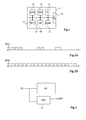
- the figure 1 is a block diagram of an embodiment of an integrated circuit 1 of the type to which the present invention applies.
- a circuit generally comprises a processing unit 11 (PU), one or more memories 12, 13 and 14 among which, for example, a random access memory (RAM) or processing registers, one or more non-volatile memories (NVM) rewritable, one or more non-volatile memories non-rewritable (ROM).
- the circuit 1 comprises one or more bus 15 commands, addresses and data for the various components communicate with each other and an interface 16 input / output (I / O) for communication with the outside of the circuit 1.
- the circuit 1 comprises other components or circuits to implement other functions (symbolized by a block 17, FCT).
- the circuit 1 comprises in particular a crypto-processor 18 (CP) responsible for executing functions implementing secret (key) quantities, for example , encryption, decryption, scrambling, signature calculation functions, etc.
- CP crypto-processor 18
- the integrated circuit whose activity is to be monitored comprises a memory and a crypto-processor (without a central processing unit).
- the invention will be described later in connection with an example of application to the monitoring of a cryptographic activity of the circuit to detect possible attacks. However, it applies more generally to the monitoring of an activity of a component or of any circuit which one wishes to check the frequency of occurrences of an operation with respect to a threshold. For example, it may be to check the frequency of erase-programming operations of a non-volatile memory to, if necessary, postpone certain operations erase-programming to reduce the stress (stress) brought to the memory and improve its life.
- the Figures 2A and 2B are timing diagrams illustrating the activation periods (symbolized arbitrarily by a state 1) and rest periods (symbolized arbitrarily by a state 0) of a signal EN to be monitored.
- the signal EN is the activation signal of a cryptographic function.
- it is a status signal indicating that such a function is active.
- the Figure 2A illustrates a normal operation in which the operation is performed one or more times with relatively long periods of inactivity.
- the periods of inactivity are greater than the periods of activity, the remaining time used for the rest of the circuit to exploit the data provided by this function.
- the Figure 2B illustrates the appearance of the signal EN in the presence of abnormal operation (for example, in the presence of attacks).
- the frequency of repetition of the cryptographic operations is much higher and, above all, the operations are not separated by rest periods. This is because an attacker has the cryptography operation performed with successive assumptions on the data and / or keys and resets the circuit without waiting for this data to be processed further.
- the attack consists in monitoring the consumption of the circuit during the execution of the cryptographic process so as to deduce information on the keys. Resetting the circuit immediately to show other data or assumptions may also prevent a countermeasure being triggered.
- the figure 3 is a block diagram of an embodiment of the present invention. It is assumed that it is desired to monitor an OP operation, for example implemented by block 18 of the figure 1 . It is assumed that the operation whose flow is to be monitored receives an activation signal EN. This activation signal is taken to be sent on a monitoring circuit 2 (SPY) providing a signal DET indicative of a possible abnormal operation. Alternatively, the state signal EN is taken within the OP function. The circuit 2 analyzes the frequency of the periods of activation of the signal EN with respect to a threshold to be able to detect an abnormal operation.
- SPY monitoring circuit 2
- the circuit 2 analyzes the frequency of the periods of activation of the signal EN with respect to a threshold to be able to detect an abnormal operation.
- NBTI negative-biased temperature instability
- V T threshold voltage
- This phenomenon is used here to cause degradation of a detection transistor during the periods when the function to be monitored is active. We then take advantage of the fact that the transistor returns to its normal state (not degraded) after a time that depends, inter alia, the extent of degradation suffered.
- the NBTI phenomenon is known in the art. It is described, for example, in the article " Negative bias temperature instability: Dieter K. Schroder and Jeff A. Babcock's Road to Cross in Deep Submicron Silicon Semiconductor Manufacturing, published in Journal of Applied Physics, 94, pp.1-18, in July 2003 and in the article " A comprehensive model of PMOS NBTI degradation "by M. Alam and S. Mahapatra, published in Microelectronics Reliability, Volume 45, No. 1, pp. 71-81, January 2005 .
- the figure 4 is a detailed circuit diagram of a detection circuit 2 as illustrated in FIG. figure 3 .
- the principle is to compare the behavior of a MOS P1 P-channel transistor which will be subjected to NBTI degradation during the activation periods of the function to be monitored, compared to a P2 transistor also P channel but not subject degradation during these periods.
- two branches 21 and 22, in parallel between two terminals 23 and 24 for applying a positive supply voltage Vdd, each comprise, in series, one of the transistors P1 or P2, a switch (for example , an N-channel transistor N1, respectively N2, and a resistive element R1, respectively R2.
- the branch 22 further comprises, between the transistor P2 and the terminal 23, a switch (for example, a P-channel MOS transistor P5) controlled by the signal EN of activation of the function to be monitored.
- the gates of the transistors N1 and N2 receive the inverse (inverter 25) of the signal EN of activation of the function.
- the interconnection nodes 26 between the transistor N1 and the resistor R1, and 27 between the transistor N2 and the resistor R2, therefore the sources of the transistors N1 and N2, are connected at the input of a comparator 28 (COMP) providing the result DET detection.
- the comparator 28 indirectly compares information relating to the saturation current of the transistors P1 and P2.
- a third branch 29 comprising, in series between the terminals 23 and 24, a switch (for example, a P-channel MOS transistor P6) controlled by the signal EN, a channel transistor P3.
- a switch for example, a P-channel MOS transistor P6 controlled by the signal EN, a channel transistor P3.
- P and a current source 30 the transistor P3 being diode-mounted (gate and drain connected) and its gate being connected to the respective gates of the transistors P1 and P2.
- the polarization branch 29 is controllable by an N-channel MOS transistor N3 connecting the drain of the transistor P3 (connected to the current source 30) to the ground 24.
- the gate of the transistor N3 receives the activation signal EN.
- a transistor N4 whose gate also receives the signal EN, connects the drain of transistor P2 to ground.
- the measuring transistor P1 is placed in a degradation phase by means of a P-channel MOS transistor P4 which bypasses its source and its drain when the signal EN is in the high state.
- the gate of the transistor P4 is connected to the output of the inverter 25.
- the box (bulk) of the transistor P2 as that of all the P-channel transistors of the assembly is, by construction, connected to its source (and therefore to the potential Vdd).
- FIGS. 5A, 5B, 5C and 5D are chronograms illustrating the operation of the circuit of the figure 4 .
- the Figure 5A illustrates an example of the pace of the signal EN to be monitored.
- the Figures 5B and 5C illustrate the respective speeds of the voltages V MES and V REF of the respective drains of the transistors P1 and P2.
- the figure 5D illustrates the pace of the signal DET provided by the amplifier 28.
- the source, box and drain of the transistor P1 are at the potential Vdd (neglecting the voltage drop in the transistor P4 in the on state) , while his grid is at the mass.
- Transistor P1 is then placed under NBTI degradation conditions and charges accumulate in its gate oxide.
- the accumulation of charges which occurred while the transistor P1 was blocked results in a lower current in the transistor, hence a voltage V MES lower than a nominal level V1 (the resistor R1 being fixed).
- the voltage V REF takes a value V2 conditioned by the value of the resistance R2.
- Levels V1 and V2 are not necessarily identical. This depends on whether the switching threshold, that is to say the difference in level between the voltages V MES and V REF (or vice versa) of the comparator 28 is set by an offset (offset) internal to it or by the values of the resistors R1 and R2. Since the voltage V REF does not vary during the measurement periods, the threshold corresponds to a value TH of the voltage V MES below which it is considered that the transistor P1 has accumulated a sufficient degradation to consider an abnormal operation.
- the right part of the timing diagrams illustrates an abnormal operation of the circuit, for example a hacking attempt.
- the periods of activation of the signal EN are very close together. It follows that transistor P1 does not have time to return to its nominal state.
- time t4 the accumulation of charges in the gate oxide of the transistor P1 is such that the voltage V MES passes below the threshold TH, the comparator 28 switches (signal DET, figure 5D ).
- the exploitation of the signal DET can be a blocking of the circuit, the activation of a command, the fact to postpone another action (for example in the case of the writing in nonvolatile memories), etc.
- An advantage of the embodiments described is that it is now possible to take into account the frequency of the activation periods of the circuit and not only their number.
- Another advantage is that the degradation of the transistor P1 is independent of any noise or disturbance of the supply voltage (the two conduction terminals - drain and source - of the transistor P1 are brought to the same potential during the degradation phases). Moreover, this degradation is insensitive to possible attacks of different nature, for example to laser attacks.
- Another advantage is that it is no longer necessary to make successive writes in EEPROM memory, which reduces the stress of this memory.
- Another advantage is that the detection circuit takes up little space. Several circuits 2 can therefore be assigned, in the same electronic circuit, monitoring different activation signals depending on the application.
Landscapes
- Engineering & Computer Science (AREA)
- Computer Security & Cryptography (AREA)
- Computer Networks & Wireless Communication (AREA)
- Signal Processing (AREA)
- Electronic Switches (AREA)
- Logic Circuits (AREA)
- Semiconductor Integrated Circuits (AREA)
- Storage Device Security (AREA)
Applications Claiming Priority (1)
| Application Number | Priority Date | Filing Date | Title |
|---|---|---|---|
| FR0955634A FR2949163B1 (fr) | 2009-08-12 | 2009-08-12 | Surveillance de l'activite d'un circuit electronique |
Publications (3)
| Publication Number | Publication Date |
|---|---|
| EP2285038A2 true EP2285038A2 (de) | 2011-02-16 |
| EP2285038A3 EP2285038A3 (de) | 2011-05-18 |
| EP2285038B1 EP2285038B1 (de) | 2014-10-15 |
Family
ID=42194807
Family Applications (1)
| Application Number | Title | Priority Date | Filing Date |
|---|---|---|---|
| EP10170718.0A Active EP2285038B1 (de) | 2009-08-12 | 2010-07-23 | Überwachung des Aktivitäts einer elektronischer Schaltkreis |
Country Status (5)
| Country | Link |
|---|---|
| US (1) | US8564324B2 (de) |
| EP (1) | EP2285038B1 (de) |
| JP (1) | JP5581147B2 (de) |
| CN (1) | CN101996125B (de) |
| FR (1) | FR2949163B1 (de) |
Cited By (1)
| Publication number | Priority date | Publication date | Assignee | Title |
|---|---|---|---|---|
| WO2017216522A1 (en) * | 2016-06-17 | 2017-12-21 | Arm Ltd | An apparatus and method for obfuscating power consumption of a processor |
Families Citing this family (7)
| Publication number | Priority date | Publication date | Assignee | Title |
|---|---|---|---|---|
| US8892903B1 (en) * | 2012-12-06 | 2014-11-18 | Xilinx, Inc. | Detection of power analysis attacks |
| CN103197717B (zh) * | 2013-02-28 | 2015-11-25 | 华为技术有限公司 | 自适应电压调整方法、芯片以及系统 |
| KR102341264B1 (ko) * | 2015-02-02 | 2021-12-20 | 삼성전자주식회사 | 래치를 이용한 레이저 검출기 및 이를 포함하는 반도체 장치 |
| KR20170061418A (ko) | 2015-11-26 | 2017-06-05 | 삼성전자주식회사 | 스트레스 인가 모드를 갖는 캘리브레이션 회로 및 이를 포함하는 메모리 장치 |
| FR3045184B1 (fr) * | 2015-12-15 | 2018-07-20 | Idemia France | Procede d’ecriture dans une memoire non-volatile d’une entite electronique et entite electronique associee |
| CN105759190B (zh) * | 2016-02-23 | 2018-09-28 | 工业和信息化部电子第五研究所 | Mos管参数退化的检测电路 |
| US10725089B1 (en) * | 2019-08-26 | 2020-07-28 | Nanya Technology Corporation | Semiconductor device and operating method thereof |
Family Cites Families (11)
| Publication number | Priority date | Publication date | Assignee | Title |
|---|---|---|---|---|
| JPS5950139B2 (ja) * | 1978-12-20 | 1984-12-06 | 三菱電機株式会社 | 頻度計数回路 |
| DE10044837C1 (de) * | 2000-09-11 | 2001-09-13 | Infineon Technologies Ag | Schaltungsanordnung und Verfahren zum Detektieren eines unerwünschten Angriffs auf eine integrierte Schaltung |
| FR2813972B1 (fr) * | 2000-09-14 | 2003-12-12 | St Microelectronics Sa | Procede de brouillage de la consommation electrique d'un circuit integre |
| JP2003078018A (ja) * | 2001-08-31 | 2003-03-14 | Sony Corp | 半導体装置 |
| FR2835947A1 (fr) * | 2002-02-11 | 2003-08-15 | St Microelectronics Sa | Extraction d'un code binaire a partir de parametres physiques d'un circuit integre |
| JP2006054499A (ja) * | 2002-07-09 | 2006-02-23 | Renesas Technology Corp | 半導体集積回路装置及びそれを用いた半導体システム |
| WO2006046300A1 (ja) * | 2004-10-29 | 2006-05-04 | Spansion Llc | 半導体装置及び半導体装置の制御方法 |
| JP4437541B2 (ja) * | 2004-11-17 | 2010-03-24 | 富士通マイクロエレクトロニクス株式会社 | リセット制御回路及びリセット制御方法 |
| JP4646615B2 (ja) * | 2004-12-14 | 2011-03-09 | 株式会社リコー | 半導体装置 |
| JP2008028833A (ja) * | 2006-07-24 | 2008-02-07 | Sharp Corp | 半導体集積回路 |
| JP2009157536A (ja) * | 2007-12-25 | 2009-07-16 | Toshiba Corp | 情報処理装置 |
-
2009
- 2009-08-12 FR FR0955634A patent/FR2949163B1/fr not_active Expired - Fee Related
-
2010
- 2010-07-23 EP EP10170718.0A patent/EP2285038B1/de active Active
- 2010-08-10 CN CN201010252651.1A patent/CN101996125B/zh active Active
- 2010-08-10 US US12/853,606 patent/US8564324B2/en active Active
- 2010-08-11 JP JP2010180256A patent/JP5581147B2/ja active Active
Non-Patent Citations (2)
| Title |
|---|
| DIETER K. SCHRODER; JEFF A. BABCOCK, JOURNAL OF APPLIED PHYSICS, vol. 94, July 2003 (2003-07-01), pages 1 - 18 |
| M. ALAM; S. MAHAPATRA: "A comprehensive model of PMOS NBTI degradation", MICROELECTRONICS RELIABILITY, vol. 45, no. 1, January 2005 (2005-01-01), pages 71 - 81 |
Cited By (2)
| Publication number | Priority date | Publication date | Assignee | Title |
|---|---|---|---|---|
| WO2017216522A1 (en) * | 2016-06-17 | 2017-12-21 | Arm Ltd | An apparatus and method for obfuscating power consumption of a processor |
| US10255462B2 (en) | 2016-06-17 | 2019-04-09 | Arm Limited | Apparatus and method for obfuscating power consumption of a processor |
Also Published As
| Publication number | Publication date |
|---|---|
| JP2011041280A (ja) | 2011-02-24 |
| EP2285038B1 (de) | 2014-10-15 |
| FR2949163A1 (fr) | 2011-02-18 |
| JP5581147B2 (ja) | 2014-08-27 |
| CN101996125A (zh) | 2011-03-30 |
| CN101996125B (zh) | 2015-10-14 |
| EP2285038A3 (de) | 2011-05-18 |
| FR2949163B1 (fr) | 2011-12-09 |
| US20110128030A1 (en) | 2011-06-02 |
| US8564324B2 (en) | 2013-10-22 |
Similar Documents
| Publication | Publication Date | Title |
|---|---|---|
| EP2285038B1 (de) | Überwachung des Aktivitäts einer elektronischer Schaltkreis | |
| EP2280364A1 (de) | Fehlerinjektionsdetektor in einer integrierten Schaltung | |
| FR2660457A1 (fr) | Circuit de protection contre l'effacement et la programmation d'une memoire remanente. | |
| EP2108164B1 (de) | Einschränkung des zugriffs auf eine elektronische schaltung | |
| FR2667169A1 (fr) | Circuit de production de haute tension pour un circuit de memoire a semiconducteur. | |
| EP0453351B1 (de) | Sicherungsdetektorschaltung | |
| EP0298848A2 (de) | Elektronischer Detektor für einen binären logischen Pegel | |
| FR2959580A1 (fr) | Circuit et procede de detection d'une attaque par injection de fautes | |
| EP2108163A1 (de) | Schutz von in einer elektronischen schaltung enthaltenen informationen | |
| EP1993057A1 (de) | Erkennung einer Zustandsstörung eines bistabilen Kippschalters eines elektronischen Schaltkreises | |
| FR2916560A1 (fr) | Cryptoprocesseur a protection de donnees amelioree | |
| EP1220101B1 (de) | Verfahren und Vorrichtung zum Schutz gegen unbefugte Benutzung eines integrierten Schaltkreises | |
| EP3264460A1 (de) | Verfahren zum schutz eines integrierten schaltkreises, und entsprechender integrierter schaltkreis | |
| FR2935059A1 (fr) | Procede de detection d'anomalies dans un circuit de cryptographie protege par logique differentielle et circuit mettant en oeuvre un tel procede | |
| EP2108165A1 (de) | Vorübergehende sperrung einer elektronischen schaltung | |
| EP0884704B1 (de) | Beglaubigungsverfahren für integrierte Schaltung | |
| EP1346508A1 (de) | Logisher schaltkreis mit variablen internen polaritäten | |
| EP1633074A1 (de) | Integrierte Schaltung mit kodiertem Sicherungsignal, Sicherungsverfahren, Vorrichtung und mittels eines entsprechenden dynamischen Schlüssels kodiertes Sicherungsignal | |
| FR2802733A1 (fr) | Bascule de type d maitre-esclave securisee | |
| EP1295297B1 (de) | Verwendungserkennungsschaltung | |
| FR2534751A1 (fr) | Circuit de restauration a la mise sous tension pour un systeme de commande electrique | |
| EP1168621A1 (de) | Integrierte Schaltung mit Schutzvorrichtung | |
| WO2001084491A2 (fr) | Procede de contre mesure dans un microcircuit et carte a puce comportant ledit microcircuit | |
| EP1400887A1 (de) | Schutzgerät für einen elektronischen Chip, der vertaulichen Informationen enthält | |
| FR3070092A1 (fr) | Protection d'un circuit integre |
Legal Events
| Date | Code | Title | Description |
|---|---|---|---|
| PUAI | Public reference made under article 153(3) epc to a published international application that has entered the european phase |
Free format text: ORIGINAL CODE: 0009012 |
|
| 17P | Request for examination filed |
Effective date: 20100723 |
|
| AK | Designated contracting states |
Kind code of ref document: A2 Designated state(s): AL AT BE BG CH CY CZ DE DK EE ES FI FR GB GR HR HU IE IS IT LI LT LU LV MC MK MT NL NO PL PT RO SE SI SK SM TR |
|
| AX | Request for extension of the european patent |
Extension state: BA ME RS |
|
| PUAL | Search report despatched |
Free format text: ORIGINAL CODE: 0009013 |
|
| AK | Designated contracting states |
Kind code of ref document: A3 Designated state(s): AL AT BE BG CH CY CZ DE DK EE ES FI FR GB GR HR HU IE IS IT LI LT LU LV MC MK MT NL NO PL PT RO SE SI SK SM TR |
|
| AX | Request for extension of the european patent |
Extension state: BA ME RS |
|
| REG | Reference to a national code |
Ref country code: DE Ref legal event code: R079 Ref document number: 602010019520 Country of ref document: DE Free format text: PREVIOUS MAIN CLASS: H04L0009060000 Ipc: H04L0009000000 |
|
| RIC1 | Information provided on ipc code assigned before grant |
Ipc: H04L 9/00 20060101AFI20140109BHEP |
|
| GRAP | Despatch of communication of intention to grant a patent |
Free format text: ORIGINAL CODE: EPIDOSNIGR1 |
|
| INTG | Intention to grant announced |
Effective date: 20140513 |
|
| GRAS | Grant fee paid |
Free format text: ORIGINAL CODE: EPIDOSNIGR3 |
|
| GRAA | (expected) grant |
Free format text: ORIGINAL CODE: 0009210 |
|
| AK | Designated contracting states |
Kind code of ref document: B1 Designated state(s): AL AT BE BG CH CY CZ DE DK EE ES FI FR GB GR HR HU IE IS IT LI LT LU LV MC MK MT NL NO PL PT RO SE SI SK SM TR |
|
| REG | Reference to a national code |
Ref country code: CH Ref legal event code: EP Ref country code: GB Ref legal event code: FG4D Free format text: NOT ENGLISH |
|
| REG | Reference to a national code |
Ref country code: IE Ref legal event code: FG4D Free format text: LANGUAGE OF EP DOCUMENT: FRENCH |
|
| REG | Reference to a national code |
Ref country code: AT Ref legal event code: REF Ref document number: 692067 Country of ref document: AT Kind code of ref document: T Effective date: 20141115 |
|
| REG | Reference to a national code |
Ref country code: DE Ref legal event code: R096 Ref document number: 602010019520 Country of ref document: DE Effective date: 20141127 |
|
| REG | Reference to a national code |
Ref country code: NL Ref legal event code: VDEP Effective date: 20141015 |
|
| REG | Reference to a national code |
Ref country code: AT Ref legal event code: MK05 Ref document number: 692067 Country of ref document: AT Kind code of ref document: T Effective date: 20141015 |
|
| REG | Reference to a national code |
Ref country code: LT Ref legal event code: MG4D |
|
| PG25 | Lapsed in a contracting state [announced via postgrant information from national office to epo] |
Ref country code: NL Free format text: LAPSE BECAUSE OF FAILURE TO SUBMIT A TRANSLATION OF THE DESCRIPTION OR TO PAY THE FEE WITHIN THE PRESCRIBED TIME-LIMIT Effective date: 20141015 |
|
| PG25 | Lapsed in a contracting state [announced via postgrant information from national office to epo] |
Ref country code: IS Free format text: LAPSE BECAUSE OF FAILURE TO SUBMIT A TRANSLATION OF THE DESCRIPTION OR TO PAY THE FEE WITHIN THE PRESCRIBED TIME-LIMIT Effective date: 20150215 Ref country code: PT Free format text: LAPSE BECAUSE OF FAILURE TO SUBMIT A TRANSLATION OF THE DESCRIPTION OR TO PAY THE FEE WITHIN THE PRESCRIBED TIME-LIMIT Effective date: 20150216 Ref country code: ES Free format text: LAPSE BECAUSE OF FAILURE TO SUBMIT A TRANSLATION OF THE DESCRIPTION OR TO PAY THE FEE WITHIN THE PRESCRIBED TIME-LIMIT Effective date: 20141015 Ref country code: LT Free format text: LAPSE BECAUSE OF FAILURE TO SUBMIT A TRANSLATION OF THE DESCRIPTION OR TO PAY THE FEE WITHIN THE PRESCRIBED TIME-LIMIT Effective date: 20141015 Ref country code: NO Free format text: LAPSE BECAUSE OF FAILURE TO SUBMIT A TRANSLATION OF THE DESCRIPTION OR TO PAY THE FEE WITHIN THE PRESCRIBED TIME-LIMIT Effective date: 20150115 Ref country code: FI Free format text: LAPSE BECAUSE OF FAILURE TO SUBMIT A TRANSLATION OF THE DESCRIPTION OR TO PAY THE FEE WITHIN THE PRESCRIBED TIME-LIMIT Effective date: 20141015 |
|
| PG25 | Lapsed in a contracting state [announced via postgrant information from national office to epo] |
Ref country code: LV Free format text: LAPSE BECAUSE OF FAILURE TO SUBMIT A TRANSLATION OF THE DESCRIPTION OR TO PAY THE FEE WITHIN THE PRESCRIBED TIME-LIMIT Effective date: 20141015 Ref country code: CY Free format text: LAPSE BECAUSE OF FAILURE TO SUBMIT A TRANSLATION OF THE DESCRIPTION OR TO PAY THE FEE WITHIN THE PRESCRIBED TIME-LIMIT Effective date: 20141015 Ref country code: SE Free format text: LAPSE BECAUSE OF FAILURE TO SUBMIT A TRANSLATION OF THE DESCRIPTION OR TO PAY THE FEE WITHIN THE PRESCRIBED TIME-LIMIT Effective date: 20141015 Ref country code: HR Free format text: LAPSE BECAUSE OF FAILURE TO SUBMIT A TRANSLATION OF THE DESCRIPTION OR TO PAY THE FEE WITHIN THE PRESCRIBED TIME-LIMIT Effective date: 20141015 Ref country code: AT Free format text: LAPSE BECAUSE OF FAILURE TO SUBMIT A TRANSLATION OF THE DESCRIPTION OR TO PAY THE FEE WITHIN THE PRESCRIBED TIME-LIMIT Effective date: 20141015 Ref country code: GR Free format text: LAPSE BECAUSE OF FAILURE TO SUBMIT A TRANSLATION OF THE DESCRIPTION OR TO PAY THE FEE WITHIN THE PRESCRIBED TIME-LIMIT Effective date: 20150116 Ref country code: PL Free format text: LAPSE BECAUSE OF FAILURE TO SUBMIT A TRANSLATION OF THE DESCRIPTION OR TO PAY THE FEE WITHIN THE PRESCRIBED TIME-LIMIT Effective date: 20141015 |
|
| REG | Reference to a national code |
Ref country code: DE Ref legal event code: R097 Ref document number: 602010019520 Country of ref document: DE |
|
| PG25 | Lapsed in a contracting state [announced via postgrant information from national office to epo] |
Ref country code: RO Free format text: LAPSE BECAUSE OF FAILURE TO SUBMIT A TRANSLATION OF THE DESCRIPTION OR TO PAY THE FEE WITHIN THE PRESCRIBED TIME-LIMIT Effective date: 20141015 Ref country code: CZ Free format text: LAPSE BECAUSE OF FAILURE TO SUBMIT A TRANSLATION OF THE DESCRIPTION OR TO PAY THE FEE WITHIN THE PRESCRIBED TIME-LIMIT Effective date: 20141015 Ref country code: EE Free format text: LAPSE BECAUSE OF FAILURE TO SUBMIT A TRANSLATION OF THE DESCRIPTION OR TO PAY THE FEE WITHIN THE PRESCRIBED TIME-LIMIT Effective date: 20141015 Ref country code: SK Free format text: LAPSE BECAUSE OF FAILURE TO SUBMIT A TRANSLATION OF THE DESCRIPTION OR TO PAY THE FEE WITHIN THE PRESCRIBED TIME-LIMIT Effective date: 20141015 Ref country code: DK Free format text: LAPSE BECAUSE OF FAILURE TO SUBMIT A TRANSLATION OF THE DESCRIPTION OR TO PAY THE FEE WITHIN THE PRESCRIBED TIME-LIMIT Effective date: 20141015 |
|
| PLBE | No opposition filed within time limit |
Free format text: ORIGINAL CODE: 0009261 |
|
| STAA | Information on the status of an ep patent application or granted ep patent |
Free format text: STATUS: NO OPPOSITION FILED WITHIN TIME LIMIT |
|
| PG25 | Lapsed in a contracting state [announced via postgrant information from national office to epo] |
Ref country code: IT Free format text: LAPSE BECAUSE OF FAILURE TO SUBMIT A TRANSLATION OF THE DESCRIPTION OR TO PAY THE FEE WITHIN THE PRESCRIBED TIME-LIMIT Effective date: 20141015 |
|
| 26N | No opposition filed |
Effective date: 20150716 |
|
| PG25 | Lapsed in a contracting state [announced via postgrant information from national office to epo] |
Ref country code: MC Free format text: LAPSE BECAUSE OF FAILURE TO SUBMIT A TRANSLATION OF THE DESCRIPTION OR TO PAY THE FEE WITHIN THE PRESCRIBED TIME-LIMIT Effective date: 20141015 Ref country code: SI Free format text: LAPSE BECAUSE OF FAILURE TO SUBMIT A TRANSLATION OF THE DESCRIPTION OR TO PAY THE FEE WITHIN THE PRESCRIBED TIME-LIMIT Effective date: 20141015 |
|
| REG | Reference to a national code |
Ref country code: CH Ref legal event code: PL |
|
| GBPC | Gb: european patent ceased through non-payment of renewal fee |
Effective date: 20150723 |
|
| PG25 | Lapsed in a contracting state [announced via postgrant information from national office to epo] |
Ref country code: LU Free format text: LAPSE BECAUSE OF FAILURE TO SUBMIT A TRANSLATION OF THE DESCRIPTION OR TO PAY THE FEE WITHIN THE PRESCRIBED TIME-LIMIT Effective date: 20150723 |
|
| REG | Reference to a national code |
Ref country code: IE Ref legal event code: MM4A |
|
| PG25 | Lapsed in a contracting state [announced via postgrant information from national office to epo] |
Ref country code: LI Free format text: LAPSE BECAUSE OF NON-PAYMENT OF DUE FEES Effective date: 20150731 Ref country code: CH Free format text: LAPSE BECAUSE OF NON-PAYMENT OF DUE FEES Effective date: 20150731 Ref country code: GB Free format text: LAPSE BECAUSE OF NON-PAYMENT OF DUE FEES Effective date: 20150723 |
|
| REG | Reference to a national code |
Ref country code: FR Ref legal event code: PLFP Year of fee payment: 7 |
|
| PG25 | Lapsed in a contracting state [announced via postgrant information from national office to epo] |
Ref country code: IE Free format text: LAPSE BECAUSE OF NON-PAYMENT OF DUE FEES Effective date: 20150723 |
|
| PG25 | Lapsed in a contracting state [announced via postgrant information from national office to epo] |
Ref country code: MT Free format text: LAPSE BECAUSE OF FAILURE TO SUBMIT A TRANSLATION OF THE DESCRIPTION OR TO PAY THE FEE WITHIN THE PRESCRIBED TIME-LIMIT Effective date: 20141015 |
|
| PG25 | Lapsed in a contracting state [announced via postgrant information from national office to epo] |
Ref country code: BG Free format text: LAPSE BECAUSE OF FAILURE TO SUBMIT A TRANSLATION OF THE DESCRIPTION OR TO PAY THE FEE WITHIN THE PRESCRIBED TIME-LIMIT Effective date: 20141015 Ref country code: HU Free format text: LAPSE BECAUSE OF FAILURE TO SUBMIT A TRANSLATION OF THE DESCRIPTION OR TO PAY THE FEE WITHIN THE PRESCRIBED TIME-LIMIT; INVALID AB INITIO Effective date: 20100723 Ref country code: SM Free format text: LAPSE BECAUSE OF FAILURE TO SUBMIT A TRANSLATION OF THE DESCRIPTION OR TO PAY THE FEE WITHIN THE PRESCRIBED TIME-LIMIT Effective date: 20141015 |
|
| REG | Reference to a national code |
Ref country code: FR Ref legal event code: PLFP Year of fee payment: 8 |
|
| PG25 | Lapsed in a contracting state [announced via postgrant information from national office to epo] |
Ref country code: BE Free format text: LAPSE BECAUSE OF NON-PAYMENT OF DUE FEES Effective date: 20150731 |
|
| PG25 | Lapsed in a contracting state [announced via postgrant information from national office to epo] |
Ref country code: TR Free format text: LAPSE BECAUSE OF FAILURE TO SUBMIT A TRANSLATION OF THE DESCRIPTION OR TO PAY THE FEE WITHIN THE PRESCRIBED TIME-LIMIT Effective date: 20141015 |
|
| REG | Reference to a national code |
Ref country code: FR Ref legal event code: PLFP Year of fee payment: 9 |
|
| PG25 | Lapsed in a contracting state [announced via postgrant information from national office to epo] |
Ref country code: MK Free format text: LAPSE BECAUSE OF FAILURE TO SUBMIT A TRANSLATION OF THE DESCRIPTION OR TO PAY THE FEE WITHIN THE PRESCRIBED TIME-LIMIT Effective date: 20141015 |
|
| PG25 | Lapsed in a contracting state [announced via postgrant information from national office to epo] |
Ref country code: AL Free format text: LAPSE BECAUSE OF FAILURE TO SUBMIT A TRANSLATION OF THE DESCRIPTION OR TO PAY THE FEE WITHIN THE PRESCRIBED TIME-LIMIT Effective date: 20141015 |
|
| PGFP | Annual fee paid to national office [announced via postgrant information from national office to epo] |
Ref country code: FR Payment date: 20190621 Year of fee payment: 10 |
|
| PG25 | Lapsed in a contracting state [announced via postgrant information from national office to epo] |
Ref country code: FR Free format text: LAPSE BECAUSE OF NON-PAYMENT OF DUE FEES Effective date: 20200731 |
|
| PGFP | Annual fee paid to national office [announced via postgrant information from national office to epo] |
Ref country code: DE Payment date: 20230620 Year of fee payment: 14 |