EP2278866B1 - Tableau de connexions rigide et flexible - Google Patents
Tableau de connexions rigide et flexible Download PDFInfo
- Publication number
- EP2278866B1 EP2278866B1 EP10186158A EP10186158A EP2278866B1 EP 2278866 B1 EP2278866 B1 EP 2278866B1 EP 10186158 A EP10186158 A EP 10186158A EP 10186158 A EP10186158 A EP 10186158A EP 2278866 B1 EP2278866 B1 EP 2278866B1
- Authority
- EP
- European Patent Office
- Prior art keywords
- flexible substrate
- flex
- board
- rigid
- insulating layer
- Prior art date
- Legal status (The legal status is an assumption and is not a legal conclusion. Google has not performed a legal analysis and makes no representation as to the accuracy of the status listed.)
- Not-in-force
Links
Images


Classifications
-
- H—ELECTRICITY
- H05—ELECTRIC TECHNIQUES NOT OTHERWISE PROVIDED FOR
- H05K—PRINTED CIRCUITS; CASINGS OR CONSTRUCTIONAL DETAILS OF ELECTRIC APPARATUS; MANUFACTURE OF ASSEMBLAGES OF ELECTRICAL COMPONENTS
- H05K3/00—Apparatus or processes for manufacturing printed circuits
- H05K3/46—Manufacturing multilayer circuits
- H05K3/4644—Manufacturing multilayer circuits by building the multilayer layer by layer, i.e. build-up multilayer circuits
-
- H—ELECTRICITY
- H05—ELECTRIC TECHNIQUES NOT OTHERWISE PROVIDED FOR
- H05K—PRINTED CIRCUITS; CASINGS OR CONSTRUCTIONAL DETAILS OF ELECTRIC APPARATUS; MANUFACTURE OF ASSEMBLAGES OF ELECTRICAL COMPONENTS
- H05K3/00—Apparatus or processes for manufacturing printed circuits
- H05K3/46—Manufacturing multilayer circuits
-
- H—ELECTRICITY
- H05—ELECTRIC TECHNIQUES NOT OTHERWISE PROVIDED FOR
- H05K—PRINTED CIRCUITS; CASINGS OR CONSTRUCTIONAL DETAILS OF ELECTRIC APPARATUS; MANUFACTURE OF ASSEMBLAGES OF ELECTRICAL COMPONENTS
- H05K1/00—Printed circuits
- H05K1/02—Details
-
- H—ELECTRICITY
- H05—ELECTRIC TECHNIQUES NOT OTHERWISE PROVIDED FOR
- H05K—PRINTED CIRCUITS; CASINGS OR CONSTRUCTIONAL DETAILS OF ELECTRIC APPARATUS; MANUFACTURE OF ASSEMBLAGES OF ELECTRICAL COMPONENTS
- H05K3/00—Apparatus or processes for manufacturing printed circuits
- H05K3/46—Manufacturing multilayer circuits
- H05K3/4688—Composite multilayer circuits, i.e. comprising insulating layers having different properties
- H05K3/4691—Rigid-flexible multilayer circuits comprising rigid and flexible layers, e.g. having in the bending regions only flexible layers
-
- H—ELECTRICITY
- H05—ELECTRIC TECHNIQUES NOT OTHERWISE PROVIDED FOR
- H05K—PRINTED CIRCUITS; CASINGS OR CONSTRUCTIONAL DETAILS OF ELECTRIC APPARATUS; MANUFACTURE OF ASSEMBLAGES OF ELECTRICAL COMPONENTS
- H05K2201/00—Indexing scheme relating to printed circuits covered by H05K1/00
- H05K2201/01—Dielectrics
- H05K2201/0183—Dielectric layers
- H05K2201/0187—Dielectric layers with regions of different dielectrics in the same layer, e.g. in a printed capacitor for locally changing the dielectric properties
-
- H—ELECTRICITY
- H05—ELECTRIC TECHNIQUES NOT OTHERWISE PROVIDED FOR
- H05K—PRINTED CIRCUITS; CASINGS OR CONSTRUCTIONAL DETAILS OF ELECTRIC APPARATUS; MANUFACTURE OF ASSEMBLAGES OF ELECTRICAL COMPONENTS
- H05K2201/00—Indexing scheme relating to printed circuits covered by H05K1/00
- H05K2201/09—Shape and layout
- H05K2201/09009—Substrate related
- H05K2201/09127—PCB or component having an integral separable or breakable part
-
- H—ELECTRICITY
- H05—ELECTRIC TECHNIQUES NOT OTHERWISE PROVIDED FOR
- H05K—PRINTED CIRCUITS; CASINGS OR CONSTRUCTIONAL DETAILS OF ELECTRIC APPARATUS; MANUFACTURE OF ASSEMBLAGES OF ELECTRICAL COMPONENTS
- H05K2201/00—Indexing scheme relating to printed circuits covered by H05K1/00
- H05K2201/09—Shape and layout
- H05K2201/09209—Shape and layout details of conductors
- H05K2201/095—Conductive through-holes or vias
- H05K2201/09509—Blind vias, i.e. vias having one side closed
-
- H—ELECTRICITY
- H05—ELECTRIC TECHNIQUES NOT OTHERWISE PROVIDED FOR
- H05K—PRINTED CIRCUITS; CASINGS OR CONSTRUCTIONAL DETAILS OF ELECTRIC APPARATUS; MANUFACTURE OF ASSEMBLAGES OF ELECTRICAL COMPONENTS
- H05K2201/00—Indexing scheme relating to printed circuits covered by H05K1/00
- H05K2201/09—Shape and layout
- H05K2201/09209—Shape and layout details of conductors
- H05K2201/095—Conductive through-holes or vias
- H05K2201/09563—Metal filled via
-
- H—ELECTRICITY
- H05—ELECTRIC TECHNIQUES NOT OTHERWISE PROVIDED FOR
- H05K—PRINTED CIRCUITS; CASINGS OR CONSTRUCTIONAL DETAILS OF ELECTRIC APPARATUS; MANUFACTURE OF ASSEMBLAGES OF ELECTRICAL COMPONENTS
- H05K2201/00—Indexing scheme relating to printed circuits covered by H05K1/00
- H05K2201/09—Shape and layout
- H05K2201/09209—Shape and layout details of conductors
- H05K2201/095—Conductive through-holes or vias
- H05K2201/096—Vertically aligned vias, holes or stacked vias
-
- H—ELECTRICITY
- H05—ELECTRIC TECHNIQUES NOT OTHERWISE PROVIDED FOR
- H05K—PRINTED CIRCUITS; CASINGS OR CONSTRUCTIONAL DETAILS OF ELECTRIC APPARATUS; MANUFACTURE OF ASSEMBLAGES OF ELECTRICAL COMPONENTS
- H05K2201/00—Indexing scheme relating to printed circuits covered by H05K1/00
- H05K2201/09—Shape and layout
- H05K2201/09209—Shape and layout details of conductors
- H05K2201/095—Conductive through-holes or vias
- H05K2201/09627—Special connections between adjacent vias, not for grounding vias
-
- H—ELECTRICITY
- H05—ELECTRIC TECHNIQUES NOT OTHERWISE PROVIDED FOR
- H05K—PRINTED CIRCUITS; CASINGS OR CONSTRUCTIONAL DETAILS OF ELECTRIC APPARATUS; MANUFACTURE OF ASSEMBLAGES OF ELECTRICAL COMPONENTS
- H05K3/00—Apparatus or processes for manufacturing printed circuits
- H05K3/0011—Working of insulating substrates or insulating layers
- H05K3/0017—Etching of the substrate by chemical or physical means
- H05K3/0026—Etching of the substrate by chemical or physical means by laser ablation
- H05K3/0032—Etching of the substrate by chemical or physical means by laser ablation of organic insulating material
- H05K3/0035—Etching of the substrate by chemical or physical means by laser ablation of organic insulating material of blind holes, i.e. having a metal layer at the bottom
-
- H—ELECTRICITY
- H05—ELECTRIC TECHNIQUES NOT OTHERWISE PROVIDED FOR
- H05K—PRINTED CIRCUITS; CASINGS OR CONSTRUCTIONAL DETAILS OF ELECTRIC APPARATUS; MANUFACTURE OF ASSEMBLAGES OF ELECTRICAL COMPONENTS
- H05K3/00—Apparatus or processes for manufacturing printed circuits
- H05K3/46—Manufacturing multilayer circuits
- H05K3/4602—Manufacturing multilayer circuits characterized by a special circuit board as base or central core whereon additional circuit layers are built or additional circuit boards are laminated
-
- H—ELECTRICITY
- H05—ELECTRIC TECHNIQUES NOT OTHERWISE PROVIDED FOR
- H05K—PRINTED CIRCUITS; CASINGS OR CONSTRUCTIONAL DETAILS OF ELECTRIC APPARATUS; MANUFACTURE OF ASSEMBLAGES OF ELECTRICAL COMPONENTS
- H05K3/00—Apparatus or processes for manufacturing printed circuits
- H05K3/46—Manufacturing multilayer circuits
- H05K3/4644—Manufacturing multilayer circuits by building the multilayer layer by layer, i.e. build-up multilayer circuits
- H05K3/4652—Adding a circuit layer by laminating a metal foil or a preformed metal foil pattern
Definitions
- the present invention relates to a flexible wiring board partially including a flexible substrate.
- Flex-rigid wiring boards each including a rigid portion and a flexible portion are disclosed in, for example, Unexamined Japanese Parent Application KOKAI Publication No. 2006-140213 , Unexamined Japanese Patent Application KOKAI Publication No. 2006-100703 , International Publication No. WO2004/093508 .
- a flex-rigid wiring board disclosed in Unexamined Japanese Parent Application KOKAI Publication No. 2006-140213 includes a core board provided as a rigid portion, a flexible board disposed adjacent to the core board in the horizontal direction, a flexible adhesive layer laminated on the core board and the flexible board, a wiring pattern formed an the flexible adhesive layer disposed in the rigid portion, and blind vias and/or through holes for connecting wiring patterns formed in respective layers.
- the flexible adhesive layer is laminated on the flexible board, and thus bending stress of the flexible board is large. Therefore, large force is applied to a connection portion between a conductor of the flexible board and a conductor of the rigid board, thereby easily causing disconnection.
- Unexamined Japanese Patent Application KOKAI Publication No. 2006-100703 discloses a method of manufacturing a flex-rigid wiring board.
- a rigid board having a vertical wiring portion formed in a connection region thereof and a flexible board having a connection terminal formed at an end thereof are separately formed.
- the connection region of the rigid board is cut our to a depth larger than the thickness of the flexible board to form a step.
- the connection terminal of the flexible board is connected to the vertical wiring portion of the step.
- connection between conductors of the rigid board and the flexible board becomes weak.
- a flex rigid wiring board disclosed in International Publication No. WO2004/093508 includes a rigid board and a flexible board which are bonded together with an insularing adhesive to form a unified body. Furthermore, connection electrode pass of the rigid board and the flexible board are electrically and physically connected through bulk conductors provided through the insulating adhesive.
- the flexible board is disposed on one of the sides of the rigid substrate, and laser is applied to the flexible board side to form vias for plating connection.
- a bending portion is maintained only on one side, and thus a portion connected by plating has low connection reliability.
- WO 93/11652 discloses a flex-rigid wiring board exhibiting features corresponding to those set forth in the precharacterising portion of Claim 1 below.
- EP 1 566 993 A1 and JP 2006 140213 A are referred to as useful technical background.
- the present invention has been achieved in consideration of the above-described situation, and it is an advantage of embodiments of the present invention to provide a flex-rigid wiring board with high reliability, particularly high connection reliability.
- an insulating layer covers a flexible substrate, thereby defining a conductor pattern of the flexible substrate and a conductor pattern on the insulating layer. Therefore, high connection reliability between the conductor pattern of the flexible substrate and the conductor pattern on the insulating layer can be achieved.
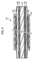
- a flex-rigid wiring board 10 according to an embodiment of the present invention will be described.
- the flex-rigid wiring board 10 includes a first rigid board (rigid board) 11, a second rigid board 12, and a flexible board 13 connecting the rigid boards 11 and 12 to each other.
- first and second rigid boards 11 and 12 On each of first and second rigid boards 11 and 12, any desired circuit pattern is formed. If required, for example, an electronic component such as a semiconductor chip is connected to each board.
- strips-shaped wiring 13a is formed for connecting the circuit patterns on the first and second rigid boards 11 and 12.
- the wiring 13a connects the circuit patterns on the rigid boards 11 and 12 to each other.
- Fig. 2 is an enlarged sectional view of an area denoted by reference numeral 2 in Fig. 1A .
- the flexible board 13 has a structure in which a substrate 131, conductor layers 132 and 133, insulating layers 134 and 135, shield layers 136 and 137, and cover lays 138 and 139 are laminated.
- the substrate 131 is composed of an insulating flexible sheet, for example, a polyimide sheet having a thickness of 20 to 50 ⁇ m and preferably about 30 ⁇ m.
- the conductor layers 132 and 133 are formed on the front and back surfaces of the substrate 131, respectively, and each have a wiring stripe pattern 13a.
- each of the conductor layers 132 and 133 has a copper pattern having a thickness of about 5 to 15 ⁇ m.
- the insulating layers 134 and 135 are composed of a polyimide film having a thickness of about 5 to 15 ⁇ m and insulate the conductor layers 132 and 133, respectively, from the outside.
- the shield layers 136 and 137 are conductive layers each including, for example, a silver paste cured film and shield the conductor layers 132 and 133 from external electromagnetic noise and shield the emission of electromagnetic noise toward the outside.
- the cover lays 138 and 139 include insulating films of polyimide or the like having a thickness of about 5 to 15 ⁇ m and insulate and protect the whole flexible board 13 form the outside.
- the rigid board 11 includes a laminate of a first insulating layer 111, a non-flexible substrate 112, a second insulating layer 113, and first and second upper insulating layers 114 and 115.
- the non-flexible substrate 112 gives rigidity to the rigid board 11 and is composed of a non-flexible insulating material such as a glass epoxy resin.
- the non-flexible substrate 112 is disposed with a space from the flexible board 13 in a horizontal direction.
- the non-flexible substrate 112 has substantially the same thickness as the flexible board 13, for example, 50 to 150 ⁇ m and preferably about 100 ⁇ m.
- Each of the first and second insulating layers 111 and 113 is formed by curing prepreg and has a thickness of 50 to 100 ⁇ m and preferably about 50 ⁇ m.
- the prepreg preferably contains a resin having a low flow characteristic.
- Such prepreg can be prepared by impregnating a glass cloth with an epoxy resin and then thermally curing the resin to increase the degree of curing.
- the prepreg can also be formed by impregnating a glass cloth with a resin with high viscosity, impregnating a glass cloth with a resin containing an inorganic filler, e.g., a silica filler, or impregnating a glass cloth with a decreased amount of resin.
- a resin with high viscosity impregnating a glass cloth with a resin containing an inorganic filler, e.g., a silica filler, or impregnating a glass cloth with a decreased amount of resin.
- an inorganic filler e.g., a silica filler
- the first and second insulating layers 111 and 113 cover both the front and the back surfaces of the non-flexible substrate 112 and the flexible board 13 to partially expose the flexible board 13.
- the resin of the first and second insulating layers 111 and 113 is polymerized with the resin of the cover lays 138 and 139 on the surfaces of the flexible board 13.
- the non-flexible substrate 112 and the first and second insulating layers 111 and 113 constitute the core of the rigid board 11 to support the rigid board 11 and hold one of the ends of the flexible board 13 to support and fix the flexible board 13.
- the spaces formed by the non-flexible substrate 112, the flexible board 13, and the first and second insulating layers 111 and 1113 are filled with a resin 125.
- the resin 125 seeps from the low-flow prepreg constituting the first and second insulating layer 111 and 113, for example, during manufacture.
- the resin 125 is cured integrally with the first and second insulating layers 111 and 113.
- vias (via holes or contact holes) 116 are formed in a portion opposing connection pads 13b of the wiring 133 of the flexible board 13.
- the shield layer 137 and the cover lay 139 of the flexible board 13 are removed from a portion opposing the vias 116 (a portion in which the connection pads 13b of the conductor layer 13a are formed).
- the vias 116 pass through the insulating layer 135 of the flexible board 13 to expose the connection pads 13b of the conductor layer 133.
- a conductor layer 117 is formed on the inner surface of each of the vias 116 by copper plating or the like.
- the wiring pattern 117 is connected by plating to the connection pads 13b of the conductor layer 113 of the flexible board 13.
- the vias 116 are filled with a resin.
- an extraction pattern 118 is formed on the second insulating layer 113 to be connected to the wiring pattern 117.
- the extraction pattern 118 includes a copper plating layer or the like.
- a copper pattern 124 insulated from other components is formed at an end of the second insulating layer 113, i.e., at a position beyond the boundary between the flexible board 13 and the non-flexible substrate 112. Therefore, heat generated in the rigid board 11 can be effectively radiated.
- the first upper insulating layer 114 is laminated on the second insulating layer 113.
- the first upper insulating layer 114 is formed by curing a material containing an inorganic material, for example, prepreg prepared by impregnating a glass cloth with a resin. This can improve the resistance to dropping impact.
- the vias 116 are filled with the resin seeping from the prepreg.
- the second upper insulating layer 115 is disposed on the first upper insulating layer 114.
- the second upper insulating layer 115 is also formed by curing prepreg including a glass cloth impregnated with a resin.
- first upper vias 119 are formed to be connected to the extraction pattern 118.
- the vias 119 are filled with a conductor 120 such as copper or the like.
- second upper via vias (second upper via) 121 are formed to be connected to the vias 119.
- the vias 121 are filled with a conductor 121 such as copper or the like. Namely, the vias 119 and 121 form field built-up vias.
- a conductor pattern (circuit pattern) 123 is appropriately formed on the second upper insulating layer 115.
- the vias 119 are appropriately connected to the conductor pattern 123.
- connection portion between the rigid board 12 and the flexible board 13 is the same as that of the connection portion between the rigid board 11 and the flexible board 13.
- the end of the flexible board 13 is held between the first and second insulating layers 111 and 113 which constitute the core portion of the rigid board 11 and subjected to resin polymerization.
- connection pads 13b of the conductor layer 133 of the flexible board 13 are connected to the conductor pattern 123 of the rigid board 11 through the wiring pattern (copper plating layer) 117 formed in the vias 116 which are formed in the second insulating layer 113 and the insulating layer 135.
- connection portion has high reliability.
- the vias 116 are filled with the resin of the upper insulating layer 114. Since the vias 116 are fixed and supported by the resin in the vias 116, the connection reliability between the vias 116 and the conductor layer 133 is improved.
- the horizontal extension and contraction of the extensible flexible board 13 is suppressed by the core portion of the rigid board 11. Therefore, bending reliability and heat resistance reliability are high. Also, the flexible substrate portion of the flexible board 13 is exposed between the rigid boards 11 and 12, and thus bending stress applied to wiring is small as compared with a case in which the whole is covered with an insulating resin or the like.
- the end portion of the flexible board 13 is held between the first and second insulating layers 111 and 113 of the rigid board 11. Therefore, a change in dimensions of the flexible board 13 has small influence, and a positional error of the connection lands (the vias 116) of the rigid board 11 can be deceased. Thus, the vias 116 having a smaller diameter can be designed.
- the flexible board 13 is not disposed in the rigid boards 11 and 12. Therefore, the same degree of reliability as that of a general rigid board can be maintained.
- a general-purpose plating solution can be used because of the high resistance to a plating solution.
- a flex material is not used in a rigid portion, the same heat resistance as a usual rigid portion can be maintained.
- the flexible board 13 is partially used and effectively disposed, thereby suppressing the manufacturing cost.
- Each of the upper insulating layers 114 and 115 is formed from usual prepreg.
- Usual prepreg is excellent in compatibility between inner layer patterns, and thus insulation deterioration due to the occurrence of voids or the like can be avoided.
- a fine pattern for example, a pattern with L/S of 60/50 or 50/50 ⁇ m, can be realized. This can be achieved with a limitation on material control.
- a general-purpose interlayer material (prepreg) is used as each of the upper insulating layers 114 and 115. Therefore, in the manufacturing process, IVH (Interstitial Via Hole) including the vias 116 can be filled with the resin constituting the upper insulating layers 114 and 115. Thus, a resin exclusively used for filling in holes need not be used.
- a conductor pattern is formed only on the upper surface of each of the rigid boards 11 and 12 for sake of easy understanding.
- the present invention is not limited to this.
- a conductor pattern may be formed on the lower surface of each of the rigid boards 11 and 12.
- vias 141 are formed in the first insulating layer 111 and the insulating layer 134 of the flexible board 13.
- a wiring pattern 142 is formed and connected to an extraction pattern 143 formed on the first insulating layer 1 I 1.
- the wiring pattern 142 and the extraction pattern 143 are formed by patterning a copper plating layer.
- third and fourth upper insulating layers 144 and 145 are laminated on the first insulating layer 111.
- Vias 146 and 147 are formed in the third and fourth upper insulating layers 144 and 145, respectively.
- the vias 146 and 147 are filled with conductors 148 and 149, respectively.
- a conductor pattern 150 is formed on the fourth upper insulating layer 145.
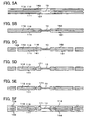
- Copper films are formed on both surfaces of the polyimide substrate 131 processed into a predetermined size. Next, the copper films are patterned to form the conductor layers 132 and 133 each having the wiring pattern 13a and the connection pads 13b.
- the insulating films 134 and 135 each including a polyimide layer are formed on the polyimide substrate 131 and the conductor layers 132 and 133, respectively. Furthermore, silver paste is applied except on the end of the flexible board 13, and the applied silver paste is cured to form the shield layers 136 and 137.
- the cover lays 138 and 139 are formed to cover the shield layers 136 and 137 on the front and the back surfaces, respectively.
- the flexible board 13 having the constitution shown in Fig. 4 is completed.
- the shield layers 136 and 137 and the cover lays 138 and 139 are formed avoiding the connection pads 13b.
- the first insulating film 111, the non-flexible substrate 112, and the second insulating layer 113, which constitute the core of the rigid board 11, are aligned.
- Each of the first and second insulating layers 111 and 113 includes, for example, a prepreg having a thickness of 20 to 50 ⁇ m
- the non-flexible substrate 112 includes, for example, a glass epoxy substrate having a thickness of about 100 ⁇ m.
- the thickness of the non-flexible substrate 112 is preferably substantially the same as the thickness of the flexible board 13.
- the space between the non-flexible substrate 112 and the cover lay 139 is filled with the resin 125, and thus the flexible board 13 and the non-flexible substrate 112 can be securely bonded together.
- the resin 125 filled in the space is cured integrally with the insulating layer 113 to fix the peripheries of the vias 116 with the resin 125, thereby improving the reliability of connection between the vias 116 and the conductor layer 133.
- the non-flexible substrate and the first and second insulating layers constituting the core portion of the rigid board 12 are aligned.
- one of the ends of the flexible board 13 is inserted between the first and second insulating layers 111 and 113 of the rigid board 11 and aligned, and the other end is disposed between the first and second insulating layers and the non-flexible substrate of the rigid board 12. Furthermore, conductor films 161 and 162 are disposed on and below these layers.
- the pressure pressing is performed, for example, using a bydropress apparatus at a temperature of 200°C and a pressure of 40 kgf for a pressure time of about 3 hours.
- the whole is heated to cure the prepreg constituting each of the first and second insulating layers 111 and 113 and the resin 125 to integrate the resins.
- the resin of the cover lays 138 and 139 of the flexible board 13 and the resin of the first and second insulating layers 111 and 113 are polymerized.
- the resin of the insulating layers 111 and 113 is polymerized to fix the peripheries of the vias 116 with the resin, thereby improving the reliability of connection between the vias 116 and the conductor layer 133.
- IVH Interstitial Via Hole 163 is formed by irradiation of CO 2 laser from a CO 2 laser processing apparatus according to demand.
- the vias 116 and 141 are formed for connecting the wiring layers 132 and 133 of the flexible board 13 to the rigid boards 11 and 12.
- Fig. 5D copper plating is conducted on the surfaces of the whole structure.
- the copper plating layers and the copper patterns 161 and 162 previously formed are integrated to form a copper film 171 over the entire surface of the board.
- the copper film 171 is formed in the vias 116 and 141.
- the flexible board 13 is covered with the copper foils 161 and 162 without making direct contact with a plating solution. Therefore, the flexible board 13 is not damaged by the plating solution.
- the copper film 171 on the surface of the board is patterned.
- the wiring patterns 117 and 142 connected to the conductor layers 132 and 133 of the flexible board 13 and the extraction patterns 118 and 143 are formed.
- the copper film 171 is left on the end portions of the first and second insulating layers 111 and 113.
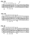
- each of the first and third upper insulating layers 114 and 144 includes, for example, a prepreg prepared by impregnating a glass cloth with a resin.
- the vias 116 and 141 are filled with the resin from the prepreg.
- the resin in the prepreg and the vias is cured by heating to fix the first and third upper insulating layers 114 and 144.
- the vias 119 and 144 are formed in the first and third upper insulating layers 114 and 144, respectively, and filled with a conductor by copper plating or the like.
- the vias 119 and 114 may be filled with conductive paste (e.g., thermosetting resin containing conductive particles) by printing such as screen printing and then subjected to resin curing.
- each of the second and fourth upper insulating layers 115 and 145 includes, for example, usual prepreg prepared by impregnating a glass cloth with a resin.
- the resin of the prepreg is cured by heating to fix the second and fourth upper insulating layers 115 and 145.
- the vias 121 and 147 are formed in the second and fourth upper insulating layers 115 and 145, respectively, and filled with a conductor by copper plating.
- the vias 121 and 147 may be filled with conductive paste (e.g., thermosetting resin containing conductive particles) by printing such as screen printing and then subjected to resin curing.
- conductive paste e.g., thermosetting resin containing conductive particles
- copper foil sheets with resin (resin copper film: RCF) 172 and 173 are disposed on the outermost layers of the board.
- vias 174 and 175 are formed in the RCFs 172 and 173, respectively.
- the vias 174 and 175 are filled with a conductor by copper plating. If required, the surface copper foils are patterned to form conductor patterns.
- the joint portions between the rigid boards 11 and 12 and the flexible board 13 are irradiated with laser beam 158, for example, CO 2 laser, from a laser processing apparatus, using as a stopper the copper foil 171 formed at the ends of the cores of rigid boards 11 and 12 to cut the upper insulating layers 114, 115, 144, and 145, and the copper foil sheets with resin (RCFs) 172 and 173.
- laser beam 158 for example, CO 2 laser
- the energy or irradiation time is controlled so as to cut the copper foil 171 used as a stopper to some extent.
- a structure 181 on the flexible board 13 is separated from the other portions.
- the structure 181 is removed from the flexible board 13 by peeling.
- the copper foils 161 and 162 (refer to Fig. 5B ), which are a base of the remaining copper foil 171, are only pressed by the cover lays 138 and 139 of the flexible board 13 and is not fixed. Similarly, the copper foil 171 is not fixed to the flexible board 13. Therefore, the copper foil 171 is also removed by removal of the structure 181.
- the copper foil 171 is removed from portions not covered with the other members. Therefore, the copper foils 124 and 151 are left on portions covered with the prepregs 113 and 144 at the ends of the first and second insulating layers 111 and 113.
- the flex-rigid wiring board 10 is completed, in which the ends of the flexible board 13 are held between the core portions (the first and second insulating layers 111 and 113) of the rigid boards 11 and 12, and the lands of the rigid boards 11 and 12 are connected to the connection pads of the flexible board by plating.
- RCF can be used on the outermost layers of the rigid boards 11 and 12. Therefore, the same reliability and dropping resistance as those of a usual rigid board can be secured.
- prepreg including a resin having a low flow property is required for forming the core layer of each of the rigid boards 11 and 13.
- usual prepreg can be used for layers other than the core layers, and thus IVH filling is not required, thereby little producing voids.
- a bending portion includes a flexible board, and thus stability is improved.
- holes are formed in a plurality of layers by laser processing after the formation of outer layers, and thus the manufacturing cost can be suppressed.
- the materials, sizes, and number of the layers may be appropriately changed.
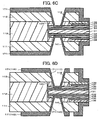
- the vias 116 and 141 may be filled with a conductor such as a plating metal.
- voids are present in the vias 116 and 141.
- the connection reliability of the vias may be degraded due to the expansion of the voids.
- the vias 116 and 141 are filled with a plating metal as shown in Fig. 7 , with the heat applied, the connection reliability of the vias 116 and 141 can be improved.
- conductor patterns (circuit patterns) 191 and 192 may be formed on the non-flexible substrate 112, for connection with any desired portion.
- conductor patterns (circuit patterns) 193 and 194 may be formed on the first and third upper insulating layers 114 and 144, for connection with any desired portion.
- the conductor patterns 191, 143, 193, and 150 are connected to each other through the vias 146 and 147 and any other vias.
- the conductor patterns 192, 118, 194, and 123 are connected to each other through the vias 119 and 121 and other vias.
- the conductor patterns 123 and 150 are connected to each other through the vias 163.
- the first and second insulating layers 111 and 113 which hold the end of the flexible board 13 therebetween may be composed of RCF.
- Each of the first and third upper insulating layers 114 and 144 and the second and fourth upper insulating layers 115 and 145 may be composed of RCF. In this constitution, a manufacturing step can be omitted.
- the flexible board 13 and the non-flexible substrate 112 have substantially the same thickness
- the present invention is not limited to this.
- the flexible board 13 may be thinner than the non-flexible substrate 112.
- the spaces between the flexible board 13, the non-flexible substrate 112, and the first and second insulating layers 111 and 113 are filled with any resin, for example, the resin seeping from the insulating layers 111 and 113 or a resin previously inserted for adjusting the height during manufacture. In this way, the spaces are filled with the resin 125, and thus the flexible board 13 and the non-flexible substrate 112 can be securely bonded together.
- the resin is integrally cured and fixed by heating during manufacture. Since the resins of the insulating layers 111 and 113 are polymerized, and the resin 125 is integrally cured and fixed, the peripheries of the vias 116 and 141 are fixed with the resin to improve the reliability of connection between the vias 116 and 141 and the conductor layers 133 and 132, respectively.
- the wiring patterns formed on the rigid boards 11 and 12 and the flexible board 13 are not limited to the example shown in Fig. 1 .
- the wiring patterns may be formed in a shape which fans out from the flexible board 13 toward the rigid boards 11 and 12.
- the pitch of wiring 13a of the flexible board 13 may be smaller than that on the connection portion 13b, in this case, many wirings can be disposed an the flexible hoard 13, and thus a flex-rigid wiring board having high-density wiring can be formed.
- an end of the flexible board 13 is widened to increase the area of a portion to be fixed to each of the rigid boards 11 and 12.
- the strength of the ends of the flexible board 13 can be increased to improve loading resistance.
- projections are formed at a position where bending of the flexible board 13 is repeated (for example, the position facing the end surfaces of the rigid boards 11 and 12) to increase the strength of the position where bending is repeated.
- the foregoing disclosure is applicable to a flexible rigid wiring board including a non-flexible substrate portion and a flexible substrate portion.
Landscapes
- Engineering & Computer Science (AREA)
- Microelectronics & Electronic Packaging (AREA)
- Manufacturing & Machinery (AREA)
- Production Of Multi-Layered Print Wiring Board (AREA)
- Printing Elements For Providing Electric Connections Between Printed Circuits (AREA)
- Structure Of Printed Boards (AREA)
Claims (9)
- Tableau de connexions flexible et rigide (10) comprenant :un substrat flexible (131) composé d'une feuille flexible isolante ;un tracé conducteur (132) formé sur le substrat flexible ;une couche de protection (139) couvrant le tracé conducteur ;un substrat non flexible (112) disposé adjacent au substrat flexible dans la direction horizontale ; etune couche isolante (113) couvrant le substrat flexible et le substrat non flexible pour exposer au moins une portion du substrat flexible ; etun tracé conducteur (117) formé sur la couche isolante ;caractérisé en ce que :le tracé conducteur (132) sur le substrat flexible est connecté par placage au tracé conducteur (117) sur la couche isolante par l'intermédiaire d'un trou d'interconnexion (116) formé dans la couche isolante dans une région dans laquelle la couche isolante couvre le substrat flexible ; etle substrat flexible est plus mince que le substrat non flexible.
- Tableau de connexions flexible et rigide selon la revendication 1,
dans lequel une deuxième couche isolante (135) est formée entre le tracé conducteur et la couche de protection,
le trou d'interconnexion est formé de manière à traverser la deuxième couche isolante,
la couche de protection est placée dans une région ne contenant pas le trou d'interconnexion, et
un espace entre le substrat non flexible et la couche de protection et dans la périphérie du trou d'interconnexion est rempli d'une résine (125). - Tableau de connexions flexible et rigide selon la revendication 1 ou la revendication 2,
dans lequel la couche de protection est placée dans une région ne contenant pas le trou d'interconnexion, et
l'épaisseur totale du substrat flexible, du tracé conducteur sur le substrat flexible et de la couche de protection est inférieure à celle du substrat non flexible, et
un espace entre la couche de protection et la couche isolante et dans la périphérie du trou d'interconnexion est rempli d'une résine,
la résine étant durcie d'une pièce avec la couche isolante. - Tableau de connexions flexible et rigide selon les revendications 1, 2 ou 3,
dans lequel l'épaisseur totale du substrat flexible, du tracé conducteur sur le substrat flexible et de la couche de protection est sensiblement égale à celle du substrat non flexible,
la couche de protection est placée dans une région ne contenant pas le trou d'interconnexion, et
un espace entre le substrat non flexible et la couche de protection et dans la périphérie du trou d'interconnexion est rempli d'une résine. - Tableau de connexions flexible et rigide selon les revendications 1, 2, 3 ou 4, dans lequel l'épaisseur totale du substrat flexible, du tracé conducteur sur le substrat flexible et de la couche de protection est sensiblement égale à celle du substrat non flexible,
la couche de protection est placée dans une région ne contenant pas le trou d'interconnexion, et
un espace entre le substrat non flexible et la couche de protection et dans la périphérie du trou d'interconnexion est rempli d'une résine,
la résine étant durcie d'une pièce avec la couche isolante. - Tableau de connexions flexible et rigide selon l'une des revendications 1 à 5, dans lequel les résines du substrat flexible et de la couche isolante sont polymérisées ensemble, la portion du tableau de connexions flexible et rigide sur laquelle ces couches sont polymérisées ensemble étant plus grande que des portions dans lesquelles les résines ne sont pas polymérisées de cette manière.
- Tableau de connexions flexible et rigide selon l'une des revendications 1 à 6, dans lequel dans le substrat flexible, la portion limite entre le substrat flexible et la couche isolante est plus grande que d'autres portions du tableau de connexions flexible et rigide.
- Tableau de connexions flexible et rigide selon l'une des revendications 1 à 7, dans lequel la couche de protection inclut un film isolant, et
un trou d'interconnexion est formé dans la couche isolante et le film isolant de manière à les traverser, pour une connexion électrique du tracé conducteur sur la couche isolante au tracé conducteur formé sur le substrat flexible. - Tableau de connexions flexible et rigide selon l'une des revendications 1 à 8, dans lequel la couche de protection du substrat flexible inclut une couche écran (137) protégeant contre une onde électromagnétique.
Applications Claiming Priority (2)
| Application Number | Priority Date | Filing Date | Title |
|---|---|---|---|
| PCT/JP2006/321160 WO2008050399A1 (fr) | 2006-10-24 | 2006-10-24 | Tableau de connexions rigide et flexible et son procédé de fabrication |
| EP06822140A EP2034810B1 (fr) | 2006-10-24 | 2006-10-24 | Tableau de connexions rigide et flexible |
Related Parent Applications (1)
| Application Number | Title | Priority Date | Filing Date |
|---|---|---|---|
| EP06822140.7 Division | 2006-10-24 |
Publications (2)
| Publication Number | Publication Date |
|---|---|
| EP2278866A1 EP2278866A1 (fr) | 2011-01-26 |
| EP2278866B1 true EP2278866B1 (fr) | 2012-05-09 |
Family
ID=38857845
Family Applications (6)
| Application Number | Title | Priority Date | Filing Date |
|---|---|---|---|
| EP10186158A Not-in-force EP2278866B1 (fr) | 2006-10-24 | 2006-10-24 | Tableau de connexions rigide et flexible |
| EP11189512A Withdrawn EP2432305A1 (fr) | 2006-10-24 | 2006-10-24 | Carte de circuit flexible-rigide et procédé de fabrication correspondant |
| EP10186155A Not-in-force EP2268112B1 (fr) | 2006-10-24 | 2006-10-24 | Procédé de fabrication d'un tableau de connexions rigide et flexible |
| EP11189511A Withdrawn EP2434848A1 (fr) | 2006-10-24 | 2006-10-24 | Carte de circuit flexible-rigide et procédé de fabrication correspondant |
| EP10186163A Withdrawn EP2268113A1 (fr) | 2006-10-24 | 2006-10-24 | Tableau de connexions rigide et flexible et son procédé de fabrication |
| EP06822140A Not-in-force EP2034810B1 (fr) | 2006-10-24 | 2006-10-24 | Tableau de connexions rigide et flexible |
Family Applications After (5)
| Application Number | Title | Priority Date | Filing Date |
|---|---|---|---|
| EP11189512A Withdrawn EP2432305A1 (fr) | 2006-10-24 | 2006-10-24 | Carte de circuit flexible-rigide et procédé de fabrication correspondant |
| EP10186155A Not-in-force EP2268112B1 (fr) | 2006-10-24 | 2006-10-24 | Procédé de fabrication d'un tableau de connexions rigide et flexible |
| EP11189511A Withdrawn EP2434848A1 (fr) | 2006-10-24 | 2006-10-24 | Carte de circuit flexible-rigide et procédé de fabrication correspondant |
| EP10186163A Withdrawn EP2268113A1 (fr) | 2006-10-24 | 2006-10-24 | Tableau de connexions rigide et flexible et son procédé de fabrication |
| EP06822140A Not-in-force EP2034810B1 (fr) | 2006-10-24 | 2006-10-24 | Tableau de connexions rigide et flexible |
Country Status (7)
| Country | Link |
|---|---|
| EP (6) | EP2278866B1 (fr) |
| JP (1) | JP4021472B1 (fr) |
| KR (1) | KR100939426B1 (fr) |
| CN (1) | CN100559920C (fr) |
| AT (1) | ATE557577T1 (fr) |
| TW (1) | TWI304318B (fr) |
| WO (1) | WO2008050399A1 (fr) |
Cited By (1)
| Publication number | Priority date | Publication date | Assignee | Title |
|---|---|---|---|---|
| DE102016217563A1 (de) | 2016-09-14 | 2018-03-15 | Feinmetall Gmbh | Kontaktstift, insbesondere Federkontaktstift |
Families Citing this family (35)
| Publication number | Priority date | Publication date | Assignee | Title |
|---|---|---|---|---|
| US8071883B2 (en) | 2006-10-23 | 2011-12-06 | Ibiden Co., Ltd. | Flex-rigid wiring board including flexible substrate and non-flexible substrate and method of manufacturing the same |
| US7982135B2 (en) | 2006-10-30 | 2011-07-19 | Ibiden Co., Ltd. | Flex-rigid wiring board and method of manufacturing the same |
| KR101098072B1 (ko) | 2008-03-10 | 2011-12-26 | 이비덴 가부시키가이샤 | 가요성 배선판 및 그의 제조 방법 |
| WO2009118935A1 (fr) * | 2008-03-26 | 2009-10-01 | イビデン株式会社 | Plaquette de circuits imprimés flexo-rigide, et procédé de fabrication associé |
| EP2280594A4 (fr) | 2008-05-19 | 2012-06-27 | Ibiden Co Ltd | Carte à circuits imprimés et procédé de fabrication correspondant |
| KR101208379B1 (ko) * | 2008-05-19 | 2012-12-05 | 이비덴 가부시키가이샤 | 배선판과 그 제조 방법 |
| WO2010007704A1 (fr) * | 2008-07-16 | 2010-01-21 | イビデン株式会社 | Carte de câblage flexorigide et dispositif électronique |
| WO2010013366A1 (fr) | 2008-07-30 | 2010-02-04 | イビデン株式会社 | Carte de câblage flexorigide et son procédé de fabrication |
| KR20100095033A (ko) * | 2008-08-29 | 2010-08-27 | 이비덴 가부시키가이샤 | 플렉스 리지드 배선판 및 전자 디바이스 |
| US20100155109A1 (en) | 2008-12-24 | 2010-06-24 | Ibiden Co., Ltd. | Flex-rigid wiring board and method for manufacturing the same |
| US8383948B2 (en) | 2009-09-18 | 2013-02-26 | Ibiden Co., Ltd. | Flex-rigid wiring board and method for manufacturing the same |
| KR101051491B1 (ko) | 2009-10-28 | 2011-07-22 | 삼성전기주식회사 | 다층 경연성 인쇄회로기판 및 다층 경연성 인쇄회로기판의 제조방법 |
| US8334463B2 (en) * | 2009-10-30 | 2012-12-18 | Ibiden Co., Ltd. | Wiring board and method for manufacturing the same |
| TW201127228A (en) | 2010-01-22 | 2011-08-01 | Ibiden Co Ltd | Flex-rigid wiring board and method for manufacturing the same |
| TW201127246A (en) | 2010-01-22 | 2011-08-01 | Ibiden Co Ltd | Flex-rigid wiring board and method for manufacturing the same |
| US8493747B2 (en) | 2010-02-05 | 2013-07-23 | Ibiden Co., Ltd. | Flex-rigid wiring board and method for manufacturing the same |
| US8404978B2 (en) * | 2010-02-12 | 2013-03-26 | Ibiden Co., Ltd. | Flex-rigid wiring board and method for manufacturing the same |
| US8759687B2 (en) | 2010-02-12 | 2014-06-24 | Ibiden Co., Ltd. | Flex-rigid wiring board and method for manufacturing the same |
| US8519270B2 (en) | 2010-05-19 | 2013-08-27 | Unimicron Technology Corp. | Circuit board and manufacturing method thereof |
| CN102378489B (zh) * | 2010-08-24 | 2013-11-20 | 欣兴电子股份有限公司 | 软硬线路板的制造方法 |
| TWI405524B (zh) * | 2010-11-24 | 2013-08-11 | Unimicron Technology Corp | 線路板及其製作方法 |
| TW201233264A (en) * | 2011-01-20 | 2012-08-01 | Unitech Printed Circuit Board Corp | Method for manufacturing flexible and hard composite printed circuit board |
| JP2012234937A (ja) * | 2011-04-28 | 2012-11-29 | Nec Toppan Circuit Solutions Inc | リジッドフレキシブルプリント配線板及びその製造方法 |
| EP2547183A1 (fr) | 2011-07-15 | 2013-01-16 | AT & S Austria Technologie & Systemtechnik Aktiengesellschaft | Procédé de fabrication d'un circuit imprimé flex-rigide ou un sous-ensemble de celui-ci ainsi que circuit imprimé flex-rigide ou un sous-ensemble de celui-ci |
| EP2547182A1 (fr) | 2011-07-15 | 2013-01-16 | AT & S Austria Technologie & Systemtechnik Aktiengesellschaft | Procédé de fabrication d'un circuit imprimé ou un sous-ensemble de celui-ci ainsi que circuit imprimé ou un sous-ensemble de celui-ci et leur utilisation |
| CN103179789A (zh) * | 2011-12-22 | 2013-06-26 | 深圳市大族激光科技股份有限公司 | 一种软硬结合板的开盖方法及其操作系统 |
| JP2015082645A (ja) | 2013-10-24 | 2015-04-27 | イビデン株式会社 | フレックスリジッド配線板及びフレックスリジッド配線板の製造方法 |
| CN105578739A (zh) * | 2016-02-25 | 2016-05-11 | 广东欧珀移动通信有限公司 | 电路板及终端 |
| CN106793494A (zh) * | 2017-03-02 | 2017-05-31 | 东莞市五株电子科技有限公司 | 软硬结合印刷电路板及其制作方法 |
| CN109757022A (zh) * | 2017-11-01 | 2019-05-14 | 健鼎(无锡)电子有限公司 | 软硬复合电路板及其制造方法 |
| US10847908B2 (en) * | 2018-07-25 | 2020-11-24 | Sharp Kabushiki Kaisha | Connected board and display device |
| US10638616B1 (en) | 2018-10-30 | 2020-04-28 | Taiwan Semiconductor Manufacturing Co., Ltd. | Circuit carrier and manifacturing method thereof |
| CN112752440B (zh) * | 2019-10-29 | 2022-10-18 | 庆鼎精密电子(淮安)有限公司 | 软硬结合线路板及其制作方法 |
| CA3194224A1 (fr) * | 2020-10-06 | 2022-04-14 | Francis Zaato | Techniques destinees a fabriquer et a separer des dispositifs microelectroniques flexibles de substrats rigides |
| CN112672523A (zh) * | 2021-01-31 | 2021-04-16 | 惠州中京电子科技有限公司 | 一种薄铜细线单面软板的制作方法 |
Family Cites Families (18)
| Publication number | Priority date | Publication date | Assignee | Title |
|---|---|---|---|---|
| US4715928A (en) * | 1985-09-27 | 1987-12-29 | Hamby Bill L | Flexible printed circuits and methods of fabricating and forming plated thru-holes therein |
| JPS63293991A (ja) * | 1987-05-19 | 1988-11-30 | ビル エル.ハムビ− | フレキシブルプリント回路およびその製造方法 |
| JPH0590756A (ja) * | 1991-09-28 | 1993-04-09 | Ibiden Co Ltd | リジツドフレキ基板の製造方法 |
| GB9125173D0 (en) * | 1991-11-27 | 1992-01-29 | Northumbria Circuits Limited | Printed circuit combination and process |
| DE4208610C1 (en) * | 1992-03-18 | 1993-05-19 | Fa. Carl Freudenberg, 6940 Weinheim, De | Rigid-flexible PCB with flexible circuit foil mfg. - having flexible PCB in flexible region with fracture lines in rigid outer layers along rigid-flexible transition allowing rigid part to be removed along fracture lines after processing |
| JPH05315758A (ja) * | 1992-05-01 | 1993-11-26 | Nitto Denko Corp | 多層フレキシブル回路基板およびその製法 |
| JPH0794835A (ja) * | 1993-09-21 | 1995-04-07 | Nippon Avionics Co Ltd | フレキシブル・リジッド・プリント配線板 |
| US6350387B2 (en) * | 1997-02-14 | 2002-02-26 | Teledyne Industries, Inc. | Multilayer combined rigid/flex printed circuit board containing flexible soldermask |
| US6099745A (en) * | 1998-06-05 | 2000-08-08 | Parlex Corporation | Rigid/flex printed circuit board and manufacturing method therefor |
| JP2003332743A (ja) * | 2002-05-14 | 2003-11-21 | Olympus Optical Co Ltd | リジットフレキシブル基板 |
| JP3906225B2 (ja) * | 2002-11-27 | 2007-04-18 | 住友ベークライト株式会社 | 回路基板、多層配線板、回路基板の製造方法および多層配線板の製造方法 |
| FR2854023B1 (fr) | 2003-04-16 | 2007-04-13 | Valeo Systemes Dessuyage | Boitier comportant un conduit de circulation d'air empechant toute accumulation de liquide |
| CN1765161B (zh) | 2003-04-18 | 2011-06-22 | 揖斐电株式会社 | 刚挠性电路板 |
| JP4408343B2 (ja) * | 2003-04-30 | 2010-02-03 | 日本圧着端子製造株式会社 | 多層プリント配線板の接続構造 |
| JP4574311B2 (ja) * | 2004-09-30 | 2010-11-04 | 大日本印刷株式会社 | リジッド−フレキシブル基板の製造方法 |
| JP4574310B2 (ja) | 2004-09-30 | 2010-11-04 | 大日本印刷株式会社 | リジッド−フレキシブル基板の製造方法 |
| JP2006140213A (ja) | 2004-11-10 | 2006-06-01 | Cmk Corp | リジッドフレックス多層プリント配線板 |
| JP2006196800A (ja) * | 2005-01-17 | 2006-07-27 | Cmk Corp | リジッドフレックス多層プリント配線板及びその製造方法 |
-
2006
- 2006-10-24 EP EP10186158A patent/EP2278866B1/fr not_active Not-in-force
- 2006-10-24 WO PCT/JP2006/321160 patent/WO2008050399A1/fr active Application Filing
- 2006-10-24 EP EP11189512A patent/EP2432305A1/fr not_active Withdrawn
- 2006-10-24 EP EP10186155A patent/EP2268112B1/fr not_active Not-in-force
- 2006-10-24 KR KR1020097002440A patent/KR100939426B1/ko not_active IP Right Cessation
- 2006-10-24 AT AT10186158T patent/ATE557577T1/de active
- 2006-10-24 CN CNB2006800349321A patent/CN100559920C/zh not_active Expired - Fee Related
- 2006-10-24 EP EP11189511A patent/EP2434848A1/fr not_active Withdrawn
- 2006-10-24 EP EP10186163A patent/EP2268113A1/fr not_active Withdrawn
- 2006-10-24 JP JP2007513540A patent/JP4021472B1/ja not_active Expired - Fee Related
- 2006-10-24 EP EP06822140A patent/EP2034810B1/fr not_active Not-in-force
-
2007
- 2007-04-27 TW TW096115148A patent/TWI304318B/zh not_active IP Right Cessation
Cited By (2)
| Publication number | Priority date | Publication date | Assignee | Title |
|---|---|---|---|---|
| DE102016217563A1 (de) | 2016-09-14 | 2018-03-15 | Feinmetall Gmbh | Kontaktstift, insbesondere Federkontaktstift |
| US11360119B2 (en) | 2016-09-14 | 2022-06-14 | Feinmetall Gmbh | Contact pin, in particular spring contact pin |
Also Published As
| Publication number | Publication date |
|---|---|
| EP2034810A4 (fr) | 2010-04-28 |
| EP2268113A1 (fr) | 2010-12-29 |
| EP2034810A1 (fr) | 2009-03-11 |
| ATE557577T1 (de) | 2012-05-15 |
| EP2034810B1 (fr) | 2011-12-14 |
| EP2278866A1 (fr) | 2011-01-26 |
| CN101310574A (zh) | 2008-11-19 |
| WO2008050399A1 (fr) | 2008-05-02 |
| TWI304318B (en) | 2008-12-11 |
| KR20090017705A (ko) | 2009-02-18 |
| CN100559920C (zh) | 2009-11-11 |
| EP2268112B1 (fr) | 2012-08-22 |
| TW200820866A (en) | 2008-05-01 |
| EP2268112A1 (fr) | 2010-12-29 |
| EP2432305A1 (fr) | 2012-03-21 |
| JPWO2008050399A1 (ja) | 2010-02-25 |
| JP4021472B1 (ja) | 2007-12-12 |
| EP2434848A1 (fr) | 2012-03-28 |
| KR100939426B1 (ko) | 2010-01-28 |
Similar Documents
| Publication | Publication Date | Title |
|---|---|---|
| EP2278866B1 (fr) | Tableau de connexions rigide et flexible | |
| US8476531B2 (en) | Flex-rigid wiring board and method of manufacturing the same | |
| JP4024846B1 (ja) | フレックスリジッド配線板及びその製造方法 | |
| US8525038B2 (en) | Flex-rigid wiring board and method of manufacturing the same | |
| JP4971460B2 (ja) | フレキシブル配線板及びその製造方法 | |
| US8493747B2 (en) | Flex-rigid wiring board and method for manufacturing the same | |
| US8399775B2 (en) | Flex-rigid wiring board and method of manufacturing the same | |
| KR100942626B1 (ko) | 플렉스 리지드 배선판 및 그 제조 방법 | |
| JPH1056267A (ja) | 多層プリント配線板及びその製造方法 |
Legal Events
| Date | Code | Title | Description |
|---|---|---|---|
| PUAI | Public reference made under article 153(3) epc to a published international application that has entered the european phase |
Free format text: ORIGINAL CODE: 0009012 |
|
| 17P | Request for examination filed |
Effective date: 20101210 |
|
| AC | Divisional application: reference to earlier application |
Ref document number: 2034810 Country of ref document: EP Kind code of ref document: P |
|
| AK | Designated contracting states |
Kind code of ref document: A1 Designated state(s): AT BE BG CH CY CZ DE DK EE ES FI FR GB GR HU IE IS IT LI LT LU LV MC NL PL PT RO SE SI SK TR |
|
| RTI1 | Title (correction) |
Free format text: FLEX-RIGID WIRING BOARD |
|
| GRAP | Despatch of communication of intention to grant a patent |
Free format text: ORIGINAL CODE: EPIDOSNIGR1 |
|
| GRAS | Grant fee paid |
Free format text: ORIGINAL CODE: EPIDOSNIGR3 |
|
| GRAA | (expected) grant |
Free format text: ORIGINAL CODE: 0009210 |
|
| RAP1 | Party data changed (applicant data changed or rights of an application transferred) |
Owner name: IBIDEN CO., LTD. |
|
| AC | Divisional application: reference to earlier application |
Ref document number: 2034810 Country of ref document: EP Kind code of ref document: P |
|
| AK | Designated contracting states |
Kind code of ref document: B1 Designated state(s): AT BE BG CH CY CZ DE DK EE ES FI FR GB GR HU IE IS IT LI LT LU LV MC NL PL PT RO SE SI SK TR |
|
| REG | Reference to a national code |
Ref country code: GB Ref legal event code: FG4D |
|
| REG | Reference to a national code |
Ref country code: AT Ref legal event code: REF Ref document number: 557577 Country of ref document: AT Kind code of ref document: T Effective date: 20120515 Ref country code: CH Ref legal event code: EP |
|
| REG | Reference to a national code |
Ref country code: IE Ref legal event code: FG4D |
|
| REG | Reference to a national code |
Ref country code: DE Ref legal event code: R096 Ref document number: 602006029366 Country of ref document: DE Effective date: 20120705 |
|
| REG | Reference to a national code |
Ref country code: NL Ref legal event code: VDEP Effective date: 20120509 |
|
| REG | Reference to a national code |
Ref country code: LT Ref legal event code: MG4D Effective date: 20120509 |
|
| PG25 | Lapsed in a contracting state [announced via postgrant information from national office to epo] |
Ref country code: SE Free format text: LAPSE BECAUSE OF FAILURE TO SUBMIT A TRANSLATION OF THE DESCRIPTION OR TO PAY THE FEE WITHIN THE PRESCRIBED TIME-LIMIT Effective date: 20120509 Ref country code: IS Free format text: LAPSE BECAUSE OF FAILURE TO SUBMIT A TRANSLATION OF THE DESCRIPTION OR TO PAY THE FEE WITHIN THE PRESCRIBED TIME-LIMIT Effective date: 20120909 Ref country code: FI Free format text: LAPSE BECAUSE OF FAILURE TO SUBMIT A TRANSLATION OF THE DESCRIPTION OR TO PAY THE FEE WITHIN THE PRESCRIBED TIME-LIMIT Effective date: 20120509 Ref country code: PL Free format text: LAPSE BECAUSE OF FAILURE TO SUBMIT A TRANSLATION OF THE DESCRIPTION OR TO PAY THE FEE WITHIN THE PRESCRIBED TIME-LIMIT Effective date: 20120509 Ref country code: LT Free format text: LAPSE BECAUSE OF FAILURE TO SUBMIT A TRANSLATION OF THE DESCRIPTION OR TO PAY THE FEE WITHIN THE PRESCRIBED TIME-LIMIT Effective date: 20120509 Ref country code: CY Free format text: LAPSE BECAUSE OF FAILURE TO SUBMIT A TRANSLATION OF THE DESCRIPTION OR TO PAY THE FEE WITHIN THE PRESCRIBED TIME-LIMIT Effective date: 20120509 |
|
| REG | Reference to a national code |
Ref country code: AT Ref legal event code: MK05 Ref document number: 557577 Country of ref document: AT Kind code of ref document: T Effective date: 20120509 |
|
| PG25 | Lapsed in a contracting state [announced via postgrant information from national office to epo] |
Ref country code: LV Free format text: LAPSE BECAUSE OF FAILURE TO SUBMIT A TRANSLATION OF THE DESCRIPTION OR TO PAY THE FEE WITHIN THE PRESCRIBED TIME-LIMIT Effective date: 20120509 Ref country code: PT Free format text: LAPSE BECAUSE OF FAILURE TO SUBMIT A TRANSLATION OF THE DESCRIPTION OR TO PAY THE FEE WITHIN THE PRESCRIBED TIME-LIMIT Effective date: 20120910 Ref country code: GR Free format text: LAPSE BECAUSE OF FAILURE TO SUBMIT A TRANSLATION OF THE DESCRIPTION OR TO PAY THE FEE WITHIN THE PRESCRIBED TIME-LIMIT Effective date: 20120810 Ref country code: SI Free format text: LAPSE BECAUSE OF FAILURE TO SUBMIT A TRANSLATION OF THE DESCRIPTION OR TO PAY THE FEE WITHIN THE PRESCRIBED TIME-LIMIT Effective date: 20120509 |
|
| PG25 | Lapsed in a contracting state [announced via postgrant information from national office to epo] |
Ref country code: BE Free format text: LAPSE BECAUSE OF FAILURE TO SUBMIT A TRANSLATION OF THE DESCRIPTION OR TO PAY THE FEE WITHIN THE PRESCRIBED TIME-LIMIT Effective date: 20120509 |
|
| PG25 | Lapsed in a contracting state [announced via postgrant information from national office to epo] |
Ref country code: CZ Free format text: LAPSE BECAUSE OF FAILURE TO SUBMIT A TRANSLATION OF THE DESCRIPTION OR TO PAY THE FEE WITHIN THE PRESCRIBED TIME-LIMIT Effective date: 20120509 Ref country code: EE Free format text: LAPSE BECAUSE OF FAILURE TO SUBMIT A TRANSLATION OF THE DESCRIPTION OR TO PAY THE FEE WITHIN THE PRESCRIBED TIME-LIMIT Effective date: 20120509 Ref country code: AT Free format text: LAPSE BECAUSE OF FAILURE TO SUBMIT A TRANSLATION OF THE DESCRIPTION OR TO PAY THE FEE WITHIN THE PRESCRIBED TIME-LIMIT Effective date: 20120509 Ref country code: DK Free format text: LAPSE BECAUSE OF FAILURE TO SUBMIT A TRANSLATION OF THE DESCRIPTION OR TO PAY THE FEE WITHIN THE PRESCRIBED TIME-LIMIT Effective date: 20120509 Ref country code: SK Free format text: LAPSE BECAUSE OF FAILURE TO SUBMIT A TRANSLATION OF THE DESCRIPTION OR TO PAY THE FEE WITHIN THE PRESCRIBED TIME-LIMIT Effective date: 20120509 Ref country code: NL Free format text: LAPSE BECAUSE OF FAILURE TO SUBMIT A TRANSLATION OF THE DESCRIPTION OR TO PAY THE FEE WITHIN THE PRESCRIBED TIME-LIMIT Effective date: 20120509 Ref country code: RO Free format text: LAPSE BECAUSE OF FAILURE TO SUBMIT A TRANSLATION OF THE DESCRIPTION OR TO PAY THE FEE WITHIN THE PRESCRIBED TIME-LIMIT Effective date: 20120509 |
|
| PG25 | Lapsed in a contracting state [announced via postgrant information from national office to epo] |
Ref country code: IT Free format text: LAPSE BECAUSE OF FAILURE TO SUBMIT A TRANSLATION OF THE DESCRIPTION OR TO PAY THE FEE WITHIN THE PRESCRIBED TIME-LIMIT Effective date: 20120509 |
|
| PLBE | No opposition filed within time limit |
Free format text: ORIGINAL CODE: 0009261 |
|
| STAA | Information on the status of an ep patent application or granted ep patent |
Free format text: STATUS: NO OPPOSITION FILED WITHIN TIME LIMIT |
|
| 26N | No opposition filed |
Effective date: 20130212 |
|
| PG25 | Lapsed in a contracting state [announced via postgrant information from national office to epo] |
Ref country code: ES Free format text: LAPSE BECAUSE OF FAILURE TO SUBMIT A TRANSLATION OF THE DESCRIPTION OR TO PAY THE FEE WITHIN THE PRESCRIBED TIME-LIMIT Effective date: 20120820 |
|
| PG25 | Lapsed in a contracting state [announced via postgrant information from national office to epo] |
Ref country code: MC Free format text: LAPSE BECAUSE OF NON-PAYMENT OF DUE FEES Effective date: 20121031 |
|
| REG | Reference to a national code |
Ref country code: CH Ref legal event code: PL |
|
| REG | Reference to a national code |
Ref country code: DE Ref legal event code: R097 Ref document number: 602006029366 Country of ref document: DE Effective date: 20130212 |
|
| GBPC | Gb: european patent ceased through non-payment of renewal fee |
Effective date: 20121024 |
|
| REG | Reference to a national code |
Ref country code: IE Ref legal event code: MM4A |
|
| REG | Reference to a national code |
Ref country code: FR Ref legal event code: ST Effective date: 20130628 |
|
| PG25 | Lapsed in a contracting state [announced via postgrant information from national office to epo] |
Ref country code: LI Free format text: LAPSE BECAUSE OF NON-PAYMENT OF DUE FEES Effective date: 20121031 Ref country code: BG Free format text: LAPSE BECAUSE OF FAILURE TO SUBMIT A TRANSLATION OF THE DESCRIPTION OR TO PAY THE FEE WITHIN THE PRESCRIBED TIME-LIMIT Effective date: 20120809 Ref country code: IE Free format text: LAPSE BECAUSE OF NON-PAYMENT OF DUE FEES Effective date: 20121024 Ref country code: GB Free format text: LAPSE BECAUSE OF NON-PAYMENT OF DUE FEES Effective date: 20121024 Ref country code: CH Free format text: LAPSE BECAUSE OF NON-PAYMENT OF DUE FEES Effective date: 20121031 |
|
| PG25 | Lapsed in a contracting state [announced via postgrant information from national office to epo] |
Ref country code: FR Free format text: LAPSE BECAUSE OF NON-PAYMENT OF DUE FEES Effective date: 20121031 |
|
| PG25 | Lapsed in a contracting state [announced via postgrant information from national office to epo] |
Ref country code: TR Free format text: LAPSE BECAUSE OF FAILURE TO SUBMIT A TRANSLATION OF THE DESCRIPTION OR TO PAY THE FEE WITHIN THE PRESCRIBED TIME-LIMIT Effective date: 20120509 |
|
| PG25 | Lapsed in a contracting state [announced via postgrant information from national office to epo] |
Ref country code: LU Free format text: LAPSE BECAUSE OF NON-PAYMENT OF DUE FEES Effective date: 20121024 |
|
| PG25 | Lapsed in a contracting state [announced via postgrant information from national office to epo] |
Ref country code: HU Free format text: LAPSE BECAUSE OF FAILURE TO SUBMIT A TRANSLATION OF THE DESCRIPTION OR TO PAY THE FEE WITHIN THE PRESCRIBED TIME-LIMIT Effective date: 20061024 |
|
| PGFP | Annual fee paid to national office [announced via postgrant information from national office to epo] |
Ref country code: DE Payment date: 20181009 Year of fee payment: 13 |
|
| REG | Reference to a national code |
Ref country code: DE Ref legal event code: R119 Ref document number: 602006029366 Country of ref document: DE |
|
| PG25 | Lapsed in a contracting state [announced via postgrant information from national office to epo] |
Ref country code: DE Free format text: LAPSE BECAUSE OF NON-PAYMENT OF DUE FEES Effective date: 20200501 |