EP2273551A1 - Röhrenlose abbildungseinrichtung - Google Patents
Röhrenlose abbildungseinrichtung Download PDFInfo
- Publication number
- EP2273551A1 EP2273551A1 EP09724745A EP09724745A EP2273551A1 EP 2273551 A1 EP2273551 A1 EP 2273551A1 EP 09724745 A EP09724745 A EP 09724745A EP 09724745 A EP09724745 A EP 09724745A EP 2273551 A1 EP2273551 A1 EP 2273551A1
- Authority
- EP
- European Patent Office
- Prior art keywords
- charge
- potential
- transferring
- accumulated
- portions
- Prior art date
- Legal status (The legal status is an assumption and is not a legal conclusion. Google has not performed a legal analysis and makes no representation as to the accuracy of the status listed.)
- Granted
Links
- 238000003384 imaging method Methods 0.000 title claims abstract description 29
- 239000004065 semiconductor Substances 0.000 description 82
- 238000002955 isolation Methods 0.000 description 14
- 238000010586 diagram Methods 0.000 description 7
- 239000012535 impurity Substances 0.000 description 6
- 238000013508 migration Methods 0.000 description 5
- 230000005012 migration Effects 0.000 description 5
- 229910021420 polycrystalline silicon Inorganic materials 0.000 description 5
- 229920005591 polysilicon Polymers 0.000 description 5
- 229920006395 saturated elastomer Polymers 0.000 description 5
- 238000001514 detection method Methods 0.000 description 4
- 239000000758 substrate Substances 0.000 description 4
- 238000007599 discharging Methods 0.000 description 3
- 238000009792 diffusion process Methods 0.000 description 2
- 239000012780 transparent material Substances 0.000 description 2
- ZOXJGFHDIHLPTG-UHFFFAOYSA-N Boron Chemical compound [B] ZOXJGFHDIHLPTG-UHFFFAOYSA-N 0.000 description 1
- VYPSYNLAJGMNEJ-UHFFFAOYSA-N Silicium dioxide Chemical compound O=[Si]=O VYPSYNLAJGMNEJ-UHFFFAOYSA-N 0.000 description 1
- 239000000370 acceptor Substances 0.000 description 1
- 238000009825 accumulation Methods 0.000 description 1
- 229910052785 arsenic Inorganic materials 0.000 description 1
- RQNWIZPPADIBDY-UHFFFAOYSA-N arsenic atom Chemical compound [As] RQNWIZPPADIBDY-UHFFFAOYSA-N 0.000 description 1
- 229910052796 boron Inorganic materials 0.000 description 1
- 230000007423 decrease Effects 0.000 description 1
- 230000000694 effects Effects 0.000 description 1
- 229910052814 silicon oxide Inorganic materials 0.000 description 1
Images


Classifications
-
- H—ELECTRICITY
- H01—ELECTRIC ELEMENTS
- H01L—SEMICONDUCTOR DEVICES NOT COVERED BY CLASS H10
- H01L27/00—Devices consisting of a plurality of semiconductor or other solid-state components formed in or on a common substrate
- H01L27/14—Devices consisting of a plurality of semiconductor or other solid-state components formed in or on a common substrate including semiconductor components sensitive to infrared radiation, light, electromagnetic radiation of shorter wavelength or corpuscular radiation and specially adapted either for the conversion of the energy of such radiation into electrical energy or for the control of electrical energy by such radiation
- H01L27/144—Devices controlled by radiation
- H01L27/146—Imager structures
- H01L27/148—Charge coupled imagers
- H01L27/14825—Linear CCD imagers
-
- H—ELECTRICITY
- H04—ELECTRIC COMMUNICATION TECHNIQUE
- H04N—PICTORIAL COMMUNICATION, e.g. TELEVISION
- H04N25/00—Circuitry of solid-state image sensors [SSIS]; Control thereof
- H04N25/70—SSIS architectures; Circuits associated therewith
- H04N25/701—Line sensors
-
- H—ELECTRICITY
- H04—ELECTRIC COMMUNICATION TECHNIQUE
- H04N—PICTORIAL COMMUNICATION, e.g. TELEVISION
- H04N25/00—Circuitry of solid-state image sensors [SSIS]; Control thereof
- H04N25/50—Control of the SSIS exposure
- H04N25/53—Control of the integration time
- H04N25/533—Control of the integration time by using differing integration times for different sensor regions
-
- G—PHYSICS
- G01—MEASURING; TESTING
- G01J—MEASUREMENT OF INTENSITY, VELOCITY, SPECTRAL CONTENT, POLARISATION, PHASE OR PULSE CHARACTERISTICS OF INFRARED, VISIBLE OR ULTRAVIOLET LIGHT; COLORIMETRY; RADIATION PYROMETRY
- G01J3/00—Spectrometry; Spectrophotometry; Monochromators; Measuring colours
- G01J3/28—Investigating the spectrum
- G01J3/2803—Investigating the spectrum using photoelectric array detector
Definitions
- the present invention relates to a solid-state imaging device.
- the solid-state imaging device described in Patent Document 1 has the following problem.
- a charge generated in the photosensitive region is read out from the short side of the photosensitive region.
- the generated charge needs to migrate in the long side direction of the photosensitive region and a migration distance thereof is long. As a result of this, it becomes difficult to quickly read out the generated charge.
- a diffusion region for accumulation of charge and an amplifier region for amplifying and outputting a voltage signal generated in the diffusion region are arranged adjacent to each of a pair of short sides of the photosensitive region. Namely, since the solid-state imaging device described in Patent Document 1 is configured to output respective signals from a pair of amplifier regions arranged adjacent to the respective short sides of the photosensitive region, it is necessary to execute signal processing for obtaining a one-dimensional image. As a result of this, it could complicate image processing.
- An object of the present invention is to provide a solid-state imaging device capable of quickly reading out the charge generated in the photosensitive region, without complicating image processing.
- a solid-state imaging device comprises: a plurality of photoelectric converting portions, each having a photosensitive region which generates a charge according to incidence of light and which has a planar shape of a nearly rectangular shape composed of two long sides and two short sides, and a potential gradient forming region which forms a potential gradient increasing along a first direction directed from one short side to the other short side forming the planar shape of the photosensitive region, in the photosensitive region, the plurality of photoelectric converting portions being juxtaposed along a second direction intersecting with the first direction; a plurality of first transferring portions arranged corresponding to the respective photoelectric converting portions and on the side of the other short side forming the planar shape of the photosensitive region, each first transferring portion transferring a charge acquired from the corresponding photoelectric converting portion, in the first direction; a plurality of charge accumulating portions arranged corresponding to the respective first transferring portions, each charge accumulating portion accumulating a charge transferred from the corresponding first transferring portion; a plurality
- the charge generated in the photosensitive region migrates toward the other short side along a slope of potential according to the potential gradient thus formed.
- the charge having migrated to the other short side is acquired by the first transferring portion to be transferred in the first direction. This makes the charge migration speed dominated by the potential gradient (slope of potential), so as to increase the charge readout speed.
- the charge transferred from the first transferring portion is accumulated in the charge accumulating portion and thereafter the charge is transferred in the first direction by the second transferring portion. Then the charges transferred from the respective second transferring portions are transferred in the second direction and output by the charge output portion.
- the present invention does not have to execute further signal processing for obtaining a one-dimensional image, whereby image processing can be prevented from becoming complicated.
- the photosensitive region has the planar shape of the nearly rectangular shape composed of two long sides and two shorts sides. For this reason, a saturated charge quantity is large in the photosensitive region.
- a charge generated in the photoelectric converting portion during a first period and a charge generated in the photoelectric converting portion during a second period shorter than the first period are continuously and alternately output.
- an exposure time is relatively long and therefore strong incident light causes saturation of a signal and makes appropriate detection thereof difficult; weak incident light is detected as a sufficiently large signal.
- an exposure time is relatively short and therefore weak incident light leads to a very weak signal and makes sufficient signal detection difficult; strong incident light is appropriately detected as a signal, without saturation. In this manner, the incident light is appropriately detected as a signal, regardless of the intensity of incident light, so as to increase the effective dynamic range.
- the present invention comprises the charge accumulating portions. This permits the charge generated in the photoelectric converting portion during the first period to be accumulated and transferred through the second transferring portion to the charge output portion so as to pose no impediment in transferring the charge generated in the photoelectric converting portion during the second period.
- the present invention successfully provides the solid-state imaging device capable of quickly reading out the charge generated in the photosensitive region, without complicating image processing.
- FIG. 1 is a drawing showing a configuration of a solid-state imaging device according to an embodiment of the present invention.
- 1 solid-state imaging device 3 photoelectric converting portions; 5 first transferring portions; 7 charge accumulating portions; 9 second transferring portions; 11 shift register; 13 photosensitive regions; 15 potential gradient forming regions.
- Fig. 1 is a drawing showing a configuration of a solid-state imaging device according to an embodiment of the present invention.
- Fig. 2 is a drawing for explaining a sectional configuration along line II-II in Fig. 1 .
- the solid-state imaging device 1 is provided with a plurality of photoelectric converting portions 3, a plurality of first transferring portions 5, a plurality of charge accumulating portions 7, a plurality of second transferring portions 9, and a shift register 11 as a charge output portion.
- the solid-state imaging device 1 can be used as a light detecting means of a spectroscope.
- Each photoelectric converting portion 3 has a photosensitive region 13 and a potential gradient forming region 15.
- the photosensitive region 13 senses incidence of light to generate a charge according to an intensity of incident light.
- the potential gradient forming region 15 forms a potential gradient increasing along a first direction (direction along the long side direction of the photosensitive region 13) directed from one short side to the other short side forming a planar shape of the photosensitive region 13, in the photosensitive region 13.
- the potential gradient forming region 15 discharges the charge generated in the photosensitive region 13, from the other short side of the photosensitive region 13.
- the planar shape of the photosensitive region 13 is a nearly rectangular shape composed of two long sides and two short sides.
- the plurality of photoelectric converting portions 3 are juxtaposed along a second direction intersecting with the first direction and are arranged in an array form in a one-dimensional direction.
- the plurality of photoelectric converting portions 3 are juxtaposed in a direction along the short side direction of the photosensitive region 13.
- the length in the long side direction of the photosensitive region 13 is set, for example, at about 1 mm.
- the length in the short side direction of the photosensitive region 13 is set, for example, at about 24 ⁇ m.
- an isolation region 17 and an overflow drain (OFD) region 19 are arranged so as to interpose the photosensitive region 13 between them in the direction along the short side direction of the photosensitive region 13.
- the isolation region 17 extends in a direction along the long side direction of the photosensitive region 13, while being arranged adjacent to one long side of the photosensitive region 13.
- the isolation region 17 electrically isolates a pair of photosensitive regions 13 arranged adjacent to each other with the isolation region 17 in between.
- the overflow drain region 19 extends in the direction along the long side direction of the photosensitive region 13, while being arranged adjacent to the other long side of the photosensitive region 13.
- the overflow drain region 19 includes an overflow gate (OFG) composed of a gate transistor, and when a charge is generated over a storage capacitance of the photosensitive region 13 in the photosensitive region 13, the overflow drain region 19 discharges an excess charge over the storage capacitance. This prevents inconvenience such as blooming, a phenomenon in which a charge overflowing from the photosensitive region 13 over the storage capacitance leaks into another photosensitive region 13.
- OFG overflow gate
- Each first transferring portion 5 is arranged corresponding to a photoelectric converting portion 3 and on the side of the other short side forming the planar shape of the photosensitive region 13. Namely, the plurality of first transferring portions 5 are juxtaposed in the second direction (direction along the short side direction of the photosensitive region 13) on the side of the other short side forming the planar shape of the photosensitive region 13.
- the first transferring portion 5 acquires a charge discharged from the photosensitive region 13 by the potential gradient forming region 15 and transfers the acquired charge in the first direction.
- An isolation region (not shown) is arranged between adjacent first transferring portions 5 and the isolation region substantializes electrical isolation between the first transferring portions 5.
- Each charge accumulating portion 7 is arranged corresponding to a first transferring portion 5 and adjacent to the first transferring portion 5 in the first direction. Namely, the plurality of charge accumulating portions 7 are juxtaposed in the second direction on the side of the other short side forming the planar shape of the photosensitive region 13. The charge accumulating portion 7 sequentially accumulates charges transferred from the corresponding first transferring portion 5.
- An isolation region (not shown) is arranged between adjacent charge accumulating portions 7 and the isolation region substantializes electrical isolation between the charge accumulating portions 7.
- Each second transferring portion 9 is arranged corresponding to a charge accumulating portion 7 and adjacent to the charge accumulating portion 7 in the first direction. Namely, the plurality of second transferring portions 9 are juxtaposed in the second direction on the side of the other short side forming the planar shape of the photosensitive region 13. The second transferring portion 9 acquires a charge accumulated in the corresponding charge accumulating portion 7 and transfers the acquired charge in the first direction.
- An isolation region (not shown) is arranged between adjacent second transferring portions 9 and the isolation region substantializes electrical isolation between the second transferring portions 9.
- the shift register 11 is arranged to the plurality of second transferring portions 9 so as to be adjacent in the first direction to each second transferring portion 9.
- the shift register 11 receives charges transferred from the respective second transferring portions 9 and transfers them in the second direction to successively output them to an amplifier portion 21.
- the charges output from the shift register 11 are converted into voltages by the amplifier portion 21 and the voltages of the respective photoelectric converting portions 3 (photosensitive regions 13) arranged in the second direction are output to the outside of the solid-state imaging device 1.
- the plurality of photoelectric converting portions 3, the plurality of first transferring portions 5, the plurality of charge accumulating portions 7, the plurality of second transferring portions 9, a profit, and the shift register 11 are formed on a semiconductor substrate 30, as shown in Fig. 2 .
- the semiconductor substrate 30 includes a p-type semiconductor layer 31 as a base of the semiconductor substrate 30, n-type semiconductor layers 32, 34, 36, 38, 40, and 42, n - -type semiconductor layers 33, 35, 37, 39, and 41, and a p + -type semiconductor layer 43 which are formed on one side of the p-type semiconductor layer 31.
- Si is used as a semiconductor
- high impurity concentration refers, for example, to an impurity concentration of not less than about 1 ⁇ 10 17 cm -3 and is indicated by “+” attached to the conductivity type
- low impurity concentration refers to an impurity concentration of not more than about 1 ⁇ 15 15 cm -3 and is indicated by "-" attached to the conductivity type.
- An n-type impurity is, for example, arsenic and a p-type impurity is, for example, boron.
- the p-type semiconductor layer 31 and the n-type semiconductor layer 32 form a pn junction and the n-type semiconductor layer 32 constitutes the photosensitive region 13 which generates a charge with incidence of light.
- the n-type semiconductor layer 32 on a plan view, is of a nearly rectangular shape composed of two long sides and two short sides.
- a plurality of n-type semiconductor layers 32 are juxtaposed along the second direction intersecting with the foregoing first direction (i.e., the direction along the long side direction of the n-type semiconductor layer 32 as directed from one short side to the other short side forming the planar shape of the n-type semiconductor layer 32) and are arranged in an array form in a one-dimensional direction.
- the n-type semiconductor layers 32 are juxtaposed in the direction along the short side direction of the n-type semiconductor layer 32.
- the aforementioned isolation region 17 can be composed of a p + -type semiconductor layer.
- a pair of electrodes 51, 52 are arranged for the n-type semiconductor layer 32.
- the pair of electrodes 51, 52 are made of an optically transparent material, e.g., a polysilicon film and are formed through an insulating layer (not shown) on the n-type semiconductor layer 32.
- the pair of electrodes 51, 52 constitute the potential gradient forming region 15.
- the electrodes 51, 52 may be formed as continuously extending in the second direction so as to stretch across a plurality of n-type semiconductor layers 32 juxtaposed along the second direction.
- the electrodes 51, 52 may be formed for each of the n-type semiconductor layers 32.
- the electrode 51 constitutes a so-called resistive gate and is formed so as to extend in the direction (the aforementioned first direction) directed from one short side to the other short side forming the planar shape of the n-type semiconductor layer 32.
- the electrode 51 is given a constant potential difference at its two ends, to form a potential gradient according to an electric resistance component in the first direction of the electrode 51, i.e., a potential gradient increasing along the first direction.
- a control circuit (not shown) supplies a signal MGL to one end of the electrode 51 and the control circuit (not shown) supplies a signal MGH to the other end of the electrode 51 and to the electrode 52.
- the signals MGL, MGH are H level, the potential gradient increasing along the foregoing first direction is formed in the n-type semiconductor layer 32.
- a pair of transfer electrodes 53, 54 are arranged adjacent in the first direction to the electrode 52.
- the transfer electrodes 53, 54 are formed through an insulating layer (not shown) on the n - -type semiconductor layer 33 and on the n-type semiconductor layer 34, respectively.
- the n - -ty-pe semiconductor layer 33 and the n-type semiconductor layer 34 are arranged on the side of the other short side forming the planar shape of the n-type semiconductor layer 32.
- the transfer electrodes 53, 54 are comprised, for example, of a polysilicon film.
- the transfer electrodes 53, 54 are given a signal TG1 from the control circuit (not shown).
- the transfer electrodes 53, 54 and the n - -type semiconductor layer 33 and the n-type semiconductor layer 34 below the transfer electrodes 53, 54 constitute the first transferring portion 5.
- Electrodes 55-58 are arranged adjacent in the first direction to the transfer electrode 54.
- the electrodes 55-58 are arranged in order in the first direction and are formed through an insulating layer (not shown) on the n - -type semiconductor layer 35, on the n-type semiconductor layer 36, on the n - -type semiconductor layer 37, and on the n-type semiconductor layer 38, respectively.
- the electrodes 55-58 are comprised, for example, of a polysilicon film.
- the electrodes 55, 56 are given a signal P1V from the control circuit (not shown) and the electrodes 57, 58 are given a signal P2V from the control circuit (not shown).
- the electrodes 55-58 and the n - -type semiconductor layers 35, 37 and the n-type semiconductor layers 36, 38 below the electrodes 55-58 constitute the charge accumulating portion 7.
- a pair of transfer electrodes 59, 60 are arranged adjacent in the first direction to the electrode 56.
- the transfer electrodes 59, 60 are formed through an insulating layer (not shown) on the n - -type semiconductor layer 39 and on the n-type semiconductor layer 40, respectively.
- the n - -type semiconductor layer 39 and the n-type semiconductor layer 40 are arranged adjacent in the first direction to the n-type semiconductor layer 36 located at the rearmost position in the first direction among the electrodes 55-58.
- the transfer electrodes 59, 60 are comprised, for example, of a polysilicon film.
- the transfer electrodes 59, 60 are given a signal TG2 from the control circuit (not shown).
- the transfer electrodes 59, 60 and the n - -type semiconductor layer 39 and the n-type semiconductor layer 40 below the transfer electrodes 59, 60 constitute the second transferring portion 9.
- a pair of transfer electrodes 61, 62 are arranged adjacent in the first direction to the transfer electrode 60.
- the transfer electrodes 61, 62 are formed through an insulating layer (not shown) on the n - -type semiconductor layer 41 and on the n-type semiconductor layer 42, respectively.
- the n - -type semiconductor layer 41 and the n-type semiconductor layer 42 are arranged adjacent in the first direction to the n-type semiconductor layer 40.
- the transfer electrodes 61, 62 are comprised, for example, of a polysilicon film.
- the transfer electrodes 61, 62 are given a signal P1H from the control circuit (not shown).
- the transfer electrodes 61, 62 and the n - -type semiconductor layers 41 and the n-type semiconductor layers 42 below the transfer electrodes 61, 62 constitute the shift register 11.
- the p + -type semiconductor layer 43 electrically isolates the n-type semiconductor layers 32, 34, 36, 38, 40, 42 and the n - -type semiconductor layers 33, 35, 37, 39, 41 from the other portions of the semiconductor substrate 30.
- Each of the aforementioned insulating layers is made of an optically transparent material, e.g., a silicon oxide film.
- the n-type semiconductor layers 34, 36, 38, 40, 42 and the n - -type semiconductor layers 33, 35, 37, 39, 41 (first transferring portion 5, charge accumulating portion 7, second transferring portion 9, and shift register 11) except for the n-type semiconductor layer 32 are preferably shielded from light, for example, by arranging a light shield member.
- Fig. 3 is a timing chart of the signals MGL, MGH, TG1, P1V, P2V, TG2, and P1H fed to the electrodes 51-62 in the solid-state imaging device 1 of the present embodiment.
- Fig. 4 (a) to (h) and Fig. 5 (a) to (h) are potential diagrams for explaining charge accumulating and discharging operations at respective times t1-t16 in Fig. 3 .
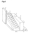
- Fig. 6 is a schematic diagram for explaining migration of charge in a photoelectric converting portion.
- positively ionized donors exist in an n-type semiconductor and negatively ionized acceptors exist in a p-type semiconductor.
- the potential in the n-type semiconductor becomes higher than that in the p-type semiconductor.
- the potential in an energy band diagram is positive in the downward direction and therefore the potential in the n-type semiconductor becomes deeper (or higher) than the potential in the p-type semiconductor in the energy band diagram and has a lower energy level.
- a positive potential is applied to each electrode, a potential of a semiconductor region immediately below the electrode becomes deeper (or increases in the positive direction).
- the magnitude of the positive potential applied to each electrode is reduced, the potential of the semiconductor region immediately below the corresponding electrode becomes shallower (or decreases in the positive direction).
- the signals MGL, MGH, TG1, P1V, P2V, TG2, P1H are L level, whereby the potential ⁇ 32 of the n-type semiconductor layer 32 is deeper than the potential ⁇ 33 of the n - -type semiconductor layer 33, thus forming a well of the potential ⁇ 32 (cf. Fig. 4 (a) ).
- the generated charge is accumulated in the well of the potential ⁇ 32 .
- a charge quantity QL 1 is accumulated in the potential ⁇ 32 .
- the signals MGL, MGH are H level, whereby the potential gradient increasing in the first direction is formed in the n-type semiconductor layer 32 and the potential ⁇ 32 is inclined so as to deepen toward the n - -type semiconductor layer 33, thereby forming the gradient of the potential ⁇ 32 (cf. Fig. 4 (b) ).
- the signals TG1, P2V, TG2 are H level to deepen each of the potentials ⁇ 33 , ⁇ 34 of the n - -type semiconductor layer 33 and the n-type semiconductor layer 34, the potentials ⁇ 37-1 , ⁇ 37-2 , ⁇ 38-1 , ⁇ 38-2 of the n - -type semiconductor layers 37 and the n-type semiconductor layers 38, and the potentials ⁇ 39 , ⁇ 40 of the n - -type semiconductor layer 39 and the n-type semiconductor layer 40, thereby forming respective wells of the potentials ⁇ 34 , ⁇ 38-1 , ⁇ 38-2 , ⁇ 40 .
- the charge C accumulated in the well of the potential ⁇ 32 migrates along the gradient of the potential ⁇ 32 , as also shown in Fig. 5 , to be transferred into the well of the potential ⁇ 34 .
- the charge quantity QL 1 is accumulated in the potential ⁇ 34 .
- the signals MGL, MGH, TG1 are L level to eliminate the gradient of the potential ⁇ 32 and shallow the potentials ⁇ 33 , ⁇ 34 (cf. Fig. 4 (c) ). This causes a generated charge to be accumulated in the well of the potential ⁇ 32 as at time t1.
- a charge quantity QL 2 is accumulated in the potential ⁇ 32 .
- the signals P2V, TG2 are L level and the signal P1V is H level, whereby the potentials ⁇ 37-1 , ⁇ 37-2 , ⁇ 38-1 , ⁇ 38-2 , ⁇ 39 , ⁇ 40 are shallow and the potentials ⁇ 35-1 , ⁇ 35-2 , ⁇ 35-3 , ⁇ 36-1 , ⁇ 36-2 , ⁇ 36-3 of the n - -type semiconductor layers 35 and the n-type semiconductor layers 36 are deep, thus forming respective wells of the potentials ⁇ 36-1 , ⁇ 36-2 , ⁇ 36-3 .
- the charge accumulated in the well of the potential ⁇ 34 is transferred into the well of the potential ⁇ 36-1 .
- the charge quantity QL 1 is accumulated in the potential ⁇ 36-1 .
- the signals MGL, MGH, TG1, P2V, TG2 are H level and the signal P1V is L level, to form the gradient of the potential ⁇ 32 and the respective wells of the potentials ⁇ 34 , ⁇ 38-1 , ⁇ 38-2 , ⁇ 40 as at time t2 (cf. Fig. 4 (d) ).
- the charge accumulated in the well of the potential ⁇ 32 is transferred along the gradient of the potential ⁇ 32 into the well of the potential ⁇ 34 .
- the charge quantity QL 2 is accumulated in the potential ⁇ 34 .
- the charge accumulated in the well of the potential ⁇ 36-1 is transferred into the well of the potential ⁇ 38-1 .
- the charge quantity QL 1 is accumulated in the potential ⁇ 38-1 .
- the signals MGL, MGH, TG1, P2V, TG2 are L level and the signal P1V is H level, to eliminate the gradient of the potential ⁇ 32 and form the respective wells of the potentials ⁇ 36-1 , ⁇ 36-2 , ⁇ 36-3 as at time t3 (cf. Fig. 4 (e) ).
- This causes a generated charge to be accumulated in the well of the potential ⁇ 32 as at times t1 and t3.
- a charge quantity QL 3 is accumulated in the potential ⁇ 32 .
- the charge accumulated in the well of the potential ⁇ 34 is transferred into the well of the potential ⁇ 36-1 .
- the charge quantity QL 2 is accumulated in the potential ⁇ 36-1 .
- the charge accumulated in the well of the potential ⁇ 38-1 is transferred into the well of the potential ⁇ 36-2 .
- the charge quantity QL 1 is accumulated in the potential ⁇ 36-2 .
- the signals MGL, MGH, TG1, P2V, TG2 are H level and the signal P1V is L level, to form the gradient of the potential ⁇ 32 and the respective wells of the potentials ⁇ 34 , ⁇ 38-1 , ⁇ 38-2 , ⁇ 40 as at the times t2 and t4 (cf. Fig. 4 (f) ).
- the charge accumulated in the well of the potential ⁇ 32 is transferred along the gradient of the potential ⁇ 32 into the well of the potential ⁇ 34 .
- the charge quantity QL 3 is accumulated in the potential ⁇ 34 .
- the charge accumulated in the well of the potential ⁇ 36-1 is transferred into the well of the potential ⁇ 38-1 .
- the charge quantity QL 2 is accumulated in the potential ⁇ 38-1 .
- the charge accumulated in the well of the potential ⁇ 36-2 is transferred into the well of the potential ⁇ 38-2 .
- the charge quantity QL 1 is accumulated in the potential ⁇ 38-2 .
- the charge quantity QL 3 is accumulated in the potential ⁇ 36-1 .
- the charge accumulated in the well of the potential ⁇ 38-1 is transferred into the well of the potential ⁇ 36-2 .
- the charge quantity QL 2 is accumulated in the potential ⁇ 36-2 .
- the charge accumulated in the well of the potential ⁇ 38-2 is transferred into the well of the potential ⁇ 36-3 .
- the charge quantity QL 1 is accumulated in the potential ⁇ 36-3 .
- the signals MGL, MGH, TG1, P2V, TG2, P1H are H level and the signals P1V is L level, to form the respective wells of the potentials ⁇ 34 , ⁇ 38-1 , ⁇ 38-2 , ⁇ 40 (cf. Fig. 4 (h) ).
- the charge accumulated in the well of the potential ⁇ 32 is transferred along the gradient of the potential ⁇ 32 into the well of the potential ⁇ 34 .
- the charge quantity QL 4 is accumulated in the potential ⁇ 34 .
- the charge accumulated in the well of the potential ⁇ 36-1 is transferred into the well of the potential ⁇ 38-1 .
- the charge quantity QL 3 is accumulated in the potential ⁇ 38-1 .
- the charge accumulated in the well of the potential ⁇ 36-2 is transferred into the well of the potential ⁇ 38-2 .
- the charge quantity QL 2 is accumulated in the potential ⁇ 38-2 .
- the charge accumulated in the well of the potential ⁇ 36-3 is transferred into the well of the potential ⁇ 40 .
- the charge quantity QL 1 is accumulated in the potential ⁇ 40 . Since at time t8 the signal P1H is H level, the respective potentials ⁇ 41 , ⁇ 42 of the n - -type semiconductor layer 41 and the n-type semiconductor layer 42 are deep to form a well of the potential ⁇ 42 .
- a generated charge is accumulated in the well of the potential ⁇ 32 in the state in which the gradient of the potential ⁇ 32 is formed, as at time t7.
- a charge quantity QL 5 is accumulated in the potential ⁇ 32 (cf. Fig 5 (a) ).
- the respective wells of the potentials ⁇ 36-1 , ⁇ 36-2 , ⁇ 36-3 are formed as at time t7.
- the charge accumulated in the well of the potential ⁇ 34 is transferred into the well of the potential ⁇ 36-1 .
- the charge quantity QL 4 is accumulated in the potential ⁇ 36-1 .
- the charge accumulated in the well of the potential ⁇ 38-1 is transferred into the well of the potential ⁇ 36-2 .
- the charge quantity QL 3 is accumulated in the potential ⁇ 36-2 .
- the charge accumulated in the well of the potential ⁇ 38-2 is transferred into the well of the potential ⁇ 36-3 .
- the charge quantity QL 2 is accumulated in the potential ⁇ 36-3 . Since at time t9 the potentials ⁇ 39 , ⁇ 40 are shallow, the charge accumulated in the well of the potential ⁇ 40 is transferred into the well of the potential ⁇ 42 .
- the charge quantity QL 1 is accumulated in the potential ⁇ 42 .
- the signals MGL, MGH, TG1, P2V, TG2, P1H are H level and the signal P1V is L level, to form the respective wells of the potentials ⁇ 34 , ⁇ 38-1 , ⁇ 38-2 , ⁇ 40 as at time t8 (cf. Fig. 5 (b) ).
- the charge accumulated in the well of the potential ⁇ 32 is transferred along the gradient of the potential ⁇ 32 into the well of the potential ⁇ 34 .
- the charge quantity QL 5 is accumulated in the potential ⁇ 34 .
- the charge accumulated in the well of the potential ⁇ 36-1 is transferred into the well of the potential ⁇ 38-1 .
- the charge quantity QL 4 is accumulated in the potential ⁇ 38-1 .
- the charge accumulated in the well of the potential ⁇ 36-2 is transferred into the well of the potential ⁇ 38-2 .
- the charge quantity QL 3 is accumulated in the potential ⁇ 38-2 .
- the charge accumulated in the well of the potential ⁇ 36-3 is transferred into the well of the potential ⁇ 40 .
- the charge quantity QL 2 is accumulated in the potential ⁇ 40 .
- the charge quantity QL 5 is accumulated in the potential ⁇ 36-1 .
- the charge accumulated in the well of the potential ⁇ 38-1 is transferred into the well of the potential ⁇ 36-2 .
- the charge quantity QL 4 is accumulated in the potential ⁇ 36-2 .
- the charge accumulated in the well of the potential ⁇ 38-2 is transferred into the well of the potential ⁇ 36-3 .
- the charge quantity QL 3 is accumulated in the potential ⁇ 36-3 .
- the charge accumulated in the well of the potential ⁇ 40 is transferred into the well of the potential ⁇ 42 .
- the charge quantity QL 1 plus the charge quantity QL 2 are accumulated in the potential ⁇ 42 .
- the signals MGL, MGH, TG1, P2V, TG2, P1H are H level and the signal P1V is L level, to form the respective wells of the potentials ⁇ 34 , ⁇ 38-1 , ⁇ 38-2 , ⁇ 40 as at time t8 (cf. Fig. 5 (d) ).
- the charge accumulated in the well of the potential ⁇ 32 is transferred along the gradient of the potential ⁇ 32 into the well of the potential ⁇ 34 .
- the charge quantity QL 6 is accumulated in the potential ⁇ 34 .
- the charge accumulated in the well of the potential ⁇ 36-1 is transferred into the well of the potential ⁇ 38-1 .
- the charge quantity QL 5 is accumulated in the potential ⁇ 38-1 .
- the charge accumulated in the well of the potential ⁇ 36-2 is transferred into the well of the potential ⁇ 38-2 .
- the charge quantity QL 4 is accumulated in the potential ⁇ 38-2 .
- the charge accumulated in the well of the potential ⁇ 36-3 is transferred into the well of the potential ⁇ 40 .
- the charge quantity QL 3 is accumulated in the potential ⁇ 40.
- the signals MGL, MGH, TG1, P2V, TG2 are L level and the signal P1V is H level, to eliminate the gradient of the potential ⁇ 32 and to accumulate a newly generated charge in the well of the potential ⁇ 32 (cf. Fig. 5 (e) ).
- the respective wells of the potentials ⁇ 36-1 , ⁇ 36-2 , ⁇ 36-3 are formed as at time t9.
- the charge accumulated in the well of the potential ⁇ 34 is transferred into the well of the potential ⁇ 36-1 .
- the charge quantity QL 6 is accumulated in the potential ⁇ 36-1 .
- the charge accumulated in the well of the potential ⁇ 38-1 is transferred into the well of the potential ⁇ 36-2 .
- the charge quantity QL 5 is accumulated in the potential ⁇ 36-2 .
- the charge accumulated in the well of the potential ⁇ 338-2 is transferred into the well of the potential ⁇ 36-3 .
- the charge quantity QL 4 is accumulated in the potential ⁇ 36-3 .
- the charge accumulated in the well of the potential ⁇ 40 is transferred into the well of the potential ⁇ 42 .
- the sum of the charge quantities QL 1 , QL 2 , QL 3 is accumulated in the potential ⁇ 42 .
- the charge in the sum of the charge quantities QL 1 , QL 2 , QL 3 is sequentially transferred in the second direction during a charge transferring period TP1 to be output to the amplifier portion 21.
- a signal for transferring the sum of charge quantities QL 1 , QL 2 , QL 3 in the second direction is given as signal P1H during the charge transferring period TP 1.
- the signal P1H is H level and in which the signals MGL, MGH, TG1 are L level
- the signal P1V is L level and the signals P2V, TG2 are H level
- the charge accumulated in the well of the potential ⁇ 36-1 is transferred into the well of the potential ⁇ 38-1 .
- the charge quantity QL 6 is accumulated in the potential ⁇ 38-1 .
- the charge accumulated in the well of the potential ⁇ 36-2 is transferred into the well of the potential ⁇ 38-2 .
- the charge quantity QL 5 is accumulated in the potential ⁇ 38-2 .
- the charge accumulated in the well of the potential ⁇ 36-3 is transferred into the well of the potential ⁇ 40 .
- the charge quantity QL 4 is accumulated in the potential ⁇ 40 .
- the signals P2V, TG2 are L level and the signal P1V is H level, to form the respective wells of the potentials ⁇ 36-1 , ⁇ 36-2 , ⁇ 36-3 (cf. Fig. 5 (g) ).
- the charge accumulated in the well of the potential ⁇ 38-1 is transferred into the well of the potential ⁇ 36-2 .
- the charge quantity QL 6 is accumulated in the potential ⁇ 36-2 .
- the charge accumulated in the well of the potential ⁇ 38-2 is transferred into the well of the potential ⁇ 36-3 .
- the charge quantity QL 5 is accumulated in the potential ⁇ 36-3 .
- the charge accumulated in the well of the potential ⁇ 40 is transferred into the well of the potential ⁇ 42 .
- the charge quantity QL 4 is accumulated in the potential ⁇ 42 .
- the planar shape of the photosensitive region 13 is the nearly rectangular shape composed of two long sides and two short sides.
- the length in the long side direction of the photosensitive region 13 can be made long to increase a saturated charge quantity in each photosensitive region 13, thereby enabling an improvement in SN ratio.
- the plurality of photoelectric converting portions 3 are juxtaposed along the second direction intersecting with the first direction and are arranged in the array form in the one-dimensional direction.
- the plurality of photoelectric converting portions 3 are juxtaposed in the direction along the short side direction of the photosensitive region 13. Since in each photoelectric converting portion 3 the potential gradient increasing along the first direction is formed by the electrode 51, the charge generated in the photosensitive region 13 migrates toward the other short side along the slope of potential according to the potential gradient formed. The charge having migrated to the other short side is acquired by the first transferring portion 5 to be transferred in the first direction. This makes the charge migration speed dominated by the potential gradient (slope of potential), so as to increase the charge readout speed.
- the charge transferred from the first transferring portion 5 is accumulated in the charge accumulating portion 7 and then is transferred in the first direction by the second transferring portion 9. Then the charges transferred from the respective second transferring portions 9 are transferred in the second direction and output by the shift register 11.
- the solid-state imaging device 1 does not have to execute further signal processing for obtaining a one-dimensional image, whereby the image processing can be prevented from becoming complicated.
- the photosensitive region 13 has the planar shape of the nearly rectangular shape composed of two long sides and two short sides. As a result of this, the saturated charge quantity in the photosensitive region 13 is large.
- the sum of the first period T1 and the second period T2 is defined as one readout period, in which charges generated in the photoelectric converting portion 3 are accumulated and output.
- the charge generated in the photoelectric converting portion 3 during the first period is read out in the charge transferring period TP1 and the charge generated in the photoelectric converting portion 3 during the second period is read out in the charge transferring period TP2.
- the first period T1 is set, for example, at about 9.99 ms
- the second period T2 is set, for example, at about 10 ⁇ s
- the first period T1 is approximately 1000 times the second period T2.
- the output from the solid-state imaging device 1 may be defined as 1000 times an output based on the charge quantity generated in the photoelectric converting portion 3 during the second period T2. If the charge quantity generated in the photoelectric converting portion 3 during the first period T1 is not saturated, the output from the solid-state imaging device 1 may be defined as an output based on the sum of the charge quantity generated in the photoelectric converting portion 3 during the first period T1 and the charge quantity generated in the photoelectric converting portion 3 during the second period T2.
- the solid-state imaging device 1 When the charge generated in the photoelectric converting portion 3 during the first period T1 is accumulated, since the exposure time is relatively long, strong incident light results in saturation of a signal and this makes appropriate detection difficult. In contrast to it, weak incident light is detected as a sufficiently large signal. On the other hand, when the charge generated in the photoelectric converting portion 3 during the second period T2 is accumulated, since the exposure time is relatively short, weak incident light results in a very weak signal and this makes sufficient signal detection difficult. In contrast to it, strong incident light is appropriately detected as a signal, without saturation. As described above, the solid-state imaging device 1 appropriately detects the incident light as a signal, regardless of the intensity of incident light, so as to increase the effective dynamic range.
- the device is provided with the charge accumulating portions 7. This allows the charge generated in the photoelectric converting portion 3 during the first period T1 to be accumulated and transferred through the second transferring portion 9 to the shift register 11 so as to cause no impediment in transferring the charge generated in the photoelectric converting portion 3 during the second period T2.
- the present invention is applicable to the light detecting means of the spectroscope.
Landscapes
- Engineering & Computer Science (AREA)
- Multimedia (AREA)
- Signal Processing (AREA)
- Physics & Mathematics (AREA)
- Power Engineering (AREA)
- Electromagnetism (AREA)
- Condensed Matter Physics & Semiconductors (AREA)
- General Physics & Mathematics (AREA)
- Computer Hardware Design (AREA)
- Microelectronics & Electronic Packaging (AREA)
- Solid State Image Pick-Up Elements (AREA)
- Transforming Light Signals Into Electric Signals (AREA)
Applications Claiming Priority (2)
| Application Number | Priority Date | Filing Date | Title |
|---|---|---|---|
| JP2008078598A JP5350659B2 (ja) | 2008-03-25 | 2008-03-25 | 固体撮像装置 |
| PCT/JP2009/055809 WO2009119573A1 (ja) | 2008-03-25 | 2009-03-24 | 固体撮像装置 |
Publications (3)
| Publication Number | Publication Date |
|---|---|
| EP2273551A1 true EP2273551A1 (de) | 2011-01-12 |
| EP2273551A4 EP2273551A4 (de) | 2012-05-02 |
| EP2273551B1 EP2273551B1 (de) | 2016-12-28 |
Family
ID=41113765
Family Applications (1)
| Application Number | Title | Priority Date | Filing Date |
|---|---|---|---|
| EP09724745.6A Active EP2273551B1 (de) | 2008-03-25 | 2009-03-24 | Halbleiterabbildungsvorrichtung |
Country Status (6)
| Country | Link |
|---|---|
| US (1) | US8415604B2 (de) |
| EP (1) | EP2273551B1 (de) |
| JP (1) | JP5350659B2 (de) |
| KR (1) | KR101588907B1 (de) |
| CN (1) | CN101981698B (de) |
| WO (1) | WO2009119573A1 (de) |
Cited By (4)
| Publication number | Priority date | Publication date | Assignee | Title |
|---|---|---|---|---|
| CN103314441A (zh) * | 2011-01-14 | 2013-09-18 | 浜松光子学株式会社 | 固体摄像装置 |
| US9419051B2 (en) | 2011-01-20 | 2016-08-16 | Hamamatsu Photonics K.K. | Solid-state imaging device |
| EP3067934A4 (de) * | 2013-11-05 | 2017-07-05 | Hamamatsu Photonics K.K. | Linearer bildsensor |
| EP3190622A4 (de) * | 2014-09-01 | 2018-04-25 | Hamamatsu Photonics K.K. | Festkörperbildgebungsvorrichtung |
Citations (6)
| Publication number | Priority date | Publication date | Assignee | Title |
|---|---|---|---|---|
| JPH06283704A (ja) * | 1993-03-24 | 1994-10-07 | Sony Corp | Ccd型固体撮像素子 |
| JPH1127476A (ja) * | 1997-07-02 | 1999-01-29 | Sony Corp | 固体撮像装置 |
| US5949099A (en) * | 1995-03-15 | 1999-09-07 | Sony Corporation | Solid-state image sensing device and its driving method |
| US20020057356A1 (en) * | 1996-12-18 | 2002-05-16 | Akihito Tanabe | Solid-state image pickup device having vertical overflow drain and resistive gate charge transfer device and method of controlling thereof |
| EP1583150A1 (de) * | 2004-03-31 | 2005-10-05 | CSEM Centre Suisse d'Electronique et de Microtechnique SA | Bildsensor mit grossflächigen, hochgeschwindigen, hochempfindlichen Pixeln |
| EP1619723A1 (de) * | 2003-04-23 | 2006-01-25 | Hamamatsu Photonics K. K. | Röhrenlose abbildungseinrichtung |
Family Cites Families (14)
| Publication number | Priority date | Publication date | Assignee | Title |
|---|---|---|---|---|
| JPS5424530A (en) * | 1977-07-26 | 1979-02-23 | Matsushita Electronics Corp | Solidstate pick up unit |
| US4176369A (en) * | 1977-12-05 | 1979-11-27 | Rockwell International Corporation | Image sensor having improved moving target discernment capabilities |
| JP2526953B2 (ja) * | 1987-12-25 | 1996-08-21 | 株式会社ニコン | 焦点検出装置 |
| DE69508345T2 (de) * | 1994-11-12 | 1999-10-07 | Sony Corp | Ansteuerverfahren einer CCD Festkörper-Bildaufnahmevorrichtung und Videokamera nach dem Verfahren |
| JPH08279608A (ja) * | 1995-04-06 | 1996-10-22 | Sony Corp | 電荷転送素子及び電荷転送素子の駆動方法 |
| JP2000164847A (ja) * | 1998-11-27 | 2000-06-16 | Nikon Corp | イメージセンサーおよびイメージセンサーシステム |
| JP2001119005A (ja) * | 1999-10-18 | 2001-04-27 | Yokogawa Electric Corp | フォトダイオードアレイ |
| JP2002231926A (ja) * | 2001-02-01 | 2002-08-16 | Fuji Photo Film Co Ltd | ラインセンサおよびそれを用いた放射線画像情報読取装置 |
| JP3995983B2 (ja) * | 2002-05-22 | 2007-10-24 | 松下電器産業株式会社 | 固体撮像装置の駆動方法、信号処理方法および基板電圧調整方法 |
| JP4625605B2 (ja) | 2002-06-28 | 2011-02-02 | 富士フイルム株式会社 | 固体撮像装置 |
| JP2005164363A (ja) * | 2003-12-02 | 2005-06-23 | Shimadzu Corp | 受光素子、および、この素子を用いた受光素子アレイ |
| JP2005268564A (ja) * | 2004-03-19 | 2005-09-29 | Ricoh Co Ltd | 固体撮像素子及び固体撮像素子の製造方法 |
| JP2007036714A (ja) * | 2005-07-27 | 2007-02-08 | Hitachi Ltd | 撮像装置 |
| JP2008034949A (ja) * | 2006-07-26 | 2008-02-14 | Matsushita Electric Ind Co Ltd | 固体撮像装置の駆動方法、及び固体撮像装置 |
-
2008
- 2008-03-25 JP JP2008078598A patent/JP5350659B2/ja active Active
-
2009
- 2009-03-24 US US12/933,992 patent/US8415604B2/en active Active
- 2009-03-24 WO PCT/JP2009/055809 patent/WO2009119573A1/ja active Application Filing
- 2009-03-24 KR KR1020107010496A patent/KR101588907B1/ko active IP Right Grant
- 2009-03-24 EP EP09724745.6A patent/EP2273551B1/de active Active
- 2009-03-24 CN CN200980111025.6A patent/CN101981698B/zh active Active
Patent Citations (6)
| Publication number | Priority date | Publication date | Assignee | Title |
|---|---|---|---|---|
| JPH06283704A (ja) * | 1993-03-24 | 1994-10-07 | Sony Corp | Ccd型固体撮像素子 |
| US5949099A (en) * | 1995-03-15 | 1999-09-07 | Sony Corporation | Solid-state image sensing device and its driving method |
| US20020057356A1 (en) * | 1996-12-18 | 2002-05-16 | Akihito Tanabe | Solid-state image pickup device having vertical overflow drain and resistive gate charge transfer device and method of controlling thereof |
| JPH1127476A (ja) * | 1997-07-02 | 1999-01-29 | Sony Corp | 固体撮像装置 |
| EP1619723A1 (de) * | 2003-04-23 | 2006-01-25 | Hamamatsu Photonics K. K. | Röhrenlose abbildungseinrichtung |
| EP1583150A1 (de) * | 2004-03-31 | 2005-10-05 | CSEM Centre Suisse d'Electronique et de Microtechnique SA | Bildsensor mit grossflächigen, hochgeschwindigen, hochempfindlichen Pixeln |
Non-Patent Citations (1)
| Title |
|---|
| See also references of WO2009119573A1 * |
Cited By (8)
| Publication number | Priority date | Publication date | Assignee | Title |
|---|---|---|---|---|
| CN103314441A (zh) * | 2011-01-14 | 2013-09-18 | 浜松光子学株式会社 | 固体摄像装置 |
| CN103314441B (zh) * | 2011-01-14 | 2016-01-27 | 浜松光子学株式会社 | 固体摄像装置 |
| US9419051B2 (en) | 2011-01-20 | 2016-08-16 | Hamamatsu Photonics K.K. | Solid-state imaging device |
| EP2667410A4 (de) * | 2011-01-20 | 2017-09-06 | Hamamatsu Photonics K.K. | Festkörperabbildungsvorrichtung |
| EP3067934A4 (de) * | 2013-11-05 | 2017-07-05 | Hamamatsu Photonics K.K. | Linearer bildsensor |
| US10403677B2 (en) | 2013-11-05 | 2019-09-03 | Hamamatsu Photonics K.K. | Linear image sensor |
| EP3190622A4 (de) * | 2014-09-01 | 2018-04-25 | Hamamatsu Photonics K.K. | Festkörperbildgebungsvorrichtung |
| US10483302B2 (en) | 2014-09-01 | 2019-11-19 | Hamamatsu Photonics K.K. | Solid-state imaging device |
Also Published As
| Publication number | Publication date |
|---|---|
| US8415604B2 (en) | 2013-04-09 |
| KR20100133355A (ko) | 2010-12-21 |
| CN101981698A (zh) | 2011-02-23 |
| WO2009119573A1 (ja) | 2009-10-01 |
| JP2009231768A (ja) | 2009-10-08 |
| CN101981698B (zh) | 2014-11-26 |
| EP2273551A4 (de) | 2012-05-02 |
| JP5350659B2 (ja) | 2013-11-27 |
| KR101588907B1 (ko) | 2016-01-26 |
| US20110024607A1 (en) | 2011-02-03 |
| EP2273551B1 (de) | 2016-12-28 |
Similar Documents
| Publication | Publication Date | Title |
|---|---|---|
| EP2284898B1 (de) | Festkörperabbildungseinrichtung | |
| EP2667410B1 (de) | Festkörperabbildungsvorrichtung | |
| US9653514B2 (en) | Solid-state imaging device and method for driving the same | |
| KR101335142B1 (ko) | 고체 촬상 장치 | |
| US9905608B1 (en) | EMCCD image sensor with stable charge multiplication gain | |
| US4589003A (en) | Solid state image sensor comprising photoelectric converting film and reading-out transistor | |
| US9299860B2 (en) | Solid state imaging device including photoelectric conversion portion | |
| US8415604B2 (en) | Solid-state imaging device | |
| JPH0360159A (ja) | 固体撮像素子 | |
| US4616249A (en) | Solid state image pick-up element of static induction transistor type | |
| US7750376B2 (en) | Solid-state imaging device and imaging apparatus | |
| JPH0471341B2 (de) | ||
| JP2000214202A (ja) | 電荷検出装置 | |
| CN115516635A (zh) | 光检测装置和光传感器的驱动方法 | |
| CN114830632A (zh) | 光检测装置和光传感器的驱动方法 | |
| JPH04130666A (ja) | 固体撮像素子 | |
| JPS62293672A (ja) | 固体撮像素子 | |
| JPS634681A (ja) | 半導体装置 | |
| JPH0248875A (ja) | 固体撮像装置の駆動方法 | |
| JPH04346445A (ja) | 固体撮像装置 | |
| JPS5976464A (ja) | 固体イメ−ジセンサ | |
| JPS63318155A (ja) | 固体撮像素子 | |
| JPS60137165A (ja) | 固体撮像装置 |
Legal Events
| Date | Code | Title | Description |
|---|---|---|---|
| PUAI | Public reference made under article 153(3) epc to a published international application that has entered the european phase |
Free format text: ORIGINAL CODE: 0009012 |
|
| 17P | Request for examination filed |
Effective date: 20101019 |
|
| AK | Designated contracting states |
Kind code of ref document: A1 Designated state(s): AT BE BG CH CY CZ DE DK EE ES FI FR GB GR HR HU IE IS IT LI LT LU LV MC MK MT NL NO PL PT RO SE SI SK TR |
|
| AX | Request for extension of the european patent |
Extension state: AL BA RS |
|
| DAX | Request for extension of the european patent (deleted) | ||
| A4 | Supplementary search report drawn up and despatched |
Effective date: 20120402 |
|
| RIC1 | Information provided on ipc code assigned before grant |
Ipc: H04N 5/335 20110101ALI20120327BHEP Ipc: H01L 27/148 20060101AFI20120327BHEP |
|
| 17Q | First examination report despatched |
Effective date: 20130812 |
|
| RIC1 | Information provided on ipc code assigned before grant |
Ipc: G01J 3/28 20060101AFI20160614BHEP Ipc: H04N 5/335 20060101ALI20160614BHEP Ipc: H01L 27/148 20060101ALI20160614BHEP |
|
| GRAP | Despatch of communication of intention to grant a patent |
Free format text: ORIGINAL CODE: EPIDOSNIGR1 |
|
| RIC1 | Information provided on ipc code assigned before grant |
Ipc: G01J 3/28 20060101ALI20160707BHEP Ipc: H04N 5/369 20110101ALI20160707BHEP Ipc: H01L 27/148 20060101AFI20160707BHEP Ipc: H04N 5/335 20060101ALI20160707BHEP |
|
| INTG | Intention to grant announced |
Effective date: 20160726 |
|
| GRAS | Grant fee paid |
Free format text: ORIGINAL CODE: EPIDOSNIGR3 |
|
| GRAA | (expected) grant |
Free format text: ORIGINAL CODE: 0009210 |
|
| AK | Designated contracting states |
Kind code of ref document: B1 Designated state(s): AT BE BG CH CY CZ DE DK EE ES FI FR GB GR HR HU IE IS IT LI LT LU LV MC MK MT NL NO PL PT RO SE SI SK TR |
|
| REG | Reference to a national code |
Ref country code: GB Ref legal event code: FG4D |
|
| REG | Reference to a national code |
Ref country code: CH Ref legal event code: EP |
|
| REG | Reference to a national code |
Ref country code: AT Ref legal event code: REF Ref document number: 857959 Country of ref document: AT Kind code of ref document: T Effective date: 20170115 |
|
| REG | Reference to a national code |
Ref country code: IE Ref legal event code: FG4D |
|
| REG | Reference to a national code |
Ref country code: FR Ref legal event code: PLFP Year of fee payment: 9 |
|
| REG | Reference to a national code |
Ref country code: DE Ref legal event code: R096 Ref document number: 602009043372 Country of ref document: DE |
|
| PG25 | Lapsed in a contracting state [announced via postgrant information from national office to epo] |
Ref country code: LV Free format text: LAPSE BECAUSE OF FAILURE TO SUBMIT A TRANSLATION OF THE DESCRIPTION OR TO PAY THE FEE WITHIN THE PRESCRIBED TIME-LIMIT Effective date: 20161228 |
|
| REG | Reference to a national code |
Ref country code: LT Ref legal event code: MG4D |
|
| PG25 | Lapsed in a contracting state [announced via postgrant information from national office to epo] |
Ref country code: NO Free format text: LAPSE BECAUSE OF FAILURE TO SUBMIT A TRANSLATION OF THE DESCRIPTION OR TO PAY THE FEE WITHIN THE PRESCRIBED TIME-LIMIT Effective date: 20170328 Ref country code: GR Free format text: LAPSE BECAUSE OF FAILURE TO SUBMIT A TRANSLATION OF THE DESCRIPTION OR TO PAY THE FEE WITHIN THE PRESCRIBED TIME-LIMIT Effective date: 20170329 Ref country code: SE Free format text: LAPSE BECAUSE OF FAILURE TO SUBMIT A TRANSLATION OF THE DESCRIPTION OR TO PAY THE FEE WITHIN THE PRESCRIBED TIME-LIMIT Effective date: 20161228 Ref country code: LT Free format text: LAPSE BECAUSE OF FAILURE TO SUBMIT A TRANSLATION OF THE DESCRIPTION OR TO PAY THE FEE WITHIN THE PRESCRIBED TIME-LIMIT Effective date: 20161228 |
|
| REG | Reference to a national code |
Ref country code: NL Ref legal event code: MP Effective date: 20161228 |
|
| REG | Reference to a national code |
Ref country code: AT Ref legal event code: MK05 Ref document number: 857959 Country of ref document: AT Kind code of ref document: T Effective date: 20161228 |
|
| PG25 | Lapsed in a contracting state [announced via postgrant information from national office to epo] |
Ref country code: HR Free format text: LAPSE BECAUSE OF FAILURE TO SUBMIT A TRANSLATION OF THE DESCRIPTION OR TO PAY THE FEE WITHIN THE PRESCRIBED TIME-LIMIT Effective date: 20161228 Ref country code: FI Free format text: LAPSE BECAUSE OF FAILURE TO SUBMIT A TRANSLATION OF THE DESCRIPTION OR TO PAY THE FEE WITHIN THE PRESCRIBED TIME-LIMIT Effective date: 20161228 |
|
| PG25 | Lapsed in a contracting state [announced via postgrant information from national office to epo] |
Ref country code: NL Free format text: LAPSE BECAUSE OF FAILURE TO SUBMIT A TRANSLATION OF THE DESCRIPTION OR TO PAY THE FEE WITHIN THE PRESCRIBED TIME-LIMIT Effective date: 20161228 |
|
| PG25 | Lapsed in a contracting state [announced via postgrant information from national office to epo] |
Ref country code: SK Free format text: LAPSE BECAUSE OF FAILURE TO SUBMIT A TRANSLATION OF THE DESCRIPTION OR TO PAY THE FEE WITHIN THE PRESCRIBED TIME-LIMIT Effective date: 20161228 Ref country code: IS Free format text: LAPSE BECAUSE OF FAILURE TO SUBMIT A TRANSLATION OF THE DESCRIPTION OR TO PAY THE FEE WITHIN THE PRESCRIBED TIME-LIMIT Effective date: 20170428 Ref country code: CZ Free format text: LAPSE BECAUSE OF FAILURE TO SUBMIT A TRANSLATION OF THE DESCRIPTION OR TO PAY THE FEE WITHIN THE PRESCRIBED TIME-LIMIT Effective date: 20161228 Ref country code: EE Free format text: LAPSE BECAUSE OF FAILURE TO SUBMIT A TRANSLATION OF THE DESCRIPTION OR TO PAY THE FEE WITHIN THE PRESCRIBED TIME-LIMIT Effective date: 20161228 Ref country code: RO Free format text: LAPSE BECAUSE OF FAILURE TO SUBMIT A TRANSLATION OF THE DESCRIPTION OR TO PAY THE FEE WITHIN THE PRESCRIBED TIME-LIMIT Effective date: 20161228 |
|
| PG25 | Lapsed in a contracting state [announced via postgrant information from national office to epo] |
Ref country code: PL Free format text: LAPSE BECAUSE OF FAILURE TO SUBMIT A TRANSLATION OF THE DESCRIPTION OR TO PAY THE FEE WITHIN THE PRESCRIBED TIME-LIMIT Effective date: 20161228 Ref country code: BG Free format text: LAPSE BECAUSE OF FAILURE TO SUBMIT A TRANSLATION OF THE DESCRIPTION OR TO PAY THE FEE WITHIN THE PRESCRIBED TIME-LIMIT Effective date: 20170328 Ref country code: BE Free format text: LAPSE BECAUSE OF FAILURE TO SUBMIT A TRANSLATION OF THE DESCRIPTION OR TO PAY THE FEE WITHIN THE PRESCRIBED TIME-LIMIT Effective date: 20161228 Ref country code: PT Free format text: LAPSE BECAUSE OF FAILURE TO SUBMIT A TRANSLATION OF THE DESCRIPTION OR TO PAY THE FEE WITHIN THE PRESCRIBED TIME-LIMIT Effective date: 20170428 Ref country code: IT Free format text: LAPSE BECAUSE OF FAILURE TO SUBMIT A TRANSLATION OF THE DESCRIPTION OR TO PAY THE FEE WITHIN THE PRESCRIBED TIME-LIMIT Effective date: 20161228 Ref country code: AT Free format text: LAPSE BECAUSE OF FAILURE TO SUBMIT A TRANSLATION OF THE DESCRIPTION OR TO PAY THE FEE WITHIN THE PRESCRIBED TIME-LIMIT Effective date: 20161228 Ref country code: ES Free format text: LAPSE BECAUSE OF FAILURE TO SUBMIT A TRANSLATION OF THE DESCRIPTION OR TO PAY THE FEE WITHIN THE PRESCRIBED TIME-LIMIT Effective date: 20161228 |
|
| REG | Reference to a national code |
Ref country code: DE Ref legal event code: R097 Ref document number: 602009043372 Country of ref document: DE |
|
| REG | Reference to a national code |
Ref country code: CH Ref legal event code: PL |
|
| PLBE | No opposition filed within time limit |
Free format text: ORIGINAL CODE: 0009261 |
|
| STAA | Information on the status of an ep patent application or granted ep patent |
Free format text: STATUS: NO OPPOSITION FILED WITHIN TIME LIMIT |
|
| PG25 | Lapsed in a contracting state [announced via postgrant information from national office to epo] |
Ref country code: DK Free format text: LAPSE BECAUSE OF FAILURE TO SUBMIT A TRANSLATION OF THE DESCRIPTION OR TO PAY THE FEE WITHIN THE PRESCRIBED TIME-LIMIT Effective date: 20161228 Ref country code: MC Free format text: LAPSE BECAUSE OF FAILURE TO SUBMIT A TRANSLATION OF THE DESCRIPTION OR TO PAY THE FEE WITHIN THE PRESCRIBED TIME-LIMIT Effective date: 20161228 |
|
| 26N | No opposition filed |
Effective date: 20170929 |
|
| REG | Reference to a national code |
Ref country code: IE Ref legal event code: MM4A |
|
| PG25 | Lapsed in a contracting state [announced via postgrant information from national office to epo] |
Ref country code: LU Free format text: LAPSE BECAUSE OF NON-PAYMENT OF DUE FEES Effective date: 20170324 |
|
| REG | Reference to a national code |
Ref country code: FR Ref legal event code: PLFP Year of fee payment: 10 |
|
| PG25 | Lapsed in a contracting state [announced via postgrant information from national office to epo] |
Ref country code: IE Free format text: LAPSE BECAUSE OF NON-PAYMENT OF DUE FEES Effective date: 20170324 Ref country code: SI Free format text: LAPSE BECAUSE OF FAILURE TO SUBMIT A TRANSLATION OF THE DESCRIPTION OR TO PAY THE FEE WITHIN THE PRESCRIBED TIME-LIMIT Effective date: 20161228 Ref country code: CH Free format text: LAPSE BECAUSE OF NON-PAYMENT OF DUE FEES Effective date: 20170331 Ref country code: LI Free format text: LAPSE BECAUSE OF NON-PAYMENT OF DUE FEES Effective date: 20170331 |
|
| PG25 | Lapsed in a contracting state [announced via postgrant information from national office to epo] |
Ref country code: MT Free format text: LAPSE BECAUSE OF NON-PAYMENT OF DUE FEES Effective date: 20170324 |
|
| PG25 | Lapsed in a contracting state [announced via postgrant information from national office to epo] |
Ref country code: HU Free format text: LAPSE BECAUSE OF FAILURE TO SUBMIT A TRANSLATION OF THE DESCRIPTION OR TO PAY THE FEE WITHIN THE PRESCRIBED TIME-LIMIT; INVALID AB INITIO Effective date: 20090324 |
|
| PG25 | Lapsed in a contracting state [announced via postgrant information from national office to epo] |
Ref country code: CY Free format text: LAPSE BECAUSE OF NON-PAYMENT OF DUE FEES Effective date: 20161228 |
|
| PG25 | Lapsed in a contracting state [announced via postgrant information from national office to epo] |
Ref country code: MK Free format text: LAPSE BECAUSE OF FAILURE TO SUBMIT A TRANSLATION OF THE DESCRIPTION OR TO PAY THE FEE WITHIN THE PRESCRIBED TIME-LIMIT Effective date: 20161228 |
|
| PG25 | Lapsed in a contracting state [announced via postgrant information from national office to epo] |
Ref country code: TR Free format text: LAPSE BECAUSE OF FAILURE TO SUBMIT A TRANSLATION OF THE DESCRIPTION OR TO PAY THE FEE WITHIN THE PRESCRIBED TIME-LIMIT Effective date: 20161228 |
|
| PGFP | Annual fee paid to national office [announced via postgrant information from national office to epo] |
Ref country code: FR Payment date: 20230208 Year of fee payment: 15 |
|
| P01 | Opt-out of the competence of the unified patent court (upc) registered |
Effective date: 20230509 |
|
| PGFP | Annual fee paid to national office [announced via postgrant information from national office to epo] |
Ref country code: DE Payment date: 20240130 Year of fee payment: 16 Ref country code: GB Payment date: 20240201 Year of fee payment: 16 |