EP2254393B1 - Light emitting device including semiconductor nanocrystals - Google Patents
Light emitting device including semiconductor nanocrystals Download PDFInfo
- Publication number
- EP2254393B1 EP2254393B1 EP10164996.0A EP10164996A EP2254393B1 EP 2254393 B1 EP2254393 B1 EP 2254393B1 EP 10164996 A EP10164996 A EP 10164996A EP 2254393 B1 EP2254393 B1 EP 2254393B1
- Authority
- EP
- European Patent Office
- Prior art keywords
- electrode
- light emitting
- semiconductor nanocrystals
- substrate
- applicator
- Prior art date
- Legal status (The legal status is an assumption and is not a legal conclusion. Google has not performed a legal analysis and makes no representation as to the accuracy of the status listed.)
- Expired - Lifetime
Links
Images


Classifications
-
- B—PERFORMING OPERATIONS; TRANSPORTING
- B41—PRINTING; LINING MACHINES; TYPEWRITERS; STAMPS
- B41J—TYPEWRITERS; SELECTIVE PRINTING MECHANISMS, i.e. MECHANISMS PRINTING OTHERWISE THAN FROM A FORME; CORRECTION OF TYPOGRAPHICAL ERRORS
- B41J2/00—Typewriters or selective printing mechanisms characterised by the printing or marking process for which they are designed
- B41J2/005—Typewriters or selective printing mechanisms characterised by the printing or marking process for which they are designed characterised by bringing liquid or particles selectively into contact with a printing material
- B41J2/0057—Typewriters or selective printing mechanisms characterised by the printing or marking process for which they are designed characterised by bringing liquid or particles selectively into contact with a printing material where an intermediate transfer member receives the ink before transferring it on the printing material
-
- B—PERFORMING OPERATIONS; TRANSPORTING
- B41—PRINTING; LINING MACHINES; TYPEWRITERS; STAMPS
- B41J—TYPEWRITERS; SELECTIVE PRINTING MECHANISMS, i.e. MECHANISMS PRINTING OTHERWISE THAN FROM A FORME; CORRECTION OF TYPOGRAPHICAL ERRORS
- B41J2/00—Typewriters or selective printing mechanisms characterised by the printing or marking process for which they are designed
- B41J2/005—Typewriters or selective printing mechanisms characterised by the printing or marking process for which they are designed characterised by bringing liquid or particles selectively into contact with a printing material
- B41J2/01—Ink jet
-
- B—PERFORMING OPERATIONS; TRANSPORTING
- B41—PRINTING; LINING MACHINES; TYPEWRITERS; STAMPS
- B41M—PRINTING, DUPLICATING, MARKING, OR COPYING PROCESSES; COLOUR PRINTING
- B41M1/00—Inking and printing with a printer's forme
- B41M1/02—Letterpress printing, e.g. book printing
-
- B—PERFORMING OPERATIONS; TRANSPORTING
- B41—PRINTING; LINING MACHINES; TYPEWRITERS; STAMPS
- B41M—PRINTING, DUPLICATING, MARKING, OR COPYING PROCESSES; COLOUR PRINTING
- B41M3/00—Printing processes to produce particular kinds of printed work, e.g. patterns
- B41M3/003—Printing processes to produce particular kinds of printed work, e.g. patterns on optical devices, e.g. lens elements; for the production of optical devices
-
- B—PERFORMING OPERATIONS; TRANSPORTING
- B41—PRINTING; LINING MACHINES; TYPEWRITERS; STAMPS
- B41M—PRINTING, DUPLICATING, MARKING, OR COPYING PROCESSES; COLOUR PRINTING
- B41M5/00—Duplicating or marking methods; Sheet materials for use therein
- B41M5/025—Duplicating or marking methods; Sheet materials for use therein by transferring ink from the master sheet
- B41M5/0256—Duplicating or marking methods; Sheet materials for use therein by transferring ink from the master sheet the transferable ink pattern being obtained by means of a computer driven printer, e.g. an ink jet or laser printer, or by electrographic means
-
- B—PERFORMING OPERATIONS; TRANSPORTING
- B82—NANOTECHNOLOGY
- B82Y—SPECIFIC USES OR APPLICATIONS OF NANOSTRUCTURES; MEASUREMENT OR ANALYSIS OF NANOSTRUCTURES; MANUFACTURE OR TREATMENT OF NANOSTRUCTURES
- B82Y30/00—Nanotechnology for materials or surface science, e.g. nanocomposites
-
- H—ELECTRICITY
- H05—ELECTRIC TECHNIQUES NOT OTHERWISE PROVIDED FOR
- H05B—ELECTRIC HEATING; ELECTRIC LIGHT SOURCES NOT OTHERWISE PROVIDED FOR; CIRCUIT ARRANGEMENTS FOR ELECTRIC LIGHT SOURCES, IN GENERAL
- H05B33/00—Electroluminescent light sources
- H05B33/10—Apparatus or processes specially adapted to the manufacture of electroluminescent light sources
-
- H—ELECTRICITY
- H05—ELECTRIC TECHNIQUES NOT OTHERWISE PROVIDED FOR
- H05B—ELECTRIC HEATING; ELECTRIC LIGHT SOURCES NOT OTHERWISE PROVIDED FOR; CIRCUIT ARRANGEMENTS FOR ELECTRIC LIGHT SOURCES, IN GENERAL
- H05B33/00—Electroluminescent light sources
- H05B33/12—Light sources with substantially two-dimensional [2D] radiating surfaces
- H05B33/14—Light sources with substantially two-dimensional [2D] radiating surfaces characterised by the chemical or physical composition or the arrangement of the electroluminescent material, or by the simultaneous addition of the electroluminescent material in or onto the light source
- H05B33/145—Arrangements of the electroluminescent material
-
- H—ELECTRICITY
- H10—SEMICONDUCTOR DEVICES; ELECTRIC SOLID-STATE DEVICES NOT OTHERWISE PROVIDED FOR
- H10K—ORGANIC ELECTRIC SOLID-STATE DEVICES
- H10K50/00—Organic light-emitting devices
- H10K50/10—OLEDs or polymer light-emitting diodes [PLED]
- H10K50/11—OLEDs or polymer light-emitting diodes [PLED] characterised by the electroluminescent [EL] layers
-
- H—ELECTRICITY
- H10—SEMICONDUCTOR DEVICES; ELECTRIC SOLID-STATE DEVICES NOT OTHERWISE PROVIDED FOR
- H10K—ORGANIC ELECTRIC SOLID-STATE DEVICES
- H10K71/00—Manufacture or treatment specially adapted for the organic devices covered by this subclass
-
- H—ELECTRICITY
- H10—SEMICONDUCTOR DEVICES; ELECTRIC SOLID-STATE DEVICES NOT OTHERWISE PROVIDED FOR
- H10K—ORGANIC ELECTRIC SOLID-STATE DEVICES
- H10K71/00—Manufacture or treatment specially adapted for the organic devices covered by this subclass
- H10K71/20—Changing the shape of the active layer in the devices, e.g. patterning
-
- H—ELECTRICITY
- H10—SEMICONDUCTOR DEVICES; ELECTRIC SOLID-STATE DEVICES NOT OTHERWISE PROVIDED FOR
- H10P—GENERIC PROCESSES OR APPARATUS FOR THE MANUFACTURE OR TREATMENT OF DEVICES COVERED BY CLASS H10
- H10P72/00—Handling or holding of wafers, substrates or devices during manufacture or treatment thereof
- H10P72/04—Apparatus for manufacture or treatment
- H10P72/0448—Apparatus for applying a liquid, a resin, an ink or the like
-
- B—PERFORMING OPERATIONS; TRANSPORTING
- B82—NANOTECHNOLOGY
- B82Y—SPECIFIC USES OR APPLICATIONS OF NANOSTRUCTURES; MEASUREMENT OR ANALYSIS OF NANOSTRUCTURES; MANUFACTURE OR TREATMENT OF NANOSTRUCTURES
- B82Y20/00—Nanooptics, e.g. quantum optics or photonic crystals
-
- H—ELECTRICITY
- H10—SEMICONDUCTOR DEVICES; ELECTRIC SOLID-STATE DEVICES NOT OTHERWISE PROVIDED FOR
- H10K—ORGANIC ELECTRIC SOLID-STATE DEVICES
- H10K50/00—Organic light-emitting devices
- H10K50/10—OLEDs or polymer light-emitting diodes [PLED]
- H10K50/11—OLEDs or polymer light-emitting diodes [PLED] characterised by the electroluminescent [EL] layers
- H10K50/115—OLEDs or polymer light-emitting diodes [PLED] characterised by the electroluminescent [EL] layers comprising active inorganic nanostructures, e.g. luminescent quantum dots
-
- H—ELECTRICITY
- H10—SEMICONDUCTOR DEVICES; ELECTRIC SOLID-STATE DEVICES NOT OTHERWISE PROVIDED FOR
- H10K—ORGANIC ELECTRIC SOLID-STATE DEVICES
- H10K71/00—Manufacture or treatment specially adapted for the organic devices covered by this subclass
- H10K71/40—Thermal treatment, e.g. annealing in the presence of a solvent vapour
Definitions
- the present invention relates to light emitting devices including semiconductor nanocrystals.
- Light-emitting devices can be used, for example, in displays (e.g., flat-panel displays), screens (e.g., computer screens), and other items that require illumination. Accordingly, the brightness of the light-emitting device is one important feature of the device. Also, low operating voltages and high efficiencies can be desirable features of emissive devices.
- Light-emitting devices can release photons in response to excitation of an active component of the device. Emission can be stimulated by applying a voltage across the active component (e.g., an electroluminescent component) of the device.
- the electroluminescent component can be a polymer, such as a conjugated organic polymer or a polymer containing electroluminescent moieties or layers of organic molecules.
- the emission can occur by radiative recombination of an excited charge between layers of a device.
- the emitted light has an emission profile that includes a maximum emission wavelength, and an emission intensity, measured in luminance (candelas/square meter (cd/m 2 ) or power flux (W/m 2 )).
- the emission profile, and other physical characteristics of the device can be influenced by the electronic structure (e.g., energy gaps) of the material.
- the brightness, range of colors emitted, efficiency, operating voltage, and operating half-lives of light-emitting devices can vary based on the structure of the device.
- US 2004/023010 describes a light emitting device that includes a semiconductor nanocrystal in a layer.
- the layer can be a non-polymeric layer.
- Coe et al. (Nature; vol. 420; pp. 800-803; 2002 ) describe electroluminescence from single monolayers of nanocrystals in molecular organic devices.
- Maenosono et al. describe nanoparticle array formation by wet coating techniques including patterned assembly, surface modification of nanoparticles, rheology, assembling dynamics, and function of nanoparticle arrays.
- the present invention provides a method of forming a light emitting device, as described in the claims.
- the present invention also provides a light emitting device, a method of generating light using the light emitting device of the invention, and a display including a plurality of light emitting devices wherein at least one light emitting device is the device of the invention, as described in the claims.
- a light emitting device can include a plurality of semiconductor nanocrystals.
- Semiconductor nanocrystals are nanometer-scale inorganic semiconductor particles which are typically decorated with a layer of organic ligands. These zero-dimensional semiconductor structures show strong quantum confinement effects that can be harnessed in designing bottom-up chemical approaches to create complex heterostructures with electronic and optical properties that are tunable with the size and composition of the nanocrystals.
- the semiconductor nanocrystals can be used as the lumophore in a light emitting device. Because semiconductor nanocrystals have narrow emission linewidths, are photoluminescent efficient, and emission wavelength tunable, they can be a desirable lumophore. Semiconductor nanocrystals can be dispersed in solution and are therefore compatible with thin-film deposition techniques such as spin-casting, drop-casting, and dip coating. However, neat semiconductor nanocrystal solids resulting from these deposition techniques have poor electrical transport properties in solid state light emitting devices. Rather than a neat solid, a monolayer of semiconductor nanocrystals can be used in a light emitting device. A monolayer provides the beneficial light emission properties of semiconductor nanocrystals while minimizing the impact on electrical performance.
- Semiconductor nanocrystal monolayers are typically self-assembled out of solution, such as by spin-casting, Langmuir-Blodgett techniques, or drop-casting.
- Some techniques for depositing semiconductor nanocrystal monolayers can place constraints on the substrate used, require the addition of chemicals that effect the electrical or optical properties of the layer, subject the substrate to harsh conditions, or constrain the types of devices that can be grown in some way. Furthermore, these techniques do not allow the monolayer to be laterally patterned. These two traits make the available techniques less than ideal for assembly of multiple color LEDs on a single substrate, or for device engineering.
- microcontact printing allows micron-scale (e.g., less than 1 mm, less than 500 ⁇ m, less than 200 ⁇ m, or less than 100 ⁇ m) patterning of features on a surface. Pattern features can be applied at larger scales, such as 1 mm or greater, 1 cm or greater, 1 m or greater, or 10 m or greater.
- a monolayer of semiconductor nanocrystals can be deposited by microcontact printing. This approach allows dry (i.e., solvent free) application of a patterned semiconductor nanocrystal film to a substrate, thus freeing the substrate of solubility and surface chemistry requirements.
- Microcontact printing of semiconductor nanocrystal monolayers can be used to make saturated color red, green and blue LEDs including semiconductor nanocrystals, to place multiple such LEDs of different colors onto a single substrate, and to form LED patterns at the micron scale ( ⁇ 100 ⁇ m).
- the deposition process is scalable, and can allow inexpensive manufacturing of LEDs over a large surface area.
- a method of forming a device includes placing a nanomaterial on a surface of an applicator and contacting the surface of the applicator to a substrate including a first electrode, thereby transferring at least a portion of the nanomaterial to the substrate, and arranging a second electrode opposed to the first electrode.
- the surface of the applicator can include a pattern including an elevation or a depression.
- the nanomaterial can include a plurality of semiconductor nanocrystals.
- the plurality of semiconductor nanocrystals can form a layer on the substrate.
- the layer can be a multilayer, a monolayer, or a partial monolayer of semiconductor nanocrystals.
- the nanomaterial can form a layer on the substrate.
- the layer can be a multilayer, a monolayer, or a partial monolayer of the nanomaterial.
- the nanomaterial can form a pattern on the substrate.
- the method can include modifying the surface of the applicator before placing the nanomaterial on the surface of the applicator.
- Modifying the surface of the applicator can include contacting the surface of the applicator with a composition selected to release at least a portion of the nanomaterial from the applicator upon contact with a substrate.
- the composition can include an aromatic organic polymer.
- the method can include placing a second nanomaterial on a surface of a second applicator and contacting the surface of the second applicator to a substrate, thereby transferring at least a portion of the second nanomaterial to the substrate.
- the first and second nanomaterials can each independently include a plurality of semiconductor nanocrystals.
- the first plurality of semiconductor nanocrystals can have an emission wavelength distinguishable from the second plurality of semiconductor nanocrystals.
- the method can include placing a third plurality of semiconductor nanocrystals on a surface of a third applicator and contacting the surface of the third applicator to the substrate, thereby transferring at least a portion of the third plurality of semiconductor nanocrystals to the substrate.
- the third plurality of semiconductor nanocrystals can have an emission wavelength distinguishable from the first plurality of semiconductor nanocrystals, and distinguishable from the second plurality of semiconductor nanocrystals.
- the first, second and third pluralities of semiconductor nanocrystals can be applied in non-overlapping predefined regions of the substrate.
- the emission wavelengths of the first, second and third pluralities of semiconductor nanocrystals can be selected from an ultraviolet, blue, green, yellow, red, or infrared emission wavelength, or a combination thereof.
- a feature of the pattern can have a dimension of less than 10 millimeters, less than 1 millimeter, less than 100 micrometers, or less than 1 micrometer.
- a feature of the pattern can have a dimension of at least 1 centimeter, at least 10 centimeters, or at least 100 centimeters.
- the substrate can include a layer including a hole transport material over the electrode.
- the method can include forming a layer including an electron transporting material over the nanomaterial.
- a second electrode can be applied over the layer including an electron transporting material.
- Placing the nanomaterial on a surface of the applicator can include spin coating, blade coating, slot coating, dip coating, spray coating, rod coating, reverse roll coating, forward roll coating, air knife coating, knife over roll coating, gravure, microgravure, extrusion coating, slide coating , curtain coating, or a combination thereof.
- the surface of the applicator can be substantially free of elevations and depressions.
- the applicator can be mounted on a rotatable drum.
- a light emitting device in another aspect of the disclosure, includes a first electrode, a second electrode opposed to the first electrode, and a predefined region including a monolayer of semiconductor nanocrystals disposed between the first electrode and the second electrode.
- the predefined region can form a pattern.
- the device can include a second predefined region including a second monolayer of semiconductor nanocrystals.
- the first monolayer of semiconductor nanocrystals can have an emission wavelength distinct from an emission wavelength of the second monolayer.
- the device can include a layer including a hole transport material disposed proximal to the first electrode and between the first electrode and the second electrode.
- the device can also include a layer including an electron transport material disposed proximal to the second electrode and between the first electrode and the second electrode.
- the predefined region including the monolayer of semiconductor nanocrystals can be disposed between the layer including a hole transport material and the layer including an electron transport material.
- a method of generating light includes providing a device including a first electrode, a second electrode opposed to the first electrode, and a predefined region including a monolayer of semiconductor nanocrystals disposed between the first electrode and the second electrode, and applying a voltage across the first electrode and the second electrode. Applying a voltage can include passing a current between the first electrode and the second electrode.
- a display in another aspect of the disclosure, includes a plurality of light emitting devices, where at least one light emitting device includes a first electrode, a second electrode opposed to the first electrode, and a predefined region including a monolayer of semiconductor nanocrystals disposed between the first electrode and the second electrode.
- the display can include a second light emitting device including a first electrode, a second electrode opposed to the first electrode, and a predefined region including a monolayer of semiconductor nanocrystals disposed between the first electrode and the second electrode.
- the first light emitting device can have an emission wavelength distinguishable from an emission wavelength of the second light emitting device.
- the display can include a third light emitting device including a first electrode, a second electrode opposed to the first electrode, and a predefined region including a monolayer of semiconductor nanocrystals disposed between the first electrode and the second electrode.
- the third light emitting device has an emission wavelength distinguishable from an emission wavelength of the second light emitting device, and from an emission wavelength of the first light emitting device.
- the display can include a fourth light emitting device including a first electrode, a second electrode opposed to the first electrode, and a predefined region including a monolayer of semiconductor nanocrystals disposed between the first electrode and the second electrode.
- the fourth light emitting device has an emission wavelength distinguishable from an emission wavelength of the third light emitting device, from an emission wavelength of the second light emitting device, and from an emission wavelength of the first light emitting device.
- the light emitting device can have a dimension of less than 10 millimeters, of less than 1 millimeter, or of less than 100 micrometers.
- the display can include a backplane, which can include active matrix or passive matrix electronics.
- a display in another aspect of the disclosure, includes a plurality of light emitting devices including a first electrode, a second electrode opposed to the first electrode, and a predefined region including a monolayer of semiconductor nanocrystals disposed between the first electrode and the second electrode.
- the semiconductor nanocrystals of each light emitting device can have an emission wavelength selected from an ultraviolet, blue, green, yellow, red, or infrared emission wavelength, or a combination thereof.
- a light emitting device can include two layers (or more) separating two electrodes of the device.
- the material of one layer can be chosen based on the material's ability to transport holes, or the hole transporting layer (HTL).
- the material of the other layer can be chosen based on the material's ability to transport electrons, or the electron transporting layer (ETL).
- the electron transporting layer typically includes an electroluminescent layer. When a voltage is applied, one electrode injects holes (positive charge carriers) into the hole transporting layer, while the other electrode injects electrons into the electron transporting layer. The injected holes and electrons each migrate toward the oppositely charged electrode. When an electron and a hole localize on the same molecule, an exciton is formed, which can recombine to emit light.
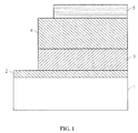
- a light emitting device can have a structure such as shown in FIG. 1 , in which a first electrode 2, a first layer 3 in contact with the electrode 2, a second layer 4 in contact with the layer 3, and a second electrode 5 in contact with the second layer 4.
- First layer 3 can be a hole transporting layer and second layer 4 can be an electron transporting layer. At least one layer can be non-polymelic. Alternatively, a separate emissive layer (not shown in FIG. 1 ) can be included between the hole transporting layer and the electron transporting layer.
- One of the electrodes of the structure is in contact with a substrate 1. Each electrode can contact a power supply to provide a voltage across the structure.
- Electroluminescence can be produced by the emissive layer of the heterostructure when a voltage of proper polarity is applied across the heterostructure.
- First layer 3 can include a plurality of semiconductor nanocrystals, for example, a substantially monodisperse population of nanocrystals.
- a separate emissive layer can include the plurality of nanocrystals.
- a layer that includes nanocrystals can be a monolayer of nanocrystals.
- Light emitting devices including semiconductor nanocrystals can be made by spin-casting a solution containing the HTL organic semiconductor molecules and the semiconductor nanocrystals, where the HTL formed underneath of the semiconductor nanocrystal monolayer via phase separation (see, for example, U.S. Patent Application Nos. 10/400,907 and 10/400,908, both filed March 28, 2003 ).
- This phase separation technique reproducibly placed a monolayer of semiconductor nanocrystals between an organic semiconductor HTL and ETL, thereby effectively exploiting the favorable light emission properties of semiconductor nanocrystals, while minimizing their impact on electrical performance.
- Devices made by this technique were limited by impurities in the solvent, and by the necessity to use organic semiconductor molecules that are soluble in the same solvents as the semiconductor nanocrystals.
- phase separation technique was unsuitable for depositing a monolayer of semiconductor nanocrystals on top of both a HTL and a HIL (due to the solvent destroying the underlying organic thin film). Nor did the phase separation method allow control of the location of semiconductor nanocrystals that emit different colors on the same substrate. Similarly, the phase separation method did not allow patterning of the different color emitting nanocrystals on the same substrate.
- the substrate can be opaque or transparent.
- the substrate can be rigid or flexible.
- the substrate can be plastic, metal or glass.
- the first electrode can be, for example, a high work function hole-injecting conductor, such as an indium tin oxide (ITO) layer.
- ITO indium tin oxide
- Other first electrode materials can include gallium indium tin oxide, zinc indium tin oxide, titanium nitride, or polyaniline.
- the second electrode can be, for example, a low work function (e.g., less than 4.0 eV), electron-injecting, metal, such as Al, Ba, Yb, Ca, a lithium-aluminum alloy (Li:Al), or a magnesium-silver alloy (Mg:Ag).
- the second electrode such as Mg:Ag
- an opaque protective metal layer for example, a layer of Ag for protecting the cathode layer from atmospheric oxidation, or a relatively thin layer of substantially transparent ITO.
- the first electrode can have a thickness of about 500 Angstroms to 4000 Angstroms.
- the first layer can have a thickness of about 50 Angstroms to about 1000 Angstroms.
- the second layer can have a thickness of about 50 Angstroms to about 1000 Angstroms.
- the second electrode can have a thickness of about 50 Angstroms to greater than about 1000 Angstroms.
- the electron transporting layer can be a molecular matrix.
- the molecular matrix can be non-polyxneric.
- the molecular matrix can include a small molecule, for example, a metal complex.
- the metal complex can be a metal complex of 8-hydroxyquinoline.
- the metal complex of 8-hydroxyquinoline can be an aluminum, gallium, indium, zinc or magnesium complex, for example, aluminum tris(8-hydroxyquinoline) (Alq3).
- Other classes of materials in the ETL can include metal thioxinoid compounds, oxadiazole metal chelates, triazoles, sexithiophene derivatives, pyrazine, and styrylanthracene derivatives.
- the hole transporting layer can include an organic chromophore.
- the organic chromophore can be a phenyl amine, such as, for example, N,N'-diphenyl-N,N'-bis(3-methylphenyl)-(1,1'-biphenyl)-4,4'-diamine (TPD).
- TPD N,N'-diphenyl-N,N'-bis(3-methylphenyl)-(1,1'-biphenyl)-4,4'-diamine
- the HTL can include a polyaniline, a polypyrrole, a poly(phenylene vinylene), copper phthalocyanine, an aromatic tertiary amine or polynuclear aromatic tertiary amine, a 4,4'-bis(9-carbazolyl)-1,1'-biphenyl compound, or an N,N,N',N'-tetraarylbenzidine.
- the layers can be deposited on a surface of one of the electrodes by spin coating, dip coating, vapor deposition, or other thin film deposition methods. See, for example, M. C. Schlamp, et al., J. Appl. Phys., 82, 5837-5842, (1997 ); V. Santhanam, et al., Langmuir, 19, 7881-7887, (2003 ); and X. Lin, et al., J. Phys. Chem. B, 105, 3353-3357, (2001 ).
- the second electrode can be sandwiched, sputtered, or evaporated onto the exposed surface of the solid layer. One or both of the electrodes can be patterned.
- the electrodes of the device can be connected to a voltage source by electrically conductive pathways. Upon application of the voltage, light is generated from the device.
- Microcontact printing provides a method for applying a material to a predefined region on a substrate. See, for example, A. Kumar and G. Whitesides, Applied Physics Letters, 63, 2002-2004, (1993 ); and V. Santhanam and R. P. Andres, Nano Latters, 4, 41-44, (2004 ).
- the predefined region is a region on the substrate where the material is selectively applied.
- the material and substrate can be chosen such that the material remains substantially entirely within the predetermined area.
- material can be applied to the substrate such that the material forms a pattern.
- the pattern can be a regular pattern (such as an array, or a series of lines), or an irregular pattern.
- the substrate can have a region including the material (the predefined region) and a region substantially free of material.
- the material forms a monolayer on the substrate.
- the predefined region can be a discontinuous region. In other words, when the material is applied to the predefined region of the substrate, locations including the material can be separated by other locations that are substantially free of the material.
- microcontact printing begins by forming a patterned mold.
- the mold has a surface with a pattern of elevations and depressions.
- a stamp is formed with a complementary pattern of elevations and depressions, for example by coating the patterned surface of the mold with a liquid polymer precursor that is cured while in contact with the patterned mold surface.
- the stamp can then be inked; that is, the stamp is contacted with a material which is to be deposited on a substrate. The material becomes reversibly adhered to the stamp.
- the inked stamp is then contacted with the substrate.
- the elevated regions of the stamp can contact the substrate while the depressed regions of the stamp can be separated from the substrate.
- the ink material (or at least a portion thereof) is transferred from the stamp to the substrate.
- the pattern of elevations and depressions is transferred from the stamp to the substrate as regions including the material and free of the material on the substrate.
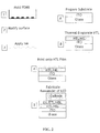
- FIG. 2 depicts a flow chart outlining the basic steps in the microcontact printing process.
- a silicon master is made using standard semiconductor processing techniques which define a pattern on the silicon surface, for example a pattern of elevations and depressions (alternatively, for a non-patterned deposition, a blank Si master can be used).
- Poly dimethyl siloxane (PDMS, for example Sylgard 184) precursors are then mixed, degassed, poured onto the master, and degassed again, and allowed to cure at room temperature (or above room temperature, for faster cure times) (step 1).
- the PDMS stamp having a surface including the pattern of the silicon master, is then freed from the master, and cut into the desired shape and size.
- This stamp can then optionally be modified with a surface chemistry layer, selected to readily adhere and release the ink as needed (step 2).
- the surface chemistry layer can be both a barrier to stamp swelling by the ink solvent, and an adhesion/release layer for the ink.
- Aromatic organic polymers, deposited by chemical vapor deposition, can be used as a surface chemistry layer. See, for example, S. Coe-Sullivan, et al., Advanced Functional Materials, 15, 1117-1124 (2005 ).
- Application of the surface chemistry layer by chemical vapor deposition can result in a conformal coating of the shaped stamp.
- the surface chemistry layer can be chosen to compatible with spreading of chloroform-solvated inks.
- Ink is then applied to the stamp (step 3).
- the inked stamp can then be contacted to a substrate, and gentle pressure applied for 30 seconds to transfer the ink to the new substrate (step 4).
- the ink can include a nanomaterial.
- a nanomaterial can be any material having a dimension smaller than 100 nm.
- the nanomaterial can be, for example, a nanoparticle (e.g., a silica nanoparticle, a titania nanoparticle, or a metal nanoparticle), a semiconductor nanocrystal, a nanotube (such as a single walled or multi-walled carbon nanotube), a nanowire, a nanorod, or a polymer.
- the surface chemistry layer can be a chemical vapor deposited Parylene-C layer.
- the Parylene-C layer can be, for example, 0.1 to 2 ⁇ m thick, depending on the pattern to be reproduced (step 2).
- This stamp is then inked by spin-casting of a solution of semiconductor nanocrystals (step 3).
- the solution can have, for example, a concentration of 1-10 mg/mL of semiconductor nanocrystals dispersed in chloroform. The concentration can be varied depending on desired outcome.
- the inked stamp can then be contacted to a substrate, and gentle pressure applied for 30 seconds to transfer the ink (i.e., a semiconductor nanocrystal monolayer) completely to the new substrate (step 4).
- FIGS. 2A and 2B depict the preparation of an ITO coated glass substrate.
- a hole transport and/or a hole injection layer (HTL and HIL, respectively) including organic semiconductor is thermally evaporated onto the ITO substrate.
- the patterned semiconductor nanocrystal monolayer is transferred to this HTL layer, and the rest of the device (e.g., electron transport layer (ETL), electron injection layer (EIL), and metal contacts) can then be added (step 5).
- ETL electron transport layer
- EIL electron injection layer
- metal contacts metal contacts
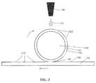
- FIG. 3 depicts a system for forming a pattern of a material on a substrate.
- Liquid applicator 100 delivers ink droplets 110 which form ink spots 120 on printing surface 130 of stamp 135.
- Ink droplets 110 can be applied continuously or intermittently.
- a continuous application can lead to a continuous ink feature on the substrate, whereas intermittent application can result in the formation of an ink pattern on the substrate.
- the nature of the pattern can be controlled by controlling the timing and droplet sizes applied by applicator 100.
- Stamp 135 can be, for example, a cylindrical stamp mounted on the circumference of rotating drum 140.
- Stamp 135 (which can be a textured or featureless stamp) contacts surface 155 of substrate 150 at contact point 160.
- ink spots 120 reach contact point 160, where they are transferred to surface 155 of substrate 150 (moving in the direction indicated by the straight arrow), forming transferred ink spots 170.
- Drum 140 and stamp 135 can be configured to apply pressure to substrate 150 at contact point 160, in order facilitate transfer of ink spots 120.
- the system can be operated continuously.
- Nanocrystals having small diameters can have properties intermediate between molecular and bulk forms of matter. For example, nanocrystals based on semiconductor materials having small diameters can exhibit quantum confinement of both the electron and hole in all three dimensions, which leads to an increase in the effective band gap of the material with decreasing crystallite size. Consequently, both the optical absorption and emission of nanocrystals shift to the blue, or to higher energies, as the size of the crystallites decreases.
- the emission from the nanocrystal can be a narrow Gaussian emission band that can be tuned through the complete wavelength range of the ultraviolet, visible, or infrared regions of the spectrum by varying the size of the nanocrystal, the composition of the nanocrystal, or both.
- CdSe can be tuned in the visible region
- InAs can be tuned in the infrared region.
- the narrow size distribution of a population of nanocrystals can result in emission of light in a narrow spectral range.
- the population can be monodisperse and can exhibit less than a 15% rms deviation in diameter of the nanocrystals, preferably less than 10%, more preferably less than 5%.
- Spectral emissions in a narrow range of no greater than about 75 nm, preferably 60 nm, more preferably 40 nm, and most preferably 30 nm full width at half max (FWHM) can be observed.
- the breadth of the emission decreases as the dispersity of nanocrystal diameters decreases.
- Semiconductor nanocrystals can have high emission quantum efficiencies such as greater than 10%, 20%, 30%, 40%, 50%, 60%, 70%, or 80%.
- the semiconductor forming the nanocrystals can include Group II-VI compounds, Group II-V compounds, Group III-VI compounds, Group III-V compounds, Group IV-VI compounds, Group I-III-VI compounds, Group II-IV-VI compounds, or Group II-IV-V compounds, for example, ZnS, ZnSe, ZnTe, CdS, CdSe, CdTe, HgS, HgSe, HgTe, AlN, AlP, AlAs, AlSb, GaN, GaP, GaAs, GaSb, GaSe, InN, InP, InAs, InSb, TlN, TlP, TlAs, TlSB, PbS, PbSe, PbTe, or mixtures thereof.
- Methods of preparing monodisperse semiconductor nanocrystals include pyrolysis of organometallic reagents, such as dimethyl cadmium, injected into a hot, coordinating solvent. This permits discrete nucleation and results in the controlled growth of macroscopic quantities of nanocrystals. Preparation and manipulation of nanocrystals are described, for example, in U.S. Patent 6,322,901 and 6,576,291 , and U.S. Patent Application No. 60/550,314 .
- the method of manufacturing a nanocrystal is a colloidal growth process. Colloidal growth occurs by rapidly injecting an M donor and an X donor into a hot coordinating solvent.
- the injection produces a nucleus that can be grown in a controlled manner to form a nanocrystal.
- the reaction mixture can be gently heated to grow and anneal the nanocrystal. Both the average size and the size distribution of the nanocrystals in a sample are dependent on the growth temperature. The growth temperature necessary to maintain steady growth increases with increasing average crystal size.
- the nanocrystal is a member of a population of nanocrystals. As a result of the discrete nucleation and controlled growth, the population of nanocrystals obtained has a narrow, monodisperse distribution of diameters. The monodisperse distribution of diameters can also be referred to as a size.
- the process of controlled growth and annealing of the nanocrystals in the coordinating solvent that follows nucleation can also result in uniform surface derivatization and regular core structures. As the size distribution sharpens, the temperature can be raised to maintain steady growth. By adding more M donor or X donor, the growth period can be shortened.
- the M donor can be an inorganic compound, an organometallic compound, or elemental metal.
- M is cadmium, zinc, magnesium, mercury, aluminum, gallium, indium or thallium.
- the X donor is a compound capable of reacting with the M donor to form a material with the general formula MX.
- the X donor is a chalcogenide donor or a pnictide donor, such as a phosphine chalcogenide, a bis(silyl) chalcogenide, dioxygen, an ammonium salt, or a tris(silyl) pnictide.
- Suitable X donors include dioxygen, bis(trimethylsilyl) selenide ((TMS) 2 Se), trialkyl phosphine selenides such as (tri-n-octylphosphine) selenide (TOPSe) or (tri-n-butylphosphine) selenide (TBPSe), trialkyl phosphine tellurides such as (tri-n-octylphosphine) telluride (TOPTe) or hexapropylphosphorustriamide telluride (HPPTTe), bis(trimethylsilyl)telluride ((TMS) 2 Te), bis(trimethylsilyl)sulfide ((TMS) 2 S), a trialkyl phosphine sulfide such as (tri-n-octylphosphine) sulfide (TOPS), an ammonium salt such as an ammonium halide (e.g., NH 4 Cl), tris(trimethyl
- a coordinating solvent can help control the growth of the nanocrystal.
- the coordinating solvent is a compound having a donor lone pair that, for example, has a lone electron pair available to coordinate to a surface of the growing nanocrystal.
- Solvent coordination can stabilize the growing nanocrystal.
- Typical coordinating solvents include alkyl phosphines, alkyl phosphine oxides, alkyl phosphonic acids, or alkyl phosphinic acids, however, other coordinating solvents, such as pyridines, furans, and amines may also be suitable for the nanocrystal production.
- Suitable coordinating solvents include pyridine, tri-n-octyl phosphine (TOP), tri-n-octyl phosphine oxide (TOPO) and tris-hydroxylpropylphosphine (tHPP).
- TOPO tri-n-octyl phosphine
- TOPO tri-n-octyl phosphine oxide
- tHPP tris-hydroxylpropylphosphine
- Size distribution during the growth stage of the reaction can be estimated by monitoring the absorption line widths of the particles. Modification of the reaction temperature in response to changes in the absorption spectrum of the particles allows the maintenance of a sharp particle size distribution during growth. Reactants can be added to the nucleation solution during crystal growth to grow larger crystals. By stopping growth at a particular nanocrystal average diameter and choosing the proper composition of the semiconducting material, the emission spectra of the nanocrystals can be tuned continuously over the wavelength range of 300 nm to 5 microns, or from 400 nm to 800 nm for CdSe and CdTe. The nanocrystal has a diameter of less than 150 ⁇ . A population of nanocrystals has average diameters in the range of 15 ⁇ to 125 ⁇ .
- the nanocrystal can be a member of a population of nanocrystals having a narrow size distribution.
- the nanocrystal can be a sphere, rod, disk, or other shape.
- the nanocrystal can include a core of a semiconductor material.
- the nanocrystal can include a core having the formula MX, where M is cadmium, zinc, magnesium, mercury, aluminum, gallium, indium, thallium, or mixtures thereof, and X is oxygen, sulfur, selenium, tellurium, nitrogen, phosphorus, arsenic, antimony, or mixtures thereof.
- the core can have an overcoating on a surface of the core.
- the overcoating can be a semiconductor material having a composition different from the composition of the core.
- the overcoat of a semiconductor material on a surface of the nanocrystal can include a Group II-VI compounds, Group II-V compounds, Group III-VI compounds, Group III-V compounds, Group IV-VI compounds, Group I-III-VI compounds, Group II-IV-VI compounds, and Group ll-IV-V compounds, for example, ZnS, ZnSe, ZnTe, CdS, CdSe, CdTe, HgS, HgSe, HgTe, AlN, AlP, AlAs, AlSb, GaN, GaP, GaAs, GaSb, GaSe, InN, InP, InAs, InSb, TlN, TlP, TlAs, TISb, PbS, PbSe, PbTe, or mixtures thereof.
- ZnS, ZnSe or CdS overcoatings can be grown on CdSe or CdTe nanocrystals.
- An overcoating process is described, for example, in U.S. Patent 6,322,901 .
- the overcoating can be between 1 and 10 monolayers thick.
- the particle size distribution can be further refined by size selective precipitation with a poor solvent for the nanocrystals, such as methanol/butanol as described in U.S. Patent 6,322,901 .
- a poor solvent for the nanocrystals such as methanol/butanol as described in U.S. Patent 6,322,901 .
- nanocrystals can be dispersed in a solution of 10% butanol in hexane. Methanol can be added dropwise to this stirring solution until opalescence persists. Separation of supernatant and flocculate by centrifugation produces a precipitate enriched with the largest crystallites in the sample. This procedure can be repeated until no further sharpening of the optical absorption spectrum is noted.
- Size-selective precipitation can be carried out in a variety of solvent/nonsolvent pairs, including pyridine/hexane and chloroform/methanol.
- the size-selected nanocrystal population can have no more than a 15% rms deviation from mean diameter, preferably 10% rms deviation or less, and more preferably 5% rms deviation or less.
- the outer surface of the nanocrystal can include a layer of compounds derived from the coordinating solvent used during the growth process.
- the surface can be modified by repeated exposure to an excess of a competing coordinating group to form an overlayer.
- a dispersion of the capped nanocrystal can be treated with a coordinating organic compound, such as pyridine, to produce crystallites which disperse readily in pyridine, methanol, and aromatics but no longer disperse in aliphatic solvents.
- a surface exchange process can be carried out with any compound capable of coordinating to or bonding with the outer surface of the nanocrystal, including, for example, phosphines, thiols, amines and phosphates.
- the nanocrystal can be exposed to short chain polymers which exhibit an affinity for the surface and which terminate in a moiety having an affinity for a suspension or dispersion medium. Such affinity improves the stability of the suspension and discourages flocculation of the nanocrystal.
- Nanocrystal outer layers are described in U.S. Patent 6,251,303 .
- the coordinating ligand can have the formula: wherein k is 2, 3 or 5, and n is 1, 2, 3, 4 or 5 such that k-n is not less than zero;
- each of Y and L independently, is aryl, heteroaryl, or a straight or branched C 2-12 hydrocarbon chain optionally containing at least one double bond, at least one triple bond, or at least one double bond and one triple bond.
- the hydrocarbon chain can be optionally substituted with one or more C 1-4 alkyl, C 2-4 alkenyl, C 2-4 alkynyl, C 1-4 alkoxy, hydroxyl, halo, amino, nitro, cyano, C 3-5 cycloalkyl, 3-5 membered heterocycloalkyl, aryl, heteroaryl, C 1-4 alkylcarbonyloxy, C 1-4 alkyloxycarbonyl, C 1-4 alkylcarbonyl, or formyl.
- the hydrocarbon chain can also be optionally interrupted by -O-, -S-, -N(R a )-, -N(R a )-C(O)-O-, -O-C(O)-N(R a )-, -N(R a )-C(O)-N(R b )-, -O-C(O)-O-, -P(R a )-, or-P(O)(R a )-.
- R a and R b independently, is hydrogen, alkyl, alkenyl, alkynyl, alkoxy, hydroxylalkyl, hydroxyl, or haloalkyl.
- An aryl group is a substituted or unsubstituted cyclic aromatic group. Examples include phenyl, benzyl, naphthyl, tolyl, anthracyl, nitrophenyl, or halophenyl.
- a heteroaryl group is an aryl group with one or more heteroatoms in the ring, for instance furyl, pyiridyl, pyrrolyl, phenanthryl.
- a suitable coordinating ligand can be purchased commercially or prepared by ordinary synthetic organic techniques, for example, as described in J. March, Advanced Organic Chemistry .
- TEM Transmission electron microscopy
- Powder X-ray diffraction (XRD) patterns can provide the most complete information regarding the type and quality of the crystal structure of the nanocrystals.
- Estimates of size are also possible since particle diameter is inversely related, via the X-ray coherence length, to the peak width.
- the diameter of the nanocrystal can be measured directly by transmission electron microscopy or estimated from X-ray diffraction data using, for example, the Scherrer equation. It also can be estimated from the UV/V is absorption spectrum.
- the device can be made in a controlled (oxygen-free and moisture-free) environment, preventing the quenching of luminescent efficiency during the fabrication process.
- Other multilayer structures may be used to improve the device performance (see, for example, U.S. Patent Application Nos. 10/400,908 and 10/400,908 ).
- a blocking layer such as an electron blocking layer (EBL), a hole blocking layer (HBL) or a hole and electron blocking layer (eBL), can be introduced in the structure.
- EBL electron blocking layer
- HBL hole blocking layer
- eBL hole and electron blocking layer
- a blocking layer can include 3-(4-biphenylyl)-4-phenyl-5-tert-butylphenyl-1,2,4-triazole (TAZ), 3,4,5-triphenyl-1,2,4-triazole, 3,5-bis(4-tert-butylphenyl)-4-phenyl-1,2,4-triazole, bathocuproine (BCP), 4,4',4"-tris ⁇ N-(3-methylphenyl)-N-phenylamino ⁇ triphenylamine (m-MTDATA), polyethylene dioxythiophene (PEDOT), 1,3-bis(5-(4-diphenylamino)phenyl-1,3,4-oxadiazol-2-yl)benzene, 2-(4-biphenylyl)-5-(4-tert-butylphenyl)-1,3,4-oxadiazole, 1,3-bis[5-(4-(1,1-dimethylethyl)phenyl)-1,3,
- the performance of organic light emitting devices can be improved by increasing their efficiency, narrowing or broadening their emission spectra, or polarizing their emission. See, for example, Bulovi ⁇ et al., Semiconductors and Semimetals 64, 255 (2000 ), Adachi et al., Appl. Phys. Lett. 78, 1622 (2001 ), Yamasaki et al., Appl. Phys. Lett. 76, 1243 (2000 ), Dirr et al., Jpn. J. Appl. Phys. 37, 1457 (1998 ), and D'Andrade et al., MRS Fall Meeting, BB6.2 (2001). Nanocrystals can be included in efficient hybrid organic/inorganic light emitting devices .
- the narrow FWHM of nanocrystals can result in saturated color emission. This can lead to efficient nanocrystal-light emitting devices even in the red and blue parts of the visible spectrum, since in nanocrystal emitting devices no photons are lost to infrared and UV emission.
- the broadly tunable, saturated color emission over the entire visible spectrum of a single material system is unmatched by any class of organic chromophores (see, for example, Dabbousi et al., J. Phys. Chem. 1.01, 9463 (1997 )).
- a monodisperse population of nanocrystals will emit light spanning a narrow range of wavelengths.
- a device including more than one size of nanocrystal can emit light in more than one narrow range of wavelengths.
- the color of emitted light perceived by a viewer can be controlled by selecting appropriate combinations of nanocrystal sizes and materials in the device.
- environmental stability of covalently bonded inorganic nanocrystals suggests that device lifetimes of hybrid organic/inorganic light emitting devices should match or exceed that of all-organic light emitting devices, when nanocrystals are used as luminescent centers.
- the degeneracy of the band edge energy levels of nanocrystals facilitates capture and radiative recombination of all possible excitons, whether generated by direct charge injection or energy transfer.
- the maximum theoretical nanocrystal-light emitting device efficiencies are therefore comparable to the unity efficiency of phosphorescent organic light emitting devices.
- the excited state lifetime ( ⁇ ) of the nanocrystal is much shorter ( ⁇ ⁇ 10 ns) than a typical phosphor ( ⁇ > 0.5 ⁇ s), enabling nanocrystal-light emitting devices to operate efficiently even at high current density.
- Devices can be prepared that emit visible or infrared light.
- the size and material of a semiconductor nanocrystal can be selected such that the nanocrystal emits visible or infrared light of a selected wavelength.
- the wavelength can be between 300 nm and 2,500 nm or greater, for instance between 300 nm and 400 nm, between 400 nm and 700 nm, between 700 nm and 1100 nm, between 1100 nm and 2500 nm, or greater than 2500 nm.
- the display can include devices that emit at different wavelengths. By patterning the substrate with arrays of different color-emitting semiconductor nanocrystals, a display including pixels of different colors can be formed.
- the substrate can include a backplane.
- the backplane includes active or passive electronics for controlling or switching power to individual pixels. Include a backplane can be useful for applications such as displays, sensors, or imagers.
- the backplane can be configured as an active matrix, passive matrix, fixed format, directly drive, or hybrid.
- the display can be configured for still images, moving images, or lighting.
- a lighting display can provide white light, monochrome light, or color-tunable light.
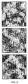
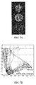
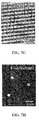
- FIG. 4 demonstrates the surface relief that observed at each step of the microcontact printing process measured by atomic force microscopy (AFM).
- FIG. 4A shows the flatness of the PDMS stamp itself when it was cast onto a planar (non-patterned) master.
- FIGS. 4B and 4C show the stamp inked with semiconductor nanocrystals, and the transferred semiconductor nanocrystals on the organic semiconductor hole transporting layer, respectively.
- the semiconductor nanocrystals formed a sub-monolayer (i.e., a monolayer that does not cover all of the available area) that covered 30-40% of the surface area in FIG. 4C .
- FIGS. 4A shows the flatness of the PDMS stamp itself when it was cast onto a planar (non-patterned) master.
- FIGS. 4B and 4C show the stamp inked with semiconductor nanocrystals, and the transferred semiconductor nanocrystals on the organic semiconductor hole transporting layer, respectively.
- the semiconductor nanocrystals formed a sub-mon
- microcontact printing of semiconductor nanocrystals was a dry process (i.e., does not require solvent) that did not introduce impurities into the device fabrication. All of the organic layers in the device were deposited under ultra-high vacuum conditions. The organic layers were exposed only once to a nitrogen environment for the deposition of the semiconductor nanocrystal layers. None of the organic semiconductor materials were exposed to solvent at any step of the device fabrication.
- HBL hole blocking layer
- TEZ 4-triazole
- Alq 3 tris-(8 hydroxyquinoline)aluminum
- FIG. 5 shows the device characteristics for red, green, and blue light emitting devices fabricated using the semiconductor nanocrystal microcontact printing technique. Red, green, and blue emitting semiconductor nanocrystals were all printed separately onto a thermally evaporated thin film of hole transport material 4-4'-N,N'-dicarbazolyl-biphenyl (CBP).
- CBP hole transport material
- FIGS. 5A-5D presents device characteristics of red, green, and blue emitting light emitting devices.
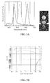
- the electroluminescence (EL) spectra of red-, green-, and blue-emitting devices are shown in FIG. 5A along with digital photos taken of individual red, green, and blue devices.
- the external quantum efficiency and current-voltage curves are presented in FIGS. 5B and 5C , respectively.
- the colors of the lines in each plot correspond to the color of light that the device is emitting.
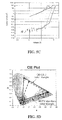
- FIG. 5D shows where those colors being emitted by the respective devices fall on the CIE Chromaticity Diagram relative to the HDTV standard color triangle.
- Color saturation refers to how pure a color appears to the human eye and is quantified in the Commission International d'Eclairage (CIE) chromaticity coordinates, calculated from the emission wavelength and bandwidth (full width at half maximum), which in turn can then be plotted on the CIE diagram as shown in FIG. 5D .
- CIE Commission International d'Eclairage
- the greater color saturation can be attributed to the larger downhill energy transfer process now available with the use of CBP, which results in decreased intensity of organic emission and increased intensity of semiconductor nanocrystal emission, leading in turn to a larger ratio between the semiconductor nanocrystal EL to organic EL.
- the superior color saturation of the red and green semiconductor nanocrystal devices was represented by their position on the CIE diagram relative to the current High Definition Television (HDTV) standard color triangle as seen in FIG. 5D .
- the CIE color coordinates of the blue device lie just inside the HDTV standard color triangle and was a result of the red tail seen in the EL spectrum of the blue device ( FIG. 5A ).
- This red tail can be the result of exiplex emission - in other words, a mixed state between the two large band gap HTL and HBL in our device structure.
- This exiplex emission was not seen in the red device, possibly because those energy states from the exiplex are Förster energy-transferred to the red-emitting semiconductor nanocrystals.
- the green device exhibited only a very small amount of this exiplex emission, probably due to the high degree of film coverage of the monolayer of green emitting semiconductor nanocrystals, which separates the HTL from the HBL and therefore their interaction, as well as the high PL quantum efficiency (40%) of the nanocrystals themselves, which contributes to the large nanocrystal EL intensity relative to the organic exiplex EL.
- Another contributing factor is that when the devices are run at high currents ( ⁇ 100 ⁇ A) the exiplex emission peak shifts from ⁇ 620 nm to ⁇ 520 nm, which is right over the green nanocrystal emission peak and is either covered completely by the green nanocrystal emission or is Förster energy transferred to the green emitting nanocrystals.
- FIG. 5B shows the external quantum efficiency (EQE) of the red, green, and blue semiconductor nanocrystal devices and demonstrates how the EQE of the devices scales with the PL quantum efficiency of the semiconductor nanocrystals.
- EQE external quantum efficiency
- the green-emitting nanocrystal devices had EQEs of 0.5% using semiconductor nanocrystals with PL quantum efficiencies of 40%.
- the blue EQE was 0.25% using semiconductor nanocrystals with PL quantum efficiencies of 20%.
- the semiconductor nanocrystal microcontact printing technique provides the ability to place different color emitting semiconductor nanocrystals on the same substrate in a pattern, leading towards formation of pixels for full color display applications.
- Pixel dimensions for full color displays are typically on the order of 20-30 ⁇ m.
- Patterned semiconductor nanocrystal light emitting devices can be formed on a scale of less than 100 ⁇ m.
- FIG. 6A shows the result of stamping an area of green-emitting semiconductor nanocrystals next to an area of red-emitting semiconductor nanocrystals on the same 1 inch substrate. The three devices that have been turned on in FIG.
- 6A were adjacent red-and green-emitting devices as well as a device on an area where no semiconductor nanocrystals were stamped (i.e, an organic LED with the structure: ITO/CBP/TAZ/Alq 3 /Mg:Ag/Ag).
- FIG. 6B demonstrates the real potential of this technique to achieve sub-100 ⁇ m patterning toward pixelation for nanocrystal light emitting displays.
- green-emitting semiconductor nanocrystals were stamped over the entire area.
- red-emitting semiconductor nanocrystals were stamped down then on top of the green-emitting nanocrystals using a stamp that was patterned with posts.
- the posts were 5 ⁇ m in height and 90 ⁇ m in diameters.
- the device that has been turned on is 0.5 mm in diameter, and the red circles visible within this device are the sub-100 ⁇ m patterned red-emitting semiconductor nanocrystals.
- Microcontact printing can be used to pattern submicron features (see, e.g., U.S. Patent Nos. 5,512,131 ; 6,180,239 ; and 6,518,168 .
- FIG. 6C shows patterned lines of semiconductor nanocrystal monolayers. Such a technique can be employed in the fabrication of full color active matrix nanocrystal light emitting device displays. The stamp was patterned with lines 1 ⁇ m high and 100 ⁇ m in width.
- FIG. 7A The printed nanocrystal monolayers generated electroluminescence in the red, green, and blue devices pictured in FIG. 7A , which all have the same layered thin film structure: ITO/CBP (40 nm thick layer)/nanocrystal monolayer/ TAZ (15 nm)/Alq 3 (25 nm)/Mg:Ag/Ag (see FIG. 7D inset).
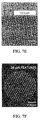
- FIG. 7C is an AFM image of a nanocrystal monolayer after it has been stamped onto the organic hole transporting layer.
- the only difference between the devices pictured in FIG. 7A is the luminescence color of the nanocrystal monolayer, determined by the size and composition of the nanocrystals. All the organic and metal films were thermally evaporated at 10 -6 Torr.
- FIGS. 7F and 7G show that 25 ⁇ m (1000 dpi) patterning of LED pixels was achieved, as were 150 nm wide nanocrystal monolayer patterns ( FIG. 7E ).
- 25 ⁇ m wide intersecting stripes of red and green nanocrystal monolayers were stamped over each other in the LED structure in which TPD (40 nm thick) replaced CBP.
- FIG. 7H is a photograph of operating nanocrystal LEDs demonstrating multicolor area patterning with micro-contact printing. Two adjacent areas on the same substrate were stamped with a monolayer of red and green emitting nanocrystals.
- the solvent-free deposition of the nanocrystal monolayers enabled use of the thermally evaporated organic semiconductor, CBP, as a hole transport layer.
- CBP thermally evaporated organic semiconductor
- the wide band gap of CBP contributed to more efficient charge confinement and an improvement in color saturation of the LEDs, yielding CIE coordinates (0.18, 0.13), (0.21, 0.70), and (0.66, 0.34) for the blue, green, and red LED, respectively, and with corresponding external quantum efficiencies of 0.2%, 0.5%, and 1.0% at video brightness ( FIG. 7B ).
- Current/voltage data for the three different colors are presented in FIG. 7D .
- the wide range of colors produced by nanocrystal-LEDs exceeded the performance of both liquid crystal display (LCD) and organic LED (OLED) technologies, suggesting the suitability of nanocrystal based LEDs in high definition, accurate color flat panel displays and in general light sources.
- Red-, green-, and blue-emitting semiconductor nanocrystal-based light emitting devices are efficient, highly color saturated compared to organic LEDs and liquid crystal displays, and can be patterned towards pixelation for full color display applications by means of microcontact printing of single layers of nanocrystals.
Landscapes
- Engineering & Computer Science (AREA)
- Chemical & Material Sciences (AREA)
- Nanotechnology (AREA)
- Manufacturing & Machinery (AREA)
- Physics & Mathematics (AREA)
- Crystallography & Structural Chemistry (AREA)
- General Engineering & Computer Science (AREA)
- Optics & Photonics (AREA)
- Composite Materials (AREA)
- Biophysics (AREA)
- Life Sciences & Earth Sciences (AREA)
- Condensed Matter Physics & Semiconductors (AREA)
- General Physics & Mathematics (AREA)
- Materials Engineering (AREA)
- Electroluminescent Light Sources (AREA)
- Application Of Or Painting With Fluid Materials (AREA)
- Exposure Of Semiconductors, Excluding Electron Or Ion Beam Exposure (AREA)
- Thin Film Transistor (AREA)
- Manufacturing Of Printed Wiring (AREA)
- Electrodes Of Semiconductors (AREA)
- Led Devices (AREA)
- Led Device Packages (AREA)
Applications Claiming Priority (3)
| Application Number | Priority Date | Filing Date | Title |
|---|---|---|---|
| US62096704P | 2004-10-22 | 2004-10-22 | |
| US62957904P | 2004-11-22 | 2004-11-22 | |
| EP05857963A EP1803174B1 (en) | 2004-10-22 | 2005-10-21 | Method of forming a light emitting device including semiconductor nanocrystals |
Related Parent Applications (2)
| Application Number | Title | Priority Date | Filing Date |
|---|---|---|---|
| EP05857963.2 Division | 2005-10-21 | ||
| EP05857963A Division EP1803174B1 (en) | 2004-10-22 | 2005-10-21 | Method of forming a light emitting device including semiconductor nanocrystals |
Related Child Applications (2)
| Application Number | Title | Priority Date | Filing Date |
|---|---|---|---|
| EP10185494 Division-Into | 2010-10-01 | ||
| EP10185494.1 Division-Into | 2010-10-01 |
Publications (2)
| Publication Number | Publication Date |
|---|---|
| EP2254393A1 EP2254393A1 (en) | 2010-11-24 |
| EP2254393B1 true EP2254393B1 (en) | 2016-05-11 |
Family
ID=36118185
Family Applications (4)
| Application Number | Title | Priority Date | Filing Date |
|---|---|---|---|
| EP10164996.0A Expired - Lifetime EP2254393B1 (en) | 2004-10-22 | 2005-10-21 | Light emitting device including semiconductor nanocrystals |
| EP05857963A Expired - Lifetime EP1803174B1 (en) | 2004-10-22 | 2005-10-21 | Method of forming a light emitting device including semiconductor nanocrystals |
| EP12165772.0A Expired - Lifetime EP2498274B1 (en) | 2004-10-22 | 2005-10-21 | Method for transferring a patterned material |
| EP05810107.2A Expired - Lifetime EP1807863B1 (en) | 2004-10-22 | 2005-10-21 | Method for transferring a patterned material |
Family Applications After (3)
| Application Number | Title | Priority Date | Filing Date |
|---|---|---|---|
| EP05857963A Expired - Lifetime EP1803174B1 (en) | 2004-10-22 | 2005-10-21 | Method of forming a light emitting device including semiconductor nanocrystals |
| EP12165772.0A Expired - Lifetime EP2498274B1 (en) | 2004-10-22 | 2005-10-21 | Method for transferring a patterned material |
| EP05810107.2A Expired - Lifetime EP1807863B1 (en) | 2004-10-22 | 2005-10-21 | Method for transferring a patterned material |
Country Status (8)
| Country | Link |
|---|---|
| US (2) | US10225906B2 (enExample) |
| EP (4) | EP2254393B1 (enExample) |
| JP (4) | JP2008518401A (enExample) |
| KR (3) | KR101369205B1 (enExample) |
| AT (1) | ATE470959T1 (enExample) |
| DE (1) | DE602005021808D1 (enExample) |
| TW (2) | TWI440205B (enExample) |
| WO (2) | WO2006047215A2 (enExample) |
Families Citing this family (102)
| Publication number | Priority date | Publication date | Assignee | Title |
|---|---|---|---|---|
| US10225906B2 (en) * | 2004-10-22 | 2019-03-05 | Massachusetts Institute Of Technology | Light emitting device including semiconductor nanocrystals |
| US7799422B2 (en) * | 2004-11-03 | 2010-09-21 | Massachusetts Institute Of Technology | Absorbing film |
| US7649196B2 (en) | 2004-11-03 | 2010-01-19 | Massachusetts Institute Of Technology | Light emitting device |
| US8891575B2 (en) * | 2004-11-30 | 2014-11-18 | Massachusetts Institute Of Technology | Optical feedback structures and methods of making |
| US20070153362A1 (en) * | 2004-12-27 | 2007-07-05 | Regents Of The University Of California | Fabric having nanostructured thin-film networks |
| US8232722B2 (en) | 2005-02-16 | 2012-07-31 | Massachusetts Institute Of Technology | Light emitting devices including semiconductor nanocrystals |
| US8845927B2 (en) * | 2006-06-02 | 2014-09-30 | Qd Vision, Inc. | Functionalized nanoparticles and method |
| US8718437B2 (en) | 2006-03-07 | 2014-05-06 | Qd Vision, Inc. | Compositions, optical component, system including an optical component, devices, and other products |
| WO2007103310A2 (en) | 2006-03-07 | 2007-09-13 | Qd Vision, Inc. | An article including semiconductor nanocrystals |
| US9297092B2 (en) * | 2005-06-05 | 2016-03-29 | Qd Vision, Inc. | Compositions, optical component, system including an optical component, devices, and other products |
| US20080023067A1 (en) * | 2005-12-27 | 2008-01-31 | Liangbing Hu | Solar cell with nanostructure electrode |
| US20070236138A1 (en) * | 2005-12-27 | 2007-10-11 | Liangbing Hu | Organic light-emitting diodes with nanostructure film electrode(s) |
| US8138075B1 (en) | 2006-02-06 | 2012-03-20 | Eberlein Dietmar C | Systems and methods for the manufacture of flat panel devices |
| JP2009526370A (ja) * | 2006-02-09 | 2009-07-16 | キユーデイー・ビジヨン・インコーポレーテツド | 半導体ナノ結晶およびドープされた有機材料を含む層を含むデバイスおよび方法 |
| US8835941B2 (en) * | 2006-02-09 | 2014-09-16 | Qd Vision, Inc. | Displays including semiconductor nanocrystals and methods of making same |
| EP1989725B1 (en) | 2006-02-14 | 2019-06-05 | Massachusetts Institute of Technology | White light emitting devices |
| WO2007143197A2 (en) | 2006-06-02 | 2007-12-13 | Qd Vision, Inc. | Light-emitting devices and displays with improved performance |
| US8849087B2 (en) | 2006-03-07 | 2014-09-30 | Qd Vision, Inc. | Compositions, optical component, system including an optical component, devices, and other products |
| US9874674B2 (en) | 2006-03-07 | 2018-01-23 | Samsung Electronics Co., Ltd. | Compositions, optical component, system including an optical component, devices, and other products |
| US9951438B2 (en) | 2006-03-07 | 2018-04-24 | Samsung Electronics Co., Ltd. | Compositions, optical component, system including an optical component, devices, and other products |
| WO2008070028A2 (en) * | 2006-12-01 | 2008-06-12 | Qd Vision, Inc. | Improved composites and devices including nanoparticles |
| WO2007112088A2 (en) * | 2006-03-24 | 2007-10-04 | Qd Vision, Inc. | Hyperspectral imaging device |
| WO2007117698A2 (en) * | 2006-04-07 | 2007-10-18 | Qd Vision, Inc. | Composition including material, methods of depositing material, articles including same and systems for depositing material |
| WO2007120877A2 (en) * | 2006-04-14 | 2007-10-25 | Qd Vision, Inc. | Transfer surface for manufacturing a light emitting device |
| US8941299B2 (en) * | 2006-05-21 | 2015-01-27 | Massachusetts Institute Of Technology | Light emitting device including semiconductor nanocrystals |
| US9212056B2 (en) * | 2006-06-02 | 2015-12-15 | Qd Vision, Inc. | Nanoparticle including multi-functional ligand and method |
| WO2007143227A2 (en) * | 2006-06-10 | 2007-12-13 | Qd Vision, Inc. | Materials,thin films,optical filters, and devices including same |
| WO2008111947A1 (en) | 2006-06-24 | 2008-09-18 | Qd Vision, Inc. | Methods and articles including nanomaterial |
| WO2008105792A2 (en) | 2006-06-24 | 2008-09-04 | Qd Vision, Inc. | Methods for depositing nanomaterial, methods for fabricating a device, methods for fabricating an array of devices and compositions |
| WO2008108798A2 (en) | 2006-06-24 | 2008-09-12 | Qd Vision, Inc. | Methods for depositing nanomaterial, methods for fabricating a device, and methods for fabricating an array of devices |
| US8643058B2 (en) | 2006-07-31 | 2014-02-04 | Massachusetts Institute Of Technology | Electro-optical device including nanocrystals |
| US8084101B2 (en) * | 2006-08-01 | 2011-12-27 | The Board of Regents of the Nevada Systems of Higher Education on behalf of the University of Nevada, Las Vegas | Fabrication of patterned and ordered nanoparticles |
| US20080047930A1 (en) * | 2006-08-23 | 2008-02-28 | Graciela Beatriz Blanchet | Method to form a pattern of functional material on a substrate |
| JP2010508620A (ja) * | 2006-09-12 | 2010-03-18 | キユーデイー・ビジヨン・インコーポレーテツド | 所定のパターンを表示するために有用なエレクトロルミネセントディスプレイ |
| WO2008033388A2 (en) * | 2006-09-12 | 2008-03-20 | Qd Vision, Inc. | A composite including nanoparticles, methods, and products including a composite |
| US8219170B2 (en) * | 2006-09-20 | 2012-07-10 | Nellcor Puritan Bennett Llc | System and method for practicing spectrophotometry using light emitting nanostructure devices |
| US20080083484A1 (en) * | 2006-09-28 | 2008-04-10 | Graciela Beatriz Blanchet | Method to form a pattern of functional material on a substrate |
| US20080110363A1 (en) * | 2006-11-14 | 2008-05-15 | National Chung Cheng University | Physisorption-based microcontact printing process capable of controlling film thickness |
| WO2008063652A1 (en) | 2006-11-21 | 2008-05-29 | Qd Vision, Inc. | Blue emitting semiconductor nanocrystals and compositions and devices including same |
| WO2008133660A2 (en) * | 2006-11-21 | 2008-11-06 | Qd Vision, Inc. | Nanocrystals including a group iiia element and a group va element, method, composition, device and other prodcucts |
| WO2008063653A1 (en) | 2006-11-21 | 2008-05-29 | Qd Vision, Inc. | Semiconductor nanocrystals and compositions and devices including same |
| WO2008063658A2 (en) | 2006-11-21 | 2008-05-29 | Qd Vision, Inc. | Semiconductor nanocrystals and compositions and devices including same |
| WO2008063657A2 (en) * | 2006-11-21 | 2008-05-29 | Qd Vision, Inc. | Light emitting devices and displays with improved performance |
| KR100850717B1 (ko) * | 2006-12-06 | 2008-08-06 | 삼성전자주식회사 | 이미지형성체와 그 제조장치 및 방법 |
| KR101391807B1 (ko) * | 2007-01-03 | 2014-05-08 | 삼성디스플레이 주식회사 | 잉크젯 프린팅과 나노 임프린팅을 이용한 패턴 형성 방법 |
| US8836212B2 (en) * | 2007-01-11 | 2014-09-16 | Qd Vision, Inc. | Light emissive printed article printed with quantum dot ink |
| US20080172197A1 (en) * | 2007-01-11 | 2008-07-17 | Motorola, Inc. | Single laser multi-color projection display with quantum dot screen |
| US20080233489A1 (en) * | 2007-03-22 | 2008-09-25 | Graciela Beatriz Blanchet | Method to form a pattern of functional material on a substrate using a stamp having a surface modifying material |
| US8222061B2 (en) * | 2007-03-30 | 2012-07-17 | The Penn State Research Foundation | Mist fabrication of quantum dot devices |
| US7875313B2 (en) | 2007-04-05 | 2011-01-25 | E. I. Du Pont De Nemours And Company | Method to form a pattern of functional material on a substrate using a mask material |
| JP5773646B2 (ja) | 2007-06-25 | 2015-09-02 | キユーデイー・ビジヨン・インコーポレーテツド | ナノ材料を被着させることを含む組成物および方法 |
| US10043993B2 (en) * | 2007-06-25 | 2018-08-07 | Massachusetts Institute Of Technology | Electro-optical device |
| WO2009002551A1 (en) * | 2007-06-26 | 2008-12-31 | Qd Vision, Inc. | Photovoltaic devices including quantum dot down-conversion materials useful for solar cells and materials including quantum dots |
| US7989153B2 (en) * | 2007-07-11 | 2011-08-02 | Qd Vision, Inc. | Method and apparatus for selectively patterning free standing quantum DOT (FSQDT) polymer composites |
| WO2009014707A2 (en) | 2007-07-23 | 2009-01-29 | Qd Vision, Inc. | Quantum dot light enhancement substrate and lighting device including same |
| US20110079273A1 (en) * | 2008-01-10 | 2011-04-07 | Massachusetts Institute Of Technology | Photovoltaic devices |
| US8525022B2 (en) * | 2008-01-11 | 2013-09-03 | Massachusetts Institute Of Technology | High efficiency multi-layer photovoltaic devices |
| WO2009099425A2 (en) * | 2008-02-07 | 2009-08-13 | Qd Vision, Inc. | Flexible devices including semiconductor nanocrystals, arrays, and methods |
| CN105870345B (zh) | 2008-04-03 | 2019-01-01 | 三星研究美国股份有限公司 | 包括量子点的发光器件 |
| US9525148B2 (en) | 2008-04-03 | 2016-12-20 | Qd Vision, Inc. | Device including quantum dots |
| US9207385B2 (en) | 2008-05-06 | 2015-12-08 | Qd Vision, Inc. | Lighting systems and devices including same |
| WO2009137053A1 (en) | 2008-05-06 | 2009-11-12 | Qd Vision, Inc. | Optical components, systems including an optical component, and devices |
| JP2011524064A (ja) | 2008-05-06 | 2011-08-25 | キユーデイー・ビジヨン・インコーポレーテツド | 量子閉じ込め半導体ナノ粒子を含有する固体照明装置 |
| US8765223B2 (en) * | 2008-05-08 | 2014-07-01 | Air Products And Chemicals, Inc. | Binary and ternary metal chalcogenide materials and method of making and using same |
| US8507040B2 (en) | 2008-05-08 | 2013-08-13 | Air Products And Chemicals, Inc. | Binary and ternary metal chalcogenide materials and method of making and using same |
| US8269985B2 (en) * | 2009-05-26 | 2012-09-18 | Zena Technologies, Inc. | Determination of optimal diameters for nanowires |
| US20100330367A1 (en) * | 2009-02-03 | 2010-12-30 | Ut-Battelle, Llc | Microbially-mediated method for synthesis of non-oxide semiconductor nanoparticles |
| KR101753740B1 (ko) | 2009-04-28 | 2017-07-04 | 삼성전자주식회사 | 광학 재료, 광학 부품 및 방법 |
| WO2010129887A2 (en) | 2009-05-07 | 2010-11-11 | Massachusetts Institute Of Technology | Light emitting device including semiconductor nanocrystals |
| WO2010129889A2 (en) | 2009-05-07 | 2010-11-11 | Massachusetts Institute Of Technology | Light emitting device including semiconductor nanocrystals |
| US8106420B2 (en) | 2009-06-05 | 2012-01-31 | Massachusetts Institute Of Technology | Light emitting device including semiconductor nanocrystals |
| US9340697B2 (en) * | 2009-08-14 | 2016-05-17 | Nano-C, Inc. | Solvent-based and water-based carbon nanotube inks with removable additives |
| KR20120062773A (ko) | 2009-08-14 | 2012-06-14 | 큐디 비젼, 인크. | 조명 장치, 조명 장치용 광학 요소, 및 방법 |
| KR101865888B1 (ko) | 2009-09-09 | 2018-06-08 | 삼성전자주식회사 | 나노입자들을 포함하는 입자, 그의 용도, 및 방법 |
| WO2011031876A1 (en) | 2009-09-09 | 2011-03-17 | Qd Vision, Inc. | Formulations including nanoparticles |
| JP2013508895A (ja) | 2009-10-17 | 2013-03-07 | キユーデイー・ビジヨン・インコーポレーテツド | 光学部品、これを含む製品およびこれを作製する方法 |
| KR101924080B1 (ko) | 2009-11-11 | 2018-11-30 | 삼성 리서치 아메리카 인코포레이티드 | 양자점을 포함하는 디바이스 |
| EP2553714B1 (en) * | 2010-04-02 | 2016-08-31 | Rhodia Operations | Methods for transferring nanoparticles onto substrates and for patterning nanoparticle films. |
| TW201225370A (en) * | 2010-12-15 | 2012-06-16 | Nat Univ Tsing Hua | Method for manufacturing high-quality organic light-emitting diode (OLED) |
| WO2012134629A1 (en) | 2011-04-01 | 2012-10-04 | Qd Vision, Inc. | Quantum dots, method, and devices |
| WO2013019299A2 (en) | 2011-05-11 | 2013-02-07 | Qd Vision, Inc. | Method for processing devices including quantum dots and devices |
| WO2012158832A2 (en) | 2011-05-16 | 2012-11-22 | Qd Vision, Inc. | Method for preparing semiconductor nanocrystals |
| US9520573B2 (en) | 2011-05-16 | 2016-12-13 | Qd Vision, Inc. | Device including quantum dots and method for making same |
| WO2013028253A1 (en) | 2011-08-19 | 2013-02-28 | Qd Vision, Inc. | Semiconductor nanocrystals and methods |
| DE112011105527B4 (de) * | 2011-09-21 | 2020-01-16 | Ev Group E. Thallner Gmbh | Verfahren zur Herstellung einer polychromatisierenden Schicht und Substrat sowie Leuchtdiode mit polychromatisierender Schicht |
| JP2013138179A (ja) * | 2011-11-30 | 2013-07-11 | Central Glass Co Ltd | 光重合性組成物並びにそれを用いたパターン形成方法 |
| WO2013103440A1 (en) | 2012-01-06 | 2013-07-11 | Qd Vision, Inc. | Light emitting device including blue emitting quantum dots and method |
| US9929325B2 (en) | 2012-06-05 | 2018-03-27 | Samsung Electronics Co., Ltd. | Lighting device including quantum dots |
| WO2014088667A2 (en) | 2012-09-14 | 2014-06-12 | Qd Vision, Inc. | Light emitting device including tandem structure |
| KR101429118B1 (ko) * | 2013-02-04 | 2014-08-14 | 한국과학기술연구원 | 자기조립 나노 구조물을 이용한 반사 방지막 및 그 제조방법 |
| US9574135B2 (en) * | 2013-08-22 | 2017-02-21 | Nanoco Technologies Ltd. | Gas phase enhancement of emission color quality in solid state LEDs |
| US20160365478A1 (en) | 2013-12-27 | 2016-12-15 | The Board Of Trustee Of The University Of Illinois | Nanostructure material stack-transfer methods and devices |
| KR101651872B1 (ko) * | 2015-04-23 | 2016-08-29 | 경북대학교 산학협력단 | 나노 결정 발광 다이오드 및 그 제조 방법 |
| CN108400251B (zh) * | 2018-04-23 | 2024-09-10 | 华南理工大学 | 一种高分辨率的钙钛矿电致发光器件及其制备方法 |
| US11152536B2 (en) | 2018-09-17 | 2021-10-19 | The Board Of Trustees Of The University Of Illinois | Photoresist contact patterning of quantum dot films |
| CN109301093B (zh) * | 2018-09-30 | 2024-06-07 | 华南理工大学 | 一种导电可透光钙钛矿量子点薄膜的制备方法 |
| KR102806941B1 (ko) * | 2019-10-23 | 2025-05-12 | 엘지디스플레이 주식회사 | 무기발광다이오드 및 무기발광장치 |
| JP7416929B2 (ja) * | 2019-10-28 | 2024-01-17 | フラウンホーファー-ゲゼルシャフト ツア フォルデルング デア アンゲヴァンテン フォルシュング エー ファウ | 偏光発光を有する発光ダイオードの製造方法 |
| IT201900020138A1 (it) * | 2019-10-31 | 2021-05-01 | Fabio Fontana | Dispositivo terapeutico per patologia infiammatoria, dolorosa e una rimodulazione neuro-muscolare e posturale |
| US12105417B2 (en) | 2021-10-05 | 2024-10-01 | Canon Kabushiki Kaisha | Method of forming a photo-cured layer |
| FR3149999B1 (fr) * | 2023-06-16 | 2025-06-13 | Aeroprotec Services | Procede de marquage 3d |
| EP4523918A1 (en) * | 2023-09-12 | 2025-03-19 | FononTech Holding B.V. | Deposition method and device |
Family Cites Families (108)
| Publication number | Priority date | Publication date | Assignee | Title |
|---|---|---|---|---|
| US550314A (en) | 1895-11-26 | Combined ferrule and bushing | ||
| US400908A (en) | 1889-04-09 | Gustav fuchs | ||
| US3998573A (en) * | 1972-01-17 | 1976-12-21 | Abex Corporation | Manufacture of friction elements |
| DE3830775A1 (de) * | 1987-09-11 | 1989-03-23 | Ricoh Kk | Thermisches mimeograph-schablonenpapier |
| KR920007701A (ko) * | 1990-10-05 | 1992-05-27 | 이시다 아키라 | 균일한 두께의 박막을 형성하기 위한 롤 코팅장치 |
| US5099256A (en) * | 1990-11-23 | 1992-03-24 | Xerox Corporation | Ink jet printer with intermediate drum |
| JP3125332B2 (ja) * | 1991-06-21 | 2001-01-15 | ソニー株式会社 | 量子ドットトンネル素子とそれを用いた情報処理装置及び情報処理方法 |
| JPH05116475A (ja) | 1991-10-29 | 1993-05-14 | Kimoto & Co Ltd | 表面改質孔版およびその表面改質方法 |
| EP0613585A4 (en) | 1991-11-22 | 1995-06-21 | Univ California | SEMICONDUCTING NANOCRYSTALS CONNECTED TO SOLID INORGANIC SURFACES BY SELF-ASSEMBLED SINGLE LAYERS. |
| US5505928A (en) | 1991-11-22 | 1996-04-09 | The Regents Of University Of California | Preparation of III-V semiconductor nanocrystals |
| US5260957A (en) * | 1992-10-29 | 1993-11-09 | The Charles Stark Draper Laboratory, Inc. | Quantum dot Laser |
| US5293050A (en) | 1993-03-25 | 1994-03-08 | International Business Machines Corporation | Semiconductor quantum dot light emitting/detecting devices |
| US6048616A (en) | 1993-04-21 | 2000-04-11 | Philips Electronics N.A. Corp. | Encapsulated quantum sized doped semiconductor particles and method of manufacturing same |
| US6180239B1 (en) | 1993-10-04 | 2001-01-30 | President And Fellows Of Harvard College | Microcontact printing on surfaces and derivative articles |
| US5512131A (en) * | 1993-10-04 | 1996-04-30 | President And Fellows Of Harvard College | Formation of microstamped patterns on surfaces and derivative articles |
| US5900160A (en) | 1993-10-04 | 1999-05-04 | President And Fellows Of Harvard College | Methods of etching articles via microcontact printing |
| US5422489A (en) | 1994-01-24 | 1995-06-06 | Bhargava; Rameshwar N. | Light emitting device |
| US5537000A (en) | 1994-04-29 | 1996-07-16 | The Regents, University Of California | Electroluminescent devices formed using semiconductor nanocrystals as an electron transport media and method of making such electroluminescent devices |
| JPH0834116A (ja) * | 1994-07-22 | 1996-02-06 | Fuji Xerox Co Ltd | インクジェット記録装置 |
| US5677545A (en) | 1994-09-12 | 1997-10-14 | Motorola | Organic light emitting diodes with molecular alignment and method of fabrication |
| CA2199506C (en) | 1994-09-29 | 2001-07-31 | Michael Graham Burt | Optical fibre with quantum dots |
| FR2726185B1 (fr) * | 1994-11-02 | 1997-04-25 | Oreal | Composition tinctoriale a base de colorants d'oxydation et procede de teinture mettant en oeuvre cette composition |
| US5585640A (en) * | 1995-01-11 | 1996-12-17 | Huston; Alan L. | Glass matrix doped with activated luminescent nanocrystalline particles |
| US6518168B1 (en) | 1995-08-18 | 2003-02-11 | President And Fellows Of Harvard College | Self-assembled monolayer directed patterning of surfaces |
| GB9518910D0 (en) | 1995-09-15 | 1995-11-15 | Imperial College | Process |
| US5853446A (en) * | 1996-04-16 | 1998-12-29 | Corning Incorporated | Method for forming glass rib structures |
| KR100457148B1 (ko) * | 1996-10-10 | 2004-11-16 | 알제이알폴리머스,인코포레이티드 | 역 스탬핑 방법 |
| US6103868A (en) * | 1996-12-27 | 2000-08-15 | The Regents Of The University Of California | Organically-functionalized monodisperse nanocrystals of metals |
| US5958573A (en) | 1997-02-10 | 1999-09-28 | Quantum Energy Technologies | Electroluminescent device having a structured particle electron conductor |
| JP4071360B2 (ja) | 1997-08-29 | 2008-04-02 | 株式会社東芝 | 半導体装置 |
| JPH11135838A (ja) | 1997-10-20 | 1999-05-21 | Ind Technol Res Inst | 白色発光ダイオード及びその製造方法 |
| US6322901B1 (en) | 1997-11-13 | 2001-11-27 | Massachusetts Institute Of Technology | Highly luminescent color-selective nano-crystalline materials |
| US6607829B1 (en) | 1997-11-13 | 2003-08-19 | Massachusetts Institute Of Technology | Tellurium-containing nanocrystalline materials |
| US6236060B1 (en) * | 1997-11-19 | 2001-05-22 | International Business Machines Corporation | Light emitting structures in back-end of line silicon technology |
| DE19812258A1 (de) * | 1998-03-20 | 1999-09-23 | Bayer Ag | Elektrolumineszierende Anordnungen unter Verwendung von Blendsystemen |
| JPH11273859A (ja) * | 1998-03-24 | 1999-10-08 | Sony Corp | 有機電界発光素子及びその製造方法 |
| US6501091B1 (en) | 1998-04-01 | 2002-12-31 | Massachusetts Institute Of Technology | Quantum dot white and colored light emitting diodes |
| JP4126751B2 (ja) | 1998-05-26 | 2008-07-30 | ソニー株式会社 | 表示装置および照明装置 |
| US6864626B1 (en) * | 1998-06-03 | 2005-03-08 | The Regents Of The University Of California | Electronic displays using optically pumped luminescent semiconductor nanocrystals |
| AU5199699A (en) | 1998-07-29 | 2000-02-21 | W.A. Sanders Papierfabriek 'coldenhove' B.V. | Transfer paper for ink-jet printing |
| US6294401B1 (en) | 1998-08-19 | 2001-09-25 | Massachusetts Institute Of Technology | Nanoparticle-based electrical, chemical, and mechanical structures and methods of making same |
| US6251303B1 (en) * | 1998-09-18 | 2001-06-26 | Massachusetts Institute Of Technology | Water-soluble fluorescent nanocrystals |
| US6617583B1 (en) * | 1998-09-18 | 2003-09-09 | Massachusetts Institute Of Technology | Inventory control |
| WO2000017903A2 (en) * | 1998-09-22 | 2000-03-30 | Fed Corporation | Inorganic-based color conversion matrix element for organic color display devices and method of fabrication |
| JP2000104058A (ja) | 1998-09-28 | 2000-04-11 | Sony Corp | 発光体の製造方法 |
| US6506438B2 (en) * | 1998-12-15 | 2003-01-14 | E Ink Corporation | Method for printing of transistor arrays on plastic substrates |
| JP3988309B2 (ja) * | 1999-01-14 | 2007-10-10 | ソニー株式会社 | 蛍光体及びその製造方法 |
| US6348295B1 (en) * | 1999-03-26 | 2002-02-19 | Massachusetts Institute Of Technology | Methods for manufacturing electronic and electromechanical elements and devices by thin-film deposition and imaging |
| JP4877675B2 (ja) * | 1999-06-28 | 2012-02-15 | 株式会社半導体エネルギー研究所 | 電気光学装置の作製方法 |
| TW556357B (en) | 1999-06-28 | 2003-10-01 | Semiconductor Energy Lab | Method of manufacturing an electro-optical device |
| US6249104B1 (en) * | 1999-07-01 | 2001-06-19 | General Electric Company | Cutout start switch heating |
| JP2001113772A (ja) * | 1999-08-11 | 2001-04-24 | Canon Inc | 画像形成装置 |
| JP2001274528A (ja) * | 2000-01-21 | 2001-10-05 | Fujitsu Ltd | 薄膜デバイスの基板間転写方法 |
| US6797412B1 (en) | 2000-04-11 | 2004-09-28 | University Of Connecticut | Full color display structures using pseudomorphic cladded quantum dot nanophosphor thin films |
| US6380101B1 (en) * | 2000-04-18 | 2002-04-30 | International Business Machines Corporation | Method of forming patterned indium zinc oxide and indium tin oxide films via microcontact printing and uses thereof |
| US7491286B2 (en) * | 2000-04-21 | 2009-02-17 | International Business Machines Corporation | Patterning solution deposited thin films with self-assembled monolayers |
| US6887332B1 (en) * | 2000-04-21 | 2005-05-03 | International Business Machines Corporation | Patterning solution deposited thin films with self-assembled monolayers |
| US7323143B2 (en) * | 2000-05-25 | 2008-01-29 | President And Fellows Of Harvard College | Microfluidic systems including three-dimensionally arrayed channel networks |
| AU2001289859A1 (en) * | 2000-09-05 | 2002-03-22 | Zeptosens Ag | Method for precipitating mono and multiple layers of organophosphoric and organophosphonic acids and the salts thereof in addition to use thereof |
| US6576291B2 (en) * | 2000-12-08 | 2003-06-10 | Massachusetts Institute Of Technology | Preparation of nanocrystallites |
| JP2002192540A (ja) * | 2000-12-22 | 2002-07-10 | Mitsubishi Rayon Co Ltd | 転写ロールおよびその加工方法、それを用いた光学シートの製造方法 |
| EP1386523A1 (en) | 2001-05-09 | 2004-02-04 | Gakoreatech | Manufacturing process of self-luminous and flexible fabric |
| US6896872B2 (en) | 2001-06-27 | 2005-05-24 | Svetlana A. Dambinova | Rapid multiple panel of biomarkers in laboratory blood tests for TIA/stroke |
| US6846565B2 (en) | 2001-07-02 | 2005-01-25 | Board Of Regents, The University Of Texas System | Light-emitting nanoparticles and method of making same |
| EP1425355A1 (en) * | 2001-07-12 | 2004-06-09 | Eastman Kodak Company | A compressed fluid formulation |
| WO2003092043A2 (en) * | 2001-07-20 | 2003-11-06 | Quantum Dot Corporation | Luminescent nanoparticles and methods for their preparation |
| JP5055672B2 (ja) | 2001-07-31 | 2012-10-24 | 大日本印刷株式会社 | 薄膜パターン形成用スタンプ |
| JP4340405B2 (ja) * | 2001-08-09 | 2009-10-07 | 富士フイルム株式会社 | 有機el素子の製造方法及び有機el素子 |
| JP2005502176A (ja) * | 2001-09-04 | 2005-01-20 | コーニンクレッカ フィリップス エレクトロニクス エヌ ヴィ | 量子ドットを有するエレクトロルミネセント装置 |
| TWI272386B (en) * | 2001-10-02 | 2007-02-01 | Univ Northwestern | Protein and peptide nanoarrays |
| US6682189B2 (en) * | 2001-10-09 | 2004-01-27 | Nexpress Solutions Llc | Ink jet imaging via coagulation on an intermediate member |
| US7220452B2 (en) * | 2001-10-31 | 2007-05-22 | Massachusetts Institute Of Technology | Multilayer transfer patterning using polymer-on-polymer stamping |
| US20030152703A1 (en) * | 2001-10-31 | 2003-08-14 | Hammond Paula T. | Production of chemically patterned surfaces using polymer-on-polymer stamping |
| KR100492729B1 (ko) * | 2001-11-07 | 2005-06-07 | 엘지.필립스 엘시디 주식회사 | 인쇄방식에 의한 패턴형성방법 |
| US6639527B2 (en) * | 2001-11-19 | 2003-10-28 | Hewlett-Packard Development Company, L.P. | Inkjet printing system with an intermediate transfer member between the print engine and print medium |
| US6494570B1 (en) * | 2001-12-04 | 2002-12-17 | Xerox Corporation | Controlling gloss in an offset ink jet printer |
| US20030103123A1 (en) * | 2001-12-04 | 2003-06-05 | Xerox Corporation | Continuous transfer and fusing application system |
| JP2003173878A (ja) * | 2001-12-05 | 2003-06-20 | Mitsubishi Chemicals Corp | 交流印可型エレクトロルミネッセンス素子 |
| US6682872B2 (en) * | 2002-01-22 | 2004-01-27 | International Business Machines Corporation | UV-curable compositions and method of use thereof in microelectronics |
| JP3962862B2 (ja) * | 2002-02-27 | 2007-08-22 | 日立造船株式会社 | カーボンナノチューブを用いた導電性材料およびその製造方法 |
| FI20020614A7 (fi) * | 2002-03-28 | 2003-09-29 | Nokia Corp | Henkilökohtainen viestinlaite, jossa on kaksi osaa ja korostuneet mahdollisuudet itseilmaisuun |
| EP2557139B1 (en) | 2002-03-29 | 2021-05-05 | Massachusetts Institute Of Technology | Light emitting device including semiconductor nanocrystals |
| US6972516B2 (en) * | 2002-06-14 | 2005-12-06 | University Of Cincinnati | Photopump-enhanced electroluminescent devices |
| KR100864758B1 (ko) * | 2002-06-19 | 2008-10-22 | 오리온오엘이디 주식회사 | 풀 컬러 유기 전기 발광 소자 |
| DE10229118A1 (de) * | 2002-06-28 | 2004-01-29 | Infineon Technologies Ag | Verfahren zur kostengünstigen Strukturierung von leitfähigen Polymeren mittels Definition von hydrophilen und hydrophoben Bereichen |
| US7319709B2 (en) * | 2002-07-23 | 2008-01-15 | Massachusetts Institute Of Technology | Creating photon atoms |
| EP1527374A2 (en) | 2002-07-26 | 2005-05-04 | Koninklijke Philips Electronics N.V. | Micro-contact printing method |
| JP2006513458A (ja) | 2002-08-02 | 2006-04-20 | ウルトラドッツ・インコーポレイテッド | 量子ドット、量子ドットを持つナノ複合材料、量子ドットを持つ光学デバイス、および関連した製造方法 |
| JP4197109B2 (ja) | 2002-08-06 | 2008-12-17 | 静雄 藤田 | 照明装置 |
| KR20050032114A (ko) * | 2002-08-06 | 2005-04-06 | 아베시아 리미티드 | 유기 전기 소자 |
| EP1537263B1 (en) * | 2002-08-13 | 2010-11-17 | Massachusetts Institute Of Technology | Semiconductor nanocrystal heterostructures |
| JP2004178930A (ja) | 2002-11-26 | 2004-06-24 | Sony Corp | 発光素子およびこれを用いた表示装置 |
| US6902269B2 (en) * | 2002-12-09 | 2005-06-07 | Xerox Corporation | Process for curing marking component with nano-size zinc oxide filler |
| US7183146B2 (en) * | 2003-01-17 | 2007-02-27 | Semiconductor Energy Laboratory Co., Ltd. | Method of manufacturing semiconductor device |
| US6918338B2 (en) * | 2003-01-30 | 2005-07-19 | Hewlett-Packard Development Company, L.P. | Printing system |
| JP2004237545A (ja) * | 2003-02-05 | 2004-08-26 | Komuratekku:Kk | 層形成用凸版 |
| JP2004253175A (ja) * | 2003-02-18 | 2004-09-09 | Mitsubishi Chemicals Corp | 電界発光素子 |
| US20050118338A1 (en) * | 2003-05-02 | 2005-06-02 | Johns Hopkins University | Control of the spatial distribution and sorting of micro-or nano-meter or molecular scale objects on patterned surfaces |
| US7265037B2 (en) * | 2003-06-20 | 2007-09-04 | The Regents Of The University Of California | Nanowire array and nanowire solar cells and methods for forming the same |
| US20040265622A1 (en) | 2003-06-24 | 2004-12-30 | Eastman Kodak Company | Light emitting display |
| US6998008B2 (en) * | 2003-07-15 | 2006-02-14 | Lexmark International, Inc. | Method and apparatus for attaching an ink jet filter to an ink cartridge |
| US7065285B2 (en) * | 2003-12-01 | 2006-06-20 | Lucent Technologies Inc. | Polymeric compositions comprising quantum dots, optical devices comprising these compositions and methods for preparing same |
| US7253452B2 (en) | 2004-03-08 | 2007-08-07 | Massachusetts Institute Of Technology | Blue light emitting semiconductor nanocrystal materials |
| US20060081557A1 (en) * | 2004-10-18 | 2006-04-20 | Molecular Imprints, Inc. | Low-k dielectric functional imprinting materials |
| US10225906B2 (en) | 2004-10-22 | 2019-03-05 | Massachusetts Institute Of Technology | Light emitting device including semiconductor nanocrystals |
| US7799422B2 (en) | 2004-11-03 | 2010-09-21 | Massachusetts Institute Of Technology | Absorbing film |
| US8232722B2 (en) | 2005-02-16 | 2012-07-31 | Massachusetts Institute Of Technology | Light emitting devices including semiconductor nanocrystals |
| ITUB20152644A1 (it) | 2015-07-30 | 2017-01-30 | Metal Work Spa | Sistema di elettrovalvole a portata maggiorata. |
-
2005
- 2005-10-20 US US11/253,595 patent/US10225906B2/en active Active
- 2005-10-20 US US11/253,612 patent/US20060196375A1/en not_active Abandoned
- 2005-10-21 AT AT05857963T patent/ATE470959T1/de not_active IP Right Cessation
- 2005-10-21 JP JP2007538032A patent/JP2008518401A/ja active Pending
- 2005-10-21 WO PCT/US2005/037741 patent/WO2006047215A2/en not_active Ceased
- 2005-10-21 KR KR1020077009170A patent/KR101369205B1/ko not_active Expired - Lifetime
- 2005-10-21 JP JP2007538031A patent/JP5491698B2/ja not_active Expired - Lifetime
- 2005-10-21 EP EP10164996.0A patent/EP2254393B1/en not_active Expired - Lifetime
- 2005-10-21 KR KR1020137029632A patent/KR101484508B1/ko not_active Expired - Lifetime
- 2005-10-21 WO PCT/US2005/037744 patent/WO2006135435A2/en not_active Ceased
- 2005-10-21 EP EP05857963A patent/EP1803174B1/en not_active Expired - Lifetime
- 2005-10-21 KR KR1020077009182A patent/KR101184300B1/ko not_active Expired - Lifetime
- 2005-10-21 EP EP12165772.0A patent/EP2498274B1/en not_active Expired - Lifetime
- 2005-10-21 EP EP05810107.2A patent/EP1807863B1/en not_active Expired - Lifetime
- 2005-10-21 TW TW094136895A patent/TWI440205B/zh not_active IP Right Cessation
- 2005-10-21 DE DE602005021808T patent/DE602005021808D1/de not_active Expired - Lifetime
- 2005-10-21 TW TW094136870A patent/TWI462781B/zh not_active IP Right Cessation
-
2012
- 2012-01-11 JP JP2012002706A patent/JP2012134506A/ja active Pending
- 2012-03-09 JP JP2012052496A patent/JP5689842B2/ja not_active Expired - Lifetime
Also Published As
| Publication number | Publication date |
|---|---|
| JP2012134506A (ja) | 2012-07-12 |
| JP5491698B2 (ja) | 2014-05-14 |
| KR20130133081A (ko) | 2013-12-05 |
| TW200621382A (en) | 2006-07-01 |
| WO2006135435A2 (en) | 2006-12-21 |
| EP1803174B1 (en) | 2010-06-09 |
| WO2006047215A3 (en) | 2006-06-15 |
| EP2498274B1 (en) | 2014-09-17 |
| EP2254393A1 (en) | 2010-11-24 |
| JP2012142296A (ja) | 2012-07-26 |
| JP2008518401A (ja) | 2008-05-29 |
| KR101184300B1 (ko) | 2012-09-21 |
| TWI440205B (zh) | 2014-06-01 |
| JP5689842B2 (ja) | 2015-03-25 |
| EP2498274A1 (en) | 2012-09-12 |
| US20080001167A1 (en) | 2008-01-03 |
| WO2006135435A3 (en) | 2007-02-08 |
| TWI462781B (zh) | 2014-12-01 |
| EP1803174A2 (en) | 2007-07-04 |
| DE602005021808D1 (de) | 2010-07-22 |
| KR101484508B1 (ko) | 2015-01-21 |
| ATE470959T1 (de) | 2010-06-15 |
| EP1807863A2 (en) | 2007-07-18 |
| WO2006047215A2 (en) | 2006-05-04 |
| KR20070088623A (ko) | 2007-08-29 |
| US10225906B2 (en) | 2019-03-05 |
| US20060196375A1 (en) | 2006-09-07 |
| TW200620713A (en) | 2006-06-16 |
| KR101369205B1 (ko) | 2014-03-04 |
| KR20070085282A (ko) | 2007-08-27 |
| EP1807863B1 (en) | 2015-12-23 |
| JP2008517743A (ja) | 2008-05-29 |
Similar Documents
| Publication | Publication Date | Title |
|---|---|---|
| EP2254393B1 (en) | Light emitting device including semiconductor nanocrystals | |
| US10770619B2 (en) | Light-emitting devices and displays with improved performance | |
| US8941299B2 (en) | Light emitting device including semiconductor nanocrystals | |
| US9505978B2 (en) | Blue light emitting semiconductor nanocrystals and devices | |
| US20100051901A1 (en) | Light emitting devices and displays with improved performance | |
| CN101088143B (zh) | 用于转移图案化的材料的方法和系统 |
Legal Events
| Date | Code | Title | Description |
|---|---|---|---|
| PUAI | Public reference made under article 153(3) epc to a published international application that has entered the european phase |
Free format text: ORIGINAL CODE: 0009012 |
|
| AC | Divisional application: reference to earlier application |
Ref document number: 1803174 Country of ref document: EP Kind code of ref document: P |
|
| AK | Designated contracting states |
Kind code of ref document: A1 Designated state(s): AT BE BG CH CY CZ DE DK EE ES FI FR GB GR HU IE IS IT LI LT LU LV MC NL PL PT RO SE SI SK TR |
|
| 17P | Request for examination filed |
Effective date: 20110523 |
|
| 17Q | First examination report despatched |
Effective date: 20140923 |
|
| REG | Reference to a national code |
Ref country code: DE Ref legal event code: R079 Ref document number: 602005049341 Country of ref document: DE Free format text: PREVIOUS MAIN CLASS: H05B0033100000 Ipc: H05B0033140000 |
|
| GRAP | Despatch of communication of intention to grant a patent |
Free format text: ORIGINAL CODE: EPIDOSNIGR1 |
|
| INTG | Intention to grant announced |
Effective date: 20151204 |
|
| RIC1 | Information provided on ipc code assigned before grant |
Ipc: H05B 33/14 20060101AFI20151124BHEP Ipc: H05B 33/10 20060101ALI20151124BHEP |
|
| GRAS | Grant fee paid |
Free format text: ORIGINAL CODE: EPIDOSNIGR3 |
|
| GRAA | (expected) grant |
Free format text: ORIGINAL CODE: 0009210 |
|
| AC | Divisional application: reference to earlier application |
Ref document number: 1803174 Country of ref document: EP Kind code of ref document: P |
|
| AK | Designated contracting states |
Kind code of ref document: B1 Designated state(s): AT BE BG CH CY CZ DE DK EE ES FI FR GB GR HU IE IS IT LI LT LU LV MC NL PL PT RO SE SI SK TR |
|
| REG | Reference to a national code |
Ref country code: GB Ref legal event code: FG4D |
|
| REG | Reference to a national code |
Ref country code: CH Ref legal event code: EP |
|
| REG | Reference to a national code |
Ref country code: AT Ref legal event code: REF Ref document number: 799529 Country of ref document: AT Kind code of ref document: T Effective date: 20160515 |
|
| REG | Reference to a national code |
Ref country code: IE Ref legal event code: FG4D |
|
| REG | Reference to a national code |
Ref country code: DE Ref legal event code: R096 Ref document number: 602005049341 Country of ref document: DE |
|
| REG | Reference to a national code |
Ref country code: NL Ref legal event code: FP |
|
| REG | Reference to a national code |
Ref country code: LT Ref legal event code: MG4D |
|
| REG | Reference to a national code |
Ref country code: FR Ref legal event code: PLFP Year of fee payment: 12 |
|
| PG25 | Lapsed in a contracting state [announced via postgrant information from national office to epo] |
Ref country code: LT Free format text: LAPSE BECAUSE OF FAILURE TO SUBMIT A TRANSLATION OF THE DESCRIPTION OR TO PAY THE FEE WITHIN THE PRESCRIBED TIME-LIMIT Effective date: 20160511 Ref country code: FI Free format text: LAPSE BECAUSE OF FAILURE TO SUBMIT A TRANSLATION OF THE DESCRIPTION OR TO PAY THE FEE WITHIN THE PRESCRIBED TIME-LIMIT Effective date: 20160511 |
|
| REG | Reference to a national code |
Ref country code: AT Ref legal event code: MK05 Ref document number: 799529 Country of ref document: AT Kind code of ref document: T Effective date: 20160511 |
|
| PG25 | Lapsed in a contracting state [announced via postgrant information from national office to epo] |
Ref country code: LV Free format text: LAPSE BECAUSE OF FAILURE TO SUBMIT A TRANSLATION OF THE DESCRIPTION OR TO PAY THE FEE WITHIN THE PRESCRIBED TIME-LIMIT Effective date: 20160511 Ref country code: PT Free format text: LAPSE BECAUSE OF FAILURE TO SUBMIT A TRANSLATION OF THE DESCRIPTION OR TO PAY THE FEE WITHIN THE PRESCRIBED TIME-LIMIT Effective date: 20160912 Ref country code: GR Free format text: LAPSE BECAUSE OF FAILURE TO SUBMIT A TRANSLATION OF THE DESCRIPTION OR TO PAY THE FEE WITHIN THE PRESCRIBED TIME-LIMIT Effective date: 20160812 Ref country code: SE Free format text: LAPSE BECAUSE OF FAILURE TO SUBMIT A TRANSLATION OF THE DESCRIPTION OR TO PAY THE FEE WITHIN THE PRESCRIBED TIME-LIMIT Effective date: 20160511 Ref country code: ES Free format text: LAPSE BECAUSE OF FAILURE TO SUBMIT A TRANSLATION OF THE DESCRIPTION OR TO PAY THE FEE WITHIN THE PRESCRIBED TIME-LIMIT Effective date: 20160511 |
|
| PG25 | Lapsed in a contracting state [announced via postgrant information from national office to epo] |
Ref country code: IT Free format text: LAPSE BECAUSE OF FAILURE TO SUBMIT A TRANSLATION OF THE DESCRIPTION OR TO PAY THE FEE WITHIN THE PRESCRIBED TIME-LIMIT Effective date: 20160511 |
|
| PG25 | Lapsed in a contracting state [announced via postgrant information from national office to epo] |
Ref country code: SK Free format text: LAPSE BECAUSE OF FAILURE TO SUBMIT A TRANSLATION OF THE DESCRIPTION OR TO PAY THE FEE WITHIN THE PRESCRIBED TIME-LIMIT Effective date: 20160511 Ref country code: DK Free format text: LAPSE BECAUSE OF FAILURE TO SUBMIT A TRANSLATION OF THE DESCRIPTION OR TO PAY THE FEE WITHIN THE PRESCRIBED TIME-LIMIT Effective date: 20160511 Ref country code: RO Free format text: LAPSE BECAUSE OF FAILURE TO SUBMIT A TRANSLATION OF THE DESCRIPTION OR TO PAY THE FEE WITHIN THE PRESCRIBED TIME-LIMIT Effective date: 20160511 Ref country code: CZ Free format text: LAPSE BECAUSE OF FAILURE TO SUBMIT A TRANSLATION OF THE DESCRIPTION OR TO PAY THE FEE WITHIN THE PRESCRIBED TIME-LIMIT Effective date: 20160511 Ref country code: EE Free format text: LAPSE BECAUSE OF FAILURE TO SUBMIT A TRANSLATION OF THE DESCRIPTION OR TO PAY THE FEE WITHIN THE PRESCRIBED TIME-LIMIT Effective date: 20160511 |
|
| REG | Reference to a national code |
Ref country code: DE Ref legal event code: R097 Ref document number: 602005049341 Country of ref document: DE |
|
| PG25 | Lapsed in a contracting state [announced via postgrant information from national office to epo] |
Ref country code: AT Free format text: LAPSE BECAUSE OF FAILURE TO SUBMIT A TRANSLATION OF THE DESCRIPTION OR TO PAY THE FEE WITHIN THE PRESCRIBED TIME-LIMIT Effective date: 20160511 Ref country code: BE Free format text: LAPSE BECAUSE OF FAILURE TO SUBMIT A TRANSLATION OF THE DESCRIPTION OR TO PAY THE FEE WITHIN THE PRESCRIBED TIME-LIMIT Effective date: 20160511 Ref country code: PL Free format text: LAPSE BECAUSE OF FAILURE TO SUBMIT A TRANSLATION OF THE DESCRIPTION OR TO PAY THE FEE WITHIN THE PRESCRIBED TIME-LIMIT Effective date: 20160511 |
|
| PLBE | No opposition filed within time limit |
Free format text: ORIGINAL CODE: 0009261 |
|
| STAA | Information on the status of an ep patent application or granted ep patent |
Free format text: STATUS: NO OPPOSITION FILED WITHIN TIME LIMIT |
|
| 26N | No opposition filed |
Effective date: 20170214 |
|
| PG25 | Lapsed in a contracting state [announced via postgrant information from national office to epo] |
Ref country code: SI Free format text: LAPSE BECAUSE OF FAILURE TO SUBMIT A TRANSLATION OF THE DESCRIPTION OR TO PAY THE FEE WITHIN THE PRESCRIBED TIME-LIMIT Effective date: 20160511 |
|
| REG | Reference to a national code |
Ref country code: CH Ref legal event code: PL |
|
| PG25 | Lapsed in a contracting state [announced via postgrant information from national office to epo] |
Ref country code: MC Free format text: LAPSE BECAUSE OF FAILURE TO SUBMIT A TRANSLATION OF THE DESCRIPTION OR TO PAY THE FEE WITHIN THE PRESCRIBED TIME-LIMIT Effective date: 20160511 |
|
| PG25 | Lapsed in a contracting state [announced via postgrant information from national office to epo] |
Ref country code: LI Free format text: LAPSE BECAUSE OF NON-PAYMENT OF DUE FEES Effective date: 20161031 Ref country code: CH Free format text: LAPSE BECAUSE OF NON-PAYMENT OF DUE FEES Effective date: 20161031 |
|
| PG25 | Lapsed in a contracting state [announced via postgrant information from national office to epo] |
Ref country code: LU Free format text: LAPSE BECAUSE OF NON-PAYMENT OF DUE FEES Effective date: 20161021 |
|
| REG | Reference to a national code |
Ref country code: FR Ref legal event code: PLFP Year of fee payment: 13 |
|
| PG25 | Lapsed in a contracting state [announced via postgrant information from national office to epo] |
Ref country code: CY Free format text: LAPSE BECAUSE OF FAILURE TO SUBMIT A TRANSLATION OF THE DESCRIPTION OR TO PAY THE FEE WITHIN THE PRESCRIBED TIME-LIMIT Effective date: 20160511 Ref country code: HU Free format text: LAPSE BECAUSE OF FAILURE TO SUBMIT A TRANSLATION OF THE DESCRIPTION OR TO PAY THE FEE WITHIN THE PRESCRIBED TIME-LIMIT; INVALID AB INITIO Effective date: 20051021 |
|
| PG25 | Lapsed in a contracting state [announced via postgrant information from national office to epo] |
Ref country code: IS Free format text: LAPSE BECAUSE OF FAILURE TO SUBMIT A TRANSLATION OF THE DESCRIPTION OR TO PAY THE FEE WITHIN THE PRESCRIBED TIME-LIMIT Effective date: 20160511 Ref country code: TR Free format text: LAPSE BECAUSE OF FAILURE TO SUBMIT A TRANSLATION OF THE DESCRIPTION OR TO PAY THE FEE WITHIN THE PRESCRIBED TIME-LIMIT Effective date: 20160511 |
|
| PG25 | Lapsed in a contracting state [announced via postgrant information from national office to epo] |
Ref country code: BG Free format text: LAPSE BECAUSE OF FAILURE TO SUBMIT A TRANSLATION OF THE DESCRIPTION OR TO PAY THE FEE WITHIN THE PRESCRIBED TIME-LIMIT Effective date: 20160511 |
|
| REG | Reference to a national code |
Ref country code: FR Ref legal event code: PLFP Year of fee payment: 14 |
|
| REG | Reference to a national code |
Ref country code: DE Ref legal event code: R082 Ref document number: 602005049341 Country of ref document: DE Representative=s name: D YOUNG & CO LLP, DE |
|
| P01 | Opt-out of the competence of the unified patent court (upc) registered |
Effective date: 20230528 |
|
| PGFP | Annual fee paid to national office [announced via postgrant information from national office to epo] |
Ref country code: NL Payment date: 20241026 Year of fee payment: 20 |
|
| PGFP | Annual fee paid to national office [announced via postgrant information from national office to epo] |
Ref country code: DE Payment date: 20241029 Year of fee payment: 20 |
|
| PGFP | Annual fee paid to national office [announced via postgrant information from national office to epo] |
Ref country code: GB Payment date: 20241028 Year of fee payment: 20 |
|
| PGFP | Annual fee paid to national office [announced via postgrant information from national office to epo] |
Ref country code: FR Payment date: 20241025 Year of fee payment: 20 |
|
| PGFP | Annual fee paid to national office [announced via postgrant information from national office to epo] |
Ref country code: IE Payment date: 20241028 Year of fee payment: 20 |
|
| REG | Reference to a national code |
Ref country code: DE Ref legal event code: R071 Ref document number: 602005049341 Country of ref document: DE |
|
| REG | Reference to a national code |
Ref country code: NL Ref legal event code: MK Effective date: 20251020 |
|
| REG | Reference to a national code |
Ref country code: GB Ref legal event code: PE20 Expiry date: 20251020 |
|
| REG | Reference to a national code |
Ref country code: IE Ref legal event code: MK9A |
|
| PG25 | Lapsed in a contracting state [announced via postgrant information from national office to epo] |
Ref country code: IE Free format text: LAPSE BECAUSE OF EXPIRATION OF PROTECTION Effective date: 20251021 |