EP2248931B1 - PROCÉDÉ POUR FORMER UN ARTICLE DE (Al, Ga, In)N AUTOSUPPORTÉ - Google Patents
PROCÉDÉ POUR FORMER UN ARTICLE DE (Al, Ga, In)N AUTOSUPPORTÉ Download PDFInfo
- Publication number
- EP2248931B1 EP2248931B1 EP10007964.9A EP10007964A EP2248931B1 EP 2248931 B1 EP2248931 B1 EP 2248931B1 EP 10007964 A EP10007964 A EP 10007964A EP 2248931 B1 EP2248931 B1 EP 2248931B1
- Authority
- EP
- European Patent Office
- Prior art keywords
- parting
- template
- sacrificial template
- growth
- interface
- Prior art date
- Legal status (The legal status is an assumption and is not a legal conclusion. Google has not performed a legal analysis and makes no representation as to the accuracy of the status listed.)
- Expired - Lifetime
Links
Images

Classifications
-
- C—CHEMISTRY; METALLURGY
- C30—CRYSTAL GROWTH
- C30B—SINGLE-CRYSTAL GROWTH; UNIDIRECTIONAL SOLIDIFICATION OF EUTECTIC MATERIAL OR UNIDIRECTIONAL DEMIXING OF EUTECTOID MATERIAL; REFINING BY ZONE-MELTING OF MATERIAL; PRODUCTION OF A HOMOGENEOUS POLYCRYSTALLINE MATERIAL WITH DEFINED STRUCTURE; SINGLE CRYSTALS OR HOMOGENEOUS POLYCRYSTALLINE MATERIAL WITH DEFINED STRUCTURE; AFTER-TREATMENT OF SINGLE CRYSTALS OR A HOMOGENEOUS POLYCRYSTALLINE MATERIAL WITH DEFINED STRUCTURE; APPARATUS THEREFOR
- C30B25/00—Single-crystal growth by chemical reaction of reactive gases, e.g. chemical vapour-deposition growth
- C30B25/02—Epitaxial-layer growth
-
- C—CHEMISTRY; METALLURGY
- C30—CRYSTAL GROWTH
- C30B—SINGLE-CRYSTAL GROWTH; UNIDIRECTIONAL SOLIDIFICATION OF EUTECTIC MATERIAL OR UNIDIRECTIONAL DEMIXING OF EUTECTOID MATERIAL; REFINING BY ZONE-MELTING OF MATERIAL; PRODUCTION OF A HOMOGENEOUS POLYCRYSTALLINE MATERIAL WITH DEFINED STRUCTURE; SINGLE CRYSTALS OR HOMOGENEOUS POLYCRYSTALLINE MATERIAL WITH DEFINED STRUCTURE; AFTER-TREATMENT OF SINGLE CRYSTALS OR A HOMOGENEOUS POLYCRYSTALLINE MATERIAL WITH DEFINED STRUCTURE; APPARATUS THEREFOR
- C30B23/00—Single-crystal growth by condensing evaporated or sublimed materials
-
- C—CHEMISTRY; METALLURGY
- C30—CRYSTAL GROWTH
- C30B—SINGLE-CRYSTAL GROWTH; UNIDIRECTIONAL SOLIDIFICATION OF EUTECTIC MATERIAL OR UNIDIRECTIONAL DEMIXING OF EUTECTOID MATERIAL; REFINING BY ZONE-MELTING OF MATERIAL; PRODUCTION OF A HOMOGENEOUS POLYCRYSTALLINE MATERIAL WITH DEFINED STRUCTURE; SINGLE CRYSTALS OR HOMOGENEOUS POLYCRYSTALLINE MATERIAL WITH DEFINED STRUCTURE; AFTER-TREATMENT OF SINGLE CRYSTALS OR A HOMOGENEOUS POLYCRYSTALLINE MATERIAL WITH DEFINED STRUCTURE; APPARATUS THEREFOR
- C30B25/00—Single-crystal growth by chemical reaction of reactive gases, e.g. chemical vapour-deposition growth
- C30B25/02—Epitaxial-layer growth
- C30B25/18—Epitaxial-layer growth characterised by the substrate
-
- C—CHEMISTRY; METALLURGY
- C30—CRYSTAL GROWTH
- C30B—SINGLE-CRYSTAL GROWTH; UNIDIRECTIONAL SOLIDIFICATION OF EUTECTIC MATERIAL OR UNIDIRECTIONAL DEMIXING OF EUTECTOID MATERIAL; REFINING BY ZONE-MELTING OF MATERIAL; PRODUCTION OF A HOMOGENEOUS POLYCRYSTALLINE MATERIAL WITH DEFINED STRUCTURE; SINGLE CRYSTALS OR HOMOGENEOUS POLYCRYSTALLINE MATERIAL WITH DEFINED STRUCTURE; AFTER-TREATMENT OF SINGLE CRYSTALS OR A HOMOGENEOUS POLYCRYSTALLINE MATERIAL WITH DEFINED STRUCTURE; APPARATUS THEREFOR
- C30B29/00—Single crystals or homogeneous polycrystalline material with defined structure characterised by the material or by their shape
- C30B29/10—Inorganic compounds or compositions
- C30B29/40—AIIIBV compounds wherein A is B, Al, Ga, In or Tl and B is N, P, As, Sb or Bi
- C30B29/403—AIII-nitrides
- C30B29/406—Gallium nitride
-
- C—CHEMISTRY; METALLURGY
- C30—CRYSTAL GROWTH
- C30B—SINGLE-CRYSTAL GROWTH; UNIDIRECTIONAL SOLIDIFICATION OF EUTECTIC MATERIAL OR UNIDIRECTIONAL DEMIXING OF EUTECTOID MATERIAL; REFINING BY ZONE-MELTING OF MATERIAL; PRODUCTION OF A HOMOGENEOUS POLYCRYSTALLINE MATERIAL WITH DEFINED STRUCTURE; SINGLE CRYSTALS OR HOMOGENEOUS POLYCRYSTALLINE MATERIAL WITH DEFINED STRUCTURE; AFTER-TREATMENT OF SINGLE CRYSTALS OR A HOMOGENEOUS POLYCRYSTALLINE MATERIAL WITH DEFINED STRUCTURE; APPARATUS THEREFOR
- C30B33/00—After-treatment of single crystals or homogeneous polycrystalline material with defined structure
-
- H—ELECTRICITY
- H01—ELECTRIC ELEMENTS
- H01L—SEMICONDUCTOR DEVICES NOT COVERED BY CLASS H10
- H01L33/00—Semiconductor devices with at least one potential-jump barrier or surface barrier specially adapted for light emission; Processes or apparatus specially adapted for the manufacture or treatment thereof or of parts thereof; Details thereof
- H01L33/005—Processes
- H01L33/0062—Processes for devices with an active region comprising only III-V compounds
- H01L33/0066—Processes for devices with an active region comprising only III-V compounds with a substrate not being a III-V compound
- H01L33/007—Processes for devices with an active region comprising only III-V compounds with a substrate not being a III-V compound comprising nitride compounds
-
- H—ELECTRICITY
- H01—ELECTRIC ELEMENTS
- H01L—SEMICONDUCTOR DEVICES NOT COVERED BY CLASS H10
- H01L33/00—Semiconductor devices with at least one potential-jump barrier or surface barrier specially adapted for light emission; Processes or apparatus specially adapted for the manufacture or treatment thereof or of parts thereof; Details thereof
- H01L33/005—Processes
- H01L33/0062—Processes for devices with an active region comprising only III-V compounds
- H01L33/0075—Processes for devices with an active region comprising only III-V compounds comprising nitride compounds
-
- H—ELECTRICITY
- H01—ELECTRIC ELEMENTS
- H01L—SEMICONDUCTOR DEVICES NOT COVERED BY CLASS H10
- H01L21/00—Processes or apparatus adapted for the manufacture or treatment of semiconductor or solid state devices or of parts thereof
- H01L21/02—Manufacture or treatment of semiconductor devices or of parts thereof
- H01L21/02104—Forming layers
- H01L21/02365—Forming inorganic semiconducting materials on a substrate
- H01L21/02367—Substrates
- H01L21/0237—Materials
- H01L21/0242—Crystalline insulating materials
-
- H—ELECTRICITY
- H01—ELECTRIC ELEMENTS
- H01L—SEMICONDUCTOR DEVICES NOT COVERED BY CLASS H10
- H01L21/00—Processes or apparatus adapted for the manufacture or treatment of semiconductor or solid state devices or of parts thereof
- H01L21/02—Manufacture or treatment of semiconductor devices or of parts thereof
- H01L21/02104—Forming layers
- H01L21/02365—Forming inorganic semiconducting materials on a substrate
- H01L21/02436—Intermediate layers between substrates and deposited layers
- H01L21/02439—Materials
-
- H—ELECTRICITY
- H01—ELECTRIC ELEMENTS
- H01L—SEMICONDUCTOR DEVICES NOT COVERED BY CLASS H10
- H01L21/00—Processes or apparatus adapted for the manufacture or treatment of semiconductor or solid state devices or of parts thereof
- H01L21/02—Manufacture or treatment of semiconductor devices or of parts thereof
- H01L21/02104—Forming layers
- H01L21/02365—Forming inorganic semiconducting materials on a substrate
- H01L21/02518—Deposited layers
- H01L21/02521—Materials
- H01L21/02538—Group 13/15 materials
- H01L21/0254—Nitrides
-
- H—ELECTRICITY
- H01—ELECTRIC ELEMENTS
- H01L—SEMICONDUCTOR DEVICES NOT COVERED BY CLASS H10
- H01L21/00—Processes or apparatus adapted for the manufacture or treatment of semiconductor or solid state devices or of parts thereof
- H01L21/02—Manufacture or treatment of semiconductor devices or of parts thereof
- H01L21/02104—Forming layers
- H01L21/02365—Forming inorganic semiconducting materials on a substrate
- H01L21/02656—Special treatments
- H01L21/02664—Aftertreatments
-
- H—ELECTRICITY
- H01—ELECTRIC ELEMENTS
- H01L—SEMICONDUCTOR DEVICES NOT COVERED BY CLASS H10
- H01L33/00—Semiconductor devices with at least one potential-jump barrier or surface barrier specially adapted for light emission; Processes or apparatus specially adapted for the manufacture or treatment thereof or of parts thereof; Details thereof
- H01L33/005—Processes
- H01L33/0093—Wafer bonding; Removal of the growth substrate
-
- Y—GENERAL TAGGING OF NEW TECHNOLOGICAL DEVELOPMENTS; GENERAL TAGGING OF CROSS-SECTIONAL TECHNOLOGIES SPANNING OVER SEVERAL SECTIONS OF THE IPC; TECHNICAL SUBJECTS COVERED BY FORMER USPC CROSS-REFERENCE ART COLLECTIONS [XRACs] AND DIGESTS
- Y10—TECHNICAL SUBJECTS COVERED BY FORMER USPC
- Y10S—TECHNICAL SUBJECTS COVERED BY FORMER USPC CROSS-REFERENCE ART COLLECTIONS [XRACs] AND DIGESTS
- Y10S117/00—Single-crystal, oriented-crystal, and epitaxy growth processes; non-coating apparatus therefor
- Y10S117/913—Graphoepitaxy or surface modification to enhance epitaxy
-
- Y—GENERAL TAGGING OF NEW TECHNOLOGICAL DEVELOPMENTS; GENERAL TAGGING OF CROSS-SECTIONAL TECHNOLOGIES SPANNING OVER SEVERAL SECTIONS OF THE IPC; TECHNICAL SUBJECTS COVERED BY FORMER USPC CROSS-REFERENCE ART COLLECTIONS [XRACs] AND DIGESTS
- Y10—TECHNICAL SUBJECTS COVERED BY FORMER USPC
- Y10S—TECHNICAL SUBJECTS COVERED BY FORMER USPC CROSS-REFERENCE ART COLLECTIONS [XRACs] AND DIGESTS
- Y10S117/00—Single-crystal, oriented-crystal, and epitaxy growth processes; non-coating apparatus therefor
- Y10S117/915—Separating from substrate
Definitions
- Described herein is methodology for forming a free-standing article, and the free-standing article thereby formed. Further described herein are free-standing (Al, Ga, In)N articles, and to methods of forming same by interfacial separation of (Al, Ga, In)N from a base material or layer on which the (Al, Ga, In)N has been grown, to yield the separated (Al, Ga, In)N material as a free-standing body suitable for fabrication of microelectronic or optoelectronic devices.
- U.S. Patent 5,679,152 describes the production of a free-standing (AI,Ga,In)N single crystal article on an epitaxially-compatible sacrificial template, in which a layer of single crystal (AI,Ga,In)N is deposited on the template, and sacrificial template is removed at or near the growth temperature to leave free-standing (AI,Ga,In)N.
- This method produces a low defect density (e.g., ⁇ 10 7 defects/cm 2 ) material as a result of the absence of thermal coefficient of expansion (TCE) differences associated with the substrate when a heteroepitaxial substrate material is used for the template, since the template is removed in situ.
- TCE thermal coefficient of expansion
- WO O1/68955 discloses III-V nitride substrate boules (or ingots) formed by vapor phase growth and methods of making such boules.
- D3 discloses that optical liftoff separation of an (AI,Ga,In)N film formed on a dissimilar substrate (such as sapphire) may be accomplished by interface decomposition induced by photonic energy, such as by laser-induced heating of a thin region of GaN at a GaN/sapphire interface to produce free-standing GaN.
- EP 0966047A discloses formation of a mask having periodically arranged windows over a GaAs undersubstrate, forming a thin GaN buffer layer in the windows of the mask by a vapor phase process at low temperature, growing a GaN epitaxial layer on the buffer layer and mask by a vapor phase process at high temperature, and then etching, the GaAs layer and mask away, and obtaining a free-standing GaN single crystal substrate. Thereafter, a thick GaN single crystal ingot may be formed upon the GaN wafer made by the previous process as a seed.
- Described herein are free-standing (Al, Ga, In)N articles, and formation of same by growth of (Al, Ga, In)N material on a sacrificial template, and interfacial separation of the (Al, Ga, In)N material from the template, to yield device-quality single crystal (Al, Ga, In)N free-standing articles.
- the present invention relates to a method of forming a free-standing (Al,Ga,In)N article.
- Disclosed herein is a method of forming a free-standing article, including depositing on a substrate a material of construction for the free-standing article, to form a material/substrate composite article including an interface between the substrate and the material, and interfacially modifying the composite material/substrate article to part the substrate from the material and yield the free-standing article.
- the modification of the interface may be carried out at elevated temperature, e.g., an elevated temperature within 500°C of the temperature at which the material of construction for the free-standing article is formed on the substrate, and before the material/substrate composite article is cooled from elevated temperature to a lower temperature, e.g., ambient temperature.
- elevated temperature e.g., an elevated temperature within 500°C of the temperature at which the material of construction for the free-standing article is formed on the substrate
- a lower temperature e.g., ambient temperature.
- the temperature at which the material of construction is formed on the substrate may for example be 600°C or more.
- the interface of the composite material/substrate article is the three-dimensional region between the substrate material and the material of construction for the free-standing article.
- the interface depth is a function of the interfacial modification process and the area of the interface is determined by the area of the composite material/substrate article. Typically the interface depth is 10 -4 microns to 10 2 microns deep.
- the interfacial modification of the composite sacrificial template/(Al, Ga, In)N article to part the sacrificial template from the (Al, Ga, In)N material and yield the free-standing (Al, Ga, In)N article may be carried out in a wide variety of ways, as disclosed more fully hereinafter, e.g., by energizing the interface to decompose interfacial material and induce physical separation of the template from the (Al, Ga, In)N before the (Al, Ga, In)N material is cooled to ambient temperature from an elevated temperature of the (Al, Ga, In)N deposition on the template.
- the modification of the interface may be carried out to effect parting of the (Al, Ga, In)N article from the template by heating and/or cooling of the interface, by laser beam impingement on the interface, by use of an interlayer that facilitates parting, by other decomposition of the interfacial material, by generating gas at the interface, by sound exposure of the interface, by e-beam irradiation of the interface, by rf coupling of the interface, by etching, by selective weakening of interfacial material, or by other photonic, acoustic, physical, chemical, thermal or energetic processes.
- the method may be carried out in situ or ex situ, in relation to the environment in which the (Al, Ga, In)N is deposited on the template, as described more fully hereinafter.
- the interfacial modification includes impinging laser energy on the interface through either the sacrificial template or the (Al, Ga, In)N material of the composite article.
- the interfacial modification may be conducted to effect parting of the sacrificial template from the (Al, Ga, In)N material either at elevated temperature, e.g., the growth temperature of the (Al, Ga, In)N material on the template, or subsequent to cooling of the composite sacrificial template/(Al, Ga, In)N article to ambient temperature or some other temperature below the growth temperature of the (Al, Ga, In)N material on the template.
- the method may be carried out in situ, i.e., with the composite sacrificial template/(Al, Ga, In)N article maintained in the same environment in which deposition of the (Al, Ga, In)N material is carried out, or alternatively, the method may be carried out in an ex situ manner, in which the composite sacrificial template/(Al, Ga, In)N article is removed from the growth environment and subjected to interface modification for parting of the sacrificial template and (Al, Ga, In)N, in another environment.
- a composite sacrificial template/(Al, Ga, In)N article including an interface between the sacrificial template and the (Al, Ga, In)N, wherein the article is at a temperature within 300°C of the growth temperature of the (Al, Ga, In)N, and the interface contains absorbed laser energy.
- ambient temperature refers to temperature below 40°C, e.g., room ( ⁇ 25°C) temperature.
- interfacial material refers to any of the following: sacrificial template material at the interface or in the vicinity thereof; undoped or doped (Al, Ga, In)N material at the interface or in the vicinity thereof; or one or more interlayer materials at the interface or between the sacrificial template and the (Al, Ga, In)N material.
- (Al,Ga,In)N as used herein is intended to be broadly construed to include respective nitrides of the single species, Al, Ga, and In, as well as binary, ternary and quaternary compositions of such Group III metal species. Accordingly, the term (Al, Ga, In)N comprehends the compounds AlN, GaN, and InN, as well as the ternary compounds AlGaN, GaInN, and AlInN, and the quaternary compound AlGaInN, as species included in such nomenclature.
- compositions including stoichiometric proportions as well as “off-stoichiometric" proportions (with respect to the relative mole fractions present of each of the (Ga, Al, In) component species that are present in the composition), can be employed according to methods disclosed herein. Accordingly, it will be appreciated that the discussion hereinafter in primary reference to GaN materials is applicable to the formation of various other (Al, Ga, In)N material species.
- the present invention relates to a method of forming a free-standing (Al, Ga, In)N article according to the steps recited in claim 1.
- a method of forming free-standing (Al, Ga, In)N material including: providing an expitaxially compatible sacrificial template; depositing single crystal (Al, Ga, In)N material on the template; and parting the sacrificial template from the (Al, Ga, In)N material by modification of the (Al, Ga, In)N-template interface.
- the modification of the interface may be carried out in any of numerous suitable ways, e.g., by heating the (Al, Ga, In)N-template interface before the (Al, Ga, In)N material is cooled to ambient temperature, by laser beam impingement of the interface, by use of an interlayer that facilitates parting, by decomposing interfacial material, by generating gas at the interface, by sound exposure of the interface, by e-beam irradiation of the interface, by rf coupling of the interface, by etching, by selective weakening of interfacial material or by other photonic, acoustic, physical, chemical, thermal or energetic processes.
- Acoustic processes may include sonic energy being directed at the interface, to which the interfacial material is preferentially susceptible for parting thereof, e.g., via an interlayer of specific sound energy-absorbing type.
- Chemical processes may include photodegradation of interfacial material, such as a photosensitive material disposed at the interface, which under photo-excitation conditions releases free-radicals to catalyze an interfacial decomposition reaction, or chemical etching where the interfacial material is preferentially susceptible to an etchant introduced in the environment of the sacrificial template/(Al, Ga, In)N composite article.
- the (Al,Ga,In)N deposition can be carried out by any suitable process, including, without limitation, hydride vapor phase epitaxy (HVPE), metalorganic vapor phase epitaxy (MOVPE), chemical vapor deposition (CVD), and molecular beam epitaxy (MBE).
- HVPE hydride vapor phase epitaxy
- MOVPE metalorganic vapor phase epitaxy
- CVD chemical vapor deposition
- MBE molecular beam epitaxy
- U.S. Patent 5,679,152 , U.S. Patent 6,156,581 , U.S. Patent Application No. 09/179,049 (now issued as U.S. Patent No. 6,440,823 ) and U.S. Patent Application No. 09/524,062 (now issued as U.S. Patent No. 6,596,079 ) describe methods of forming (Al,Ga,In)N single crystal material with sufficient thickness to be self-supportive (i.e., free-standing) after part
- the free-standing (Al, Ga, In)N articles produced by the method of the present invention are suitable for use as substrates for the fabrication of microelectronic and/or optoelectronic devices or device precursor structures thereon.
- the free-standing (Al, Ga, In)N articles disclosed herein have three dimensional (x,y,z) character, and in certain instances, each of the dimensions x, y is at least 100 micrometers and the direction z is at least 1 ⁇ m.
- a single crystal free-standing (Al, Ga, In)N article as disclosed herein may be of cylindrical or disc-shaped form, with diameter d and thickness z, where d is at least 100 ⁇ m and z is at least 1 ⁇ m.
- each of the dimensions d and z may be at least 200 micrometers.
- a single crystal free-standing (Al, Ga, In)N article as disclosed herein may have a thickness dimension z of at least 100 micrometers, and a diameter dimension which is at least 2.5 centimeters.
- one particular advantage of removing the sacrificial template before cooling to ambient temperature is that defects and cracking induced by TCE-differences is alleviated.
- the parting temperature may also be controlled at the growth temperature, a temperature less than the growth temperature or a temperature greater than the growth temperature in order to manipulate TCE-differences and minimize (or control) thermal stresses in the material.
- Other conditions (e.g. pressure) of the growth process may be selectively controlled in the parting step as appropriate and as readily determinable by those skilled in the art on the basis of the disclosure herein.
- the (Al,Ga,In)N - template interface is locally heated to induce decomposition of one material, leading to separation of the two materials (the template material and the (Al,Ga,In)N material).
- a preferred method of heating the (Al,Ga,In)N - template interface is use of laser radiation, as schematically shown in Figure 1 .
- the composite structure 10 comprises a sacrificial template 12 on which a (Al,Ga,In)N material 16 is grown, the template material and the (Al,Ga,In)N material forming an interface 14 therebetween.
- a coherent light beam 20 produced for example by a Nd:YAG laser (not shown in Figure 1 ) is transmitted through the sacrificial template 12, which is transparent to the chosen laser radiation, and impinges on the (Al, Ga, In)N material, which is opaque to the chosen laser light (3 rd harmonic of Nd:YAG (355 nm) would only be absorbed in AlGaInN mateirals with Eg ⁇ 3.49 eV or so), at an impingement region 18 of the interface 14.
- the absorption of the laser energy in the opaque (Al, Ga, In)N material at its interface with the sacrificial template causes chemical and/or physical change of material at the interface.
- the resulting deterioration of the interfacial material effects separation of the sacrificial template from the (Al,Ga,In)N material.
- the sacrificial template is formed of sapphire, and a high energy laser beam is directed through the sapphire and absorbed in the (Al,Ga,In)N material, at sufficient beam power density to induce thermal decomposition in a thin interface layer of the (Al,Ga,In)N so that the (Al, Ga, In)N is released from the template as a free-standing (Al,Ga,In)N crystal.
- the light source has an energy greater than the bandgap of the (Al,Ga,In)N material so that it is efficiently absorbed, but less than the bandgap of the sapphire so that the light transmits through the sapphire.
- the 3 rd harmonic of a Nd:YAG laser (355 nm) is suitable for GaN-sapphire system with a parting threshold of greater than 150 mJ/cm 2 at 1000°C.
- the threshold laser power (which induces thermal decomposition or other physical and/or chemical degradative change) depends on many factors, including, but not limited to, the beam size and power distribution, the wavelength and absorption of the laser energy, the temperature at which parting is carried out, and the decomposition temperature of the material that is decomposing.
- the primary laser beam characteristics usefully employed to achieve adequate parting of the (Al, Ga, In)N and template layers are:
- This factor is important, for example, if it is necessary or desired to locate the laser at a significant distance from the growth reactor or to use one laser unit to accommodate a multiplicity of (Al, Ga, In)N growth chambers (reactors).
- Beam homogenizers or diffusers located close to the composite sacrificial template/(Al, Ga, In)N article (wafer) can be used to make the edge of the beam profile less distinct.
- a roughened quartz or matte finish at the backside of the template can be used to accomplish optional beam homogenization of the lasing energy that is focused on the composite sacrificial template/(Al, Ga, In)N article.
- the laser beam can be scanned across the composite sacrificial template/(Al, Ga, In)N article, as shown in Figures 2, 3 and 4 .
- Scanning is best accomplished by providing a pathway for the released gases (produced by decomposition of the interface material, as a result of the impingement of the applied radiation) to escape from the composite sacrificial template/(Al, Ga, In)N article.
- the thermal decomposition of (Al,Ga,In)N under applied laser energy will release N 2 as a decomposition reaction product.
- N 2 that is trapped at the interface will induce non-uniform stresses that can cause cracking. Therefore, scanning advantageously is started at the edge of the wafer and progressed inwardly, so that released N 2 readily escapes.
- Figure 2 shows a composite sacrificial template/(Al, Ga, In)N article 10 in which the coherent light beam 20 transmitted through the sacrificial template 12, is translated from the top of the article 10 downwardly in the direction indicated by arrow A, so that the impinged region 18 has been decomposed to form a channel.
- the N 2 formed as a decomposition product escapes through the channel of the impinged region 18, out of the sacrificial template/(Al, Ga, In)N article 10.
- Figure 3 shows the sacrificial template/(Al, Ga, In)N article 10 as the coherent light beam 20 is completing its traverse at the bottom edge of the article, completing the decomposition of the interface 14, and releasing the sacrificial template 12 from the (Al, Ga, In)N layer 16 so that the latter forms a free-standing (Al, Ga, In)N wafer product article, as shown in Figure 4 .
- the scan pattern of the laser beam during the impingement effecting parting of the sacrificial template and the (Al, Ga, In)N material involves translational movement of the laser beam in a predetermined pattern appropriate to the parting operation.
- the laser beam can be conveniently rastered back and forth, and/or translated in a perimeter pattern (which is a circular pattern for most wafers).
- the rastering is accomplished by physically moving the wafer, by deflecting the laser beam, or a combination of both.
- Step sizes between laser pulses in a pulsed laser irradiation of the sacrificial template/(Al, Ga, In)N interface can be from about 1 to about 200% of the laser beam spot size on the interface, but are more preferably from about 10 to about 50% of the laser spot size above the parting threshold.
- strain is minimized by performing the laser parting near the growth temperature of the (Al, Ga, In)N material on the sacrificial template
- laser scanning along (Al,Ga,In)N crystal planes reduces cracking from residual strain. Such scanning along crystal planes may be important at elevated temperatures, but it is a more important under conditions where the composite is under stress.
- scanning along a ⁇ 11 2 0 > plane of the GaN reduces the incidence and extent of cracking when laser parting is carried out after the sacrificial template/(Al, Ga, In)N article is cooled to room ambient temperature and reheated to temperature in the vicinity of the growth temperature. Scanning parallel to the ⁇ -plane of (Al,Ga,In)N or along a low index surface is generally desirable.
- single beam pulse parting of complete samples may be done if a laser with sufficiently large beam size and power density to cover the sample area is available.
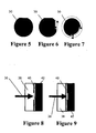
- Figure 5 is a top plan view of a composite sacrificial template/(Al, Ga, In)N article 30.
- Figure 6 is a corresponding view of the composite sacrificial template/(Al, Ga, In)N article during a rastering lasing operation, in which the laser beam is reciprocatingly traversed across the article, to effect interfacial separation of the sacrificial template from the (Al, Ga, In)N material, and yield the product (Al, Ga, In)N wafer article.
- Figure 7 is a corresponding view of the composite sacrificial template/(Al, Ga, In)N article during a perimeter lasing operation, in which the laser beam is translated in circular motion, beginning at the periphery of the article 30, and continuing successively in step-wise smaller-diameter circular arcs, as shown.
- the laser parting process requires that the laser light reach the interface between the (Al,Ga,In)N and template materials. To accomplish this, the laser radiation must transmit through one of the (Al,Ga,In)N and template materials and be absorbed in the other one of such materials. For (Al,Ga,In)N growth, the path of the laser radiation depends on the nature of the sacrificial template.
- the template is a material such as sapphire having a larger bandgap than (Al,Ga,In)N
- the laser light can be transmitted through the sapphire (referred to as the backside layer or material, since this "side” is the “back” or backing layer during the growth process) and the (Al,Ga,In)N material absorbs the laser beam.
- the laser beam can transmit through the (Al,Ga,In)N material and be absorbed in the sacrificial template.
- the absorbed light causes heating which can act to chemically change either material.
- templates with larger bandgap energy than the (Al,Ga,In)N material would be backside illuminated.
- Illustrative material of construction for the sacrificial template include, without limitation, sapphire, larger bandgap (Al,Ga,In)N, spinel, etc.
- one or more interlayers may be employed to absorb light at the (Al,Ga,In)N/template interface.
- Suitable materials for such interlayers include materials that more readily decompose with heating of adjacent layers, to improve or seed (Al,Ga,In)N growth, or a combination thereof.
- the laser light can pass through either surface of the composite sacrificial template/(Al, Ga, In)N article.
- a 10 micron InGaN layer may be grown on the sapphire surface and then a thick GaN layer grown upon the InGaN. Light that is readily absorbed in the InGaN layer for purposes of effecting a chemical or physical change to the InGaN layer will also easily pass through the GaN or sapphire layer.
- the dopants Si, O or Ge may be used to create a heavily n-type doped (Al, Ga, In)N layer that will more readily absorb incident radiation.
- the dopants Mg, Zn, Be may be used to create a heavily p-type doped (Al, Ga, In)N layer that will more readily absorb incident radiation.
- dopant concentrations in excess 1x10 18 cm -3 are preferred.
- a highly defective region such as may be found in GaN on sapphire, can provide a reduction in the bandgap.
- the backside or frontside illuminated templates may be uniform or alternatively they may be patterned to permit laser parting in specific areas. Patterning of the sacrificial template, or use of patterned interlayers, may for instance be employed to facilitate lateral epitaxial overgrowth (LEO), as a technique for defect reduction, or to facilitate slip or cracking in a preferred direction.
- LEO lateral epitaxial overgrowth
- Interlayers can be chosen, for example, so that they can be selectively etched or decomposed, to separate the grown (Al, Ga, In)N from the sacrificial template. Alternately, interlayers can be chosen to couple to a heating source or otherwise to facilitate chemical or physical changes that facilitate parting of the (Al,Ga,In)N material.
- Figure 8 for example is a schematic depiction of a composite sacrificial template/(Al, Ga, In)N article including sacrificial template layer 38 and (Al, Ga, In)N layer 42, separated by interlayer 40, wherein laser beam 36 is impinging on the interlayer to effect decomposition of the interlayer and release the sacrificial template layer 38 from the (Al, Ga, In)N layer 42.
- Figure 9 is a schematic depiction of a composite sacrificial template/(Al, Ga, In)N article including sacrificial template layer 38 and (Al, Ga, In)N layer 42, separated by interlayer 40, wherein laser beam 36 impinging on the interlayer is absorbed by the interlayer.
- the laser beam energy absorbed by the interlayer induces decomposition of the (Al, Ga, In)N material that is adjacent to the interlayer.
- Such decomposition of the (Al, Ga, In)N material releases the sacrificial template layer 38 from the (Al, Ga, In)N layer 42.
- the requirement that the light be transmitted to the (Al,Ga,In)N-template interface means that the laser must be directed to the interface either from the (Al,Ga,In)N side or template side of the composite sacrificial template/(Al, Ga, In)N article, depending on the template material and laser.
- the template material and the laser energy employed for the parting are therefore desirably selected so that the pathway for the laser beam, through the template (for template-side lasing of the composite sacrificial template/(Al, Ga, In)N article) or through the (Al, Ga, In)N material (in the case of (Al, Ga, In)N-side lasing of the composite sacrificial template/(Al, Ga, In)N article) does not significantly hinder (absorb or reflect) the beam.
- a UV laser is employed for template-side lasing of the composite sacrificial template/(Al, Ga, In)N article, then the template is desirably highly transparent to the UV radiation produced by the laser.
- the laser beam pathway through the room ambient (the environment between the generated laser beam and the composite sacrificial template/(Al, Ga, In)N article must also be considered in ensuring that the beam impinged on the article is of suitable character (intensity) to effect parting of the template and (Al, Ga, In)N. Further, the incident angle of the laser beam must not be so shallow that the light is reflected by intervening surfaces.
- a UV laser is employed, and UV transparent quartz is usefully employed directly at the backside of the composite sacrificial template/(Al, Ga, In)N article and transmits the UV laser radiation.
- UV transparent quartz is usefully employed directly at the backside of the composite sacrificial template/(Al, Ga, In)N article and transmits the UV laser radiation.
- sapphire, AlN or other materials transparent to the light used for parting can be used, but these materials must also be compatible with their location in the growth chamber (reactor).
- the composite sacrificial template/(Al, Ga, In)N article may be disposed in an HVPE reactor and may be exposed to corrosive gases and high temperatures and the template material must therefore be compatible (e.g., retain structural integrity for supporting the (Al, Ga, In)N material being grown thereon, as well as transmissivity for the lasing energy being directed to the interface region of the composite article) with the reactor environment.
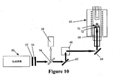
- Figure 10 is a schematic illustration of an in situ laser parting apparatus for conducting growth of (Al,Ga,In)N by HVPE and transmission of laser light to the composite sacrificial template/(Al, Ga, In)N article from the backside of the composite (through the template).
- the laser 50 is arranged with a waveplate 52 and polarizer 54 for power modulation to provide radiation of appropriate character for the parting.
- the laser beam is shown in Figure 10 by the large schematic arrows.
- the beam may be measured as to its power by mirror 56 and associated energy meter 58, which are in place only during power measurement.
- the power measurement may therefore be employed to characterize the laser beam so that appropriate waveplate 52 and polarizer 54 positions/settings are utilized for power modulation.
- the laser beam in normal operation during parting impinges on the mirror 62 and is reflected to the x-y scanner 60.
- the x-y scanner 60 selectively translates the laser beam, directing it to mirror 64 from which it is directed through the pedestal 68 mounted in the (Al, Ga, In)N growth reactor 66.
- the composite wafer article is disposed on the pedestal 68 and comprises (Al, Ga, In)N layer 70 grown on the sacrificial template 72.
- the sacrificial template is transparent to the laser beam, so that the beam passing through the pedestal 68 then is transmitted through the sacrificial template 72 to the template/(Al, Ga, In)N interface.
- the laser energy is absorbed at the interface to effect parting of the sacrificial template 72 from the (Al, Ga, In)N material, to yield (Al, Ga, In)N material in the form of a free-standing (Al, Ga, In)N single crystal article.
- the growth reactor 66 may be constructed and arranged to carry out HVPE as above discussed, or alternatively, a growth reactor constructed and arranged for another (Al, Ga, In)N growth process may be employed, e.g., to carry out MOVPE, CVD, MBE or method or technique known in the art for deposition/growth of (Al, Ga, In)N materials on substrates.
- the pathway of the laser beam is unobstructed for the entire cross-sectional area of the composite sacrificial template/(Al, Ga, In)N article on the pedestal 68.
- This in turn requires a pedestal with a suitably large cross sectional area, so that the beam can be scanned through the entire growth area of the (Al, Ga, In)N layer formed on the template.
- the composite sacrificial template/(Al, Ga, In)N article on the pedestal can be rotated and moved to part the entire growth area of (Al, Ga, In)N material.
- Laser deflection and wafer movements can also be combined (e.g., rotation of the composite sacrificial template/(Al, Ga, In)N article may be effected, with the laser beam deflected to scan from edge to center).
- one or more transparent baffle plates can be placed at the lower end of the pedestal.
- the pedestal 68 since it is utilized as a support structure for the composite sacrificial template/(Al, Ga, In)N article, is preferably highly transparent to the laser beam.
- the pedestal may for example be formed of a UV transparent quartz to enable light to be transmitted to the composite sacrificial template/(Al, Ga, In)N article.
- Such quartz material preferably is bubble-free and contains minimal particulates, in order to be non-absorbent of the incident laser radiation.
- Alternative materials of construction that are transparent, or at least highly transmissive, to UV radiation could alternatively be employed.
- suitable materials of construction for the pedestal can readily be determined within the skill of the art.
- the use of transparent backside materials in the composite sacrificial template/(Al, Ga, In)N article have an additional advantage in that the growth process can be directly monitored during deposition of (Al, Ga, In)N on the sacrificial template, and such monitoring can be employed to control the growth process via feedback control means and techniques.
- Such feedback loop operation is readily implemented, as part of an overall process control sub-system for the (Al, Ga, In)N growth and in situ parting system.
- the surface of the pedestal or other reactor wall material, or even the sacrificial template back surface of the composite sacrificial template/(Al, Ga, In)N article may be modified to shape the light beam being transmitted to the sacrificial template/(Al, Ga, In)N interface of the composite article.
- such surface(s) may be roughened to diffuse the incident beam, or they may be shaped into a series of microlenses to facilitate focusing in specific areas, or they may be masked to prevent illumination in some areas.
- the growth reactor is suitably constructed of materials that are compatible with the growth environment, which may by way of example include growth conditions of temperatures of up to 1200°C, the presence of vapor phase reagents such as NH 3 , HCl, and GaCl, and pressure levels that may variously be subatmospheric, superatmospheric, or atmospheric pressures.
- the template upon which the (Al,Ga,In)N is grown must be transparent to the laser radiation, as previously discussed, and the backside of the template and composite wafer article holder (e.g., the pedestal and any wafer mount or positioning elements used therewith) must be maintained free from laser absorbing deposits such as backside (Al,Ga,In)N.
- the illustrative system schematically depicted in Figure 10 is designed to enable the wafer to stay in the same position for growth and template removal. Such arrangement minimizes temperature change between the growth and template removal operations.
- the growth and template removal process may also be carried out by growing the (Al, Ga, In)N layer on the sacrificial template in one or several chambers or portions of the reactor and transporting the resulting composite wafer article to a separate template removal chamber or area.
- the composite wafer article may be heated during transport to minimize temperature change.
- the template removal operation may be carried out by directing laser light to the frontside of the composite sacrificial template/(Al, Ga, In)N article, in a corresponding manner to the backside illumination approaches discussed hereinabove, using an appropriate laser (and wavelength of lasing energy) to transmit the laser beam through the (Al,Ga,In)N and thermally decompose an interlayer or template, for example.
- the backside of the template and composite wafer article holder are preferably maintained free from laser absorbing deposits, and it is also beneficial to inhibit deposits on the side and the top surface edge of the composite article to facilitate the LILO process when employed in the practice of methods as disclosed herein. If the same gases that deposit (Al,Ga,In)N material make their way to the back of the sacrificial template and react, the resulting deposits can prevent the laser beam from reaching the parting interface. To avoid such adverse consequence and minimize the occurrence of backside deposits, the following approaches may be employed.
- the composite wafer article may be fixedly held from the backside, by vacuum, electrostatic force or other means or techniques that do not block or severely attenuate the laser radiation and that hold the composite wafer article tightly enough against the flat composite wafer article holder to block growth gas flow from reaching the backside of the sacrificial template.
- the backside of the sacrificial template in the composite wafer article can be flushed with inert gas, to direct growth gas flow away from the back of the sacrificial template or to inhibit reaction at the back surface.
- materials such as borosilicate glasses, which are transparent to the laser radiation, which soften or melt at growth and template removal temperatures, and which do not outgas significant impurities or react with the growth process gases, can be used to seal the backside from growth process gases (e.g., source reagent gases, product gases of the growth process, and any associated carrier, diluent, etc., gases).
- growth process gases e.g., source reagent gases, product gases of the growth process, and any associated carrier, diluent, etc., gases.
- Suitable glasses may be provided in the shape of the composite wafer article, or the glasses can be coated on the backside of the sacrificial template before growth. Glass materials can also be used to alter stress and a glass of specific TCE can be correspondingly chosen to minimize stress or induce a desired stress in the composite wafer article. Glass materials may be used to cover the entire backside of the sacrificial template, or they can be utilized to cover the perimeter of the sacrificial template and thereby act
- the backside of the sacrificial template and composite wafer article holder can be coated with a material which inhibits deposits, such as for example sputtered, evaporated, or plasma-enhanced chemical vapor deposition (PECVD)-applied SiO 2 or Si 3 N 4 .
- a material which inhibits deposits such as for example sputtered, evaporated, or plasma-enhanced chemical vapor deposition (PECVD)-applied SiO 2 or Si 3 N 4 .
- PECVD plasma-enhanced chemical vapor deposition
- the inhibiting layer could be removed (e.g., by in situ etching or other technique for removal of the growth inhibiting layer) before parting, thereby removing any deposits that may be present, at the same time.
- cover plates may be utilized, having opening(s) that enable growth to occur at the frontside of the composite wafer article, but preventing significant growth from occurring on the backside of the composite wafer article.
- the cover plate is advantageously formed and deployed so that it enables laser light to reach the interface of the growth region while at the same time enabling release of gases that are produced in the parting operation.
- grooves may be provided in the cover plate to provide a path for gas release.
- the cover plate may be advantageously tapered to provide a shadow effect and serve to reduce deposition of (Al,Ga,In)N on the cover plate during growth.
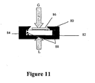
- Figure 11 is a schematic representation of a portion of a growth and parting system using a cover plate 80 on a wafer holder 82.
- the sacrificial template 84 is disposed on the wafer holder 82, and the (Al, Ga, In)N material 86 is grown on the sacrificial template by delivery of the source gases in the gas flow stream indicated schematically in Figure 11 by arrow G.
- the cover plate 80 is tapered as shown, so that deposits 88 of absorbing material produced in the growth process are localized in a manner that does not interfere with the transmission of laser energy to the interface between the sacrificial template 84 and the (Al, Ga, In)N material being grown on the template.
- the laser beam schematically represented in Figure 11 by arrow L, is non-interferingly transmitted through the template to the interface.
- the cover plate thereby shadows the template from adverse growth effects, and the taper of the surface from the top opening of the cover plate (downwardly divergent passage profile) minimizes adherence of the (Al, Ga, In)N material to the cover plate.
- the top surface of the template may be shaped in such a way to facilitate gas escape during the parting process while also inhibiting growth on the template surface.
- One means of accomplishing this is by deposition of an SiO 2 layer on the edge of the template surface and then patterning the SiO 2 layer to expose the template material, thereby forming trenches. If the aspect ratio (ratio of height of the trench to the width of the trench) is sufficiently high, little or no (Al, Ga, In)N will form in the trench.
- the trenches may for example be arranged to form an array of radial grooves to facilitate gas escape from the interface region. Alternatively, the patterning to form the trenches may be carried out so that the grooves are branched, to facilitate gas release during parting.
- cracked nitrogen e.g., atomic N, or NH 3
- HCl can be added to the localized environment of the parting process to assist in removal of Group III elements left behind by the decomposition reactions at the interface.
- decomposition may occur at the backside of the composite wafer article and prevent light from reaching the interface.
- continuous laser operation and etching with HCl may be employed to clear a pathway to the interface.
- the parting environment may suitably be carried out in an environment such as N 2 atmosphere.
- the metal will reflect the laser light from the already parted region, preventing further damage to the interfacial region by the intense light exposure. By monitoring light reflected from the reflective surface, the lift-off progress may be monitored.
- the pressure in the apparatus in which the parting is carried out can be controlled to balance the stress during parting.
- subatmospheric conditions in the chamber in which parting is conducted may help to effectuate gas release from the parting interface.
- pressures in a range of from about 1.3 x 10 -4 Pa to about 1 x 10 6 MPa (about 10 -6 Torr to about 10 10 Torr) are compatible with and preferred in the parting process.
- Higher pressures may require higher decomposition temperatures (more aggressive heating or laser energies).
- localized pressure in the parting operation may be > 133 kPa (> 1000 Torr), particularly if the growth process was conducted at high pressure.
- the thicknesses of the (Al,Ga,In)N material and template layer can be adjusted to minimize stress in the composite wafer article comprising the template and (Al, Ga, In)N materials. Stress is typically present in the (Al,Ga,In)N - template system at the growth temperature because of different material properties of the film and template. In general, thin sacrificial templates will develop stress defects and crack more readily than thicker layers, since relative stress accumulated in thinner layers will cause cracking, which functions to release the stress. Thicker sacrificial templates will bow less and are more readily reuseable.
- the self-supporting nature of the product (Al,Ga,In)N material is dependent on the area of the free-standing material. Larger area (Al, Ga, In)N articles require relatively larger thicknesses to be self-supporting.
- the material quality of the product (Al,Ga,In)N in general, improves with increasing thickness when grown on a foreign template ("foreign" in such context meaning heterogeneous to the (Al, Ga, In)N product material).
- thinner films can be partially parted and therefore partially supported by the sacrificial template. If the unparted area is ⁇ 50% of the total area, thermal stresses induced by cooldown to ambient temperature (e.g., room temperature) can complete the parting process.
- ambient temperature e.g., room temperature
- a weakened interface facilitating parting may also be created by inducing local heating of the composite template/(Al, Ga, In)N article at a temperature that is slightly less (e.g., ⁇ 5 °C below) the thermal decomposition temperature (threshold temperature).
- the parting can be assisted after growth by chemical or physical removal of the sacrificial template. It is also within the purview of methods disclosed herein to combine various approaches for parting the (Al, Ga, In)N and sacrificial template materials from one another, such as for example, by laser parting in combination with chemical etching, or by other combinations of thermal/physical/chemical steps.
- the timing of the parting process relative to the growth process can be varied to maximize material quality, manage the stresses produced in the material, and improve process manufacturability of the (Al, Ga, In)N free-standing single crystal product article.
- the parting process can be performed upon completion of the (Al,Ga,In)N growth, e.g., after 100 to 1000 ⁇ m of (Al,Ga,In)N have been grown on the sacrificial substrate.
- the parting can occur after growth is complete or during the growth process.
- the flexibility of performing the parting during the growth process enables process variations to be effected, such as partially parting the materials at very thin (Al,Ga,In)N thickness and then continuing growth.
- Partial parting can facilitate stress release while enough material is retained to support the (Al,Ga,In)N material during growth. Since thermal decomposition incident to laser irradiation releases gaseous decomposition products at the interface, partial parting by use of lower laser power density, will reduce gas production and reduce cracking.
- the partially parted (Al,Ga,In)N may be completely removed upon completion of growth by further laser parting, by fracture of the unparted material during cooldown, or by other suitable thermal, mechanical and/or chemical means.
- full parting can be carried out with (Al,Ga,In)N thicknesses greater than 20 ⁇ m over a small area.
- Subsequent heating may be also employed to complete the parting or to part the materials again in the event that further growth reattaches the (Al,Ga,In)N to the template or reactor components.
- the parting process may be repeated one or multiple times during the growth process and/or thereafter.
- HCl or other suitable reagent may be employed to remove excess Group III elelments (Al, In, Ga) present after decomposition that may block further laser transmission to the interface of the template/(Al, Ga, In)N article.
- growth can be temporarily interrupted to carry out the parting operation. This sequence can also be repeated one or more times during a full sequence of growth-parting alternating steps.
- the parting process is advantageously carried out upon completion of from about 0.01 to about 100 mm of growth, depending on the desired (Al, Ga, In)N product.
- the parting process is most preferably and beneficially carried out at a temperature at or near the growth temperature, before cooling the reactor containing the template/(Al, Ga, In)N article to ambient temperature (e.g., room temperature)
- the parting processes can also be carried out after the template/(Al,Ga,In)N article has been cooled to ambient temperature.
- the parting operation can be conducted at any suitable temperature, as will be readily determinable within the skill of the art based on the disclosure herein.
- Parting can be performed at elevated temperatures that are greater than, less than, equal to, or substantially equal to, the original temperature at which the (Al,Ga,In)N was grown on the sacrificial template. Parting is suitably carried out at temperatures that are, in order of increasing preference, within 400°C, within 300°C, within 250°C, within 200°C, within 150°C, within 100°C, within 75°C, and within 50°C, of the growth temperature of the (Al, Ga, In)N material on the template.
- An elevated temperature condition of the template/(Al, Ga, In)N composite article is advantageous to at least partially alleviate the TCE-stresses, so that parting at the elevated temperature condition produces a stress-free or substantially stress-free (Al, Ga, In)N free-standing article. Protection of the AlGaInN from thermal decomposition may be necessary, as for example may be effected with the use of an N-containing ambient environment.
- backside deposits are preferably minimized with sputtered or PECVD SiO 2 or other growth inhibitors during the growth of (Al, Ga, In)N on the template.
- the inhibitor in such instances can be chemically removed before parting. Removal of the growth inhibitor layer has the added benefit of removing any backside deposits with it.
- SiO 2 thicknesses greater than 50 nm are preferred, and thicknesses greater than 300 nm are most preferred.
- Prevention of backside deposits and deposits at the edges of the composite template/(Al, Ga, In)N article is advantageously carried out by methods described above for in situ parting (e.g., where parting is carried out in the reactor used to carry out the growth process). Ex situ parting may also be performed, wherein the composite template/(Al, Ga, In)N article is removed from the reactor to carry out subsequent parting. Ex situ parting removes the requirement, inherent in in situ parting, of not blocking the laser beam. Further, the use of ex situ parting entails additional flexibility in use and deployment of means to protect edge and backside portions of the composite template/(Al, Ga, In)N article.
- Physically or chemically removing the edges of the composite template/(Al, Ga, In)N article after growth, to eliminate thick (Al,Ga,In)N growth at the edges of the composite article, may also be used as a processing technique to prevent such adhered areas from causing cracking of the product (Al, Ga, In)N article.
- Physical techniques for such excess growth removal may for example include, without limitation, grinding, cutting, or cleaving along crystalline planes. Chemical removal of such excess growth may be accomplished by etching (in H 3 PO 4 or in HCl) or with UV light-assisted etching of the deposits, where UV light focused on particular areas increases the rate and extent of the etching.
- Laser parameters for impingement of laser energy on the interface of the composite template/(Al, Ga, In)N article in ex situ parting are similar to those used for in situ parting.
- Scanning patterns including initiation of scanning at the edges of composite template/(Al, Ga, In)N articles, are particularly important for release of effused gases in ex situ parting. Since more strain is present in the composite template/(Al, Ga, In)N article in ex situ parting, scanning along crystal planes is more important than for scanning to effect in situ parting. Single beam parting is advantageously employed in instances where lasers are available with sufficient beam size and beam power density to part the entire area, without scanning being necessary.
- (Al,Ga,In)N layers that are too thin to be self-supporting, can be supported by gravity or by bonding to a suitable physical support structure before parting.
- Ex situ parting has the advantage of ready access to the frontside and backside of the composite template/(Al, Ga, In)N article.
- the directional accessibility increases the degrees of freedom for choice of templates and interlayers for ex situ parting operations.
- interlayers that reduce strain and cracking are highly advantageous.
- the interlayer may be provided on the sacrificial template prior to introduction of the template to the growth reactor, or alternatively, the interlayer may be applied in situ in the growth chamber prior to the inception of active growth of the (Al, Ga, In)N material.
- Subthreshold/partial parting of thin layers may be employed in the broad practice of methods disclosed herein, to provide residual surface artifacts as seeds for subsequent growth.
- Subthreshold/partial parting of thick layers followed by chemical etching of the weakened interface also may be utilized as a technique to improve process yield.
- Gases released from the interface during the parting can cause film cracking, reducing process yield.
- Using lower power density reduces the amount of gas released, and reduces the probability of wafer cracking during the parting process.
- the (Al, Ga, In)N article may need to be cleaned to remove residual Group III metals resulting from the interfacial decomposition.
- Acids such as HCl or HF, employed at room temperature or elevated temperature, are effective for this purpose.
- a slow cooling process at a rate ⁇ 10 °C/min. is desirable, although more rapid cooling can be used to improve manufacturability.
- the cooling rate appropriate to obtain a given end product (Al, Ga, In)N article of desired character may readily be determined without undue experimentation, by empirical variation of time-temperature schedules, and morphological characterization and end use testing of the (Al,Ga,In)N product article.
- heating or excitation of the entire sample uniformly (not just locally at the interface), but including an intermediate layer which weakens at a lesser level of heating or excitation is intended to be comprehended by methods disclosed herein.
- the methods disclosed herein are not thus limited, and the (Al, Ga, In)N product article may also include, or have associated therewith, further epitaxial layers, device structures, device precursors, other deposited materials, or devices made from such materials, so long as they do not preclude interfacial processing to effect delamination of template and (Al, Ga, In)N portions of the composite template/(Al, Ga, In)N article.
- These aforementioned layers, structures, precursors, and materials may be deposited before or after the parting has been performed, as necessary and/or appropriate to the end use of the (Al, Ga, In)N article. Systems containing these structures are also contemplated in the broad practice of methods disclosed herein.
- methods disclosed herein have been primarily described herein with reference to (Al,Ga,In)N materials on sacrificial templates, methods disclosed herein are intended to broadly encompass heterogeneous composite material structures having an interface between discrete phases or types of materials, in which the interface is susceptible of energetic or other modification to part the material at the interface region into discrete constituent parts, including composite material structures that may be processed at elevated temperature for interface modification to interfacially delaminate the composite body into constituent parts, or corresponding composite material structures that are interfacially delaminated at ambient temperature after elevated temperature processing and cooldown.
- Free-standing GaN of 400 ⁇ m thickness was produced by HVPE growth of GaN on sapphire, and laser parting of the composite GaN/sapphire article in the growth chamber near the HVPE growth temperature.
- a sacrificial (0001) sapphire wafer was loaded into the growth chamber of an HVPE reactor.
- the sapphire was heated to approximately 1000°C, and the surface of the sapphire was exposed to GaCl gas and NH 3 gas for 165 minutes.
- the GaCl was formed by HCl flowing over molten Ga.
- the NH 3 /HCl ratio was 23.
- the GaCl flow was terminated, and the GaN-sapphire composite was controlled near the growth temperature and at atmospheric pressure, with NH 3 flow maintained to protect the GaN surface.
- Parting radiation for interfacial delamination of the GaN and sapphire layers was generated by a Nd:YAG laser.
- the 3 rd harmonic of the Nd:YAG laser was adjusted to 90 mJ, using a laser power meter and waveplate-polarizer combination.
- the laser radiation was directed to the GaN-sapphire interface through a UV-transmissive quartz pedestal and the sapphire template.
- the GaN-sapphire composite was rotated and the laser beam was electro-optically modulated to scan the beam from edge to center until the entire wafer area was exposed.
- the GaN and sapphire were cooled to room ambient.
- Freestanding GaN and sacrificial sapphire were removed from the growth chamber.
- the resulting freestanding GaN material was approximately 400 ⁇ m in thickness, visibly transparent and crack-free, had a dislocation density less than 10 7 cm -2 and a (0004) double crystal x-ray rocking curve halfwidth of less than 200 arcsec.
- a 40 mm diameter freestanding GaN wafer was produced by HVPE growth of GaN on sapphire, and laser parting at elevated temperature.
- the finished 40 mm diameter, freestanding GaN wafer was approximately 200 ⁇ m in thickness, visibly transparent and crack-free, had a dislocation density of approximately 2 x 10 7 cm -2 , and a root mean square surface roughness of less than 1 nm.
Claims (13)
- Procédé de formation d'un article de (Al, Ga, In)N auto-porteur par étapes comprenant :l'amorçage de la croissance de matière de (Al, Ga, In)N sur un modèle sacrificiel compatible de façon épitaxiale ;la séparation partielle de ladite matière initialement cultivée de (Al, Ga, In)N sur ledit modèle sacrificiel compatible de façon épitaxiale ;la croissance ininterrompue de ladite matière de (Al, Ga, In)N sur ledit modèle sacrificiel compatible de façon épitaxiale ;l'achèvement suivant de ladite croissance de matière de (Al, Ga, In)N, l'achèvement de l'enlèvement de ladite matière de (Al, Ga, In)N depuis ledit modèle sacrificiel compatible de façon épitaxiale pour donner une matière de (Al, Ga, In)N auto-porteuse.
- Procédé selon la revendication 1, dans lequel au moins un de ladite séparation partielle et dudit enlèvement de matière de (AI, Ga, In)N depuis ledit modèle sacrificiel compatible de façon épitaxiale est effectué en transmettant un faisceau laser à une interface entre ladite matière de (Al, Ga, In)N et ledit modèle sacrificiel compatible de façon épitaxiale.
- Procédé selon la revendication 2, dans lequel ladite croissance de matière de (Al, Ga, In)N sur ledit modèle sacrificiel compatible de façon épitaxiale est effectuée dans un réacteur de croissance comprenant une matière transparente à un faisceau laser, et ladite transmission du faisceau laser comprend la transmission du faisceau laser à travers la matière transparente du réacteur de croissance jusqu'à une interface entre ladite matière de (Al, Ga, In)N et ledit modèle sacrificiel compatible de façon épitaxiale.
- Procédé selon la revendication 1, dans lequel ladite croissance de matière de (Al, Ga, In)N sur ledit modèle sacrificiel compatible de façon épitaxiale est effectuée dans un réacteur de croissance, et dans lequel ledit enlèvement de ladite matière de (Al, Ga, In)N depuis ledit modèle sacrificiel compatible de façon épitaxiale est effectué dans ledit réacteur de croissance.
- Procédé selon l'une quelconque des revendications 3 ou 4, dans lequel le réacteur de croissance comprend un piédestal conçu pour supporter le modèle sacrificiel compatible de façon épitaxiale, et le procédé comprend en outre la rotation du piédestal pendant au moins une des étapes de séparation partielle et d'enlèvement.
- Procédé selon la revendication 1, dans lequel l'enlèvement de ladite matière de (Al, Ga, In)N depuis ledit modèle sacrificiel compatible de façon épitaxiale est achevé par au moins un de ce qui suit : refroidissement jusqu'à température ambiante, gravure chimique, et séparation par laser.
- Procédé selon la revendication 1, dans lequel :ladite séparation partielle inclut n'importe laquelle due : (a) séparation par laser, (b) gravure chimique, (c) frappe d'énergie acoustique sur une interface entre ladite matière de (Al, Ga, In)N et ledit modèle sacrificiel compatible de façon épitaxiale, (d) frappe sur ladite interface d'un milieu de frappe sélectionné à partir du groupe constitué de protons, d'ions et de faisceaux de particules, et (e) couplage RF avec ladite interface ; etl'achèvement de l'enlèvement de ladite matière de (Al, Ga, In)N depuis le modèle sacrificiel compatible de façon épitaxiale inclut n'importe lequel de : (i) séparation par laser, (ii) gravure chimique, (iii) frappe d'énergie acoustique sur ladite interface, (iv) frappe sur ladite interface d'un milieu de frappe sélectionné à partir du groupe constitué de protons, d'ions et de faisceaux de particules, (v) couplage RF avec ladite interface, et (vi) refroidissement de la matière de (Al, Ga, In)N à température ambiante.
- Procédé selon l'une quelconque des revendications 1 à 7, dans lequel ladite croissance de matière de (Al, Ga, In)N comprend au moins une d'une épitaxie en phase vapeur d'hydrures (HVPE), une épitaxie en phase vapeur organométallique (MOVPE), un dépôt chimique en phase vapeur (CVD), et une épitaxie par faisceau moléculaire (MBE).
- Procédé selon la revendication 1, dans lequel ladite séparation partielle est effectuée à une température qui est dans les limites de 300 °C de la température à laquelle ladite matière de (Al, Ga, In)N est cultivée sur ledit modèle sacrificiel compatible de façon épitaxiale.
- Procédé selon la revendication 1, comprenant en outre la formation d'une intercouche entre le modèle sacrificiel compatible de façon épitaxiale et ladite matière de (Al, Ga, In)N.
- Procédé selon la revendication 1, dans lequel après ladite séparation partielle, une matière suffisante de (Al, Ga, In)N reste au niveau d'une interface entre ladite matière de (Al, Ga, In)N et ledit modèle sacrificiel compatible de façon épitaxiale pour supporter ladite matière de (Al, Ga, In)N.
- Procédé selon la revendication 1, dans lequel la matière de (Al, Ga, In)N comprend une matière de (Al, Ga, In)N monocristalline.
- Procédé selon la revendication 1, comprenant en outre la formation de l'article de (Al, Ga, In)N auto-porteur dans des plaquettes ayant une épaisseur d'environ 100 à environ 1 000 µm.
Priority Applications (1)
| Application Number | Priority Date | Filing Date | Title |
|---|---|---|---|
| EP10011142.6A EP2287368B1 (fr) | 2001-09-05 | 2002-08-12 | Appareil et procédé pour produire du (Al, Ga, In)N en utilisant un laser in-situ pour la séparation de ce materiau |
Applications Claiming Priority (2)
| Application Number | Priority Date | Filing Date | Title |
|---|---|---|---|
| US09/947,253 US6958093B2 (en) | 1994-01-27 | 2001-09-05 | Free-standing (Al, Ga, In)N and parting method for forming same |
| EP02757061A EP1423259B1 (fr) | 2001-09-05 | 2002-08-12 | Procédé de séparation d'un produit (al, ga, in)n autonome |
Related Parent Applications (2)
| Application Number | Title | Priority Date | Filing Date |
|---|---|---|---|
| EP02757061A Division EP1423259B1 (fr) | 2001-09-05 | 2002-08-12 | Procédé de séparation d'un produit (al, ga, in)n autonome |
| EP02757061.3 Division | 2002-08-12 |
Related Child Applications (4)
| Application Number | Title | Priority Date | Filing Date |
|---|---|---|---|
| EP10011142.6A Division EP2287368B1 (fr) | 2001-09-05 | 2002-08-12 | Appareil et procédé pour produire du (Al, Ga, In)N en utilisant un laser in-situ pour la séparation de ce materiau |
| EP10011142.6A Previously-Filed-Application EP2287368B1 (fr) | 2001-09-05 | 2002-08-12 | Appareil et procédé pour produire du (Al, Ga, In)N en utilisant un laser in-situ pour la séparation de ce materiau |
| EP10011142.6A Division-Into EP2287368B1 (fr) | 2001-09-05 | 2002-08-12 | Appareil et procédé pour produire du (Al, Ga, In)N en utilisant un laser in-situ pour la séparation de ce materiau |
| EP10011142.6 Division-Into | 2010-09-28 |
Publications (3)
| Publication Number | Publication Date |
|---|---|
| EP2248931A2 EP2248931A2 (fr) | 2010-11-10 |
| EP2248931A3 EP2248931A3 (fr) | 2011-10-12 |
| EP2248931B1 true EP2248931B1 (fr) | 2015-02-25 |
Family
ID=25485829
Family Applications (3)
| Application Number | Title | Priority Date | Filing Date |
|---|---|---|---|
| EP02757061A Expired - Lifetime EP1423259B1 (fr) | 2001-09-05 | 2002-08-12 | Procédé de séparation d'un produit (al, ga, in)n autonome |
| EP10007964.9A Expired - Lifetime EP2248931B1 (fr) | 2001-09-05 | 2002-08-12 | PROCÉDÉ POUR FORMER UN ARTICLE DE (Al, Ga, In)N AUTOSUPPORTÉ |
| EP10011142.6A Expired - Lifetime EP2287368B1 (fr) | 2001-09-05 | 2002-08-12 | Appareil et procédé pour produire du (Al, Ga, In)N en utilisant un laser in-situ pour la séparation de ce materiau |
Family Applications Before (1)
| Application Number | Title | Priority Date | Filing Date |
|---|---|---|---|
| EP02757061A Expired - Lifetime EP1423259B1 (fr) | 2001-09-05 | 2002-08-12 | Procédé de séparation d'un produit (al, ga, in)n autonome |
Family Applications After (1)
| Application Number | Title | Priority Date | Filing Date |
|---|---|---|---|
| EP10011142.6A Expired - Lifetime EP2287368B1 (fr) | 2001-09-05 | 2002-08-12 | Appareil et procédé pour produire du (Al, Ga, In)N en utilisant un laser in-situ pour la séparation de ce materiau |
Country Status (8)
| Country | Link |
|---|---|
| US (1) | US6958093B2 (fr) |
| EP (3) | EP1423259B1 (fr) |
| JP (3) | JP4401168B2 (fr) |
| KR (2) | KR100979456B1 (fr) |
| CN (3) | CN100420569C (fr) |
| MY (1) | MY130719A (fr) |
| TW (1) | TW593797B (fr) |
| WO (1) | WO2003020497A1 (fr) |
Families Citing this family (80)
| Publication number | Priority date | Publication date | Assignee | Title |
|---|---|---|---|---|
| US6958093B2 (en) * | 1994-01-27 | 2005-10-25 | Cree, Inc. | Free-standing (Al, Ga, In)N and parting method for forming same |
| US5679152A (en) * | 1994-01-27 | 1997-10-21 | Advanced Technology Materials, Inc. | Method of making a single crystals Ga*N article |
| US6596079B1 (en) * | 2000-03-13 | 2003-07-22 | Advanced Technology Materials, Inc. | III-V nitride substrate boule and method of making and using the same |
| TWI226139B (en) * | 2002-01-31 | 2005-01-01 | Osram Opto Semiconductors Gmbh | Method to manufacture a semiconductor-component |
| US8809867B2 (en) * | 2002-04-15 | 2014-08-19 | The Regents Of The University Of California | Dislocation reduction in non-polar III-nitride thin films |
| AU2003223563A1 (en) * | 2002-04-15 | 2003-11-03 | The Regents Of The University Of California | NON-POLAR (A1,B,In,Ga) QUANTUM WELL AND HETEROSTRUCTURE MATERIALS AND DEVICES |
| KR20030090996A (ko) * | 2002-05-24 | 2003-12-01 | 엘지전자 주식회사 | 성장 챔버내에서의 레이저 리프트 오프 방법 |
| JP4363029B2 (ja) * | 2002-11-06 | 2009-11-11 | ソニー株式会社 | 分割波長板フィルターの製造方法 |
| KR100504180B1 (ko) * | 2003-01-29 | 2005-07-28 | 엘지전자 주식회사 | 질화물 화합물 반도체의 결정성장 방법 |
| JP4662918B2 (ja) * | 2003-01-31 | 2011-03-30 | オスラム オプト セミコンダクターズ ゲゼルシャフト ミット ベシュレンクテル ハフツング | 半導体構成素子の製造のための方法 |
| US20060180804A1 (en) * | 2003-01-31 | 2006-08-17 | Peter Stauss | Thin-film semiconductor component and production method for said component |
| JP3534115B1 (ja) * | 2003-04-02 | 2004-06-07 | 住友電気工業株式会社 | エッジ研磨した窒化物半導体基板とエッジ研磨したGaN自立基板及び窒化物半導体基板のエッジ加工方法 |
| US7261777B2 (en) * | 2003-06-06 | 2007-08-28 | S.O.I.Tec Silicon On Insulator Technologies | Method for fabricating an epitaxial substrate |
| EP1484794A1 (fr) * | 2003-06-06 | 2004-12-08 | S.O.I. Tec Silicon on Insulator Technologies S.A. | Procédé de fabrication d'un substrat auto-porté |
| US7170095B2 (en) * | 2003-07-11 | 2007-01-30 | Cree Inc. | Semi-insulating GaN and method of making the same |
| WO2005008740A2 (fr) * | 2003-07-14 | 2005-01-27 | Allegis Technologies, Inc. | Procedes de traitement du nitrure de gallium |
| KR100506739B1 (ko) * | 2003-12-23 | 2005-08-08 | 삼성전기주식회사 | 알루미늄(Al)을 함유한 질화물 반도체 결정 성장방법 |
| JP5194334B2 (ja) * | 2004-05-18 | 2013-05-08 | 住友電気工業株式会社 | Iii族窒化物半導体デバイスの製造方法 |
| WO2006005062A2 (fr) * | 2004-06-30 | 2006-01-12 | Cree, Inc. | Procedes d'encapsulation en boitier-puce de dispositifs electroluminescents et dispositifs electroluminescents encapsules en boitier-puce |
| TWI422044B (zh) * | 2005-06-30 | 2014-01-01 | Cree Inc | 封裝發光裝置之晶片尺度方法及經晶片尺度封裝之發光裝置 |
| US7273798B2 (en) * | 2005-08-01 | 2007-09-25 | Avago Technologies Ecbu Ip (Singapore) Pte. Ltd. | Gallium nitride device substrate containing a lattice parameter altering element |
| DE102005052358A1 (de) * | 2005-09-01 | 2007-03-15 | Osram Opto Semiconductors Gmbh | Verfahren zum lateralen Zertrennen eines Halbleiterwafers und optoelektronisches Bauelement |
| DE102005052357A1 (de) * | 2005-09-01 | 2007-03-15 | Osram Opto Semiconductors Gmbh | Verfahren zum lateralen Zertrennen eines Halbleiterwafers und optoelektronisches Bauelement |
| US7713232B2 (en) | 2005-11-04 | 2010-05-11 | Medrad, Inc. | System for washing and processing of cells for delivery thereof to tissue |
| US8435879B2 (en) | 2005-12-12 | 2013-05-07 | Kyma Technologies, Inc. | Method for making group III nitride articles |
| US8441179B2 (en) | 2006-01-20 | 2013-05-14 | Cree, Inc. | Lighting devices having remote lumiphors that are excited by lumiphor-converted semiconductor excitation sources |
| JP2009524247A (ja) * | 2006-01-20 | 2009-06-25 | クリー エル イー ディー ライティング ソリューションズ インコーポレイテッド | ルミファー膜を空間的に分離することにより固体光発光素子におけるスペクトル内容をシフトすること |
| KR100718118B1 (ko) * | 2006-06-01 | 2007-05-14 | 삼성코닝 주식회사 | 크랙이 없는 GaN 벌크 단결정의 성장 방법 및 장치 |
| WO2007148615A1 (fr) | 2006-06-20 | 2007-12-27 | Sumitomo Electric Industries, Ltd. | Procédé de croissance d'un cristal de AlxGa1-xN, et substrat en cristal de AlxGa1-xN |
| JP5045232B2 (ja) * | 2006-06-20 | 2012-10-10 | 住友電気工業株式会社 | AlxGa1−xN結晶の成長方法 |
| US8698184B2 (en) | 2011-01-21 | 2014-04-15 | Cree, Inc. | Light emitting diodes with low junction temperature and solid state backlight components including light emitting diodes with low junction temperature |
| WO2008024385A2 (fr) | 2006-08-23 | 2008-02-28 | Cree Led Lighting Solutions, Inc. | Dispositif d'éclairage et procédé d'éclairage |
| US9416464B1 (en) | 2006-10-11 | 2016-08-16 | Ostendo Technologies, Inc. | Apparatus and methods for controlling gas flows in a HVPE reactor |
| US8557042B2 (en) * | 2006-12-08 | 2013-10-15 | Saint-Gobain Cristaux Et Detecteurs | Method for manufacturing a single crystal of nitride by epitaxial growth on a substrate preventing growth on the edges of the substrate |
| JP4899911B2 (ja) * | 2007-02-16 | 2012-03-21 | 日立電線株式会社 | Iii族窒化物半導体基板 |
| US20080303033A1 (en) | 2007-06-05 | 2008-12-11 | Cree, Inc. | Formation of nitride-based optoelectronic and electronic device structures on lattice-matched substrates |
| US7863635B2 (en) * | 2007-08-07 | 2011-01-04 | Cree, Inc. | Semiconductor light emitting devices with applied wavelength conversion materials |
| US20120125256A1 (en) * | 2007-10-06 | 2012-05-24 | Solexel, Inc. | Apparatus and method for repeatedly fabricating thin film semiconductor substrates using a template |
| US20090108269A1 (en) * | 2007-10-26 | 2009-04-30 | Led Lighting Fixtures, Inc. | Illumination device having one or more lumiphors, and methods of fabricating same |
| JP5262203B2 (ja) | 2008-03-11 | 2013-08-14 | 住友電気工業株式会社 | 化合物半導体単結晶の製造装置および製造方法 |
| DE102008001005B4 (de) | 2008-04-04 | 2011-06-22 | Karlsruher Institut für Technologie, 76131 | Verfahren zur Herstellung eines Schichtverbundes mit epitaktisch gewachsenen Schichten aus einem magnetischen Formgedächtnis-Material und Schichtverbund mit epitaktischen Schichten aus einem magnetischen Formgedächtnis-Material sowie dessen Verwendung |
| KR20110063773A (ko) * | 2008-09-24 | 2011-06-14 | 에스.오.아이. 테크 실리콘 온 인슐레이터 테크놀로지스 | 릴랙싱된 반도체 재료층들을 형성하는 방법들, 반도체 구조들, 디바이스들 및 그를 포함하는 엔지니어링된 기판들 |
| CN102203904B (zh) | 2008-10-30 | 2013-11-20 | S.O.I.探测硅绝缘技术公司 | 形成具有减小的晶格应变的半导体材料层、半导体结构、装置的方法及包含具有减小的晶格应变的半导体材料层、半导体结构、装置的工程衬底 |
| US8637383B2 (en) | 2010-12-23 | 2014-01-28 | Soitec | Strain relaxation using metal materials and related structures |
| CN101740331B (zh) * | 2008-11-07 | 2012-01-25 | 东莞市中镓半导体科技有限公司 | 利用固体激光器无损剥离GaN与蓝宝石衬底的方法 |
| CN101555627B (zh) * | 2009-04-30 | 2012-01-25 | 苏州纳晶光电有限公司 | 一种氮化镓基外延膜的激光剥离方法 |
| CN101879657B (zh) * | 2009-05-08 | 2016-06-29 | 东莞市中镓半导体科技有限公司 | 固体激光剥离设备和剥离方法 |
| US8921876B2 (en) | 2009-06-02 | 2014-12-30 | Cree, Inc. | Lighting devices with discrete lumiphor-bearing regions within or on a surface of remote elements |
| JP5349260B2 (ja) * | 2009-11-19 | 2013-11-20 | 株式会社東芝 | 半導体発光装置及びその製造方法 |
| TWI412487B (zh) * | 2009-12-31 | 2013-10-21 | Huang Chung Cheng | 奈米線結構的製造方法 |
| US9275979B2 (en) | 2010-03-03 | 2016-03-01 | Cree, Inc. | Enhanced color rendering index emitter through phosphor separation |
| TWI442455B (zh) | 2010-03-29 | 2014-06-21 | Soitec Silicon On Insulator | Iii-v族半導體結構及其形成方法 |
| FR2961719B1 (fr) * | 2010-06-24 | 2013-09-27 | Soitec Silicon On Insulator | Procede de traitement d'une piece en un materiau compose |
| WO2012046478A1 (fr) * | 2010-10-06 | 2012-04-12 | ウシオ電機株式会社 | Procédé d'arrachement au laser et dispositif d'arrachement au laser |
| JP2011151400A (ja) * | 2011-02-10 | 2011-08-04 | Furukawa Co Ltd | レーザ剥離装置、レーザ剥離方法、iii族窒化物半導体自立基板の製造方法 |
| JP2011159980A (ja) * | 2011-02-10 | 2011-08-18 | Furukawa Co Ltd | レーザ剥離装置、レーザ剥離方法、iii族窒化物半導体自立基板の製造方法 |
| US11251164B2 (en) | 2011-02-16 | 2022-02-15 | Creeled, Inc. | Multi-layer conversion material for down conversion in solid state lighting |
| US8841207B2 (en) * | 2011-04-08 | 2014-09-23 | Lux Material Co., Ltd. | Reusable substrates for electronic device fabrication and methods thereof |
| RU2013156438A (ru) * | 2011-05-31 | 2015-07-10 | ООО "Совершенные кристаллы" | Способ и устройство для изготовления обособленных кристаллов нитридов элементов iii группы |
| RU2593868C2 (ru) * | 2011-05-31 | 2016-08-10 | ООО "Совершенные кристаллы" | Способ и устройство для изготовления обособленных кристаллов нитридов элементов iii группы |
| US9136794B2 (en) | 2011-06-22 | 2015-09-15 | Research Triangle Institute, International | Bipolar microelectronic device |
| JP6117199B2 (ja) * | 2011-06-28 | 2017-04-19 | サン‐ゴバン、クリストー、エ、デテクトゥールSaint−Gobain Cristaux & Detecteurs | 半導体基板及び形成する方法 |
| CN104040675A (zh) * | 2011-09-29 | 2014-09-10 | 氮化物处理股份有限公司 | 无机材料、制作其的方法和装置、及其使用 |
| KR20130081956A (ko) * | 2012-01-10 | 2013-07-18 | 삼성전자주식회사 | 질화물 반도체층 성장 방법 |
| WO2013139887A1 (fr) * | 2012-03-21 | 2013-09-26 | Freiberger Compound Materials Gmbh | Procédé de production de monocristaux de iii-n, et monocristaux de iii-n |
| JP6024533B2 (ja) | 2012-03-28 | 2016-11-16 | 日亜化学工業株式会社 | サファイア基板及びその製造方法並びに窒化物半導体発光素子 |
| JP6144525B2 (ja) * | 2013-04-05 | 2017-06-07 | 古河機械金属株式会社 | 下地基板の製造方法およびiii族窒化物半導体基板の製造方法 |
| US9831363B2 (en) * | 2014-06-19 | 2017-11-28 | John Farah | Laser epitaxial lift-off of high efficiency solar cell |
| FR3009644B1 (fr) | 2013-08-08 | 2016-12-23 | Soitec Silicon On Insulator | Procede, empilement et ensemble de separation d'une structure d'un substrat par irradiations electromagnetiques |
| CN107305947B (zh) * | 2016-04-25 | 2022-01-04 | 松下知识产权经营株式会社 | 电池和电池系统 |
| CN109307613B (zh) * | 2018-10-18 | 2021-07-02 | 中国石油天然气股份有限公司 | 一种制备人造岩心的方法及装置 |
| KR102001791B1 (ko) * | 2018-12-26 | 2019-07-18 | 한양대학교 산학협력단 | 이온 주입을 이용한 질화갈륨 기판 제조 방법 |
| US10576585B1 (en) | 2018-12-29 | 2020-03-03 | Cree, Inc. | Laser-assisted method for parting crystalline material |
| US10562130B1 (en) | 2018-12-29 | 2020-02-18 | Cree, Inc. | Laser-assisted method for parting crystalline material |
| US11024501B2 (en) | 2018-12-29 | 2021-06-01 | Cree, Inc. | Carrier-assisted method for parting crystalline material along laser damage region |
| US10611052B1 (en) | 2019-05-17 | 2020-04-07 | Cree, Inc. | Silicon carbide wafers with relaxed positive bow and related methods |
| JP2023510554A (ja) * | 2020-01-16 | 2023-03-14 | エスエルティー テクノロジーズ インコーポレイテッド | 高品質iii族金属窒化物種結晶およびその製造方法 |
| KR20220006880A (ko) * | 2020-07-09 | 2022-01-18 | 주식회사루미지엔테크 | 단결정 기판의 제조 방법 |
| CN112975117B (zh) * | 2020-08-27 | 2022-09-13 | 重庆康佳光电技术研究院有限公司 | 一种激光剥离方法及装置 |
| CN112382735B (zh) * | 2020-11-17 | 2021-11-12 | 东莞赣锋电子有限公司 | 一种激光清洗制备锂离子电池极片的方法 |
Family Cites Families (43)
| Publication number | Priority date | Publication date | Assignee | Title |
|---|---|---|---|---|
| US3326820A (en) | 1965-04-22 | 1967-06-20 | Ibm | Arc process for forming high melting point compounds |
| NL6615059A (fr) | 1966-10-25 | 1968-04-26 | ||
| US3598526A (en) | 1967-04-27 | 1971-08-10 | Dow Chemical Co | Method for preparing monocrystalline aluminum nitride |
| US3829556A (en) | 1972-03-24 | 1974-08-13 | Bell Telephone Labor Inc | Growth of gallium nitride crystals |
| US3922703A (en) | 1974-04-03 | 1975-11-25 | Rca Corp | Electroluminescent semiconductor device |
| JPS5659700A (en) | 1979-10-17 | 1981-05-23 | Matsushita Electric Ind Co Ltd | Forming method for gallium nitride single crystal thin film |
| EP0193830A3 (fr) | 1980-04-10 | 1986-10-01 | Massachusetts Institute Of Technology | Dispositif à cellules solaires comportant plusieurs cellules solaires constitutives |
| US4622083A (en) | 1985-03-11 | 1986-11-11 | Texas Instruments Incorporated | Molecular beam epitaxial process |
| US5373171A (en) | 1987-03-12 | 1994-12-13 | Sumitomo Electric Industries, Ltd. | Thin film single crystal substrate |
| US4931132A (en) | 1988-10-07 | 1990-06-05 | Bell Communications Research, Inc. | Optical control of deposition of crystal monolayers |
| US5006914A (en) | 1988-12-02 | 1991-04-09 | Advanced Technology Materials, Inc. | Single crystal semiconductor substrate articles and semiconductor devices comprising same |
| US4985742A (en) | 1989-07-07 | 1991-01-15 | University Of Colorado Foundation, Inc. | High temperature semiconductor devices having at least one gallium nitride layer |
| US5433169A (en) | 1990-10-25 | 1995-07-18 | Nichia Chemical Industries, Ltd. | Method of depositing a gallium nitride-based III-V group compound semiconductor crystal layer |
| US5334277A (en) | 1990-10-25 | 1994-08-02 | Nichia Kagaky Kogyo K.K. | Method of vapor-growing semiconductor crystal and apparatus for vapor-growing the same |
| US5146465A (en) | 1991-02-01 | 1992-09-08 | Apa Optics, Inc. | Aluminum gallium nitride laser |
| EP0576566B1 (fr) | 1991-03-18 | 1999-05-26 | Trustees Of Boston University | Procede de preparation et de dopage de couches minces de nitrure de gallium monocristallin tres isolant |
| DE69221806T2 (de) * | 1991-10-10 | 1998-03-26 | Coherent Inc | Vorrichtung zum Abgeben eines defokussierten Laserstrahls mit scharfkantigem Querschnitt |
| JP3352712B2 (ja) | 1991-12-18 | 2002-12-03 | 浩 天野 | 窒化ガリウム系半導体素子及びその製造方法 |
| JPH07267796A (ja) * | 1994-03-31 | 1995-10-17 | Mitsubishi Cable Ind Ltd | GaN単結晶の製造方法 |
| US5846844A (en) | 1993-11-29 | 1998-12-08 | Toyoda Gosei Co., Ltd. | Method for producing group III nitride compound semiconductor substrates using ZnO release layers |
| JPH07202265A (ja) * | 1993-12-27 | 1995-08-04 | Toyoda Gosei Co Ltd | Iii族窒化物半導体の製造方法 |
| US6958093B2 (en) * | 1994-01-27 | 2005-10-25 | Cree, Inc. | Free-standing (Al, Ga, In)N and parting method for forming same |
| US6440823B1 (en) * | 1994-01-27 | 2002-08-27 | Advanced Technology Materials, Inc. | Low defect density (Ga, Al, In)N and HVPE process for making same |
| US5679152A (en) * | 1994-01-27 | 1997-10-21 | Advanced Technology Materials, Inc. | Method of making a single crystals Ga*N article |
| DE19640594B4 (de) | 1996-10-01 | 2016-08-04 | Osram Gmbh | Bauelement |
| US5954874A (en) | 1996-10-17 | 1999-09-21 | Hunter; Charles Eric | Growth of bulk single crystals of aluminum nitride from a melt |
| EP1007768A4 (fr) | 1997-07-03 | 2003-07-16 | Cbl Technologies | Elimination des defauts d'inadequation thermique que presentent des films de depot epitaxique en separant le substrat du film a la temperature de croissance |
| US6071795A (en) | 1998-01-23 | 2000-06-06 | The Regents Of The University Of California | Separation of thin films from transparent substrates by selective optical processing |
| US6331208B1 (en) * | 1998-05-15 | 2001-12-18 | Canon Kabushiki Kaisha | Process for producing solar cell, process for producing thin-film semiconductor, process for separating thin-film semiconductor, and process for forming semiconductor |
| TW417315B (en) * | 1998-06-18 | 2001-01-01 | Sumitomo Electric Industries | GaN single crystal substrate and its manufacture method of the same |
| JP3525061B2 (ja) * | 1998-09-25 | 2004-05-10 | 株式会社東芝 | 半導体発光素子の製造方法 |
| US6280523B1 (en) * | 1999-02-05 | 2001-08-28 | Lumileds Lighting, U.S., Llc | Thickness tailoring of wafer bonded AlxGayInzN structures by laser melting |
| JP2000228539A (ja) * | 1999-02-08 | 2000-08-15 | Sharp Corp | 窒素化合物半導体の製造方法 |
| US6176925B1 (en) * | 1999-05-07 | 2001-01-23 | Cbl Technologies, Inc. | Detached and inverted epitaxial regrowth & methods |
| KR20010029199A (ko) * | 1999-09-30 | 2001-04-06 | 홍세경 | 질화물 단결정 기판 제조 장치 및 방법 |
| JP3518455B2 (ja) * | 1999-12-15 | 2004-04-12 | 日亜化学工業株式会社 | 窒化物半導体基板の作製方法 |
| US6380108B1 (en) * | 1999-12-21 | 2002-04-30 | North Carolina State University | Pendeoepitaxial methods of fabricating gallium nitride semiconductor layers on weak posts, and gallium nitride semiconductor structures fabricated thereby |
| JP3568112B2 (ja) * | 1999-12-27 | 2004-09-22 | 豊田合成株式会社 | 半導体基板の製造方法 |
| KR20010058673A (ko) * | 1999-12-30 | 2001-07-06 | 이형도 | 하이드라이드 기상 에피택시 성장법에 의한 크랙없는갈륨나이트라이드 후막 제조 방법 |
| US6447604B1 (en) * | 2000-03-13 | 2002-09-10 | Advanced Technology Materials, Inc. | Method for achieving improved epitaxy quality (surface texture and defect density) on free-standing (aluminum, indium, gallium) nitride ((al,in,ga)n) substrates for opto-electronic and electronic devices |
| US6596079B1 (en) * | 2000-03-13 | 2003-07-22 | Advanced Technology Materials, Inc. | III-V nitride substrate boule and method of making and using the same |
| US6652648B2 (en) * | 2000-04-27 | 2003-11-25 | Samsung Corning Co., Ltd. | Method for fabricating GaN single crystal substrate |
| JP3803606B2 (ja) * | 2001-04-13 | 2006-08-02 | 松下電器産業株式会社 | Iii族窒化物半導体基板の製造方法 |
-
2001
- 2001-09-05 US US09/947,253 patent/US6958093B2/en not_active Expired - Fee Related
-
2002
- 2002-08-12 KR KR1020097013810A patent/KR100979456B1/ko active IP Right Grant
- 2002-08-12 EP EP02757061A patent/EP1423259B1/fr not_active Expired - Lifetime
- 2002-08-12 CN CNB028174798A patent/CN100420569C/zh not_active Expired - Lifetime
- 2002-08-12 JP JP2003524788A patent/JP4401168B2/ja not_active Expired - Lifetime
- 2002-08-12 EP EP10007964.9A patent/EP2248931B1/fr not_active Expired - Lifetime
- 2002-08-12 CN CN2008101301585A patent/CN101353813B/zh not_active Expired - Lifetime
- 2002-08-12 WO PCT/US2002/025412 patent/WO2003020497A1/fr active Application Filing
- 2002-08-12 KR KR1020047003318A patent/KR100921409B1/ko active IP Right Grant
- 2002-08-12 EP EP10011142.6A patent/EP2287368B1/fr not_active Expired - Lifetime
- 2002-08-12 CN CN201110301148.5A patent/CN102383193B/zh not_active Expired - Lifetime
- 2002-08-27 MY MYPI20023185A patent/MY130719A/en unknown
- 2002-09-03 TW TW091120025A patent/TW593797B/zh not_active IP Right Cessation
-
2008
- 2008-04-11 JP JP2008103245A patent/JP4958833B2/ja not_active Expired - Lifetime
-
2011
- 2011-10-19 JP JP2011229598A patent/JP5580803B2/ja not_active Expired - Lifetime
Also Published As
| Publication number | Publication date |
|---|---|
| EP1423259A1 (fr) | 2004-06-02 |
| JP4958833B2 (ja) | 2012-06-20 |
| KR20040045431A (ko) | 2004-06-01 |
| EP2287368B1 (fr) | 2018-04-18 |
| EP1423259B1 (fr) | 2010-08-04 |
| KR20090082515A (ko) | 2009-07-30 |
| EP2248931A3 (fr) | 2011-10-12 |
| EP2287368A2 (fr) | 2011-02-23 |
| CN100420569C (zh) | 2008-09-24 |
| MY130719A (en) | 2007-07-31 |
| JP4401168B2 (ja) | 2010-01-20 |
| CN101353813A (zh) | 2009-01-28 |
| KR100921409B1 (ko) | 2009-10-14 |
| CN102383193A (zh) | 2012-03-21 |
| JP5580803B2 (ja) | 2014-08-27 |
| EP2287368A3 (fr) | 2013-10-09 |
| EP1423259A4 (fr) | 2007-06-27 |
| WO2003020497A1 (fr) | 2003-03-13 |
| EP2248931A2 (fr) | 2010-11-10 |
| JP2005502193A (ja) | 2005-01-20 |
| CN1551824A (zh) | 2004-12-01 |
| CN102383193B (zh) | 2014-11-26 |
| US20020068201A1 (en) | 2002-06-06 |
| TW593797B (en) | 2004-06-21 |
| KR100979456B1 (ko) | 2010-09-02 |
| US6958093B2 (en) | 2005-10-25 |
| JP2012051792A (ja) | 2012-03-15 |
| CN101353813B (zh) | 2012-06-27 |
| JP2008273825A (ja) | 2008-11-13 |
Similar Documents
| Publication | Publication Date | Title |
|---|---|---|
| EP2248931B1 (fr) | PROCÉDÉ POUR FORMER UN ARTICLE DE (Al, Ga, In)N AUTOSUPPORTÉ | |
| US6617261B2 (en) | Structure and method for fabricating GaN substrates from trench patterned GaN layers on sapphire substrates | |
| JP3721674B2 (ja) | 窒化物系iii−v族化合物半導体基板の製造方法 | |
| US6559075B1 (en) | Method of separating two layers of material from one another and electronic components produced using this process | |
| US6498113B1 (en) | Free standing substrates by laser-induced decoherency and regrowth | |
| US6596377B1 (en) | Thin film product and method of forming | |
| KR100616656B1 (ko) | 질화갈륨계 단결정 기판의 제조방법 및 제조장치 | |
| US20060234486A1 (en) | Wafer separation technique for the fabrication of free-standing (Al,In,Ga)N wafers | |
| JP2016029008A (ja) | 高品質ホモエピタキシ用微傾斜窒化ガリウム基板 | |
| US6902989B2 (en) | Method for manufacturing gallium nitride (GaN) based single crystalline substrate that include separating from a growth substrate |
Legal Events
| Date | Code | Title | Description |
|---|---|---|---|
| PUAI | Public reference made under article 153(3) epc to a published international application that has entered the european phase |
Free format text: ORIGINAL CODE: 0009012 |
|
| AC | Divisional application: reference to earlier application |
Ref document number: 1423259 Country of ref document: EP Kind code of ref document: P |
|
| AK | Designated contracting states |
Kind code of ref document: A2 Designated state(s): FR GB |
|
| RIN1 | Information on inventor provided before grant (corrected) |
Inventor name: BRANDES, GEORGE R. Inventor name: KELLY, MICHAEL K. Inventor name: TISCHLER, MICHAEL A. Inventor name: VAUDO, ROBERT P. |
|
| RIN1 | Information on inventor provided before grant (corrected) |
Inventor name: BRANDES, GEORGE R. Inventor name: TISCHLER, MICHAEL A. Inventor name: KELLY, MICHAEL K. Inventor name: VAUDO, ROBERT P. |
|
| PUAL | Search report despatched |
Free format text: ORIGINAL CODE: 0009013 |
|
| AK | Designated contracting states |
Kind code of ref document: A3 Designated state(s): FR GB |
|
| RIC1 | Information provided on ipc code assigned before grant |
Ipc: C30B 25/02 20060101ALI20110906BHEP Ipc: C30B 29/38 20060101ALI20110906BHEP Ipc: C30B 29/10 20060101ALI20110906BHEP Ipc: C30B 23/00 20060101AFI20110906BHEP Ipc: C30B 25/18 20060101ALI20110906BHEP Ipc: C30B 29/40 20060101ALI20110906BHEP Ipc: C30B 28/14 20060101ALI20110906BHEP Ipc: C30B 25/00 20060101ALI20110906BHEP Ipc: C30B 28/12 20060101ALI20110906BHEP |
|
| 17P | Request for examination filed |
Effective date: 20120412 |
|
| 17Q | First examination report despatched |
Effective date: 20120904 |
|
| RIC1 | Information provided on ipc code assigned before grant |
Ipc: C30B 25/00 20060101ALI20140807BHEP Ipc: C30B 25/02 20060101ALI20140807BHEP Ipc: C30B 33/00 20060101ALI20140807BHEP Ipc: C30B 25/18 20060101ALI20140807BHEP Ipc: H01L 21/02 20060101ALI20140807BHEP Ipc: C30B 23/00 20060101AFI20140807BHEP Ipc: C30B 29/40 20060101ALI20140807BHEP Ipc: H01L 33/00 20100101ALI20140807BHEP |
|
| GRAP | Despatch of communication of intention to grant a patent |
Free format text: ORIGINAL CODE: EPIDOSNIGR1 |
|
| INTG | Intention to grant announced |
Effective date: 20140915 |
|
| RIN1 | Information on inventor provided before grant (corrected) |
Inventor name: TISCHLER, MICHAEL A. Inventor name: KELLY, MICHAEL K. Inventor name: VAUDO, ROBERT P. Inventor name: BRANDES, GEORGE R. |
|
| GRAS | Grant fee paid |
Free format text: ORIGINAL CODE: EPIDOSNIGR3 |
|
| GRAA | (expected) grant |
Free format text: ORIGINAL CODE: 0009210 |
|
| AC | Divisional application: reference to earlier application |
Ref document number: 1423259 Country of ref document: EP Kind code of ref document: P |
|
| AK | Designated contracting states |
Kind code of ref document: B1 Designated state(s): FR GB |
|
| REG | Reference to a national code |
Ref country code: GB Ref legal event code: FG4D |
|
| PLBE | No opposition filed within time limit |
Free format text: ORIGINAL CODE: 0009261 |
|
| STAA | Information on the status of an ep patent application or granted ep patent |
Free format text: STATUS: NO OPPOSITION FILED WITHIN TIME LIMIT |
|
| 26N | No opposition filed |
Effective date: 20151126 |
|
| GBPC | Gb: european patent ceased through non-payment of renewal fee |
Effective date: 20150812 |
|
| REG | Reference to a national code |
Ref country code: FR Ref legal event code: PLFP Year of fee payment: 15 |
|
| PG25 | Lapsed in a contracting state [announced via postgrant information from national office to epo] |
Ref country code: GB Free format text: LAPSE BECAUSE OF NON-PAYMENT OF DUE FEES Effective date: 20150812 |
|
| REG | Reference to a national code |
Ref country code: FR Ref legal event code: PLFP Year of fee payment: 16 |
|
| REG | Reference to a national code |
Ref country code: FR Ref legal event code: PLFP Year of fee payment: 17 |
|
| PGFP | Annual fee paid to national office [announced via postgrant information from national office to epo] |
Ref country code: FR Payment date: 20210825 Year of fee payment: 20 |