EP2203946B1 - Frit sealing with a variable laser beam - Google Patents
Frit sealing with a variable laser beam Download PDFInfo
- Publication number
- EP2203946B1 EP2203946B1 EP08836683.6A EP08836683A EP2203946B1 EP 2203946 B1 EP2203946 B1 EP 2203946B1 EP 08836683 A EP08836683 A EP 08836683A EP 2203946 B1 EP2203946 B1 EP 2203946B1
- Authority
- EP
- European Patent Office
- Prior art keywords
- sealing
- laser beam
- oled
- frit
- laser
- Prior art date
- Legal status (The legal status is an assumption and is not a legal conclusion. Google has not performed a legal analysis and makes no representation as to the accuracy of the status listed.)
- Not-in-force
Links
Images


Classifications
-
- B—PERFORMING OPERATIONS; TRANSPORTING
- B23—MACHINE TOOLS; METAL-WORKING NOT OTHERWISE PROVIDED FOR
- B23K—SOLDERING OR UNSOLDERING; WELDING; CLADDING OR PLATING BY SOLDERING OR WELDING; CUTTING BY APPLYING HEAT LOCALLY, e.g. FLAME CUTTING; WORKING BY LASER BEAM
- B23K26/00—Working by laser beam, e.g. welding, cutting or boring
- B23K26/08—Devices involving relative movement between laser beam and workpiece
-
- B—PERFORMING OPERATIONS; TRANSPORTING
- B23—MACHINE TOOLS; METAL-WORKING NOT OTHERWISE PROVIDED FOR
- B23K—SOLDERING OR UNSOLDERING; WELDING; CLADDING OR PLATING BY SOLDERING OR WELDING; CUTTING BY APPLYING HEAT LOCALLY, e.g. FLAME CUTTING; WORKING BY LASER BEAM
- B23K26/00—Working by laser beam, e.g. welding, cutting or boring
- B23K26/20—Bonding
- B23K26/206—Laser sealing
-
- B—PERFORMING OPERATIONS; TRANSPORTING
- B23—MACHINE TOOLS; METAL-WORKING NOT OTHERWISE PROVIDED FOR
- B23K—SOLDERING OR UNSOLDERING; WELDING; CLADDING OR PLATING BY SOLDERING OR WELDING; CUTTING BY APPLYING HEAT LOCALLY, e.g. FLAME CUTTING; WORKING BY LASER BEAM
- B23K26/00—Working by laser beam, e.g. welding, cutting or boring
- B23K26/20—Bonding
- B23K26/32—Bonding taking account of the properties of the material involved
- B23K26/324—Bonding taking account of the properties of the material involved involving non-metallic parts
-
- H—ELECTRICITY
- H05—ELECTRIC TECHNIQUES NOT OTHERWISE PROVIDED FOR
- H05B—ELECTRIC HEATING; ELECTRIC LIGHT SOURCES NOT OTHERWISE PROVIDED FOR; CIRCUIT ARRANGEMENTS FOR ELECTRIC LIGHT SOURCES, IN GENERAL
- H05B33/00—Electroluminescent light sources
- H05B33/02—Details
- H05B33/04—Sealing arrangements, e.g. against humidity
-
- H—ELECTRICITY
- H10—SEMICONDUCTOR DEVICES; ELECTRIC SOLID-STATE DEVICES NOT OTHERWISE PROVIDED FOR
- H10K—ORGANIC ELECTRIC SOLID-STATE DEVICES
- H10K50/00—Organic light-emitting devices
- H10K50/80—Constructional details
- H10K50/84—Passivation; Containers; Encapsulations
-
- H—ELECTRICITY
- H10—SEMICONDUCTOR DEVICES; ELECTRIC SOLID-STATE DEVICES NOT OTHERWISE PROVIDED FOR
- H10K—ORGANIC ELECTRIC SOLID-STATE DEVICES
- H10K50/00—Organic light-emitting devices
- H10K50/80—Constructional details
- H10K50/84—Passivation; Containers; Encapsulations
- H10K50/842—Containers
- H10K50/8426—Peripheral sealing arrangements, e.g. adhesives, sealants
-
- B—PERFORMING OPERATIONS; TRANSPORTING
- B23—MACHINE TOOLS; METAL-WORKING NOT OTHERWISE PROVIDED FOR
- B23K—SOLDERING OR UNSOLDERING; WELDING; CLADDING OR PLATING BY SOLDERING OR WELDING; CUTTING BY APPLYING HEAT LOCALLY, e.g. FLAME CUTTING; WORKING BY LASER BEAM
- B23K2101/00—Articles made by soldering, welding or cutting
- B23K2101/36—Electric or electronic devices
-
- B—PERFORMING OPERATIONS; TRANSPORTING
- B23—MACHINE TOOLS; METAL-WORKING NOT OTHERWISE PROVIDED FOR
- B23K—SOLDERING OR UNSOLDERING; WELDING; CLADDING OR PLATING BY SOLDERING OR WELDING; CUTTING BY APPLYING HEAT LOCALLY, e.g. FLAME CUTTING; WORKING BY LASER BEAM
- B23K2103/00—Materials to be soldered, welded or cut
- B23K2103/50—Inorganic materials other than metals or composite materials
- B23K2103/54—Glass
Definitions
- the present invention is directed to sealing Organic Light Emitting Diodes (OLEDs) and displays made of OLEDs.
- OLEDs Organic Light Emitting Diodes
- OLEDs organic light-emitting diodes
- OLEDs include electrodes and organic layers. There are two types of electrodes an anode and a cathode. There are also two types of organic layers a conducting layer and an emissive layer.
- the OLED components are deployed on a first substrate.
- the first substrate is typically made of clear plastic, glass, or foil.
- a second substrate that is made of similar material is used to cover the OLED.
- the first substrate and the second substrate are hermitically sealed with a frit, encasing the OLED in a package (i.e., glass package).
- the anode and the cathode i.e., two electrodes
- the anode and the cathode facilitate the flow of current through the glass package.
- charge carriers holes and electrons
- photons are produced to generate light.
- OLEDs are considered as the replacement technology for the next generation of Liquid Crystal Display (LCD) and Light Emitting Diode (LED) based applications.
- LCD Liquid Crystal Display
- LED Light Emitting Diode
- Conventional OLEDs have a number of advantages. For example, OLEDs are found to be thinner, lighter, and more flexible than the crystalline layers in an LED or LCD. Since the light-emitting layers of an OLED are lighter, the substrate of an OLED can be flexible instead of rigid. In addition, OLEDs are brighter than LEDs, do not require backlighting like LCDs, and consume much less power than LCDs. These advantages are especially important for battery-operated devices such as cell phones and mobile computers. Lastly, OLEDs are easier to produce, can be made to large sizes, and have large fields of view. As a result of these advantages, current applications for OLEDs include small-screen devices such as cell phones, personal data assistants (PDAs), digital cameras, as well as large-screen applications such as the big-screen televisions of
- OLEDs do have a number of shortcomings.
- Conventional OLED manufacturing is very expensive.
- One issue is that OLEDs are susceptible to damage from exposure to the atmosphere. Exposing the organic layers to moisture and oxygen may cause a reduction in the useful life of an OLED. For example, OLED performance rapidly degrades in the presence of even a minute amount of moisture. To address this problem, during manufacturing, an OLED must be hermetically sealed.
- hermetic sealing is accomplished by dispensing a frit pattern between two substrates and melting and sealing the frit to create a hermetically sealed airtight glass package.
- Conventional methods of melting and sealing the frit pattern are performed with a laser.
- the frit pattern must be dispensed on the substrate far enough away from the organic material so that the laser sealing process does not cause a thermal defect in the organic material.
- non-uniform laser characteristics may cause thermal damage. For example, if the laser changes in intensity profile, power, or beam size, etc., the laser may cause a non-uniform bond across the width, and length of the frit pattern, resulting in a poor hermetic seal.
- One conventional method of laser sealing uses an optical mask to mitigate the problems associated with sealing across electrical leads and the thermal effects that result from sealing.
- the mask reduces useful laser power for sealing and as a result, impacts the quality of the seal and time required for sealing.
- quality and time impact the cost to manufacture and the useful life of an OLED-based product.
- WO 2007/067533 A2 discloses a method of sealing comprising a substrate and a frit pattern, wherein a laser beam is focused onto the frit pattern.
- US 2006/082298 A1 discloses a method of sealing an OLED using a diffuser to convert a laser beam, focusing the laser beam onto a frit pattern and changing at least one the characteristic of the laser beam as the laser beam traverses the frit pattern.
- the present invention provides a method of sealing an OLED according to claim 1.
- a beam shaper dynamically adjusts various characteristics of the laser beam and laser operations such as the shape, size and the intensity profile to achieve a stronger and more uniform, hermetic, laser seal of an OLED.
- the beam shaper comprises an optical system that enables dynamic changes to characteristics of the laser beam such as the laser beam shape and intensity profile in real-time during the sealing process. As such the laser beam shape and intensity profile is adjusted during sealing to accommodate electrical leads, changes in the frit pattern, and the thermal issues associated with laser sealing an OLED.
- the beam shaper is implemented with several lenses that can be used in combination to change beam shape and several characteristics of the beam.
- the beam shaper provides variable beam shapes without requiring an optical mask to achieve high speed, uniform hermetic sealing of OLED devices.
- the beam size in both the x and y directions can be independently adjusted to match a frit pattern including corner curvature, directional changes, and height variation of the frit pattern.
- both the laser power and the sealing speed may also be dynamically adjusted and vary along the frit pattern to achieve the best sealing performance.
- the beam shaper may comprise a first lens, a second lens, a distance between the first lens and the second lens, and a diffuser
- the method may comprise the steps of generating a first laser beam spot with the beam shaper; traversing a frit pattern with the first laser beam spot; and generating a second laser beam spot with the beam shaper during traversal of the frit pattern.
- a beam shaper capable of achieving unique beam intensity profiles such as flat-top, annular, M-shaped, with different shapes such as rectangular, circular, and elliptical is provided.
- the beam shaper is implemented by inserting an optical diffuser between the lenses of an optical system to redistribute laser beam intensity.
- the beam intensity profile is controlled by the diffuser while the beam size and shape are controlled by varying the relative distance between the lenses.
- the beam shaper generates an annular beam or M-shaped beam with lower power in the center, higher power at the edges, and a precisely controlled power intensity ratio (i.e., valley to peak ratio).
- a precisely controlled power intensity ratio i.e., valley to peak ratio.
- a beam shaper implemented in accordance with the teachings of the present invention can be used to meet all requirements for hermetic sealing of OLED devices.
- the beam shaper provides improved flexibility, productivity, better sealing performance and mechanical strength.
- the beam shaper produces a variety of beam profiles to match specific frit sizes and patterns.
- the variety of beam profiles eliminates the need for custom masks.
- a sealing system or station implemented in accordance with the teachings of the present invention can be used for mass production of a number of different products.
- the pre-production time is saved and total cost is reduced.
- a beam shaper used in conjunction with low-loss glass materials can be lossless so that most of the laser power can be focused on the frit and sealing speed can be improved.
- a beam shaper implemented in accordance with the teachings of the present invention can result in better sealing performance and stronger mechanical strength.
- the sealing quality can be improved considerably.
- the beam shaper can provide more uniform heating (frit temperature), better utilization of frit width, stronger bonding to the substrate, less thermal effect on the adjacent components, and less damage to the substrate.
- a method for sealing an OLED is presented.
- a method for dynamically shaping a laser beam onto a frit pattern is presented.
- the method enables dynamic shaping of a laser beam and dynamic changes to characteristics of the laser beam in real-time during the laser sealing process. As such, variations in the frit pattern may be accommodated and a better hermetic seal may be achieved.
- a beam shaper is implemented using a plurality of optical lenses (i.e., optical system) that are selected or are adjusted relative to each other to dynamically shape a laser beam in real-time during the sealing process.
- a diffuser is positioned within the optical system and the combination of the optical lenses and the diffuser are selected and/or adjusted to dynamically shape a laser beam footprint (i.e., beam size and shape) and dynamically change the characteristics of the laser beam, such as the shape, size, and the intensity profile in real-time during sealing.
- a laser beam footprint i.e., beam size and shape
- the characteristics of the laser beam such as the shape, size, and the intensity profile in real-time during sealing.
- the optical lenses and the diffuser a variety of beam shapes ranging from elliptical, to square, to donut shaped, etc may be realized.
- the intensity profile may be dynamically changed to address variations in the frit and result in a better seal.
- Fig. 1 displays a schematic diagram of a beam shaper implemented in accordance with the teachings of the present invention.
- a laser beam 1 is applied to seal a frit 8 positioned between a cover substrate 7 and a support substrate 9.
- the laser beam 1 may be generated using a laser system 1A such as a diode laser based system.
- the laser beam 1 may be implemented as single mode beam with diffraction-limited beam quality, or as a multi-mode beam, etc.
- the laser beam 1 is delivered by an optical fiber to an optical system 2.
- the optical fiber can be single mode or multimode fiber. It should be appreciated that a variety of laser beam generating devices may be implemented and are contemplated within the scope of the present invention.
- the optical system 2 includes a number of lenses (3, 5, 6) and a diffuser 4 for shaping the laser beam 1.
- the frit 8 is positioned between a cover substrate 7 and a support substrate 9.
- the optical lenses (3, 5, 6) are adjusted relative to each other to re-image the laser beam 1 to a desirable beam shape and intensity profile.
- a laser beam 1 is re-imaged by the three lenses (3, 5, 6) onto the frit 8 through the cover substrate 7.
- the laser wavelength is chosen for optimal performance of both substrates and frit so that the laser is transparent to the substrates but absorbed by the frit.
- the laser radiation absorbed by the frit 8 leads to rapid local heating to melt the frit 8 and to form a hermetic seal between the two glass substrates (7, 9).
- the laser beam 1 may remain stationary and the substrates (7, 9) and the frit 8 may move.
- the optical system 2 and laser 1 may move and the substrates (7, 9) and frit 8 may remain stationary.
- both the optical system 2 and the substrates (7, 9) may move relative to each other. As a result, the laser continuously melts the frit and finally forms a hermetic seal of the two substrates (7, 9).
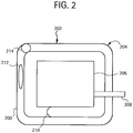
- Fig. 2 displays a variable laser beam traversing along a frit pattern 200.
- Fig 2 displays the frit 8 of Fig. 1 as the frit 8 would look from the top view.
- a frit pattern 200 is shown (i.e., frit 8 of Fig. 1 from a top view).
- the frit pattern 200 changes and includes straight sections shown by 202 and curved sections shown as 204.
- Organic material 206 may be deployed within the boundaries of the frit pattern 200.
- electrical leads 208 may cross the path of the frit pattern 200.
- the organic material 206 is typically spaced from the frit pattern 200 as shown by 210 to avoid thermal effects resulting from the laser sealing.
- the footprint (212, 214) of a variable laser beam is also shown.
- the footprint 212 and the footprint 214 represent the same laser beam (i.e., at different times) reshaped by the beam shaper depicted in Fig. 1 as the laser beam traverses different sections of the frit pattern 200.
- the footprint 212 may represent the variable laser beam as the laser traverses a straight portion 202 of the frit pattern 200. As such, footprint 212 may be implemented as an elliptical beam which may be more appropriate since an elliptical beam may cover more surface area at a higher speed on straight sections 202, while remaining within the boundaries of the straight sections 202.
- the footprint 214 may represent the variable laser beam as the laser traverses the curved portion 214 of the frit pattern 200. As such, footprint 214 may be implemented as a circular beam which may be more appropriate since a circular footprint may provide the appropriate dimensions and maintain uniform beam characteristics as the laser beam traverses the curved sections 204 of the frit pattern 200.
- a laser beam may be implemented with a first footprint such as an elliptical footprint 212, move at a first speed, operate at first power, and include a first intensity profile and, for example, along the curved portion 204 of the frit pattern 200 the laser beam may be implemented with a second footprint such as a circular footprint 214, move at a second speed that is different from the first speed, operate at a power level that is different from the first power level, and provide a second intensity profile that is different from the first intensity profile.
- the laser beam may be dynamically adjusted, in real-time, during sealing, to accommodate any non-uniformity in the frit pattern.
- non-uniformity may include any changes in frit pattern, such as height, width, direction, etc., as well as any additional issues that effect the sealing operations or preclude a strong hermetic seal such as spacing from the organic material, obstructions in the frit pattern, requirements for temperature distribution across the frit (i.e., uniform distribution), proper utilization of frit width, strong bonding strength, thermal effect on the adjacent components, damage to the substrates, etc.
- the OLED is sandwiched between a glass substrate and a cover glass which are sealed together with a frit to form a glass package.
- the frit seal formed by the frit pattern 200 is normally positioned on the outer edge of the glass package.
- the electrical leads 208 pass through the frit pattern 200 and connect to external circuits. The presence of the electrical leads 208 makes the hermetic sealing difficult as the non-transparent electrical leads 208 may cause a variation or discontinuity in the frit pattern 200 and have different absorption properties which may create uneven laser absorption and effect sealing quality.
- the electrical leads 208 also induce different dynamic thermal behavior because of the difference of thermal conductivity.
- the laser power varies when the laser encounters the electrical leads 208 so that the frit temperature can be constant to obtain best sealing quality.
- the beam should be slightly smaller than the frit to avoid unwanted thermal effects on the electrical leads and the organic material 206.
- a laser beam cover a long section of the frit so that it can seal the frit at a higher speed, as there is a relationship between the shape, the power, and the speed of sealing (i.e., traversing the laser beam across the frit pattern). For example, a first beam with a first shape and higher power may traverse the beam faster than a second beam, with a second shape, and lower power.
- changing the shape to elliptical, and adjusting the power, and the speed of sealing reduces residual stress during sealing as the frit can be heated and cooled slower with an elliptical beam than with a small circular beam given that the frit has longer reaction time with the laser beam (i.e., given that the elliptical shape takes a longer time to traverse a spot on the frit) and thus reduces temperature gradient and induced stress.
- Fig. 3 shows an optical system implemented useful for understanding the teachings of the present invention.
- Fig. 3 represents the three lenses (3, 5, 6) of the beam shaper 2 shown in Fig. 1 .
- Lens 302 corresponds to lens 3 of Fig. 1
- lens 304 corresponds to lens 5 of Fig. 1
- lens 306 corresponds to lens 6 of Fig. 1 .
- a light source such as a laser diode 300 generates a laser which traverses through a first lens 302, a second lens 304, to a third lens 306.
- the laser source 300 can be a diode laser or other type of laser, such as Nd:YAG laser, fiber laser, or diode-pumped solid-state laser.
- the laser beam may be transported by an optical fiber.
- the distances of lenses from the laser diode are 15.77mm, 40mm, and 35.6mm, respectively and lens parameters as shown in Table I provided below.
- the optical system of Fig. 3 includes of a number of optical lenses (302, 304, 306) that can provide a variable elliptical beam with aspect ratios ranging from 1.5 to at least 3.0.
- the aspect ratio of the laser beam may be adjusted by varying the distance between the two cylindrical lenses.
- the aspect ratio of the beam is appropriately chosen so that the sealing along the frit is optimal while thermal effect on the adjacent components is minimal.
- a laser diode fiber 300 with a diameter of 1.5 mm can be converted into a 0.8X1.5 mm elliptical beam.
- the elliptical beam can be changed from 0.8X1.5 mm to 0.82X2.2 mm by changing the distance shown as 308 between the lens 302 and 304.
- Table I Lens parameters Lens Type Focal length 302 Cylindrical Plano Convex 25mm 304 Cylindrical Plano Convex 150mm 306 Aspherical Lenses 34.5mm
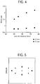
- Fig. 4 displays a plot of the beam size vs. lens location.
- Fig. 4 depicts how a change in the distance between lens 304 and lens 302 of Fig. 3 (i.e., 308 of Fig. 3 ) affects the shape of the laser beam.
- a change in distance between lens 304 and lens 302 substantially changes the beam shape in the Y-axis but has very little impact in the X-axis.
- This unique feature allows the elliptical footprint of the laser beam to change at a corner of a frit pattern as shown in Fig. 2 (i.e., 214) so that it can match the changes and orientation of the frit width enabling the laser beam to traverse the corner with the appropriate laser characteristics and a better hermetic seal.
- the power difference can be estimated using beam size difference when the same laser power is used.
- the frit should move approximately 50% faster at the corner or alternatively the laser power should be approximately 50% lower if a constant speed is desired.
- Fig. 5 displays an example of the beam shape after the beam is reshaped by the beam shaper (i.e., Fig. 1 ).
- the eight dots surrounding a central dot outline the edge of the elliptical beam.
- a circular laser source i.e., 300 of Fig. 3
- two cylindrical lenses (302, 304) are adjusted relative to each other the elliptical beam shown in Fig. 5 may be generated from a curricular laser source (i.e., 300).
- Fig. 6 displays one embodiment of a lens housing for achieving adjustable beam size and shape.
- the lens housing represents the physical apparatus used to implement the beam shaper of Fig. 1 .
- the adjustment of the lenses is achieved by mounting the lenses in the mechanical housing of Fig. 6 .
- the first lens 610 is mounted with respect to a first fiber mount 600 and pre-aligned, while the second cylindrical lens 620 and the aspherical lens 630 are mounted in a different housing.
- distance changes between lenses is achieved by moving the lens 620 and 630 together while keeping the fiber and the lens 610 location unchanged. The distance change can be made manually or by a computer controlled stage.
- each lens housing must have a high precision reference surfaces for registration of the lens position.
- the position tolerance for each lens is normally less than 10 microns.
- each lens can be replaced by a more sophisticated multiple element lens consisting of a number of convex and concave lenses to optimize performance.
- the aspherical lens can also be replaced with a number of spherical lenses to achieve similar functionality.
- the beam size (i.e., footprint) on the frit can be adjusted by defocusing the beam when a large beam is required.
- the beam can be increased to several millimeters.
- a larger beam size can also be achieved by changing the lens focal lengths so that a greater magnification is achieved.
- each cylindrical lens can be replaced with a combination of convex and concave cylindrical lenses so that the effective focal length can be adjusted by varying the distance between the lenses.
- Fig. 7 displays a diffuser implemented in accordance with the teachings of the present invention.
- a diffuser is defined as a diffractive optic element that receive a laser beam and redistribute the light into virtually any pattern desired.
- a diffuser with a microstructure having different shapes and thickness on the surface redirects the input beam by changing the phase of each segment of the beam.
- the diffusers are not sensitive to alignment and do not effect the polarization of the input beam. They can be made out of fused silica, silicon, plastic, or other materials covering wavelengths from 193nm to 20um.
- diffusers implemented in accordance with the teachings of the present invention can be made with minimal zero order hot spots (often less than 1%) and efficiencies as high as 95%.
- the structures that make a diffuser work are called scatter centers. These are the elementary surface units that direct incoming light rays into different directions.
- the clustering of millions of scatter centers over a large area combines to provide the scattering properties of the diffuser.
- the typical scatter center is a microlens element, as illustrated in Fig. 7 .
- each scatter center is individually designed to implement a certain light-control task.
- the surface structure as well the statistical distribution of scatter centers is carefully designed and fabricated.
- a diffuser may be used to adjust a characteristic of the laser beam, such as beam intensity profile, divergence angle, and beam shape.
- the diffuser may be used to adjust the intensity profile of the beam.
- a beam with a unique intensity profile is required such as flat-top and donut-like to optimize seal strength and quality. This can be achieved by inserting a beam diffuser between the lenses.
- a beam having a central deepened intensity profile i.e. M-shaped profile
- the key to achieving such an intensity profile is to choose the diffuser capable of converting a Gaussian intensity profile into an M-shaped profile with minimal residual zero-order (i.e. central peak).
- the diffuser is used to convert a Gaussian beam with higher intensity in the center into a donut-shaped beam with lower intensity in the center than the edges of the beam.
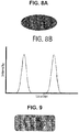
- Fig. 8A displays a beam intensity profile, which is achieved by adding a beam diffuser between the lenses of the beam shaper shown in Fig. 1 .
- Fig. 8B is an example of the intensity profile vs. location.
- the diffuser redistributes power from an original circular beam to the edge and the lenses re-image the beam into an elliptical ring shown as Fig. 8A .
- the beam intensity profile is controlled by the diffuser while the beam size is controlled by the lenses.
- the beam shaper implemented in accordance with the teachings of the present invention (i.e., Fig. 1 ) can control the beam size and power intensity independently.
- the diffuser is used to convert a circular Gaussian beam into a rectangular-like beam with fairly uniform intensity over the beam or slightly higher intensity around the edges as shown in Fig. 9 .
- the aspect ratio is controlled by lens distance as well.
- the beam changes from aspect ratio of approximately 2 ⁇ 4 along the straight portion while it reduces to ⁇ 1 at corners to avoid potential damage to electrical leads and display elements.
- a new beam profile can be constructed.
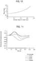
- the power intensity is lower in the center of the laser beam and increases as you move from the center of the laser beam to the edge of the laser beam.
- the ratio of power intensity between frit edge and frit center is 3.23, as shown in Fig. 10 .
- the temperature difference across the frit width is noticeably less than that of conventional approach using a Gaussian beam with an optical mask. This more uniform temperature across the frit width leads to uniform heating of the frit, therefore the bonding of the frit to the substrate is more uniform across the width, and better utilization of frit width is achieved.
- the laser power is reduced when the beam passes through the area including electrical leads across the frit while the sealing speed remains unchanged.
- the frit volume in the region is smaller than that of region without electrical leads, reducing power can avoid overheating of the region and thus prevent the electrical leads from potential damage.
- the power reduction is dependent on the size and material of both frit and electrical leads. Normally, the power should be reduced to less than 15%, preferably, less than 10%.
Landscapes
- Physics & Mathematics (AREA)
- Optics & Photonics (AREA)
- Engineering & Computer Science (AREA)
- Plasma & Fusion (AREA)
- Mechanical Engineering (AREA)
- Electroluminescent Light Sources (AREA)
Applications Claiming Priority (2)
| Application Number | Priority Date | Filing Date | Title |
|---|---|---|---|
| US11/904,696 US8247730B2 (en) | 2007-09-28 | 2007-09-28 | Method and apparatus for frit sealing with a variable laser beam |
| PCT/US2008/011140 WO2009045320A2 (en) | 2007-09-28 | 2008-09-25 | Frit sealing with a variable laser beam |
Publications (2)
| Publication Number | Publication Date |
|---|---|
| EP2203946A2 EP2203946A2 (en) | 2010-07-07 |
| EP2203946B1 true EP2203946B1 (en) | 2018-07-11 |
Family
ID=40091977
Family Applications (1)
| Application Number | Title | Priority Date | Filing Date |
|---|---|---|---|
| EP08836683.6A Not-in-force EP2203946B1 (en) | 2007-09-28 | 2008-09-25 | Frit sealing with a variable laser beam |
Country Status (7)
| Country | Link |
|---|---|
| US (1) | US8247730B2 (enExample) |
| EP (1) | EP2203946B1 (enExample) |
| JP (1) | JP5323843B2 (enExample) |
| KR (1) | KR101359060B1 (enExample) |
| CN (1) | CN101842918B (enExample) |
| TW (1) | TWI377863B (enExample) |
| WO (1) | WO2009045320A2 (enExample) |
Families Citing this family (55)
| Publication number | Priority date | Publication date | Assignee | Title |
|---|---|---|---|---|
| JP5308718B2 (ja) | 2008-05-26 | 2013-10-09 | 浜松ホトニクス株式会社 | ガラス溶着方法 |
| DE112009001347T5 (de) * | 2008-06-11 | 2011-04-21 | Hamamatsu Photonics K.K., Hamamatsu | Schmelzverbindungsprozess für Glas |
| KR101651300B1 (ko) * | 2008-06-23 | 2016-08-25 | 하마마츠 포토닉스 가부시키가이샤 | 유리 용착 방법 |
| US8198564B2 (en) | 2008-09-09 | 2012-06-12 | Electro Scientific Industries, Inc. | Adaptive optic beamshaping in laser processing systems |
| US8440479B2 (en) * | 2009-05-28 | 2013-05-14 | Corning Incorporated | Method for forming an organic light emitting diode device |
| US8568184B2 (en) * | 2009-07-15 | 2013-10-29 | Apple Inc. | Display modules |
| JP5481167B2 (ja) | 2009-11-12 | 2014-04-23 | 浜松ホトニクス株式会社 | ガラス溶着方法 |
| JP5525246B2 (ja) | 2009-11-25 | 2014-06-18 | 浜松ホトニクス株式会社 | ガラス溶着方法及びガラス層定着方法 |
| JP5535590B2 (ja) * | 2009-11-25 | 2014-07-02 | 浜松ホトニクス株式会社 | ガラス溶着方法及びガラス層定着方法 |
| JP5481172B2 (ja) | 2009-11-25 | 2014-04-23 | 浜松ホトニクス株式会社 | ガラス溶着方法及びガラス層定着方法 |
| JP5481173B2 (ja) | 2009-11-25 | 2014-04-23 | 浜松ホトニクス株式会社 | ガラス溶着方法及びガラス層定着方法 |
| JP5567319B2 (ja) * | 2009-11-25 | 2014-08-06 | 浜松ホトニクス株式会社 | ガラス溶着方法及びガラス層定着方法 |
| JP5535588B2 (ja) | 2009-11-25 | 2014-07-02 | 浜松ホトニクス株式会社 | ガラス溶着方法及びガラス層定着方法 |
| JP5466929B2 (ja) | 2009-11-25 | 2014-04-09 | 浜松ホトニクス株式会社 | ガラス溶着方法及びガラス層定着方法 |
| JP5535589B2 (ja) | 2009-11-25 | 2014-07-02 | 浜松ホトニクス株式会社 | ガラス溶着方法及びガラス層定着方法 |
| WO2011067700A1 (en) * | 2009-12-02 | 2011-06-09 | Koninklijke Philips Electronics N.V. | Substrate connection by heat activated binder |
| KR101243920B1 (ko) * | 2010-01-07 | 2013-03-14 | 삼성디스플레이 주식회사 | 기판 밀봉에 사용되는 레이저 빔 조사 장치, 기판 밀봉 방법, 및 유기 발광 디스플레이 장치의 제조 방법 |
| KR101097328B1 (ko) * | 2010-01-07 | 2011-12-23 | 삼성모바일디스플레이주식회사 | 기판 밀봉에 사용되는 레이저 빔 조사 장치, 기판 밀봉 방법, 및 유기 발광 디스플레이 장치의 제조 방법 |
| KR101097327B1 (ko) * | 2010-01-07 | 2011-12-23 | 삼성모바일디스플레이주식회사 | 기판 밀봉에 사용되는 레이저 빔 조사 장치 및 이를 이용한 유기 발광 디스플레이 장치의 제조 방법 |
| KR101117732B1 (ko) * | 2010-01-19 | 2012-02-24 | 삼성모바일디스플레이주식회사 | 기판 밀봉에 사용되는 레이저 빔 조사 장치 및 이를 이용한 유기 발광 디스플레이 장치의 제조 방법 |
| KR101097340B1 (ko) * | 2010-03-08 | 2011-12-23 | 삼성모바일디스플레이주식회사 | 표시 장치 |
| KR101137394B1 (ko) | 2010-07-05 | 2012-04-20 | 삼성모바일디스플레이주식회사 | 레이저 빔 조사 장치 및 상기 레이저 빔 조사 장치를 포함하는 기판 밀봉 장치 |
| EP2478990B1 (de) | 2011-01-21 | 2019-04-17 | Leister Technologies AG | Verfahren zum Einstellen eines Laserlichtspots zur Laserbearbeitung von Werkstücken sowie Laseranordnung zur Durchführung des Verfahrens |
| TW202414842A (zh) | 2011-05-05 | 2024-04-01 | 日商半導體能源研究所股份有限公司 | 半導體裝置及其製造方法 |
| EP3913354B1 (en) * | 2011-05-12 | 2023-12-20 | Xy, Llc | Uv diode laser excitation in flow cytometry |
| JP5724684B2 (ja) * | 2011-07-01 | 2015-05-27 | 日本電気硝子株式会社 | 発光デバイス用セル及び発光デバイス |
| US9472776B2 (en) * | 2011-10-14 | 2016-10-18 | Semiconductor Energy Laboratory Co., Ltd. | Method for manufacturing sealed structure including welded glass frits |
| JP2013101923A (ja) * | 2011-10-21 | 2013-05-23 | Semiconductor Energy Lab Co Ltd | 分散組成物の加熱方法、及びガラスパターンの形成方法 |
| TW201707202A (zh) | 2011-11-29 | 2017-02-16 | 半導體能源研究所股份有限公司 | 密封結構,發光裝置,電子裝置,及照明裝置 |
| JP2013125718A (ja) * | 2011-12-16 | 2013-06-24 | Sharp Corp | 表示装置及びその製造方法 |
| KR101316617B1 (ko) | 2012-02-21 | 2013-10-15 | 주식회사 엘티에스 | 레이저를 이용한 프릿 실링장치 |
| KR20130118491A (ko) | 2012-04-20 | 2013-10-30 | 삼성디스플레이 주식회사 | 레이저 실링 장치 및 이를 이용한 유기 발광 표시 장치의 제조 방법 |
| US9238577B2 (en) * | 2012-09-21 | 2016-01-19 | The University Of North Carolina At Charlotte | Dynamic laser beam shaping methods and systems |
| KR101398020B1 (ko) * | 2012-11-30 | 2014-05-30 | 주식회사 엘티에스 | 레이저를 이용한 프릿 실링장치 |
| KR102034252B1 (ko) | 2012-12-21 | 2019-10-21 | 삼성디스플레이 주식회사 | 레이저 빔 조사 장치 및 기판 밀봉 방법 |
| KR102049445B1 (ko) * | 2013-05-31 | 2019-11-28 | 삼성디스플레이 주식회사 | 레이저 빔 조사 장치 및 이를 이용한 유기 발광 디스플레이 장치의 제조 방법 |
| JP2015020914A (ja) * | 2013-07-16 | 2015-02-02 | 日本電気硝子株式会社 | ガラスパッケージの製造方法 |
| CN103464900B (zh) * | 2013-08-09 | 2015-12-23 | 上海大学 | 激光密封方法和系统 |
| KR102117608B1 (ko) | 2013-08-14 | 2020-06-02 | 삼성디스플레이 주식회사 | 밀봉 장치, 밀봉 장치를 포함하는 기판 밀봉 장치 및 기판 밀봉 방법 |
| TWI561904B (en) * | 2014-01-17 | 2016-12-11 | Au Optronics Corp | Substrate packaging structure and packaging method thereof |
| CN104795511A (zh) * | 2014-01-20 | 2015-07-22 | 上海微电子装备有限公司 | 一种激光封装设备及其封装方法 |
| CN105336877B (zh) * | 2014-07-29 | 2018-01-26 | 上海微电子装备(集团)股份有限公司 | 激光扫描密封玻璃封装体的系统和方法 |
| CN104362262B (zh) * | 2014-10-23 | 2017-03-15 | 京东方科技集团股份有限公司 | 封装系统和封装方法 |
| CN106159112B (zh) * | 2015-03-26 | 2017-12-29 | 上海微电子装备(集团)股份有限公司 | 一种激光封装设备 |
| CN106607645A (zh) * | 2015-10-21 | 2017-05-03 | 上海微电子装备有限公司 | 一种激光封装系统及激光封装过程中温度控制的方法 |
| KR102541451B1 (ko) * | 2016-01-08 | 2023-06-09 | 삼성디스플레이 주식회사 | 디스플레이 장치 및 그 제조방법 |
| JP6644563B2 (ja) * | 2016-01-28 | 2020-02-12 | 浜松ホトニクス株式会社 | レーザ光照射装置 |
| CN107665826B (zh) * | 2016-07-29 | 2019-11-26 | 上海微电子装备(集团)股份有限公司 | 激光封装方法及激光封装装置 |
| CN107775187A (zh) * | 2016-08-31 | 2018-03-09 | 上海微电子装备(集团)股份有限公司 | 一种激光封装装置和方法 |
| CN106425088B (zh) * | 2016-10-25 | 2019-09-17 | 昆山国显光电有限公司 | 激光密封玻璃料的方法及激光密封系统 |
| AU2019203404B2 (en) | 2018-05-15 | 2024-11-07 | Howmedica Osteonics Corp. | Fabrication of components using shaped energy beam profiles |
| KR102580292B1 (ko) * | 2018-05-29 | 2023-09-19 | 삼성디스플레이 주식회사 | 표시 장치, 그 제조 방법 및 표시 장치 제조를 위한 레이저 가공 장치 |
| CN111400989B (zh) * | 2018-12-29 | 2022-06-17 | 上海微电子装备(集团)股份有限公司 | 激光封装路径获取方法、激光封装方法以及激光封装系统 |
| CN112018269B (zh) * | 2019-05-31 | 2021-11-12 | 上海微电子装备(集团)股份有限公司 | 激光封装方法 |
| CN115283827A (zh) * | 2022-07-29 | 2022-11-04 | 无锡先导智能装备股份有限公司 | 一种激光封装装置、系统及方法 |
Citations (1)
| Publication number | Priority date | Publication date | Assignee | Title |
|---|---|---|---|---|
| US20060082298A1 (en) * | 2004-10-20 | 2006-04-20 | Becken Keith J | Optimization of parameters for sealing organic emitting light diode (OLED) displays |
Family Cites Families (10)
| Publication number | Priority date | Publication date | Assignee | Title |
|---|---|---|---|---|
| US4521087A (en) * | 1983-05-23 | 1985-06-04 | International Business Machines Corporation | Optical system with diffuser for transformation of a collimated beam into a self-luminous arc with required curvature and numerical aperture |
| US5704700A (en) * | 1994-07-25 | 1998-01-06 | Proxima Corporation | Laser illuminated image projection system and method of using same |
| US6998776B2 (en) | 2003-04-16 | 2006-02-14 | Corning Incorporated | Glass package that is hermetically sealed with a frit and method of fabrication |
| US20040206953A1 (en) | 2003-04-16 | 2004-10-21 | Robert Morena | Hermetically sealed glass package and method of fabrication |
| KR100700641B1 (ko) * | 2004-12-03 | 2007-03-27 | 삼성에스디아이 주식회사 | 레이저 조사 장치, 패터닝 방법 및 그를 이용한 레이저열전사 패터닝 방법과 이를 이용한 유기 전계 발광 소자의제조 방법 |
| US7250618B2 (en) * | 2005-02-02 | 2007-07-31 | Nikon Corporation | Radiantly heated cathode for an electron gun and heating assembly |
| EP1958248B1 (en) * | 2005-12-06 | 2016-03-09 | Corning Incorporated | System and method for frit sealing glass packages |
| DE602006021468D1 (de) | 2005-12-06 | 2011-06-01 | Corning Inc | Herstellungsverfahren für eine luftdicht versiegelte Glasverpackung |
| US7537504B2 (en) | 2005-12-06 | 2009-05-26 | Corning Incorporated | Method of encapsulating a display element with frit wall and laser beam |
| KR100671638B1 (ko) | 2006-01-26 | 2007-01-19 | 삼성에스디아이 주식회사 | 유기 전계 발광 표시장치 |
-
2007
- 2007-09-28 US US11/904,696 patent/US8247730B2/en not_active Expired - Fee Related
-
2008
- 2008-09-25 JP JP2010526949A patent/JP5323843B2/ja not_active Expired - Fee Related
- 2008-09-25 KR KR1020107009281A patent/KR101359060B1/ko not_active Expired - Fee Related
- 2008-09-25 EP EP08836683.6A patent/EP2203946B1/en not_active Not-in-force
- 2008-09-25 WO PCT/US2008/011140 patent/WO2009045320A2/en not_active Ceased
- 2008-09-25 CN CN2008801146060A patent/CN101842918B/zh not_active Expired - Fee Related
- 2008-09-26 TW TW097137409A patent/TWI377863B/zh not_active IP Right Cessation
Patent Citations (1)
| Publication number | Priority date | Publication date | Assignee | Title |
|---|---|---|---|---|
| US20060082298A1 (en) * | 2004-10-20 | 2006-04-20 | Becken Keith J | Optimization of parameters for sealing organic emitting light diode (OLED) displays |
Also Published As
| Publication number | Publication date |
|---|---|
| WO2009045320A2 (en) | 2009-04-09 |
| JP2010541162A (ja) | 2010-12-24 |
| US20090086325A1 (en) | 2009-04-02 |
| JP5323843B2 (ja) | 2013-10-23 |
| EP2203946A2 (en) | 2010-07-07 |
| CN101842918B (zh) | 2012-07-04 |
| KR20100072315A (ko) | 2010-06-30 |
| TWI377863B (en) | 2012-11-21 |
| KR101359060B1 (ko) | 2014-02-05 |
| TW200948174A (en) | 2009-11-16 |
| CN101842918A (zh) | 2010-09-22 |
| US8247730B2 (en) | 2012-08-21 |
| WO2009045320A3 (en) | 2009-05-22 |
Similar Documents
| Publication | Publication Date | Title |
|---|---|---|
| EP2203946B1 (en) | Frit sealing with a variable laser beam | |
| JP6608559B1 (ja) | ミクロンレベルの厚さを有する電子部品のレーザーリフロー装置 | |
| EP2745974B1 (en) | Laser beam irradiation apparatus and substrate sealing method | |
| TW201138177A (en) | Electrical device and method for manufacturing the same | |
| JP2009104841A (ja) | 封止装置、封止方法、電子デバイス、および電子デバイスの製造方法 | |
| KR101311898B1 (ko) | 빔의 형태 및 에너지 분포 조절이 가능한 레이저 커팅 장치 | |
| US20100276404A1 (en) | Laser machining method and laser machining apparatus | |
| JP5527877B2 (ja) | 光照射装置及びそれを用いた有機電界発光表示装置の製造方法 | |
| KR102354386B1 (ko) | 유기 발광 디스플레이 장치용 증착 장치와, 이를 이용한 증착 방법 | |
| TWI403377B (zh) | 使用雷射密封寬玻璃膠的方法 | |
| TWI543228B (zh) | Light irradiation device | |
| KR101446821B1 (ko) | 레이저 빔 공간 강도 프로파일의 최적화를 위한 시스템 및 방법 | |
| KR20020087265A (ko) | 유기 전계발광 소자의 봉지장치 및 방법 | |
| CN103887448B (zh) | 光学系统和衬底密封方法 | |
| KR102015845B1 (ko) | 레이저 조사장치 및 이를 이용한 유기발광소자 제조방법 | |
| JP2012226978A (ja) | 気密容器及び画像表示装置の製造方法 | |
| KR102174930B1 (ko) | 레이저 리플로우 장치의 레이저 가압 헤드 모듈 | |
| KR20140118554A (ko) | 광학계 및 기판 밀봉 방법 | |
| US20070188757A1 (en) | Method of sealing a glass envelope | |
| KR20230054517A (ko) | 마스크 제조 방법 | |
| KR20230142005A (ko) | 렌즈 조립체 및 이를 포함하는 레이저 가공 장치 | |
| US20220212291A1 (en) | Laser crystallization apparatus | |
| TWI285291B (en) | A manufacture method for liquid crystal display device and marks of substrate thereof | |
| Homburg et al. | Advanced Micro-Optics Solutions for Laser-Based Semiconductor Processes | |
| JP2005246686A (ja) | レーザ光を用いた熱転写装置、レーザ光を用いた熱転写方法、及び、これらに用いられる熱転写シート |
Legal Events
| Date | Code | Title | Description |
|---|---|---|---|
| PUAI | Public reference made under article 153(3) epc to a published international application that has entered the european phase |
Free format text: ORIGINAL CODE: 0009012 |
|
| 17P | Request for examination filed |
Effective date: 20100326 |
|
| AK | Designated contracting states |
Kind code of ref document: A2 Designated state(s): AT BE BG CH CY CZ DE DK EE ES FI FR GB GR HR HU IE IS IT LI LT LU LV MC MT NL NO PL PT RO SE SI SK TR |
|
| AX | Request for extension of the european patent |
Extension state: AL BA MK RS |
|
| DAX | Request for extension of the european patent (deleted) | ||
| PUAG | Search results despatched under rule 164(2) epc together with communication from examining division |
Free format text: ORIGINAL CODE: 0009017 |
|
| 17Q | First examination report despatched |
Effective date: 20170719 |
|
| B565 | Issuance of search results under rule 164(2) epc |
Effective date: 20170719 |
|
| RIC1 | Information provided on ipc code assigned before grant |
Ipc: B23K 26/06 20140101ALI20170714BHEP Ipc: H01L 51/52 20060101AFI20170714BHEP |
|
| GRAP | Despatch of communication of intention to grant a patent |
Free format text: ORIGINAL CODE: EPIDOSNIGR1 |
|
| RIC1 | Information provided on ipc code assigned before grant |
Ipc: H01L 51/52 20060101AFI20180205BHEP Ipc: B23K 26/06 20140101ALI20180205BHEP |
|
| INTG | Intention to grant announced |
Effective date: 20180221 |
|
| GRAS | Grant fee paid |
Free format text: ORIGINAL CODE: EPIDOSNIGR3 |
|
| GRAA | (expected) grant |
Free format text: ORIGINAL CODE: 0009210 |
|
| AK | Designated contracting states |
Kind code of ref document: B1 Designated state(s): AT BE BG CH CY CZ DE DK EE ES FI FR GB GR HR HU IE IS IT LI LT LU LV MC MT NL NO PL PT RO SE SI SK TR |
|
| REG | Reference to a national code |
Ref country code: GB Ref legal event code: FG4D |
|
| REG | Reference to a national code |
Ref country code: CH Ref legal event code: EP |
|
| REG | Reference to a national code |
Ref country code: AT Ref legal event code: REF Ref document number: 1017830 Country of ref document: AT Kind code of ref document: T Effective date: 20180715 |
|
| REG | Reference to a national code |
Ref country code: IE Ref legal event code: FG4D |
|
| REG | Reference to a national code |
Ref country code: DE Ref legal event code: R096 Ref document number: 602008055987 Country of ref document: DE |
|
| REG | Reference to a national code |
Ref country code: NL Ref legal event code: MP Effective date: 20180711 |
|
| REG | Reference to a national code |
Ref country code: LT Ref legal event code: MG4D |
|
| REG | Reference to a national code |
Ref country code: AT Ref legal event code: MK05 Ref document number: 1017830 Country of ref document: AT Kind code of ref document: T Effective date: 20180711 |
|
| PG25 | Lapsed in a contracting state [announced via postgrant information from national office to epo] |
Ref country code: NL Free format text: LAPSE BECAUSE OF FAILURE TO SUBMIT A TRANSLATION OF THE DESCRIPTION OR TO PAY THE FEE WITHIN THE PRESCRIBED TIME-LIMIT Effective date: 20180711 |
|
| PG25 | Lapsed in a contracting state [announced via postgrant information from national office to epo] |
Ref country code: IS Free format text: LAPSE BECAUSE OF FAILURE TO SUBMIT A TRANSLATION OF THE DESCRIPTION OR TO PAY THE FEE WITHIN THE PRESCRIBED TIME-LIMIT Effective date: 20181111 Ref country code: AT Free format text: LAPSE BECAUSE OF FAILURE TO SUBMIT A TRANSLATION OF THE DESCRIPTION OR TO PAY THE FEE WITHIN THE PRESCRIBED TIME-LIMIT Effective date: 20180711 Ref country code: BG Free format text: LAPSE BECAUSE OF FAILURE TO SUBMIT A TRANSLATION OF THE DESCRIPTION OR TO PAY THE FEE WITHIN THE PRESCRIBED TIME-LIMIT Effective date: 20181011 Ref country code: SE Free format text: LAPSE BECAUSE OF FAILURE TO SUBMIT A TRANSLATION OF THE DESCRIPTION OR TO PAY THE FEE WITHIN THE PRESCRIBED TIME-LIMIT Effective date: 20180711 Ref country code: LT Free format text: LAPSE BECAUSE OF FAILURE TO SUBMIT A TRANSLATION OF THE DESCRIPTION OR TO PAY THE FEE WITHIN THE PRESCRIBED TIME-LIMIT Effective date: 20180711 Ref country code: PL Free format text: LAPSE BECAUSE OF FAILURE TO SUBMIT A TRANSLATION OF THE DESCRIPTION OR TO PAY THE FEE WITHIN THE PRESCRIBED TIME-LIMIT Effective date: 20180711 Ref country code: FI Free format text: LAPSE BECAUSE OF FAILURE TO SUBMIT A TRANSLATION OF THE DESCRIPTION OR TO PAY THE FEE WITHIN THE PRESCRIBED TIME-LIMIT Effective date: 20180711 Ref country code: NO Free format text: LAPSE BECAUSE OF FAILURE TO SUBMIT A TRANSLATION OF THE DESCRIPTION OR TO PAY THE FEE WITHIN THE PRESCRIBED TIME-LIMIT Effective date: 20181011 Ref country code: GR Free format text: LAPSE BECAUSE OF FAILURE TO SUBMIT A TRANSLATION OF THE DESCRIPTION OR TO PAY THE FEE WITHIN THE PRESCRIBED TIME-LIMIT Effective date: 20181012 |
|
| PG25 | Lapsed in a contracting state [announced via postgrant information from national office to epo] |
Ref country code: LV Free format text: LAPSE BECAUSE OF FAILURE TO SUBMIT A TRANSLATION OF THE DESCRIPTION OR TO PAY THE FEE WITHIN THE PRESCRIBED TIME-LIMIT Effective date: 20180711 Ref country code: HR Free format text: LAPSE BECAUSE OF FAILURE TO SUBMIT A TRANSLATION OF THE DESCRIPTION OR TO PAY THE FEE WITHIN THE PRESCRIBED TIME-LIMIT Effective date: 20180711 Ref country code: ES Free format text: LAPSE BECAUSE OF FAILURE TO SUBMIT A TRANSLATION OF THE DESCRIPTION OR TO PAY THE FEE WITHIN THE PRESCRIBED TIME-LIMIT Effective date: 20180711 |
|
| REG | Reference to a national code |
Ref country code: DE Ref legal event code: R119 Ref document number: 602008055987 Country of ref document: DE |
|
| PG25 | Lapsed in a contracting state [announced via postgrant information from national office to epo] |
Ref country code: RO Free format text: LAPSE BECAUSE OF FAILURE TO SUBMIT A TRANSLATION OF THE DESCRIPTION OR TO PAY THE FEE WITHIN THE PRESCRIBED TIME-LIMIT Effective date: 20180711 Ref country code: CZ Free format text: LAPSE BECAUSE OF FAILURE TO SUBMIT A TRANSLATION OF THE DESCRIPTION OR TO PAY THE FEE WITHIN THE PRESCRIBED TIME-LIMIT Effective date: 20180711 Ref country code: EE Free format text: LAPSE BECAUSE OF FAILURE TO SUBMIT A TRANSLATION OF THE DESCRIPTION OR TO PAY THE FEE WITHIN THE PRESCRIBED TIME-LIMIT Effective date: 20180711 Ref country code: IT Free format text: LAPSE BECAUSE OF FAILURE TO SUBMIT A TRANSLATION OF THE DESCRIPTION OR TO PAY THE FEE WITHIN THE PRESCRIBED TIME-LIMIT Effective date: 20180711 Ref country code: MC Free format text: LAPSE BECAUSE OF FAILURE TO SUBMIT A TRANSLATION OF THE DESCRIPTION OR TO PAY THE FEE WITHIN THE PRESCRIBED TIME-LIMIT Effective date: 20180711 |
|
| REG | Reference to a national code |
Ref country code: CH Ref legal event code: PL |
|
| PLBE | No opposition filed within time limit |
Free format text: ORIGINAL CODE: 0009261 |
|
| STAA | Information on the status of an ep patent application or granted ep patent |
Free format text: STATUS: NO OPPOSITION FILED WITHIN TIME LIMIT |
|
| PG25 | Lapsed in a contracting state [announced via postgrant information from national office to epo] |
Ref country code: SK Free format text: LAPSE BECAUSE OF FAILURE TO SUBMIT A TRANSLATION OF THE DESCRIPTION OR TO PAY THE FEE WITHIN THE PRESCRIBED TIME-LIMIT Effective date: 20180711 Ref country code: DK Free format text: LAPSE BECAUSE OF FAILURE TO SUBMIT A TRANSLATION OF THE DESCRIPTION OR TO PAY THE FEE WITHIN THE PRESCRIBED TIME-LIMIT Effective date: 20180711 |
|
| REG | Reference to a national code |
Ref country code: BE Ref legal event code: MM Effective date: 20180930 |
|
| 26N | No opposition filed |
Effective date: 20190412 |
|
| GBPC | Gb: european patent ceased through non-payment of renewal fee |
Effective date: 20181011 |
|
| REG | Reference to a national code |
Ref country code: IE Ref legal event code: MM4A |
|
| PG25 | Lapsed in a contracting state [announced via postgrant information from national office to epo] |
Ref country code: LU Free format text: LAPSE BECAUSE OF NON-PAYMENT OF DUE FEES Effective date: 20180925 |
|
| PG25 | Lapsed in a contracting state [announced via postgrant information from national office to epo] |
Ref country code: DE Free format text: LAPSE BECAUSE OF NON-PAYMENT OF DUE FEES Effective date: 20190402 Ref country code: IE Free format text: LAPSE BECAUSE OF NON-PAYMENT OF DUE FEES Effective date: 20180925 |
|
| PG25 | Lapsed in a contracting state [announced via postgrant information from national office to epo] |
Ref country code: BE Free format text: LAPSE BECAUSE OF NON-PAYMENT OF DUE FEES Effective date: 20180930 Ref country code: CH Free format text: LAPSE BECAUSE OF NON-PAYMENT OF DUE FEES Effective date: 20180930 Ref country code: SI Free format text: LAPSE BECAUSE OF FAILURE TO SUBMIT A TRANSLATION OF THE DESCRIPTION OR TO PAY THE FEE WITHIN THE PRESCRIBED TIME-LIMIT Effective date: 20180711 Ref country code: LI Free format text: LAPSE BECAUSE OF NON-PAYMENT OF DUE FEES Effective date: 20180930 Ref country code: FR Free format text: LAPSE BECAUSE OF NON-PAYMENT OF DUE FEES Effective date: 20180930 |
|
| PG25 | Lapsed in a contracting state [announced via postgrant information from national office to epo] |
Ref country code: GB Free format text: LAPSE BECAUSE OF NON-PAYMENT OF DUE FEES Effective date: 20181011 |
|
| PG25 | Lapsed in a contracting state [announced via postgrant information from national office to epo] |
Ref country code: MT Free format text: LAPSE BECAUSE OF NON-PAYMENT OF DUE FEES Effective date: 20180925 |
|
| PG25 | Lapsed in a contracting state [announced via postgrant information from national office to epo] |
Ref country code: TR Free format text: LAPSE BECAUSE OF FAILURE TO SUBMIT A TRANSLATION OF THE DESCRIPTION OR TO PAY THE FEE WITHIN THE PRESCRIBED TIME-LIMIT Effective date: 20180711 |
|
| PG25 | Lapsed in a contracting state [announced via postgrant information from national office to epo] |
Ref country code: HU Free format text: LAPSE BECAUSE OF FAILURE TO SUBMIT A TRANSLATION OF THE DESCRIPTION OR TO PAY THE FEE WITHIN THE PRESCRIBED TIME-LIMIT; INVALID AB INITIO Effective date: 20080925 Ref country code: PT Free format text: LAPSE BECAUSE OF FAILURE TO SUBMIT A TRANSLATION OF THE DESCRIPTION OR TO PAY THE FEE WITHIN THE PRESCRIBED TIME-LIMIT Effective date: 20180711 |
|
| PG25 | Lapsed in a contracting state [announced via postgrant information from national office to epo] |
Ref country code: CY Free format text: LAPSE BECAUSE OF FAILURE TO SUBMIT A TRANSLATION OF THE DESCRIPTION OR TO PAY THE FEE WITHIN THE PRESCRIBED TIME-LIMIT Effective date: 20180711 |