EP2184765B1 - Chip-Auswerfer - Google Patents
Chip-Auswerfer Download PDFInfo
- Publication number
- EP2184765B1 EP2184765B1 EP09173469A EP09173469A EP2184765B1 EP 2184765 B1 EP2184765 B1 EP 2184765B1 EP 09173469 A EP09173469 A EP 09173469A EP 09173469 A EP09173469 A EP 09173469A EP 2184765 B1 EP2184765 B1 EP 2184765B1
- Authority
- EP
- European Patent Office
- Prior art keywords
- plates
- chip
- path
- pin
- ejector
- Prior art date
- Legal status (The legal status is an assumption and is not a legal conclusion. Google has not performed a legal analysis and makes no representation as to the accuracy of the status listed.)
- Not-in-force
Links
Images

Classifications
-
- H—ELECTRICITY
- H01—ELECTRIC ELEMENTS
- H01L—SEMICONDUCTOR DEVICES NOT COVERED BY CLASS H10
- H01L21/00—Processes or apparatus adapted for the manufacture or treatment of semiconductor or solid state devices or of parts thereof
- H01L21/67—Apparatus specially adapted for handling semiconductor or electric solid state devices during manufacture or treatment thereof; Apparatus specially adapted for handling wafers during manufacture or treatment of semiconductor or electric solid state devices or components ; Apparatus not specifically provided for elsewhere
- H01L21/67005—Apparatus not specifically provided for elsewhere
- H01L21/67011—Apparatus for manufacture or treatment
- H01L21/67132—Apparatus for placing on an insulating substrate, e.g. tape
-
- H—ELECTRICITY
- H01—ELECTRIC ELEMENTS
- H01L—SEMICONDUCTOR DEVICES NOT COVERED BY CLASS H10
- H01L21/00—Processes or apparatus adapted for the manufacture or treatment of semiconductor or solid state devices or of parts thereof
- H01L21/70—Manufacture or treatment of devices consisting of a plurality of solid state components formed in or on a common substrate or of parts thereof; Manufacture of integrated circuit devices or of parts thereof
- H01L21/77—Manufacture or treatment of devices consisting of a plurality of solid state components or integrated circuits formed in, or on, a common substrate
- H01L21/78—Manufacture or treatment of devices consisting of a plurality of solid state components or integrated circuits formed in, or on, a common substrate with subsequent division of the substrate into plural individual devices
-
- Y—GENERAL TAGGING OF NEW TECHNOLOGICAL DEVELOPMENTS; GENERAL TAGGING OF CROSS-SECTIONAL TECHNOLOGIES SPANNING OVER SEVERAL SECTIONS OF THE IPC; TECHNICAL SUBJECTS COVERED BY FORMER USPC CROSS-REFERENCE ART COLLECTIONS [XRACs] AND DIGESTS
- Y10—TECHNICAL SUBJECTS COVERED BY FORMER USPC
- Y10T—TECHNICAL SUBJECTS COVERED BY FORMER US CLASSIFICATION
- Y10T29/00—Metal working
- Y10T29/53—Means to assemble or disassemble
- Y10T29/5313—Means to assemble electrical device
- Y10T29/53174—Means to fasten electrical component to wiring board, base, or substrate
- Y10T29/53178—Chip component
-
- Y—GENERAL TAGGING OF NEW TECHNOLOGICAL DEVELOPMENTS; GENERAL TAGGING OF CROSS-SECTIONAL TECHNOLOGIES SPANNING OVER SEVERAL SECTIONS OF THE IPC; TECHNICAL SUBJECTS COVERED BY FORMER USPC CROSS-REFERENCE ART COLLECTIONS [XRACs] AND DIGESTS
- Y10—TECHNICAL SUBJECTS COVERED BY FORMER USPC
- Y10T—TECHNICAL SUBJECTS COVERED BY FORMER US CLASSIFICATION
- Y10T29/00—Metal working
- Y10T29/53—Means to assemble or disassemble
- Y10T29/5313—Means to assemble electrical device
- Y10T29/53191—Means to apply vacuum directly to position or hold work part
-
- Y—GENERAL TAGGING OF NEW TECHNOLOGICAL DEVELOPMENTS; GENERAL TAGGING OF CROSS-SECTIONAL TECHNOLOGIES SPANNING OVER SEVERAL SECTIONS OF THE IPC; TECHNICAL SUBJECTS COVERED BY FORMER USPC CROSS-REFERENCE ART COLLECTIONS [XRACs] AND DIGESTS
- Y10—TECHNICAL SUBJECTS COVERED BY FORMER USPC
- Y10T—TECHNICAL SUBJECTS COVERED BY FORMER US CLASSIFICATION
- Y10T29/00—Metal working
- Y10T29/53—Means to assemble or disassemble
- Y10T29/53274—Means to disassemble electrical device
Definitions
- the invention relates to a chip ejector which is used in the assembly of semiconductor chips in order to support the detachment and removal of a semiconductor chip from a film.
- the semiconductor chips are typically provided on a film held by a frame, also known in the art as tape, for processing on a semiconductor mounting device.
- the semiconductor chips adhere to the foil.
- the frame with the foil is picked up by a sliding wafer table. At intervals, the wafer stage is shifted to provide one semiconductor chip after another at one location, and then the provided semiconductor chip is picked up by a chip gripper and placed on a substrate.
- the removal of the provided semiconductor chip from the film is supported by a chip ejector (known in the art as the die ejector) located below the film.
- the chip ejector includes a block having a plurality of bars having a flat end and a second block having a plurality of needles with the needles disposed between the bars and the area of the flat end of each bar being a multiple of the cross section a needle is.
- the chip ejector includes a block having a plurality of bars having a flat end and a second block having a plurality of needles with the needles disposed between the bars and the area of the flat end of each bar being a multiple of the cross section a needle is.
- a chip ejector with supporting structures on which the film rests during the entire detachment process.
- the supporting structures are surrounded by bars having a flat end which are slidable toward the semiconductor chip as well as in the opposite direction.
- the supporting structures and the bars can also be formed by a plurality of matrix-like arranged individual rams.
- the thickness of the semiconductor chips to be detached decreases continuously.
- the thickness is already less than 100 microns, with a tendency to further reduced thicknesses of 20 to 10 or only 5 microns.
- the wafers on their backs are sometimes provided with an adhesive layer. The adhesion of the semiconductor chips to the film therefore increases.
- the technologies described above are no longer and / or not reliable enough or relatively slow, i. it happens too often that a semiconductor chip is damaged or destroyed during detachment.
- the invention has for its object to develop a chip ejector, which allows a fast, reliable and damage-free detachment of the semiconductor chips, in particular of thin semiconductor chips, of the film.
- a chip ejector comprises a vacuum-loadable chamber having a cover plate having a hole and a plurality of plates disposed inside the chamber projecting into the first hole and extending in a direction perpendicular or oblique to the surface of the cover plate Direction are displaced.
- the chip ejector further includes drive means for moving the plates.
- the drive means comprise at least one drive mechanism having a motor and a pin movable along a predetermined path which is reciprocable by the motor between two positions.
- Each of the plates contains a web-shaped opening. The pin is passed through the web-shaped opening of each of the plates, the web-shaped aperture being different from plate to plate such that the plates are displaced in a predetermined order in said direction as the post is moved along the path.
- the drive means advantageously comprise a further drive mechanism with which the plates are displaceable together in said direction.
- the plates are preferably designed in two parts, namely with a first part which contains the web-shaped opening, and a second part which can be plugged onto the first part.
- the first parts of all the plates are arranged in said chamber and coupled to the drive mechanism. This allows a simple adaptation of the chip ejector to semiconductor chips of different sizes.
- the first parts of all the plates could thus also be used as part of the drive mechanism, while the second parts of the plates, which are plugged for a specific application, have their Number may be less than the number of first parts than the actual plates could be considered.
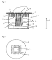
- the Fig. 1 1 shows a side view and in cross section of a chip ejector 1 according to the invention.
- the chip ejector 1 comprises a closed, vacuum-loadable chamber 2 with a preferably removable and exchangeable cover plate 3, on which a part of the film 4 rests with the semiconductor chips 5.
- the chamber 2 can also be formed by the housing of the chip ejector 1 or be a part thereof.
- the cover plate 3 may also be a lid.
- the cover plate 3 contains in the middle of a rectangular hole 6, which is about the same size as the semiconductor chips 5, and preferably a plurality of further holes 7, which only in the Fig. 2 are shown and serve to suck the film 4, when the chamber 2 is subjected to vacuum.
- the chip ejector 1 further comprises a plurality of plates 8, which are arranged in the interior of the chamber 2 next to each other and are jointly and / or individually displaceable in a direction referred to as z-direction.
- the z-direction as in the example preferably perpendicular to the surface 9 of the cover plate 3 or at least at an angle obliquely to the surface 9 of the cover 3, wherein the angle denotes the angle, the z-direction with the perpendicular to the surface 9 of the cover. 3 includes.
- the angle can be in a wide range from 0 to 80 ° and is usually limited only by the space available.
- the angle is clearly different from 90 °, since the scope of the invention is abandoned when the plates 8 are moved parallel to the surface 9 of the cover plate 3.
- the plates 8 protrude into the central hole 6 of the cover plate 3 and are advantageous to each other. Between the plates 8 and the edge of the hole 6 there is a circumferential gap 10.
- the chamber 2 can be acted upon with vacuum.
- the of the plates 8 within the hole 6 of the cover plate 3 of the chip ejector 1 ( Fig. 1 ) occupied surface is preferably slightly smaller than the surface of a semiconductor chip 5, namely so dimensioned that the semiconductor chip 5 projects beyond the area occupied by the plates 8 on all sides in the lateral direction by about 0.5 to 1 millimeters.
- the number of plates 8 depends on the dimensions of the semiconductor chip 5, it amounts to at least three, namely with very small semiconductor chips of 3 * 3 millimeters.
- plates means all objects that can perform the same function.
- the plates 8 can also be bars or bars.
- the plates, rods, beams, etc. abut each other or, if space permits, may also be separated by spacings.
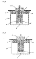
- the chip ejector 1 further comprises drive means to move the plates 8 together as well as individually in the z-direction.
- these drive means preferably comprise a first drive mechanism 11 and a second drive mechanism 12.
- the first drive mechanism 11 serves to displace all the plates 8 in the z-direction together and in this example also the second drive mechanism 12.
- the second drive mechanism 12 serves to shift the plates 8 individually in a predetermined order in the z-direction.
- the second drive mechanism 12 is formed based on the principle of the cam plate so that the plates 8 are positively displaced in the z-direction. This solution has the advantage that no springs are needed.
- the Fig. 2 shows the cover 3 of the chamber 2 of the chip ejector 1 in supervision.
- the lowering of the plates 8 in step C preferably begins either with one of the two outermost plates 8 ', 8 ", namely the outermost left plate 8' or the outermost right plate 8", or simultaneously with both outermost plates 8 'and 8 ".
- the lowering of the plates 8 can also begin with any other plate, the plates 8 are lowered by a second predetermined distance, and if the step BC is performed, then the second predetermined distance is greater than the first predetermined distance.
- the Fig. 1 shows a snapshot after step A.
- the Fig. 3 shows a snapshot after step BC.
- the Fig. 4 shows a snapshot at the time at which the two outermost plates 8 'and 8 "completely lowered and the plates adjacent to the outermost plates 8' and 8" are partially lowered.
- the film 4 has detached from the edge of the semiconductor chip 5.
- the Fig. 5 shows a snapshot at the time when already several of the plates 8 are completely lowered. The detachment of the film 4 from the semiconductor chip 5 is further advanced.
- the Fig. 6 11 shows a snapshot at the time at which all the plates 8, with the exception of a single plate 8 '' in the middle, are completely lowered, The plate 8 '' is already partly lowered and the foil 4 is completely detached from the semiconductor chip 5.
- the vacuum prevailing in the gap 10 exerts a suction force on the underside of the film 4 and pulls the film 4 towards the cover plate 3 of the chip ejector 1, so that the film 4 during the process step BC, if this is carried out, and during the process step C increasingly dissolves from the semiconductor chip 5 and is completed at the latest with the method step D.
- the support of the chip gripper 15 is required for the detachment of the film 4 from the semiconductor chip 5 depends on several factors, such as the thickness of the semiconductor chips 5, the size of the semiconductor chips 5, the adhesion of the film 4, the vacuum on the Slide 4 applied suction. The later the chip gripper 15 must be used, the greater the throughput of the automatic assembly machine.
- the drive means of the chip ejector 1 are selected such that the method step C or the method steps BC and C can be carried out in a very short time of typically less than 100 ms. This becomes possible when the plates 8 are forcibly guided.
- the preferred embodiment of the drive means with two drive mechanisms makes it possible to optimize the speed of the two process steps BC and C individually.
- the first drive mechanism 11 (FIG. Fig. 1 ) is, for example, a pneumatically movable cylinder, which can assume a first lowered and a second raised position.
- the first drive mechanism 11 may also be an electric drive whose z-position is programmatically adjustable.
- the second drive mechanism 12 is a cam-based mechanism.
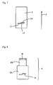
- the second drive mechanism 12 includes a motor 14 and a pin 13 movable along a predetermined path 17 that is reciprocated by the motor 14 between two end positions.
- the predetermined path 17 is preferably a straight line or a circular path.
- the plates 8 each contain a web-shaped opening 16 (FIG. Fig. 7 ) and the pin 13 is passed through all these openings.
- FIG. 7 shows one of the plates 8 with the web-shaped opening 16 and the guided through it pin 13 in supervision.
- the pin 13 is moved along the track 17, which in this example is a horizontal straight line, from the left end of the track 17 to the right end of the track 17, the disc 8 is moved in the negative z direction, namely the short one middle portion of the opening 16, which is inclined relative to the lateral sections. Because the pin 13 always occupies the same z-position in this embodiment, the plate 8 is lowered in the z-direction when the pin 13 passes through the central inclined portion. This central portion of the opening 16 is placed at a different location from plate 8 to plate 8 so that the plates 8 are lowered in a predetermined order in the z-direction as desired. If the pin 13 is moved not on a straight line, but on a circular path, then the web-shaped openings 16 have a correspondingly different course.
- the first drive mechanism 11 ( Fig. 1 ) to integrate to be effected movement in the second drive mechanism 12, so that the first drive mechanism 11 can be omitted.
- the web-shaped openings 16 of the plates 8 are provided with an additional portion which causes the simultaneous elevation of the plates 8 in the z-direction by a predetermined distance.
- the plates 8, as in the Fig. 8 illustrated preferably made in two parts, namely with a lower part 8A, which includes the web-shaped opening 16, and an upper part 8B, which is attachable to the lower part 8A.
- the lower parts 8A of the plates 8 remain unchanged in the chip ejector 1, while the number and width B of the upper parts 8B of the plates 8 and the hole 6 in the cover plate 3 are adapted to the dimensions of the semiconductor chip.
Landscapes
- Engineering & Computer Science (AREA)
- Physics & Mathematics (AREA)
- Condensed Matter Physics & Semiconductors (AREA)
- General Physics & Mathematics (AREA)
- Manufacturing & Machinery (AREA)
- Computer Hardware Design (AREA)
- Microelectronics & Electronic Packaging (AREA)
- Power Engineering (AREA)
- Container, Conveyance, Adherence, Positioning, Of Wafer (AREA)
- Moulds For Moulding Plastics Or The Like (AREA)
- Blow-Moulding Or Thermoforming Of Plastics Or The Like (AREA)
- Die Bonding (AREA)
Applications Claiming Priority (2)
| Application Number | Priority Date | Filing Date | Title |
|---|---|---|---|
| CH01748/08A CH699851A1 (de) | 2008-11-05 | 2008-11-05 | Chip-Auswerfer und Verfahren zum Ablösen und Entnehmen eines Halbleiterchips von einer Folie. |
| CH14522009 | 2009-09-18 |
Publications (2)
| Publication Number | Publication Date |
|---|---|
| EP2184765A1 EP2184765A1 (de) | 2010-05-12 |
| EP2184765B1 true EP2184765B1 (de) | 2011-12-14 |
Family
ID=41510771
Family Applications (1)
| Application Number | Title | Priority Date | Filing Date |
|---|---|---|---|
| EP09173469A Not-in-force EP2184765B1 (de) | 2008-11-05 | 2009-10-20 | Chip-Auswerfer |
Country Status (9)
Families Citing this family (22)
| Publication number | Priority date | Publication date | Assignee | Title |
|---|---|---|---|---|
| CN102376613B (zh) * | 2010-08-20 | 2013-04-03 | 吴华 | 集成电路装片机顶针模块 |
| DE112012003973T5 (de) * | 2011-09-22 | 2014-07-10 | Plus Seiki Co., Ltd | Vorrichtung zur Änderung der Abstände in einem Stapel |
| CH706280B1 (de) * | 2012-03-30 | 2016-03-15 | Esec Ag | Verfahren zum Ablösen eines Halbleiterchips von einer Folie. |
| KR101397750B1 (ko) * | 2012-07-25 | 2014-05-21 | 삼성전기주식회사 | 칩 이젝터 및 이를 이용한 칩 탈착 방법 |
| CH707236B1 (de) | 2012-11-23 | 2016-10-31 | Besi Switzerland Ag | Verfahren zum Ablösen von Halbleiterchips von einer Folie. |
| KR101957959B1 (ko) * | 2012-12-31 | 2019-03-13 | 세메스 주식회사 | 다이 이젝팅 방법 및 장치 |
| JP5717910B1 (ja) * | 2014-02-26 | 2015-05-13 | 株式会社新川 | 半導体ダイのピックアップ装置及びピックアップ方法 |
| SG10201403372SA (en) * | 2014-06-18 | 2016-01-28 | Mfg Integration Technology Ltd | System and method for peeling a semiconductor chip from a tape using a multistage ejector |
| JP6539336B2 (ja) * | 2015-03-23 | 2019-07-03 | リンテック株式会社 | 半導体加工用シートおよび半導体装置の製造方法 |
| JP6621771B2 (ja) * | 2017-01-25 | 2019-12-18 | ファスフォードテクノロジ株式会社 | 半導体製造装置および半導体装置の製造方法 |
| WO2019017584A1 (ko) * | 2017-07-18 | 2019-01-24 | 주식회사 루멘스 | 발광다이오드 모듈 제조 장치 및 방법 |
| JP7096261B2 (ja) * | 2017-07-18 | 2022-07-05 | ルーメンス カンパニー リミテッド | 発光ダイオードモジュール製造装置及び方法 |
| KR102380971B1 (ko) * | 2017-07-18 | 2022-04-01 | 주식회사 루멘스 | 발광다이오드 모듈 제조 장치 및 방법 |
| CN107920428B (zh) * | 2017-11-21 | 2023-06-30 | 南京工程学院 | 一种集成电路易拔ic底座 |
| TWI641070B (zh) * | 2018-01-09 | 2018-11-11 | 力成科技股份有限公司 | 晶片頂針裝置 |
| KR102617347B1 (ko) | 2018-10-04 | 2023-12-26 | 삼성전자주식회사 | 다이 이젝터 및 상기 다이 이젝터를 포함하는 다이 공급 장치 |
| CH715447B1 (de) | 2018-10-15 | 2022-01-14 | Besi Switzerland Ag | Chip-Auswerfer. |
| PL3739619T3 (pl) * | 2019-05-17 | 2022-10-17 | SR-Schindler Maschinen - Anlagentechnik GmbH | Instalacja do wytwarzania płyt z mechanizmem wyrzucającym |
| KR102220340B1 (ko) * | 2019-06-11 | 2021-02-25 | 세메스 주식회사 | 다이 이젝팅 장치 |
| KR102617784B1 (ko) * | 2020-07-09 | 2023-12-26 | 세메스 주식회사 | 다이 이젝터 및 이를 포함하는 다이 본딩 장치 |
| US11764098B2 (en) * | 2021-04-16 | 2023-09-19 | Asmpt Singapore Pte. Ltd. | Detaching a die from an adhesive tape by air ejection |
| JP7645768B2 (ja) * | 2021-10-26 | 2025-03-14 | 三菱電機株式会社 | 半導体製造装置および半導体装置の製造方法 |
Family Cites Families (19)
| Publication number | Priority date | Publication date | Assignee | Title |
|---|---|---|---|---|
| US4921564A (en) | 1988-05-23 | 1990-05-01 | Semiconductor Equipment Corp. | Method and apparatus for removing circuit chips from wafer handling tape |
| JP3498877B2 (ja) * | 1995-12-05 | 2004-02-23 | 株式会社東芝 | 半導体製造装置および半導体装置の製造方法 |
| JP2990197B1 (ja) * | 1999-01-20 | 1999-12-13 | 熊本日本電気株式会社 | 半導体チップのピックアップ装置 |
| JP2000353710A (ja) * | 1999-06-14 | 2000-12-19 | Toshiba Corp | ペレットピックアップ装置および半導体装置の製造方法 |
| JP3209736B2 (ja) | 1999-11-09 | 2001-09-17 | エヌイーシーマシナリー株式会社 | ペレットピックアップ装置 |
| JP4482243B2 (ja) | 2001-03-13 | 2010-06-16 | 株式会社新川 | ダイのピックアップ方法及びピックアップ装置 |
| US6889427B2 (en) * | 2002-02-15 | 2005-05-10 | Freescale Semiconductor, Inc. | Process for disengaging semiconductor die from an adhesive film |
| TWI225279B (en) | 2002-03-11 | 2004-12-11 | Hitachi Ltd | Semiconductor device and its manufacturing method |
| TW200414992A (en) * | 2002-11-29 | 2004-08-16 | Esec Trading Sa | Method for picking semiconductor chips from a foil |
| JP4574251B2 (ja) | 2003-09-17 | 2010-11-04 | ルネサスエレクトロニクス株式会社 | 半導体装置の製造方法 |
| EP1587138B1 (de) | 2004-04-13 | 2007-05-30 | Oerlikon Assembly Equipment AG, Steinhausen | Einrichtung für die Montage von Halbleiterchips und Verfahren zum Ablösen eines Halbleiterchips von einer Folie |
| CN100428402C (zh) * | 2004-04-13 | 2008-10-22 | 优利讯国际贸易有限责任公司 | 从箔片分离半导体芯片的方法和用于安装半导体芯片的设备 |
| US7240422B2 (en) * | 2004-05-11 | 2007-07-10 | Asm Assembly Automation Ltd. | Apparatus for semiconductor chip detachment |
| CH697213A5 (de) | 2004-05-19 | 2008-06-25 | Alphasem Ag | Verfahren und Vorrichtung zum Ablösen eines auf eine flexible Folie geklebten Bauteils. |
| US7303647B2 (en) * | 2004-10-29 | 2007-12-04 | Asm Assembly Automation Ltd. | Driving mechanism for chip detachment apparatus |
| US7665204B2 (en) | 2006-10-16 | 2010-02-23 | Asm Assembly Automation Ltd. | Die detachment apparatus comprising pre-peeling structure |
| JP2008141068A (ja) * | 2006-12-04 | 2008-06-19 | Shibaura Mechatronics Corp | 半導体チップのピックアップ装置及びピックアップ方法 |
| JP2008192736A (ja) * | 2007-02-02 | 2008-08-21 | Shibaura Mechatronics Corp | チップ実装装置、半導体ウエハ加工用粘着シート、およびチップ実装方法 |
| CN201084714Y (zh) * | 2007-10-16 | 2008-07-09 | 陈栋栋 | 芯片分离设备 |
-
2009
- 2009-10-07 MY MYPI20094184 patent/MY150953A/en unknown
- 2009-10-19 SG SG200906944-4A patent/SG161178A1/en unknown
- 2009-10-20 EP EP09173469A patent/EP2184765B1/de not_active Not-in-force
- 2009-10-20 AT AT09173469T patent/ATE537553T1/de active
- 2009-10-26 JP JP2009245745A patent/JP5488966B2/ja not_active Expired - Fee Related
- 2009-11-03 TW TW98137213A patent/TWI469241B/zh not_active IP Right Cessation
- 2009-11-03 US US12/611,758 patent/US8250742B2/en active Active
- 2009-11-04 KR KR1020090106216A patent/KR101612034B1/ko not_active Expired - Fee Related
- 2009-11-05 CN CN2009102118191A patent/CN101740349B/zh not_active Expired - Fee Related
Also Published As
| Publication number | Publication date |
|---|---|
| KR101612034B1 (ko) | 2016-04-12 |
| CN101740349B (zh) | 2013-09-25 |
| KR20100050432A (ko) | 2010-05-13 |
| SG161178A1 (en) | 2010-05-27 |
| US20100107405A1 (en) | 2010-05-06 |
| ATE537553T1 (de) | 2011-12-15 |
| JP2010114441A (ja) | 2010-05-20 |
| TW201025483A (en) | 2010-07-01 |
| CN101740349A (zh) | 2010-06-16 |
| JP5488966B2 (ja) | 2014-05-14 |
| MY150953A (en) | 2014-03-31 |
| US8250742B2 (en) | 2012-08-28 |
| EP2184765A1 (de) | 2010-05-12 |
| TWI469241B (zh) | 2015-01-11 |
Similar Documents
| Publication | Publication Date | Title |
|---|---|---|
| EP2184765B1 (de) | Chip-Auswerfer | |
| DE112009000200B4 (de) | Betätigungsvorrichtungen für eine Vorrichtung und ein Verfahren zum Ausrichten und Halten einer Mehrzahl singulierter Halbleiterbauelemente in Aufnahmetaschen eines Klemmträgers | |
| DE102013103100B4 (de) | Verfahren zum Ablösen eines Halbleiterchips von einer Folie | |
| DE2858098C2 (de) | Vorrichtung zum Aufbringen von rechteckigen oder länglichen Chips auf eine Leiterplatte | |
| DE10349847B3 (de) | Positionierungsvorrichtung und -Verfahren für die Übertragung elektronischer Bauteile | |
| DE102017205095B3 (de) | Vorrichtung und Verfahren zum Entnehmen eines Werkstückteils aus einem Restwerkstück | |
| DE2028910C3 (de) | Einrichtung zum Sortieren von elektrischen Schaltungselementen | |
| DE2653707C3 (de) | Vorrichtung zum genauen visuell- manuellen Einrichten und zum Halten eines plattenförmigen Werkstücks mit lichtempfindlicher Schicht gegenüber einer oder zwei Vorlagen | |
| EP2359398B1 (de) | Verfahren zum ablösen und entnehmen eines halbleiterchips von einer folie | |
| CH697146A5 (de) | Greifvorrichtung zur Handhabung von Wafern. | |
| EP1587138B1 (de) | Einrichtung für die Montage von Halbleiterchips und Verfahren zum Ablösen eines Halbleiterchips von einer Folie | |
| EP2842654A1 (de) | Vorrichtung und Verfahren zum Transfer von Werkstücken in und aus einem Werkzeug | |
| CH697213A5 (de) | Verfahren und Vorrichtung zum Ablösen eines auf eine flexible Folie geklebten Bauteils. | |
| EP0002496B1 (de) | Verfahren und Vorrichtung zum Ausrichten flacher dünner Werkstücke | |
| DE102006025361A1 (de) | Ausstoßeinheit zum Abtrennen von Bauelementen aus einer im Wesentlichen ebenen Anordnung von Bauelementen | |
| CH699851A1 (de) | Chip-Auswerfer und Verfahren zum Ablösen und Entnehmen eines Halbleiterchips von einer Folie. | |
| EP3443587B1 (de) | Vorrichtung, system und verfahren zum ausrichten elektronischer bauteile | |
| DE68918823T2 (de) | Vorrichtung zum Ausschneiden von Tab-Anordnungen und zum Formen von deren Anschlüssen. | |
| DE102008064166A1 (de) | Automatisierte Werkzeugmaschine und Verfahren zum Einbringen von Referenzbohrungen in Leiterplatten | |
| DE19646186A1 (de) | Vorrichtung zum Halten einer Leiterplatte | |
| DE10222620A1 (de) | Verfahren zum Verarbeiten von elektrischen Bauteilen, insbesondere zum Verarbeiten von Halbleiterchips sowie elektrischen Bauelementen, sowie Vorrichtung zum Durchführen des Verfahrens | |
| EP1304726B1 (de) | Anordnung und Verfahren zur Aufnahme und zum Bearbeiten eines dünnen Wafers | |
| DE69016631T2 (de) | Vorrichtung zum Laden und Entladen einer Speicherkassette mit flachen Gegenständen. | |
| DE2048079A1 (de) | Verfahren und Vorrichtung zum Kontak tieren | |
| DE60033259T2 (de) | Einrichtung zum Befördern und Halten von plattenförmigem Material |
Legal Events
| Date | Code | Title | Description |
|---|---|---|---|
| PUAI | Public reference made under article 153(3) epc to a published international application that has entered the european phase |
Free format text: ORIGINAL CODE: 0009012 |
|
| AK | Designated contracting states |
Kind code of ref document: A1 Designated state(s): AT BE BG CH CY CZ DE DK EE ES FI FR GB GR HR HU IE IS IT LI LT LU LV MC MK MT NL NO PL PT RO SE SI SK SM TR |
|
| AX | Request for extension of the european patent |
Extension state: AL BA RS |
|
| 17P | Request for examination filed |
Effective date: 20101112 |
|
| RIC1 | Information provided on ipc code assigned before grant |
Ipc: H01L 21/00 20060101AFI20110524BHEP |
|
| GRAP | Despatch of communication of intention to grant a patent |
Free format text: ORIGINAL CODE: EPIDOSNIGR1 |
|
| GRAS | Grant fee paid |
Free format text: ORIGINAL CODE: EPIDOSNIGR3 |
|
| GRAA | (expected) grant |
Free format text: ORIGINAL CODE: 0009210 |
|
| AK | Designated contracting states |
Kind code of ref document: B1 Designated state(s): AT BE BG CH CY CZ DE DK EE ES FI FR GB GR HR HU IE IS IT LI LT LU LV MC MK MT NL NO PL PT RO SE SI SK SM TR |
|
| REG | Reference to a national code |
Ref country code: GB Ref legal event code: FG4D Free format text: NOT ENGLISH |
|
| REG | Reference to a national code |
Ref country code: CH Ref legal event code: EP |
|
| REG | Reference to a national code |
Ref country code: IE Ref legal event code: FG4D |
|
| REG | Reference to a national code |
Ref country code: DE Ref legal event code: R096 Ref document number: 502009002190 Country of ref document: DE Effective date: 20120209 |
|
| REG | Reference to a national code |
Ref country code: NL Ref legal event code: VDEP Effective date: 20111214 |
|
| PG25 | Lapsed in a contracting state [announced via postgrant information from national office to epo] |
Ref country code: NO Free format text: LAPSE BECAUSE OF FAILURE TO SUBMIT A TRANSLATION OF THE DESCRIPTION OR TO PAY THE FEE WITHIN THE PRESCRIBED TIME-LIMIT Effective date: 20120314 Ref country code: LT Free format text: LAPSE BECAUSE OF FAILURE TO SUBMIT A TRANSLATION OF THE DESCRIPTION OR TO PAY THE FEE WITHIN THE PRESCRIBED TIME-LIMIT Effective date: 20111214 |
|
| LTIE | Lt: invalidation of european patent or patent extension |
Effective date: 20111214 |
|
| PG25 | Lapsed in a contracting state [announced via postgrant information from national office to epo] |
Ref country code: SI Free format text: LAPSE BECAUSE OF FAILURE TO SUBMIT A TRANSLATION OF THE DESCRIPTION OR TO PAY THE FEE WITHIN THE PRESCRIBED TIME-LIMIT Effective date: 20111214 Ref country code: SE Free format text: LAPSE BECAUSE OF FAILURE TO SUBMIT A TRANSLATION OF THE DESCRIPTION OR TO PAY THE FEE WITHIN THE PRESCRIBED TIME-LIMIT Effective date: 20111214 Ref country code: GR Free format text: LAPSE BECAUSE OF FAILURE TO SUBMIT A TRANSLATION OF THE DESCRIPTION OR TO PAY THE FEE WITHIN THE PRESCRIBED TIME-LIMIT Effective date: 20120315 Ref country code: NL Free format text: LAPSE BECAUSE OF FAILURE TO SUBMIT A TRANSLATION OF THE DESCRIPTION OR TO PAY THE FEE WITHIN THE PRESCRIBED TIME-LIMIT Effective date: 20111214 Ref country code: HR Free format text: LAPSE BECAUSE OF FAILURE TO SUBMIT A TRANSLATION OF THE DESCRIPTION OR TO PAY THE FEE WITHIN THE PRESCRIBED TIME-LIMIT Effective date: 20111214 Ref country code: LV Free format text: LAPSE BECAUSE OF FAILURE TO SUBMIT A TRANSLATION OF THE DESCRIPTION OR TO PAY THE FEE WITHIN THE PRESCRIBED TIME-LIMIT Effective date: 20111214 |
|
| PG25 | Lapsed in a contracting state [announced via postgrant information from national office to epo] |
Ref country code: CY Free format text: LAPSE BECAUSE OF FAILURE TO SUBMIT A TRANSLATION OF THE DESCRIPTION OR TO PAY THE FEE WITHIN THE PRESCRIBED TIME-LIMIT Effective date: 20111214 |
|
| REG | Reference to a national code |
Ref country code: IE Ref legal event code: FD4D |
|
| PG25 | Lapsed in a contracting state [announced via postgrant information from national office to epo] |
Ref country code: IS Free format text: LAPSE BECAUSE OF FAILURE TO SUBMIT A TRANSLATION OF THE DESCRIPTION OR TO PAY THE FEE WITHIN THE PRESCRIBED TIME-LIMIT Effective date: 20120414 Ref country code: BG Free format text: LAPSE BECAUSE OF FAILURE TO SUBMIT A TRANSLATION OF THE DESCRIPTION OR TO PAY THE FEE WITHIN THE PRESCRIBED TIME-LIMIT Effective date: 20120314 Ref country code: EE Free format text: LAPSE BECAUSE OF FAILURE TO SUBMIT A TRANSLATION OF THE DESCRIPTION OR TO PAY THE FEE WITHIN THE PRESCRIBED TIME-LIMIT Effective date: 20111214 Ref country code: SK Free format text: LAPSE BECAUSE OF FAILURE TO SUBMIT A TRANSLATION OF THE DESCRIPTION OR TO PAY THE FEE WITHIN THE PRESCRIBED TIME-LIMIT Effective date: 20111214 Ref country code: IE Free format text: LAPSE BECAUSE OF FAILURE TO SUBMIT A TRANSLATION OF THE DESCRIPTION OR TO PAY THE FEE WITHIN THE PRESCRIBED TIME-LIMIT Effective date: 20111214 Ref country code: CZ Free format text: LAPSE BECAUSE OF FAILURE TO SUBMIT A TRANSLATION OF THE DESCRIPTION OR TO PAY THE FEE WITHIN THE PRESCRIBED TIME-LIMIT Effective date: 20111214 |
|
| PG25 | Lapsed in a contracting state [announced via postgrant information from national office to epo] |
Ref country code: PT Free format text: LAPSE BECAUSE OF FAILURE TO SUBMIT A TRANSLATION OF THE DESCRIPTION OR TO PAY THE FEE WITHIN THE PRESCRIBED TIME-LIMIT Effective date: 20120416 Ref country code: RO Free format text: LAPSE BECAUSE OF FAILURE TO SUBMIT A TRANSLATION OF THE DESCRIPTION OR TO PAY THE FEE WITHIN THE PRESCRIBED TIME-LIMIT Effective date: 20111214 Ref country code: PL Free format text: LAPSE BECAUSE OF FAILURE TO SUBMIT A TRANSLATION OF THE DESCRIPTION OR TO PAY THE FEE WITHIN THE PRESCRIBED TIME-LIMIT Effective date: 20111214 |
|
| PLBE | No opposition filed within time limit |
Free format text: ORIGINAL CODE: 0009261 |
|
| STAA | Information on the status of an ep patent application or granted ep patent |
Free format text: STATUS: NO OPPOSITION FILED WITHIN TIME LIMIT |
|
| PG25 | Lapsed in a contracting state [announced via postgrant information from national office to epo] |
Ref country code: DK Free format text: LAPSE BECAUSE OF FAILURE TO SUBMIT A TRANSLATION OF THE DESCRIPTION OR TO PAY THE FEE WITHIN THE PRESCRIBED TIME-LIMIT Effective date: 20111214 |
|
| 26N | No opposition filed |
Effective date: 20120917 |
|
| PG25 | Lapsed in a contracting state [announced via postgrant information from national office to epo] |
Ref country code: IT Free format text: LAPSE BECAUSE OF FAILURE TO SUBMIT A TRANSLATION OF THE DESCRIPTION OR TO PAY THE FEE WITHIN THE PRESCRIBED TIME-LIMIT Effective date: 20111214 |
|
| REG | Reference to a national code |
Ref country code: DE Ref legal event code: R097 Ref document number: 502009002190 Country of ref document: DE Effective date: 20120917 |
|
| BERE | Be: lapsed |
Owner name: ESEC A.G. Effective date: 20121031 |
|
| PG25 | Lapsed in a contracting state [announced via postgrant information from national office to epo] |
Ref country code: ES Free format text: LAPSE BECAUSE OF FAILURE TO SUBMIT A TRANSLATION OF THE DESCRIPTION OR TO PAY THE FEE WITHIN THE PRESCRIBED TIME-LIMIT Effective date: 20120325 |
|
| PG25 | Lapsed in a contracting state [announced via postgrant information from national office to epo] |
Ref country code: MC Free format text: LAPSE BECAUSE OF NON-PAYMENT OF DUE FEES Effective date: 20121031 |
|
| PG25 | Lapsed in a contracting state [announced via postgrant information from national office to epo] |
Ref country code: FI Free format text: LAPSE BECAUSE OF FAILURE TO SUBMIT A TRANSLATION OF THE DESCRIPTION OR TO PAY THE FEE WITHIN THE PRESCRIBED TIME-LIMIT Effective date: 20111214 |
|
| PG25 | Lapsed in a contracting state [announced via postgrant information from national office to epo] |
Ref country code: BE Free format text: LAPSE BECAUSE OF NON-PAYMENT OF DUE FEES Effective date: 20121031 |
|
| PG25 | Lapsed in a contracting state [announced via postgrant information from national office to epo] |
Ref country code: MT Free format text: LAPSE BECAUSE OF FAILURE TO SUBMIT A TRANSLATION OF THE DESCRIPTION OR TO PAY THE FEE WITHIN THE PRESCRIBED TIME-LIMIT Effective date: 20111214 |
|
| PG25 | Lapsed in a contracting state [announced via postgrant information from national office to epo] |
Ref country code: TR Free format text: LAPSE BECAUSE OF FAILURE TO SUBMIT A TRANSLATION OF THE DESCRIPTION OR TO PAY THE FEE WITHIN THE PRESCRIBED TIME-LIMIT Effective date: 20111214 |
|
| PG25 | Lapsed in a contracting state [announced via postgrant information from national office to epo] |
Ref country code: LU Free format text: LAPSE BECAUSE OF NON-PAYMENT OF DUE FEES Effective date: 20121020 Ref country code: SM Free format text: LAPSE BECAUSE OF FAILURE TO SUBMIT A TRANSLATION OF THE DESCRIPTION OR TO PAY THE FEE WITHIN THE PRESCRIBED TIME-LIMIT Effective date: 20111214 |
|
| GBPC | Gb: european patent ceased through non-payment of renewal fee |
Effective date: 20131020 |
|
| PG25 | Lapsed in a contracting state [announced via postgrant information from national office to epo] |
Ref country code: GB Free format text: LAPSE BECAUSE OF NON-PAYMENT OF DUE FEES Effective date: 20131020 Ref country code: HU Free format text: LAPSE BECAUSE OF FAILURE TO SUBMIT A TRANSLATION OF THE DESCRIPTION OR TO PAY THE FEE WITHIN THE PRESCRIBED TIME-LIMIT Effective date: 20091020 |
|
| PG25 | Lapsed in a contracting state [announced via postgrant information from national office to epo] |
Ref country code: MK Free format text: LAPSE BECAUSE OF FAILURE TO SUBMIT A TRANSLATION OF THE DESCRIPTION OR TO PAY THE FEE WITHIN THE PRESCRIBED TIME-LIMIT Effective date: 20111214 |
|
| REG | Reference to a national code |
Ref country code: AT Ref legal event code: MM01 Ref document number: 537553 Country of ref document: AT Kind code of ref document: T Effective date: 20141020 |
|
| PG25 | Lapsed in a contracting state [announced via postgrant information from national office to epo] |
Ref country code: AT Free format text: LAPSE BECAUSE OF NON-PAYMENT OF DUE FEES Effective date: 20141020 |
|
| REG | Reference to a national code |
Ref country code: FR Ref legal event code: PLFP Year of fee payment: 8 |
|
| REG | Reference to a national code |
Ref country code: FR Ref legal event code: PLFP Year of fee payment: 9 |
|
| REG | Reference to a national code |
Ref country code: FR Ref legal event code: PLFP Year of fee payment: 10 |
|
| REG | Reference to a national code |
Ref country code: CH Ref legal event code: NV Representative=s name: IP.DESIGN KANZLEI AND PATENTBUERO DR. MARC-TIM, CH Ref country code: CH Ref legal event code: PFA Owner name: BESI SWITZERLAND AG, CH Free format text: FORMER OWNER: ESEC AG, CH |
|
| REG | Reference to a national code |
Ref country code: CH Ref legal event code: PCAR Free format text: NEW ADDRESS: ARBONERSTRASSE 35, 8580 AMRISWIL (CH) |
|
| REG | Reference to a national code |
Ref country code: DE Ref legal event code: R081 Ref document number: 502009002190 Country of ref document: DE Owner name: BESI SWITZERLAND AG, CH Free format text: FORMER OWNER: ESEC AG, CHAM, CH |
|
| PGFP | Annual fee paid to national office [announced via postgrant information from national office to epo] |
Ref country code: CH Payment date: 20211101 Year of fee payment: 13 |
|
| PGFP | Annual fee paid to national office [announced via postgrant information from national office to epo] |
Ref country code: FR Payment date: 20221004 Year of fee payment: 14 |
|
| PGFP | Annual fee paid to national office [announced via postgrant information from national office to epo] |
Ref country code: DE Payment date: 20220610 Year of fee payment: 14 |
|
| REG | Reference to a national code |
Ref country code: CH Ref legal event code: PL |
|
| PG25 | Lapsed in a contracting state [announced via postgrant information from national office to epo] |
Ref country code: LI Free format text: LAPSE BECAUSE OF NON-PAYMENT OF DUE FEES Effective date: 20221031 Ref country code: CH Free format text: LAPSE BECAUSE OF NON-PAYMENT OF DUE FEES Effective date: 20221031 |
|
| REG | Reference to a national code |
Ref country code: DE Ref legal event code: R119 Ref document number: 502009002190 Country of ref document: DE |
|
| PG25 | Lapsed in a contracting state [announced via postgrant information from national office to epo] |
Ref country code: FR Free format text: LAPSE BECAUSE OF NON-PAYMENT OF DUE FEES Effective date: 20231031 Ref country code: DE Free format text: LAPSE BECAUSE OF NON-PAYMENT OF DUE FEES Effective date: 20240501 |