EP2175488A1 - Halbleiterbauelement und herstellungsverfahren dafür - Google Patents
Halbleiterbauelement und herstellungsverfahren dafür Download PDFInfo
- Publication number
- EP2175488A1 EP2175488A1 EP08790927A EP08790927A EP2175488A1 EP 2175488 A1 EP2175488 A1 EP 2175488A1 EP 08790927 A EP08790927 A EP 08790927A EP 08790927 A EP08790927 A EP 08790927A EP 2175488 A1 EP2175488 A1 EP 2175488A1
- Authority
- EP
- European Patent Office
- Prior art keywords
- layer
- metal layer
- semiconductor device
- metal
- disposed
- Prior art date
- Legal status (The legal status is an assumption and is not a legal conclusion. Google has not performed a legal analysis and makes no representation as to the accuracy of the status listed.)
- Withdrawn
Links
Images


Classifications
-
- H—ELECTRICITY
- H10—SEMICONDUCTOR DEVICES; ELECTRIC SOLID-STATE DEVICES NOT OTHERWISE PROVIDED FOR
- H10D—INORGANIC ELECTRIC SEMICONDUCTOR DEVICES
- H10D30/00—Field-effect transistors [FET]
- H10D30/60—Insulated-gate field-effect transistors [IGFET]
- H10D30/64—Double-diffused metal-oxide semiconductor [DMOS] FETs
- H10D30/66—Vertical DMOS [VDMOS] FETs
-
- H—ELECTRICITY
- H10—SEMICONDUCTOR DEVICES; ELECTRIC SOLID-STATE DEVICES NOT OTHERWISE PROVIDED FOR
- H10D—INORGANIC ELECTRIC SEMICONDUCTOR DEVICES
- H10D30/00—Field-effect transistors [FET]
- H10D30/01—Manufacture or treatment
- H10D30/021—Manufacture or treatment of FETs having insulated gates [IGFET]
- H10D30/025—Manufacture or treatment of FETs having insulated gates [IGFET] of vertical IGFETs
-
- H—ELECTRICITY
- H10—SEMICONDUCTOR DEVICES; ELECTRIC SOLID-STATE DEVICES NOT OTHERWISE PROVIDED FOR
- H10D—INORGANIC ELECTRIC SEMICONDUCTOR DEVICES
- H10D30/00—Field-effect transistors [FET]
- H10D30/01—Manufacture or treatment
- H10D30/021—Manufacture or treatment of FETs having insulated gates [IGFET]
- H10D30/028—Manufacture or treatment of FETs having insulated gates [IGFET] of double-diffused metal oxide semiconductor [DMOS] FETs
- H10D30/0291—Manufacture or treatment of FETs having insulated gates [IGFET] of double-diffused metal oxide semiconductor [DMOS] FETs of vertical DMOS [VDMOS] FETs
-
- H—ELECTRICITY
- H10—SEMICONDUCTOR DEVICES; ELECTRIC SOLID-STATE DEVICES NOT OTHERWISE PROVIDED FOR
- H10D—INORGANIC ELECTRIC SEMICONDUCTOR DEVICES
- H10D64/00—Electrodes of devices having potential barriers
- H10D64/60—Electrodes characterised by their materials
- H10D64/64—Electrodes comprising a Schottky barrier to a semiconductor
-
- H—ELECTRICITY
- H10—SEMICONDUCTOR DEVICES; ELECTRIC SOLID-STATE DEVICES NOT OTHERWISE PROVIDED FOR
- H10D—INORGANIC ELECTRIC SEMICONDUCTOR DEVICES
- H10D8/00—Diodes
- H10D8/01—Manufacture or treatment
- H10D8/051—Manufacture or treatment of Schottky diodes
-
- H—ELECTRICITY
- H10—SEMICONDUCTOR DEVICES; ELECTRIC SOLID-STATE DEVICES NOT OTHERWISE PROVIDED FOR
- H10D—INORGANIC ELECTRIC SEMICONDUCTOR DEVICES
- H10D84/00—Integrated devices formed in or on semiconductor substrates that comprise only semiconducting layers, e.g. on Si wafers or on GaAs-on-Si wafers
- H10D84/101—Integrated devices comprising main components and built-in components, e.g. IGBT having built-in freewheel diode
- H10D84/141—VDMOS having built-in components
- H10D84/146—VDMOS having built-in components the built-in components being Schottky barrier diodes
-
- H—ELECTRICITY
- H10—SEMICONDUCTOR DEVICES; ELECTRIC SOLID-STATE DEVICES NOT OTHERWISE PROVIDED FOR
- H10D—INORGANIC ELECTRIC SEMICONDUCTOR DEVICES
- H10D84/00—Integrated devices formed in or on semiconductor substrates that comprise only semiconducting layers, e.g. on Si wafers or on GaAs-on-Si wafers
- H10D84/80—Integrated devices formed in or on semiconductor substrates that comprise only semiconducting layers, e.g. on Si wafers or on GaAs-on-Si wafers characterised by the integration of at least one component covered by groups H10D12/00 or H10D30/00, e.g. integration of IGFETs
- H10D84/811—Combinations of field-effect devices and one or more diodes, capacitors or resistors
-
- H—ELECTRICITY
- H10—SEMICONDUCTOR DEVICES; ELECTRIC SOLID-STATE DEVICES NOT OTHERWISE PROVIDED FOR
- H10D—INORGANIC ELECTRIC SEMICONDUCTOR DEVICES
- H10D89/00—Aspects of integrated devices not covered by groups H10D84/00 - H10D88/00
- H10D89/60—Integrated devices comprising arrangements for electrical or thermal protection, e.g. protection circuits against electrostatic discharge [ESD]
- H10D89/601—Integrated devices comprising arrangements for electrical or thermal protection, e.g. protection circuits against electrostatic discharge [ESD] for devices having insulated gate electrodes, e.g. for IGFETs or IGBTs
- H10D89/611—Integrated devices comprising arrangements for electrical or thermal protection, e.g. protection circuits against electrostatic discharge [ESD] for devices having insulated gate electrodes, e.g. for IGFETs or IGBTs using diodes as protective elements
-
- H—ELECTRICITY
- H10—SEMICONDUCTOR DEVICES; ELECTRIC SOLID-STATE DEVICES NOT OTHERWISE PROVIDED FOR
- H10P—GENERIC PROCESSES OR APPARATUS FOR THE MANUFACTURE OR TREATMENT OF DEVICES COVERED BY CLASS H10
- H10P14/00—Formation of materials, e.g. in the shape of layers or pillars
- H10P14/40—Formation of materials, e.g. in the shape of layers or pillars of conductive or resistive materials
-
- G—PHYSICS
- G09—EDUCATION; CRYPTOGRAPHY; DISPLAY; ADVERTISING; SEALS
- G09G—ARRANGEMENTS OR CIRCUITS FOR CONTROL OF INDICATING DEVICES USING STATIC MEANS TO PRESENT VARIABLE INFORMATION
- G09G3/00—Control arrangements or circuits, of interest only in connection with visual indicators other than cathode-ray tubes
- G09G3/20—Control arrangements or circuits, of interest only in connection with visual indicators other than cathode-ray tubes for presentation of an assembly of a number of characters, e.g. a page, by composing the assembly by combination of individual elements arranged in a matrix no fixed position being assigned to or needed to be assigned to the individual characters or partial characters
- G09G3/34—Control arrangements or circuits, of interest only in connection with visual indicators other than cathode-ray tubes for presentation of an assembly of a number of characters, e.g. a page, by composing the assembly by combination of individual elements arranged in a matrix no fixed position being assigned to or needed to be assigned to the individual characters or partial characters by control of light from an independent source
Definitions
- n channel vertical MOSFET Metal Oxide Semiconductor Field Effect Transistor
- LCD Liquid Crystal Display
- inverter power circuit of various kinds of air-conditioners an inverter power circuit for driving various kinds of lighting devices, etc.
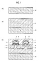
- a semiconductor device comprising an insulated gate field effect transistor comprising a semiconductor substrate having a first conductivity type and forming a drain layer, a base layer disposed on a surface of the semiconductor substrate and having a second conductivity type, a source layer disposed on the base layer and having the first conductivity type, a gate insulating film disposed on the semiconductor substrate, the base layer, and the source layer, a gate electrode disposed on the gate insulating film, and a source electrode connected to the base layer and the source layer; and a metal laminate structure comprising a second metal layer disposed on a first metal layer disposed on a back side of the semiconductor substrate and subjected to an alloy process with the semiconductor substrate, a third metal layer disposed on the second metal layer, and a fourth metal layer disposed on the third metal layer, wherein the semiconductor device includes a Schottky diode applying the metal laminate structure as an anode, and applying the semiconductor substrate as a cathode.
- the semiconductor device according to the first embodiment forms the first Au layer on the n type silicon semiconductor substrate 10 as the metal layer 11 which is not doped with the impurities, such as Sb and As, and, after an alloy process with the n + type silicon semiconductor substrate 10, forms the metal laminate structure 20 including the metal layer 12 composed of the Ti layer or Cr layer for an assembly, the metal layer 14 composed of a Ni layer, and the metal layer 16 composed of the second Au layer.
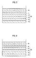
- the configuration of the metal laminate structure 20 is only differing from the semiconductor device according to the semiconductor device according to the first embodiment, and other configurations are the same as that of the semiconductor device according to the first embodiment. That is, as shown in Fig.
- the n type epitaxial growth layer 8 is formed on the n + type silicon semiconductor substrate 10.
- the impurity concentration is about 1 ⁇ 10 15 to 10 17 cm -3 , for example.
- the p type base layer 6 and the n type source layer 4 is formed by an ion implantation technology after patterning the gate insulating film 2 and the gate electrode 3.
- the ion such as B, Al, Ga, or In, etc.
- the impurity ion for forming the p type base layer 6.
- the ion such as P, As, Sb, or Bi, etc.
- the accelerating energy and the amount of dosage can be determined according to the diffusing depth and the impurity concentration profile of the each layer.
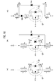
- a Schottky diode is formed by disposing the metal laminate structure 20 on the n + type silicon semiconductor substrate 10, in the rear electrode configuration at the drain side of the n channel vertical MOSFET.
- the Schottky diode is an SBD connected to the drain layer of the n channel vertical MOSFET.
- the cathode of the Schottky diode is connected to the drain of the vertical MOSFET, and the anode of the Schottky diode is connected to the drain terminal D.
- the source of the vertical MOSFET is connected to the source terminal S.
- the metal layer 11 composed of the Au layer is formed on the n + silicon semiconductor substrate 10, and the n + silicon semiconductor substrate 10 and the metal layer 11 are subjected to the alloy process, as shown in Fig. 9(b) . Furthermore, the metal laminate structure 20 is provided on the metal layer 11.
- the metal laminate structure 20 includes various kinds of structural examples as shown in Fig. 3 to Fig. 6 , for example.
- the semiconductor device of the present invention can be applied to a back light inverter circuit of an LCD (liquid crystal display), an inverter circuit for air-conditioners, and an inverter circuit for driving a lighting device, and is available in whole of n channel vertical MOSFET.
- LCD liquid crystal display
- inverter circuit for air-conditioners and an inverter circuit for driving a lighting device, and is available in whole of n channel vertical MOSFET.
Landscapes
- Electrodes Of Semiconductors (AREA)
- Thin Film Transistor (AREA)
Applications Claiming Priority (2)
| Application Number | Priority Date | Filing Date | Title |
|---|---|---|---|
| JP2007199122 | 2007-07-31 | ||
| PCT/JP2008/062266 WO2009016928A1 (ja) | 2007-07-31 | 2008-07-07 | 半導体装置およびその製造方法 |
Publications (2)
| Publication Number | Publication Date |
|---|---|
| EP2175488A1 true EP2175488A1 (de) | 2010-04-14 |
| EP2175488A4 EP2175488A4 (de) | 2010-12-08 |
Family
ID=40304165
Family Applications (1)
| Application Number | Title | Priority Date | Filing Date |
|---|---|---|---|
| EP08790927A Withdrawn EP2175488A4 (de) | 2007-07-31 | 2008-07-07 | Halbleiterbauelement und herstellungsverfahren dafür |
Country Status (4)
| Country | Link |
|---|---|
| US (2) | US20110284948A1 (de) |
| EP (1) | EP2175488A4 (de) |
| JP (1) | JP5460320B2 (de) |
| WO (1) | WO2009016928A1 (de) |
Families Citing this family (4)
| Publication number | Priority date | Publication date | Assignee | Title |
|---|---|---|---|---|
| DE102009059303A1 (de) * | 2009-12-23 | 2011-06-30 | United Monolithic Semiconductors GmbH, 89081 | Verfahren zur Herstellung eines elektronischen Bauteils und nach diesem Verfahren hergestelltes elektronisches Bauteil |
| JP6335717B2 (ja) * | 2014-08-20 | 2018-05-30 | 昭和電工株式会社 | 半導体デバイス |
| TWI658568B (zh) * | 2017-01-03 | 2019-05-01 | Leadtrend Technology Corporation | 高壓半導體元件以及同步整流控制器 |
| CN108305872B (zh) * | 2017-01-12 | 2020-12-11 | 通嘉科技股份有限公司 | 高压半导体元件以及同步整流控制器 |
Family Cites Families (22)
| Publication number | Priority date | Publication date | Assignee | Title |
|---|---|---|---|---|
| JPS5799785A (en) * | 1980-12-11 | 1982-06-21 | Mitsubishi Electric Corp | Schottky barrier diode |
| US4811065A (en) * | 1987-06-11 | 1989-03-07 | Siliconix Incorporated | Power DMOS transistor with high speed body diode |
| US5273917A (en) | 1989-08-19 | 1993-12-28 | Fuji Electric Co., Ltd. | Method for manufacturing a conductivity modulation MOSFET |
| JPH03155677A (ja) * | 1989-08-19 | 1991-07-03 | Fuji Electric Co Ltd | 伝導度変調型mosfet |
| JPH08148675A (ja) * | 1994-11-15 | 1996-06-07 | Fuji Electric Co Ltd | 半導体装置 |
| US5589408A (en) | 1995-07-05 | 1996-12-31 | Motorola, Inc. | Method of forming an alloyed drain field effect transistor and device formed |
| JPH10173166A (ja) * | 1996-12-05 | 1998-06-26 | Murata Mfg Co Ltd | 電界効果トランジスタ及びその製造方法 |
| JP3684729B2 (ja) * | 1996-12-16 | 2005-08-17 | 株式会社村田製作所 | ショットキー接合半導体装置の製造方法 |
| JPH10178190A (ja) * | 1996-12-16 | 1998-06-30 | Murata Mfg Co Ltd | 半導体装置の製造方法 |
| JP2950285B2 (ja) * | 1997-05-07 | 1999-09-20 | サンケン電気株式会社 | 半導体素子及びその電極の形成方法 |
| JPH11135512A (ja) * | 1997-10-31 | 1999-05-21 | Mitsubishi Electric Corp | 電力用半導体装置及びその製造方法 |
| JP2001135814A (ja) * | 1999-11-02 | 2001-05-18 | Shindengen Electric Mfg Co Ltd | 縦型mos電界効果トランジスタ |
| DE10015884A1 (de) * | 2000-03-30 | 2001-10-11 | Philips Corp Intellectual Pty | Schottky-Diode |
| US6504208B2 (en) * | 2001-02-27 | 2003-01-07 | International Business Machines Corporation | Power MOSFET device, structures employing the same and methods of fabrication |
| JP2003324197A (ja) * | 2002-04-30 | 2003-11-14 | Rohm Co Ltd | 半導体装置およびその製造方法 |
| JP2004303755A (ja) * | 2003-03-28 | 2004-10-28 | Renesas Technology Corp | 半導体装置の製造方法および半導体装置 |
| JP4917246B2 (ja) * | 2003-11-17 | 2012-04-18 | ローム株式会社 | 半導体装置およびその製造方法 |
| JP4622447B2 (ja) * | 2004-01-23 | 2011-02-02 | 住友電気工業株式会社 | Iii族窒化物結晶基板の製造方法 |
| US20050242411A1 (en) | 2004-04-29 | 2005-11-03 | Hsuan Tso | [superjunction schottky device and fabrication thereof] |
| JP2006202931A (ja) * | 2005-01-20 | 2006-08-03 | Renesas Technology Corp | 半導体装置およびその製造方法 |
| JP2007123395A (ja) * | 2005-10-26 | 2007-05-17 | Renesas Technology Corp | 半導体装置および半導体装置の製造方法 |
| US7659191B2 (en) * | 2006-11-27 | 2010-02-09 | Alpha And Omega Semiconductor Incorporated | Gold/silicon eutectic die bonding method |
-
2007
- 2007-07-07 US US12/671,581 patent/US20110284948A1/en not_active Abandoned
-
2008
- 2008-07-07 JP JP2009525323A patent/JP5460320B2/ja not_active Expired - Fee Related
- 2008-07-07 WO PCT/JP2008/062266 patent/WO2009016928A1/ja not_active Ceased
- 2008-07-07 EP EP08790927A patent/EP2175488A4/de not_active Withdrawn
-
2015
- 2015-07-02 US US14/790,162 patent/US20150303184A1/en not_active Abandoned
Also Published As
| Publication number | Publication date |
|---|---|
| JPWO2009016928A1 (ja) | 2010-10-14 |
| US20110284948A1 (en) | 2011-11-24 |
| US20150303184A1 (en) | 2015-10-22 |
| WO2009016928A1 (ja) | 2009-02-05 |
| EP2175488A4 (de) | 2010-12-08 |
| JP5460320B2 (ja) | 2014-04-02 |
Similar Documents
| Publication | Publication Date | Title |
|---|---|---|
| US11646369B2 (en) | Silicon carbide semiconductor device having a conductive layer formed above a bottom surface of a well region so as not to be in ohmic connection with the well region and power converter including the same | |
| US7414268B2 (en) | High voltage silicon carbide MOS-bipolar devices having bi-directional blocking capabilities | |
| CN106688103B (zh) | 半导体装置 | |
| US11239323B2 (en) | Oxide semiconductor device and method for manufacturing same | |
| EP0638938B1 (de) | SOI-Transistor | |
| CN102473645B (zh) | 半导体元件、半导体装置以及功率变换器 | |
| CN101345243B (zh) | 半导体器件 | |
| US7872315B2 (en) | Electronic switching device | |
| US9246410B2 (en) | Integrated power semiconductor component, production method and chopper circuit comprising integrated semiconductor component | |
| CN113035955B (zh) | 集成肖特基二极管的碳化硅mosfet器件及其制备方法 | |
| US20120228634A1 (en) | Combined semiconductor device | |
| US8134219B2 (en) | Schottky diodes | |
| CN114975626B (zh) | 半导体装置 | |
| CN104659025A (zh) | 用于具有共同封装的氮化镓功率器件的交叉升压变换器的方法和系统 | |
| US20150303184A1 (en) | Semiconductor device and fabrication method for the same | |
| CN101901828B (zh) | 生产半导体器件的方法 | |
| EP2172975A2 (de) | Bipolarer Transistor mit isoliertem Gate | |
| CN114342089A (zh) | 碳化硅半导体装置以及电力变换装置 | |
| JPH08130249A (ja) | 半導体装置 | |
| US9595520B2 (en) | IGBT with built-in diode and manufacturing method therefor | |
| US10490656B2 (en) | Charge-compensation semiconductor device and a manufacturing method therefor | |
| CN116544227A (zh) | 半导体器件和电路设备 | |
| US20180337175A1 (en) | Silicon carbide semiconductor device | |
| US12294018B2 (en) | Vertical power semiconductor device including silicon carbide (sic) semiconductor body | |
| US20230075374A1 (en) | Semiconductor-on-insulator device with lightly doped extension region |
Legal Events
| Date | Code | Title | Description |
|---|---|---|---|
| PUAI | Public reference made under article 153(3) epc to a published international application that has entered the european phase |
Free format text: ORIGINAL CODE: 0009012 |
|
| 17P | Request for examination filed |
Effective date: 20100128 |
|
| AK | Designated contracting states |
Kind code of ref document: A1 Designated state(s): AT BE BG CH CY CZ DE DK EE ES FI FR GB GR HR HU IE IS IT LI LT LU LV MC MT NL NO PL PT RO SE SI SK TR |
|
| AX | Request for extension of the european patent |
Extension state: AL BA MK RS |
|
| DAX | Request for extension of the european patent (deleted) | ||
| A4 | Supplementary search report drawn up and despatched |
Effective date: 20101105 |
|
| RIC1 | Information provided on ipc code assigned before grant |
Ipc: H01L 21/285 20060101ALI20101029BHEP Ipc: H01L 29/872 20060101ALI20101029BHEP Ipc: H01L 29/78 20060101ALI20101029BHEP Ipc: H01L 29/47 20060101ALI20101029BHEP Ipc: H01L 29/417 20060101ALI20101029BHEP Ipc: H01L 21/336 20060101ALI20101029BHEP Ipc: H01L 27/04 20060101AFI20090223BHEP |
|
| 17Q | First examination report despatched |
Effective date: 20130114 |
|
| STAA | Information on the status of an ep patent application or granted ep patent |
Free format text: STATUS: THE APPLICATION IS DEEMED TO BE WITHDRAWN |
|
| 18D | Application deemed to be withdrawn |
Effective date: 20130201 |