EP2153187B1 - Vorrichtung mit membranstruktur zur detektion von wärmestrahlung, verfahren zum herstellen und verwendung der vorrichtung - Google Patents
Vorrichtung mit membranstruktur zur detektion von wärmestrahlung, verfahren zum herstellen und verwendung der vorrichtung Download PDFInfo
- Publication number
- EP2153187B1 EP2153187B1 EP20080758829 EP08758829A EP2153187B1 EP 2153187 B1 EP2153187 B1 EP 2153187B1 EP 20080758829 EP20080758829 EP 20080758829 EP 08758829 A EP08758829 A EP 08758829A EP 2153187 B1 EP2153187 B1 EP 2153187B1
- Authority
- EP
- European Patent Office
- Prior art keywords
- membrane
- cover
- circuit
- detector element
- cavity
- Prior art date
- Legal status (The legal status is an assumption and is not a legal conclusion. Google has not performed a legal analysis and makes no representation as to the accuracy of the status listed.)
- Not-in-force
Links
Images
Classifications
-
- G—PHYSICS
- G01—MEASURING; TESTING
- G01J—MEASUREMENT OF INTENSITY, VELOCITY, SPECTRAL CONTENT, POLARISATION, PHASE OR PULSE CHARACTERISTICS OF INFRARED, VISIBLE OR ULTRAVIOLET LIGHT; COLORIMETRY; RADIATION PYROMETRY
- G01J5/00—Radiation pyrometry, e.g. infrared or optical thermometry
- G01J5/02—Constructional details
- G01J5/04—Casings
-
- G—PHYSICS
- G01—MEASURING; TESTING
- G01J—MEASUREMENT OF INTENSITY, VELOCITY, SPECTRAL CONTENT, POLARISATION, PHASE OR PULSE CHARACTERISTICS OF INFRARED, VISIBLE OR ULTRAVIOLET LIGHT; COLORIMETRY; RADIATION PYROMETRY
- G01J5/00—Radiation pyrometry, e.g. infrared or optical thermometry
- G01J5/02—Constructional details
- G01J5/0205—Mechanical elements; Supports for optical elements
-
- G—PHYSICS
- G01—MEASURING; TESTING
- G01J—MEASUREMENT OF INTENSITY, VELOCITY, SPECTRAL CONTENT, POLARISATION, PHASE OR PULSE CHARACTERISTICS OF INFRARED, VISIBLE OR ULTRAVIOLET LIGHT; COLORIMETRY; RADIATION PYROMETRY
- G01J5/00—Radiation pyrometry, e.g. infrared or optical thermometry
- G01J5/02—Constructional details
- G01J5/0225—Shape of the cavity itself or of elements contained in or suspended over the cavity
- G01J5/023—Particular leg structure or construction or shape; Nanotubes
-
- G—PHYSICS
- G01—MEASURING; TESTING
- G01J—MEASUREMENT OF INTENSITY, VELOCITY, SPECTRAL CONTENT, POLARISATION, PHASE OR PULSE CHARACTERISTICS OF INFRARED, VISIBLE OR ULTRAVIOLET LIGHT; COLORIMETRY; RADIATION PYROMETRY
- G01J5/00—Radiation pyrometry, e.g. infrared or optical thermometry
- G01J5/02—Constructional details
- G01J5/04—Casings
- G01J5/041—Mountings in enclosures or in a particular environment
- G01J5/045—Sealings; Vacuum enclosures; Encapsulated packages; Wafer bonding structures; Getter arrangements
-
- G—PHYSICS
- G01—MEASURING; TESTING
- G01J—MEASUREMENT OF INTENSITY, VELOCITY, SPECTRAL CONTENT, POLARISATION, PHASE OR PULSE CHARACTERISTICS OF INFRARED, VISIBLE OR ULTRAVIOLET LIGHT; COLORIMETRY; RADIATION PYROMETRY
- G01J5/00—Radiation pyrometry, e.g. infrared or optical thermometry
- G01J5/10—Radiation pyrometry, e.g. infrared or optical thermometry using electric radiation detectors
- G01J5/12—Radiation pyrometry, e.g. infrared or optical thermometry using electric radiation detectors using thermoelectric elements, e.g. thermocouples
- G01J5/14—Electrical features thereof
-
- G—PHYSICS
- G01—MEASURING; TESTING
- G01J—MEASUREMENT OF INTENSITY, VELOCITY, SPECTRAL CONTENT, POLARISATION, PHASE OR PULSE CHARACTERISTICS OF INFRARED, VISIBLE OR ULTRAVIOLET LIGHT; COLORIMETRY; RADIATION PYROMETRY
- G01J5/00—Radiation pyrometry, e.g. infrared or optical thermometry
- G01J5/10—Radiation pyrometry, e.g. infrared or optical thermometry using electric radiation detectors
- G01J5/20—Radiation pyrometry, e.g. infrared or optical thermometry using electric radiation detectors using resistors, thermistors or semiconductors sensitive to radiation, e.g. photoconductive devices
- G01J5/22—Electrical features thereof
-
- G—PHYSICS
- G01—MEASURING; TESTING
- G01J—MEASUREMENT OF INTENSITY, VELOCITY, SPECTRAL CONTENT, POLARISATION, PHASE OR PULSE CHARACTERISTICS OF INFRARED, VISIBLE OR ULTRAVIOLET LIGHT; COLORIMETRY; RADIATION PYROMETRY
- G01J5/00—Radiation pyrometry, e.g. infrared or optical thermometry
- G01J5/10—Radiation pyrometry, e.g. infrared or optical thermometry using electric radiation detectors
- G01J5/34—Radiation pyrometry, e.g. infrared or optical thermometry using electric radiation detectors using capacitors, e.g. pyroelectric capacitors
-
- H—ELECTRICITY
- H10—SEMICONDUCTOR DEVICES; ELECTRIC SOLID-STATE DEVICES NOT OTHERWISE PROVIDED FOR
- H10D—INORGANIC ELECTRIC SEMICONDUCTOR DEVICES
- H10D99/00—Subject matter not provided for in other groups of this subclass
-
- G—PHYSICS
- G01—MEASURING; TESTING
- G01J—MEASUREMENT OF INTENSITY, VELOCITY, SPECTRAL CONTENT, POLARISATION, PHASE OR PULSE CHARACTERISTICS OF INFRARED, VISIBLE OR ULTRAVIOLET LIGHT; COLORIMETRY; RADIATION PYROMETRY
- G01J5/00—Radiation pyrometry, e.g. infrared or optical thermometry
- G01J2005/0077—Imaging
-
- G—PHYSICS
- G01—MEASURING; TESTING
- G01J—MEASUREMENT OF INTENSITY, VELOCITY, SPECTRAL CONTENT, POLARISATION, PHASE OR PULSE CHARACTERISTICS OF INFRARED, VISIBLE OR ULTRAVIOLET LIGHT; COLORIMETRY; RADIATION PYROMETRY
- G01J5/00—Radiation pyrometry, e.g. infrared or optical thermometry
- G01J5/10—Radiation pyrometry, e.g. infrared or optical thermometry using electric radiation detectors
- G01J5/20—Radiation pyrometry, e.g. infrared or optical thermometry using electric radiation detectors using resistors, thermistors or semiconductors sensitive to radiation, e.g. photoconductive devices
- G01J2005/202—Arrays
- G01J2005/204—Arrays prepared by semiconductor processing, e.g. VLSI
-
- G—PHYSICS
- G01—MEASURING; TESTING
- G01N—INVESTIGATING OR ANALYSING MATERIALS BY DETERMINING THEIR CHEMICAL OR PHYSICAL PROPERTIES
- G01N21/00—Investigating or analysing materials by the use of optical means, i.e. using sub-millimetre waves, infrared, visible or ultraviolet light
- G01N21/01—Arrangements or apparatus for facilitating the optical investigation
- G01N2021/0106—General arrangement of respective parts
-
- H—ELECTRICITY
- H10—SEMICONDUCTOR DEVICES; ELECTRIC SOLID-STATE DEVICES NOT OTHERWISE PROVIDED FOR
- H10F—INORGANIC SEMICONDUCTOR DEVICES SENSITIVE TO INFRARED RADIATION, LIGHT, ELECTROMAGNETIC RADIATION OF SHORTER WAVELENGTH OR CORPUSCULAR RADIATION
- H10F39/00—Integrated devices, or assemblies of multiple devices, comprising at least one element covered by group H10F30/00, e.g. radiation detectors comprising photodiode arrays
- H10F39/011—Manufacture or treatment of image sensors covered by group H10F39/12
-
- H—ELECTRICITY
- H10—SEMICONDUCTOR DEVICES; ELECTRIC SOLID-STATE DEVICES NOT OTHERWISE PROVIDED FOR
- H10N—ELECTRIC SOLID-STATE DEVICES NOT OTHERWISE PROVIDED FOR
- H10N30/00—Piezoelectric or electrostrictive devices
- H10N30/20—Piezoelectric or electrostrictive devices with electrical input and mechanical output, e.g. functioning as actuators or vibrators
- H10N30/204—Piezoelectric or electrostrictive devices with electrical input and mechanical output, e.g. functioning as actuators or vibrators using bending displacement, e.g. unimorph, bimorph or multimorph cantilever or membrane benders
- H10N30/2047—Membrane type
-
- Y—GENERAL TAGGING OF NEW TECHNOLOGICAL DEVELOPMENTS; GENERAL TAGGING OF CROSS-SECTIONAL TECHNOLOGIES SPANNING OVER SEVERAL SECTIONS OF THE IPC; TECHNICAL SUBJECTS COVERED BY FORMER USPC CROSS-REFERENCE ART COLLECTIONS [XRACs] AND DIGESTS
- Y10—TECHNICAL SUBJECTS COVERED BY FORMER USPC
- Y10T—TECHNICAL SUBJECTS COVERED BY FORMER US CLASSIFICATION
- Y10T156/00—Adhesive bonding and miscellaneous chemical manufacture
- Y10T156/10—Methods of surface bonding and/or assembly therefor
Definitions
- the invention relates to a device for detecting heat radiation with at least one thermal detector element for converting the heat radiation into an electrical signal.
- a method of manufacturing the device and a use of the device are given.
- a device for detecting thermal radiation is for example off DE 100 04 216 A1 known.
- This device is called a pyrodetector.
- the detector element is a pyroelectric detector element. It has a layer structure with two electrode layers and a pyroelectric layer with pyroelectric sensitive material arranged between the electrode layers. This material is lead zirconate titanate (PZT).
- the electrodes consist for example of platinum or of a heat radiation absorbing chromium-nickel alloy.
- the thermal detector element is connected to a detector carrier made of silicon (silicon wafer). Between the detector element and the detector carrier, an insulating layer for electrical and thermal insulation of the detector element and the detector carrier is arranged from each other.
- the insulating layer has an evacuated cavity which extends over a base area of the detector element, a supporting layer of the cavity and a covering of the supporting layer and the cavity.
- the support layer is made of polysilicon.
- the cover is made of Boron Phosphorus Silicate Glass (BPSG).
- BPSG Boron Phosphorus Silicate Glass
- the thermal detector element is also a pyroelectric detector element described above.
- the detector element is arranged on a multilayer detector carrier. About one of its electrode layers, the detector element is applied to a silicon layer of the detector carrier.
- the silicon layer is located on an electrically insulating membrane of the detector carrier.
- the membrane consists for example of a Si 3 N 4 / SiO 2 / Si 3 N 4 - triple layer.
- the membrane is in turn applied to a silicon substrate of the detector carrier.
- the silicon substrate has an irradiation window (detection window) with a base area that substantially corresponds to a base area of the pyroelectric detector element.
- the irradiation window is a section of the silicon substrate.
- carrier material silicon
- the membrane is characterized by a suitable transmission for the heat radiation.
- a readout circuit for the electrical signal is integrated in the silicon layer.
- the detector carrier also acts as a circuit carrier of the readout circuit.
- a plurality of detector elements may be present (detector element array).
- the electrical signal of each of the detector elements is to be read out separately.
- the electrode layers of each of the detector elements are electrically contacted via bonding wires for this purpose.
- this requires a considerable amount of space for a wiring of the detector elements with the result of a limited, relatively low detector element density (number of detector elements per surface portion of the detector carrier).
- WO 2007/000172 A1 a device for the detection of electromagnetic waves is described, wherein the device of three plates and a membrane is formed, to which a detector structure is attached.
- a sensor for detecting an electromagnetic radiation is described, which has a sensor membrane with a semiconductor layer.
- the object of the invention is to provide a compact device for detecting heat radiation, which has a smaller space requirement compared to the prior art.
- the device comprises at least one membrane, on which at least one thermal detector element is arranged for converting the heat radiation into an electrical signal, and at least one circuit carrier for supporting the membrane and carrying at least one read-out circuit for reading out the electrical signal, wherein the detector element and the Readout circuit are electrically connected to each other via an electrical through hole through the membrane.
- the method comprises in particular the method steps: a) providing the membrane with the detector element and at least one electrical feedthrough and providing the circuit carrier, and b) bringing together the Membrane and the circuit substrate such that the detector element and the read-out circuit are electrically connected to each other via an electrical via through the membrane.
- the membrane which acts as a detector carrier, consists of a membrane layer or of several membrane layers.
- the membrane layer is made of silicon dioxide (SiO 2) or silicon nitride (Si 3 N 4).
- SiO 2 silicon dioxide
- Si 3 N 4 silicon nitride
- a composite of several of the layers mentioned is also conceivable. The particular advantage of layers of these materials lies in the electrical and thermal insulation effect of the materials. These materials act as electrical and thermal insulators.
- the invention provides a compact, space-saving multilayer structure of membrane and circuit carrier realized.
- the evaluation circuit can be integrated directly in the circuit carrier, for example by the CMOS technique. It is also conceivable that the circuit carrier only provides a wiring of the detector element. As a result of the wiring, the detector element is electrically connected to an internal ASIC (Applied Specific Integrated Circuit) arranged in the circuit carrier or to an external ASIC.
- the external ASIC can be bonded.
- the external ASIC is contacted by means of "flip chip” technology (see below).
- the heat radiation to be detected has a wavelength of more than 1 ⁇ m.
- the wavelength is selected in the range of 5 to 15 ⁇ m.
- the thermal detector element is based, for example, on the Seebeck effect.
- the thermal detector element is a pyroelectric detector element.
- the pyroelectric detector element consists of a pyroelectric layer with a pyroelectric sensitive material and electrode layers attached on both sides.
- the pyroelectric sensitive material is, for example, a ceramic such as lithium niobate (LiNbO 3 ) or lead zirconate titanate.
- a ferroelectric polymer such as polyvinylidene fluoride (PVDF).
- electrode material of the electrode layers for example, platinum or a platinum alloy in question.
- the detector element has, for example, a rectangular base area with an edge length of 25 ⁇ m to 200 ⁇ m.
- the circuit carrier and the membrane are arranged in such a way that between the membrane and the circuit substrate at least one of the circuit carrier and the membrane limited circuit side cavity is present.
- the cavity causes a thermal decoupling of the circuit carrier and the membrane from each other.
- At least one cover for covering the detector element is present.
- the circuit carrier, the membrane and the cover are arranged in such a stack that the membrane between the circuit carrier and the cover is arranged.
- the cover protects the detector element from harmful environmental influences.
- the environmental influence is, for example, dust, atmospheric humidity or a corrosive chemical which would attack a component of the detector element or impair the functioning of the detector element.
- the membrane and the cover are arranged in such a way that between the membrane and the cover at least one cover-side cavity is present.
- the cover-side cavity serves for thermal decoupling of the membrane or the detector element on the membrane and the cover from each other.
- the circuit-side cavity and / or the cover-side cavity are evacuated or evacuated.
- the two cavities can be evacuated independently of each other.
- the circuit side cavity and the cover side cavity communicate with each other through an opening in the membrane.
- the opening is, for example, a slot in the membrane.
- absorption of the thermal radiation by means of a thermally sensitive material of the detector element which triggers the corresponding effect is necessary in each case.
- the absorption takes place directly through the thermally sensitive material.
- the heat radiation is absorbed by an electrode or electrode layer of the detector element.
- the heat radiation it is also possible for the heat radiation to be absorbed by an absorbent article in the immediate vicinity of the detector element, and a absorbed amount of heat is transferred by convection or heat conduction to the thermally sensitive material.
- the absorption article acts as an energy transmitter.
- the absorbent article is applied as a coating directly on the detector element.
- the device for detecting the thermal radiation is preferably designed such that the thermal radiation passes directly onto the detector element.
- the membrane, the circuit carrier and / or the cover at least one irradiation window with a certain transmission for the heat radiation for irradiating the detector element with the heat radiation.
- the irradiation window is integrated in the cover, in the detector carrier and / or in the circuit carrier.
- the detector element and the irradiation window are arranged against one another such that the irradiation of the detector element is effected by a front side of the detector element (front side irradiation) facing away from the detector carrier and / or by a rear side of the detector element (back side irradiation) facing the detector carrier.
- the irradiation window has a specific transmission in the direction of the detection element. The transmission is as high as possible and is for example over 50% and in particular over 70% to near 95%.
- the circuit carrier and / or the cover silicon are used as a cover and / or as a circuit carrier.
- CMOS technology allows any structures and functionalities to be integrated into the substrates.
- the irradiation window can very easily be contained in a silicon substrate be integrated: The silicon substrate itself forms the irradiation window.
- the transmission does not only depend on the absorption coefficient of the material that makes up the irradiation window. Decisive is also a thickness of the irradiation window.
- the irradiation window is formed by a thinned region of the detector carrier or of the circuit carrier.
- the detector element is arranged opposite a cover recess of the cover.
- the cover recess is a portion of the relatively low-thickness cover. In this area, the cover is thinned out, for example by material removal.
- the AbdeckungsausNeillNeillNeillNeillNeill forms the irradiation window, which is integrated in the cover and passes through the heat radiation to the detector element.
- the detector element is preferably spaced from the cover recess.
- the cover recess is part of the cover-side cavity between the membrane and the cover.
- the membrane and the circuit carrier and / or the membrane and the cover and / or the via and the circuit carrier and / or the via and the cover are firmly connected to each other by a material bond and in particular by a hermetic material connection.
- a fabric bond is made for firm connection.
- a firm connection of the membrane and the circuit carrier is made by establishing a material bond between the electrical via of the membrane and the circuit carrier.
- a firm connection of the membrane and the cover is made by making a material bond between the membrane and the cover.
- the fabric closures between the various components of the device can be made sequentially or simultaneously.
- the fabric closures are designed such that evacuable (cover side or circuit side) cavities are formed. Components of the device which are located in the cavities, for example the detector element in the cover-side cavity, are shielded from the environment by the hermetic material connection. There is no mass transfer with the environment. Thus, the device can also be used in an aggressive environment.
- the respective material bond can be formed by any substance, for example an adhesive. It is particularly advantageous to produce an electrically conductive connection between the electrode layers of the detector element and the read-out circuit with the material connection.
- the material connection to an electrically conductive material. This relates in particular to the material connection between the electrical through-connection integrated in the membrane and the circuit carrier or the readout circuit of the circuit carrier. But even a material bond with an electrically conductive substance may be advantageous between the cover and the membrane or the detector element on the membrane, if in the cover wiring components for the detector element are integrated.
- flip-chip Predestined for the production of the material bond is the so-called "flip-chip” technique.
- AVT assembly and connection technology
- a chip is mounted directly, without further connection wires, with an active contacting side down to the substrate (circuit carrier).
- An assembly takes place via so-called “bumps” made of electrically conductive material.
- the result is a compact design. Due to the very short conductor lengths are also unwanted, to be read electrical signal disturbing stray inductances and capacitances to a minimum. This influence has a particularly advantageous effect on a relatively small number of detector elements to be contacted.
- a multiplicity of electrical connections can be produced simultaneously, which entails an enormous time and therefore cost advantage.
- gluing a method selected from the group gluing, soldering and / or bonding is carried out for producing the material bond.
- Adhesive bonding or eutectic bonding are conceivable.
- soldering bumps are applied from a solder (solder balls) on one or on both to be connected together carrier or components of the device.
- soldering bumps are applied from a solder (solder balls) on one or on both to be connected together carrier or components of the device.
- solder solder balls
- the above-mentioned methods are in principle preferable to gluing, since an adhesive can lead to outgassing of organic constituents (solvent, adhesive component, etc.). This plays a role in particular with regard to the evacuation of the cavities. Nevertheless, it may be necessary or advantageous to resort to gluing.
- Gluing can be done with an electrically non-conductive adhesive.
- bumps are applied to contact surfaces of the corresponding carrier.
- the bumps are made of aluminum or gold, for example.
- an adhesive layer of the adhesive is applied to the carrier and the corresponding counterpart is arranged on the adhesive layer. During drying, the adhesive shrinks and the electrical contacts are formed.
- an isotropically conductive adhesive can be used for bonding. Conductive adhesive is applied to the contact surfaces of a carrier. Thereafter, the counterpart is placed with its contact surfaces on the adhesive dots. Of the Adhesive can be cured thermally or by UV radiation and thus produces the electrically conductive material bond.
- an anisotropically conductive adhesive is used.
- Anisotropically conductive adhesive is a composite of electrically nonconductive adhesive and electrically charged particles contained therein with a low degree of filling.
- the anisotropically conductive adhesive is applied to the contact surfaces of the carrier (circuit carrier, membrane). Due to the low degree of filling, the electrically conductive particles are not in contact with each other after application. It forms no electrically conductive connection.
- the counterpart of the electrically non-conductive adhesive is displaced until the particles are trapped between the contact surfaces of the carrier and the contact surfaces of the counterpart and an electrically conductive connection between the contact surfaces is formed.
- the following further method steps are carried out for providing the membrane: d) providing a sacrificial carrier with sacrificial material, c) placing a membrane on a surface portion of the sacrificial carrier and contacting the membrane and a membrane carrier to support the membrane, and e) removing sacrificial material so that the Membrane is at least partially exposed.
- the sacrificial carrier is preferably made of silicon.
- the membrane carrier is used for example as a carrier of the membrane in the meantime.
- the memnbran carrier can also act as a later cover of the detector element.
- the arrangement of the membrane on the sacrificial carrier and the bringing together of the membrane and the membrane carrier can take place simultaneously or successively.
- the removal of the material here means, for example, a back etching of silicon up to the membrane. What remains is the membrane on the membrane carrier with the through-hole, which is then connected to the circuit carrier.
- the production of the via can be done in any process steps.
- the following further method steps are carried out before arranging the membrane on the sacrificial carrier or after arranging the membrane on the sacrificial carrier: f) generating a bore in the membrane and g) filling the bore with electrically conductive material, so that the electrical Through connection arises.
- the cover-side cavity and / or the circuit-side cavity are evacuated during and / or after the fixed connection.
- the production of the material bond between the components of the stack takes place in a vacuum.
- the cavities are first prepared and evacuated afterwards. Again, the cavities can be evacuated sequentially or simultaneously. For simultaneous evacuation, the cavities can be connected isobarically. This means that the pressure in the two stack cavities is the same and, for example, communicate with each other through an opening in the membrane.
- the device may comprise a single detector element.
- a detector element is a pixel of the detector array.
- the detector array is characterized, for example, by a columnar and / or line-shaped arrangement of the detector elements. In a line-shaped or columnar arrangement, the detector elements are one-dimensionally distributed in one direction. In a columnar and linear arrangement there is a two-dimensional distribution.
- the detector array consists for example of 240 x 320 individual elements. This matches with the relatively low resolution standard QVGA.
- the device has a single irradiation window for several or all detector elements.
- the manufacture of the device can be simplified.
- the device has an enclosure.
- the firm connection of the membrane and the circuit carrier and the firm connection of the membrane and the cover creates a stack to which an enclosure is seconded.
- the envelope protects the stack with its components from harmful environmental influences, such as moisture, or from mechanical destruction. It should only be noted that the irradiation of the detector element is not impaired by the sheath. For this purpose, an irradiation window with high transmission for heat radiation is integrated into the enclosure.
- the enclosure may be a housing made of any material.
- the envelope is a potting compound.
- a method selected from the group of injection molding or molding processes is carried out for arranging the coating. These methods are particularly advantageous for cost reasons.
- un-crosslinked or partially crosslinked plastic is applied to the stack. After application, the plastic is thermally induced or cured by irradiation with UV light.
- a mask is used, for example, which is removed after arranging the plastic or after the curing of the plastic. This is achieved for example by Transfermolden with a spring-loaded insert. It is also conceivable to use an irradiation window made of a material with high transmission for the heat radiation, which remains in the enclosure after the application and curing of the plastic.
- a single device for detecting thermal radiation can be produced.
- several devices are produced simultaneously, ie in parallel.
- the production takes place in the benefit.
- a plurality of devices for detecting heat radiation at the wafer level is produced.
- a singulation of the devices or the stack of devices is performed.
- the circuit carrier and possibly the cover are used as wafers, in particular as silicon wafers, each having a multiplicity of corresponding components and functionalities, and brought together as described above.
- the stacks are separated. The separation or separation takes place, for example, by sawing, by eroding or by similar methods. After separation, an envelope is attached to each of the stacks of devices.
- the device is used as a motion detector, as a presence detector and / or as a thermal imaging camera.
- a motion detector a device with a single detector element may be sufficient.
- the device can be equipped with several detector elements.
- the thermal imager the device is equipped with a variety of detector elements, such as 240 X 320 detector elements (QVGA standard) and more. This is possible due to the simple and space-saving wiring of the detector elements.
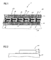
- FIG. 1 shows a device for detecting thermal radiation in a lateral cross-section.
- FIG. 2 shows a detector element on a detector carrier in a lateral cross-section.
- the device 1 for detecting thermal radiation has a stack 10 with a membrane 11 with a detector array 110 of thermal detector element 111 for converting the heat radiation into electrical signals, a circuit carrier 12 with a readout circuit 121 for reading the electrical signals, and at least one cover 13 for Covering the detector elements, wherein the membrane and the cover are arranged in such a way that between the detector elements of the detector carrier and the cover is a, limited by the detector carrier and the cover, cover-side cavity 14 of the stack, the circuit carrier and are arranged together that between the detector carrier and the circuit carrier at least one, the circuit carrier and the detector carrier limited, circuit-side cavity 15 of the stack is present and the cavities are evacuated.
- the cavities communicate with each other through slots through the membrane.
- the detector elements are pyroelectric detector elements in thin-film construction with two electrode layers 112 and a pyroelectric layer 113 arranged between the electrode layers (FIG. 3).
- the pyroelectric layer is an approximately 1 micron thick layer of PZT as a pyroelectric sensitive material.
- the electrode layers are made of platinum and a chromium-nickel alloy with layer thicknesses of about 20 nm.
- the membrane is a Si 3 N 4 / SiO 2 / Si 3 N 4 triple layer.
- a readout circuit is integrated in the circuit carrier.
- the circuit carrier and the cover are each silicon substrates.
- the detector elements are disposed within the first stack cavity opposite a cover recess, not shown, of the cover. In the region of the recess, a common irradiation window 17 is arranged, through which the heat radiation reaches detector elements. The irradiation takes place from the front.
- the material connection consists of a solder.
- the supports (silicon substrates) are soldered together.
- the material bond is made by bonding.
- the procedure is as follows: providing a sacrificial carrier made of silicon, arranging a membrane with plated-through holes on a surface portion of the sacrificial carrier and removing sacrificial material, so that the membrane is at least partially exposed. To remove the silicon, a backside etching away of silicon up to the membrane is carried out. What remains is the membrane with the via, which is then connected to the circuit board.
- the production of the via can be done in any process steps.
- the following further method steps are carried out before arranging the membrane on the sacrificial carrier or after arranging the membrane on the sacrificial carrier: f) generating a bore in the membrane and g) filling the bore with electrically conductive material, so that the electrical Through connection arises.
- the stack cavities are evacuated as they form. Alternatively, the stack cavities are evacuated after making the fabric shutters.
- the stack is provided with a wrapper 20.
- a wrapper 20 For this purpose, an uncrosslinked plastic is applied to the stack in an injection molding process and then crosslinked. Alternatively, a molding process is performed. It is ensured that the irradiation window of the cover remains free, so it is not covered.
- the membrane with the Detector array, the circuit carrier with the read-out circuit and the cover provided and firmly interconnected as described above.
- the manufacturing takes place at the wafer level.
- silicon wafers are provided with a multiplicity of corresponding functionalities (readout circuits, possibly cover recesses).
- the circuit carrier with the membrane and the cover are provided. These functionalized silicon wafers are firmly bonded together as described above.
- a wafer stack is made with a plurality of single stacks. After joining, the individual stacks are separated by sawing the wafer stack and each provided with a cladding.
- the device is used in a motion detector or presence detector.
- a plurality of stacks or devices, each with a stack is present.
Landscapes
- Physics & Mathematics (AREA)
- General Physics & Mathematics (AREA)
- Spectroscopy & Molecular Physics (AREA)
- Engineering & Computer Science (AREA)
- Power Engineering (AREA)
- Chemical & Material Sciences (AREA)
- Nanotechnology (AREA)
- Photometry And Measurement Of Optical Pulse Characteristics (AREA)
- Radiation Pyrometers (AREA)
- Micromachines (AREA)
Applications Claiming Priority (2)
| Application Number | Priority Date | Filing Date | Title |
|---|---|---|---|
| DE200710024902 DE102007024902B8 (de) | 2007-05-29 | 2007-05-29 | Vorrichtung mit Membranstruktur zur Detektion von Wärmestrahlung, Verfahren zum Herstellen und Verwendung der Vorrichtung |
| PCT/EP2008/004246 WO2008145353A1 (de) | 2007-05-29 | 2008-05-28 | Vorrichtung mit membranstruktur zur detektion von wärmestrahlung, verfahren zum herstellen und verwendung der vorrichtung |
Publications (2)
| Publication Number | Publication Date |
|---|---|
| EP2153187A1 EP2153187A1 (de) | 2010-02-17 |
| EP2153187B1 true EP2153187B1 (de) | 2013-01-16 |
Family
ID=39708794
Family Applications (1)
| Application Number | Title | Priority Date | Filing Date |
|---|---|---|---|
| EP20080758829 Not-in-force EP2153187B1 (de) | 2007-05-29 | 2008-05-28 | Vorrichtung mit membranstruktur zur detektion von wärmestrahlung, verfahren zum herstellen und verwendung der vorrichtung |
Country Status (10)
| Country | Link |
|---|---|
| US (1) | US9279730B2 (enExample) |
| EP (1) | EP2153187B1 (enExample) |
| JP (1) | JP2010528300A (enExample) |
| KR (1) | KR101612400B1 (enExample) |
| CN (1) | CN101688810B (enExample) |
| AU (1) | AU2008256413B2 (enExample) |
| BR (1) | BRPI0812099B1 (enExample) |
| DE (1) | DE102007024902B8 (enExample) |
| RU (1) | RU2468346C2 (enExample) |
| WO (1) | WO2008145353A1 (enExample) |
Families Citing this family (8)
| Publication number | Priority date | Publication date | Assignee | Title |
|---|---|---|---|---|
| DE102009017845B4 (de) * | 2009-04-17 | 2011-07-21 | Pyreos Ltd. | Infrarotlichtsensor mit hoher Signalspannung und hohem Signal-Rausch-Verhältnis, sowie Infrarotlichtdetektor mit dem Infrarotlichtsensor |
| DE102009060217B3 (de) | 2009-12-23 | 2011-06-22 | Pyreos Ltd. | Verfahren zum Herstellen eines Infrarotlichtdetektors |
| DE102010012701B4 (de) | 2010-03-24 | 2013-10-17 | Bundesrepublik Deutschland, vertr.d.d. Bundesministerium für Wirtschaft und Technologie, d.vertr.d.d. Präsidenten der Physikalisch-Technischen Bundesanstalt | Mikrokraftsensor |
| DE102012216618A1 (de) | 2012-09-18 | 2014-03-20 | Robert Bosch Gmbh | Anordnung von mindestens zwei Wafern zum Detektieren von elektromagnetischer Strahlung und Verfahren zum Herstellen der Anordnung |
| DE102012217881A1 (de) * | 2012-10-01 | 2014-04-03 | Siemens Aktiengesellschaft | Sensoranordnung und Herstellungsverfahren |
| DE102013204763A1 (de) * | 2013-03-19 | 2014-09-25 | Robert Bosch Gmbh | Mikromechanische Sensorvorrichtung und entsprechendes Herstellungsverfahren |
| US10323979B2 (en) * | 2015-06-01 | 2019-06-18 | Seoul Viosys Co., Ltd. | Ultraviolet measuring device, photodetector element, ultraviolet detector, ultraviolet index calculation device, and electronic device including same |
| CN108827676B (zh) * | 2018-04-25 | 2020-12-11 | 合肥美的电冰箱有限公司 | 散热测量系统及其方法、控制装置 |
Family Cites Families (30)
| Publication number | Priority date | Publication date | Assignee | Title |
|---|---|---|---|---|
| US4044251A (en) * | 1976-05-18 | 1977-08-23 | Minnesota Mining And Manufacturing Company | Electromagnetic radiation detector with large area sensing medium |
| JPH01308927A (ja) | 1988-06-07 | 1989-12-13 | Matsushita Electric Ind Co Ltd | 焦電形赤外検出素子アレイ、焦電形赤外検出器およびその製法 |
| GB9009117D0 (en) | 1990-04-24 | 1990-08-08 | Emi Plc Thorn | Pyroelectric detector and method of manufacturing the same |
| JP3200657B2 (ja) * | 1992-04-30 | 2001-08-20 | テルモ株式会社 | 赤外線センサ |
| JPH07128140A (ja) | 1993-10-29 | 1995-05-19 | Matsushita Electric Works Ltd | 赤外線検出素子 |
| CA2179052C (en) | 1993-12-13 | 2001-02-13 | Robert E. Higashi | Integrated silicon vacuum micropackage for infrared devices |
| DE19525071A1 (de) * | 1995-07-10 | 1997-01-16 | Siemens Ag | Pyroelektrisches Bauelement und Verfahren zur Herstellung |
| JP3399399B2 (ja) * | 1999-04-14 | 2003-04-21 | 株式会社村田製作所 | 赤外線センサ及びその製造方法 |
| DE19932308C2 (de) * | 1999-07-10 | 2001-10-25 | Bosch Gmbh Robert | Sensor, insbesondere Thermosensor |
| DE10004216C2 (de) * | 2000-02-01 | 2002-09-19 | Siemens Ag | Vorrichtung zur Detektion von Wärmestrahlung und Verwendung der Vorrichtung |
| JP2001326367A (ja) * | 2000-05-12 | 2001-11-22 | Denso Corp | センサおよびその製造方法 |
| DE10042945A1 (de) * | 2000-08-31 | 2002-03-28 | Siemens Ag | Bauelement für Sensoren mit integrierter Elektronik und Verfahren zu seiner Herstellung, sowie Sensor mit integrierter Elektronik |
| DE10058861A1 (de) | 2000-11-27 | 2002-06-13 | Siemens Ag | Infrarotsensor für hochauflösende Infrarot-Detektoranordnungen und Verfahren zu seiner Herstellung |
| JP3519720B2 (ja) * | 2001-06-11 | 2004-04-19 | 松下電器産業株式会社 | 電子デバイス |
| JP3604130B2 (ja) | 2001-12-04 | 2004-12-22 | 株式会社アイ・エイチ・アイ・エアロスペース | 熱型赤外線検出素子およびその製造方法ならびに熱型赤外線検出素子アレイ |
| JP2004093535A (ja) | 2002-09-04 | 2004-03-25 | Mitsubishi Electric Corp | 熱型赤外線固体撮像装置およびその製造方法 |
| US6902759B2 (en) * | 2002-09-12 | 2005-06-07 | Innovaquartz Incorporated | Technique for coating or marking glass strands |
| FR2844635B1 (fr) * | 2002-09-16 | 2005-08-19 | Commissariat Energie Atomique | Dispositif detecteur de rayonnement electromagnetique avec boitier integre comportant deux detecteurs superposes |
| JP2004239708A (ja) * | 2003-02-05 | 2004-08-26 | Mitsubishi Electric Corp | 赤外線検出装置およびその製造方法 |
| KR100538996B1 (ko) * | 2003-06-19 | 2005-12-27 | 한국전자통신연구원 | 적외선 흡수층으로 실리콘 산화막을 사용한 적외선 센서및 그 제조 방법 |
| DE10327694A1 (de) * | 2003-06-20 | 2005-01-05 | Robert Bosch Gmbh | Optische Sensoranordnung und entsprechendes Herstellungsverfahren |
| RU2258207C1 (ru) * | 2004-01-09 | 2005-08-10 | Федеральное государственное унитарное предприятие "Научно-производственное предприятие "Исток" | Болометрический резистивный элемент |
| JP2005241457A (ja) * | 2004-02-26 | 2005-09-08 | Hamamatsu Photonics Kk | 赤外線センサ及びその製造方法 |
| FR2867273B1 (fr) * | 2004-03-04 | 2006-09-08 | Commissariat Energie Atomique | Procede de realisation d'un dispositif pour la detection thermique d'un rayonnement comportant un microbolometre actif et un microbolometre passif |
| JP4385255B2 (ja) * | 2004-06-10 | 2009-12-16 | 日本電気株式会社 | ボロメータ型赤外線検出器及び残像の低減方法 |
| JP2005043381A (ja) * | 2004-10-18 | 2005-02-17 | Nec Corp | 熱型赤外線検出器およびその製造方法 |
| US7718967B2 (en) * | 2005-01-26 | 2010-05-18 | Analog Devices, Inc. | Die temperature sensors |
| FR2883417B1 (fr) * | 2005-03-16 | 2007-05-11 | Ulis Soc Par Actions Simplifie | Detecteur bolometrique, dispositif de detection infrarouge mettant en oeuvre un tel detecteur et procede de fabrication de ce detecteur |
| JP2008544263A (ja) * | 2005-06-27 | 2008-12-04 | エイチエル−プラナー・テクニク・ゲゼルシヤフト・ミツト・ベシユレンクテル・ハフツング | 電磁波検出用装置及びそのような装置製造のための方法 |
| WO2007054111A1 (de) * | 2005-11-10 | 2007-05-18 | Fraunhofer-Gesellschaft zur Förderung der angewandten Forschung e.V. | Sensor zum erfassen einer elektromagnetischen strahlung |
-
2007
- 2007-05-29 DE DE200710024902 patent/DE102007024902B8/de not_active Expired - Fee Related
-
2008
- 2008-05-28 KR KR1020097027210A patent/KR101612400B1/ko not_active Expired - Fee Related
- 2008-05-28 AU AU2008256413A patent/AU2008256413B2/en not_active Ceased
- 2008-05-28 US US12/601,556 patent/US9279730B2/en not_active Expired - Fee Related
- 2008-05-28 EP EP20080758829 patent/EP2153187B1/de not_active Not-in-force
- 2008-05-28 BR BRPI0812099-4A patent/BRPI0812099B1/pt not_active IP Right Cessation
- 2008-05-28 JP JP2010509728A patent/JP2010528300A/ja active Pending
- 2008-05-28 WO PCT/EP2008/004246 patent/WO2008145353A1/de not_active Ceased
- 2008-05-28 CN CN2008800235048A patent/CN101688810B/zh not_active Expired - Fee Related
- 2008-05-28 RU RU2009144001/28A patent/RU2468346C2/ru not_active IP Right Cessation
Also Published As
| Publication number | Publication date |
|---|---|
| JP2010528300A (ja) | 2010-08-19 |
| CN101688810B (zh) | 2013-09-18 |
| CN101688810A (zh) | 2010-03-31 |
| DE102007024902A1 (de) | 2008-12-11 |
| AU2008256413B2 (en) | 2013-09-12 |
| BRPI0812099A2 (pt) | 2014-11-25 |
| US20110006211A1 (en) | 2011-01-13 |
| EP2153187A1 (de) | 2010-02-17 |
| WO2008145353A1 (de) | 2008-12-04 |
| KR101612400B1 (ko) | 2016-04-14 |
| KR20100023007A (ko) | 2010-03-03 |
| RU2009144001A (ru) | 2011-07-10 |
| DE102007024902B8 (de) | 2010-12-30 |
| AU2008256413A1 (en) | 2008-12-04 |
| DE102007024902B4 (de) | 2010-08-26 |
| US9279730B2 (en) | 2016-03-08 |
| BRPI0812099B1 (pt) | 2018-06-19 |
| RU2468346C2 (ru) | 2012-11-27 |
Similar Documents
| Publication | Publication Date | Title |
|---|---|---|
| EP2153187B1 (de) | Vorrichtung mit membranstruktur zur detektion von wärmestrahlung, verfahren zum herstellen und verwendung der vorrichtung | |
| DE102013108353B4 (de) | Vorrichtung mit einer eingebetteten MEMS-Vorrichtung und Verfahren zur Herstellung einer eingebetteten MEMS-Vorrichtung | |
| EP2153188B1 (de) | Vorrichtung mit sandwichstruktur zur detektion von wärmestrahlung, verfahren zum herstellen und verwendung der vorrichtung | |
| WO2006122529A2 (de) | Thermopile infrarot sensorarray | |
| DE102013208814A1 (de) | Integrierter Drehraten- und Beschleunigungssensor und Verfahren zur Herstellung eines integrierten Drehraten- und Beschleunigungssensor | |
| DE102007001518B4 (de) | Vorrichtung und Verfahren zum Häusen eines mikromechanischen oder mikrooptoelektronischen Systems | |
| DE112013007109B4 (de) | Gehäuse für mikroelektromechanische Systemvorrichtungen und Verfahren zur Herstellung des Gehäuses für mikroelektromechanische Systemvorrichtungen | |
| EP2223343B1 (de) | Vorrichtung mit einer abgeschirmten sandwichstruktur zur detektion von wärmestrahlung und verwendung der vorrichtung | |
| EP3997428B1 (de) | Verfahren zum herstellen eines hochauflösenden thermischen infrarot-sensor arrays in einem vakuumgefüllten waferlevel gehäuse | |
| DE102007046451B4 (de) | Vorrichtung zur Detektion von Wärmestrahlung mit hoher Auflösung, Verfahren zum Herstellen und Verwendung der Vorrichtung | |
| DE102012224432A1 (de) | Elektrische Schaltung und Verfahren zum Herstellen einer elektrischen Schaltung | |
| DE10004216C2 (de) | Vorrichtung zur Detektion von Wärmestrahlung und Verwendung der Vorrichtung | |
| DE10058861A1 (de) | Infrarotsensor für hochauflösende Infrarot-Detektoranordnungen und Verfahren zu seiner Herstellung | |
| DE4105591C1 (en) | IR sensor in the form of pyroelectric detector - has silicon@ substrate with pyroelectric sensor film metallise to a pattern | |
| DE102014204035A1 (de) | Hybrid integriertes Bauteil und Verfahren zu dessen Herstellung | |
| DE102015213999A1 (de) | Herstellungsverfahren für eine mikroelektronische Bauelementanordnung und mikroelektronische Bauelementanordnung |
Legal Events
| Date | Code | Title | Description |
|---|---|---|---|
| PUAI | Public reference made under article 153(3) epc to a published international application that has entered the european phase |
Free format text: ORIGINAL CODE: 0009012 |
|
| 17P | Request for examination filed |
Effective date: 20091222 |
|
| AK | Designated contracting states |
Kind code of ref document: A1 Designated state(s): AT BE BG CH CY CZ DE DK EE ES FI FR GB GR HR HU IE IS IT LI LT LU LV MC MT NL NO PL PT RO SE SI SK TR |
|
| AX | Request for extension of the european patent |
Extension state: AL BA MK RS |
|
| DAX | Request for extension of the european patent (deleted) | ||
| 17Q | First examination report despatched |
Effective date: 20100907 |
|
| REG | Reference to a national code |
Ref country code: DE Ref legal event code: R079 Ref document number: 502008009133 Country of ref document: DE Free format text: PREVIOUS MAIN CLASS: G01J0005040000 Ipc: G01J0005340000 |
|
| RIC1 | Information provided on ipc code assigned before grant |
Ipc: G01J 5/34 20060101AFI20120727BHEP Ipc: G01J 5/04 20060101ALI20120727BHEP |
|
| GRAP | Despatch of communication of intention to grant a patent |
Free format text: ORIGINAL CODE: EPIDOSNIGR1 |
|
| GRAS | Grant fee paid |
Free format text: ORIGINAL CODE: EPIDOSNIGR3 |
|
| GRAA | (expected) grant |
Free format text: ORIGINAL CODE: 0009210 |
|
| AK | Designated contracting states |
Kind code of ref document: B1 Designated state(s): AT BE BG CH CY CZ DE DK EE ES FI FR GB GR HR HU IE IS IT LI LT LU LV MC MT NL NO PL PT RO SE SI SK TR |
|
| REG | Reference to a national code |
Ref country code: GB Ref legal event code: FG4D Free format text: NOT ENGLISH |
|
| REG | Reference to a national code |
Ref country code: CH Ref legal event code: EP |
|
| REG | Reference to a national code |
Ref country code: IE Ref legal event code: FG4D Free format text: LANGUAGE OF EP DOCUMENT: GERMAN |
|
| REG | Reference to a national code |
Ref country code: AT Ref legal event code: REF Ref document number: 594118 Country of ref document: AT Kind code of ref document: T Effective date: 20130215 Ref country code: CH Ref legal event code: EP |
|
| REG | Reference to a national code |
Ref country code: DE Ref legal event code: R096 Ref document number: 502008009133 Country of ref document: DE Effective date: 20130314 |
|
| REG | Reference to a national code |
Ref country code: NL Ref legal event code: VDEP Effective date: 20130116 |
|
| REG | Reference to a national code |
Ref country code: LT Ref legal event code: MG4D |
|
| PG25 | Lapsed in a contracting state [announced via postgrant information from national office to epo] |
Ref country code: NO Free format text: LAPSE BECAUSE OF FAILURE TO SUBMIT A TRANSLATION OF THE DESCRIPTION OR TO PAY THE FEE WITHIN THE PRESCRIBED TIME-LIMIT Effective date: 20130416 Ref country code: SE Free format text: LAPSE BECAUSE OF FAILURE TO SUBMIT A TRANSLATION OF THE DESCRIPTION OR TO PAY THE FEE WITHIN THE PRESCRIBED TIME-LIMIT Effective date: 20130116 Ref country code: LT Free format text: LAPSE BECAUSE OF FAILURE TO SUBMIT A TRANSLATION OF THE DESCRIPTION OR TO PAY THE FEE WITHIN THE PRESCRIBED TIME-LIMIT Effective date: 20130116 Ref country code: ES Free format text: LAPSE BECAUSE OF FAILURE TO SUBMIT A TRANSLATION OF THE DESCRIPTION OR TO PAY THE FEE WITHIN THE PRESCRIBED TIME-LIMIT Effective date: 20130427 Ref country code: BG Free format text: LAPSE BECAUSE OF FAILURE TO SUBMIT A TRANSLATION OF THE DESCRIPTION OR TO PAY THE FEE WITHIN THE PRESCRIBED TIME-LIMIT Effective date: 20130416 Ref country code: IS Free format text: LAPSE BECAUSE OF FAILURE TO SUBMIT A TRANSLATION OF THE DESCRIPTION OR TO PAY THE FEE WITHIN THE PRESCRIBED TIME-LIMIT Effective date: 20130516 |
|
| PG25 | Lapsed in a contracting state [announced via postgrant information from national office to epo] |
Ref country code: PT Free format text: LAPSE BECAUSE OF FAILURE TO SUBMIT A TRANSLATION OF THE DESCRIPTION OR TO PAY THE FEE WITHIN THE PRESCRIBED TIME-LIMIT Effective date: 20130516 Ref country code: NL Free format text: LAPSE BECAUSE OF FAILURE TO SUBMIT A TRANSLATION OF THE DESCRIPTION OR TO PAY THE FEE WITHIN THE PRESCRIBED TIME-LIMIT Effective date: 20130116 Ref country code: LV Free format text: LAPSE BECAUSE OF FAILURE TO SUBMIT A TRANSLATION OF THE DESCRIPTION OR TO PAY THE FEE WITHIN THE PRESCRIBED TIME-LIMIT Effective date: 20130116 Ref country code: FI Free format text: LAPSE BECAUSE OF FAILURE TO SUBMIT A TRANSLATION OF THE DESCRIPTION OR TO PAY THE FEE WITHIN THE PRESCRIBED TIME-LIMIT Effective date: 20130116 Ref country code: GR Free format text: LAPSE BECAUSE OF FAILURE TO SUBMIT A TRANSLATION OF THE DESCRIPTION OR TO PAY THE FEE WITHIN THE PRESCRIBED TIME-LIMIT Effective date: 20130417 Ref country code: PL Free format text: LAPSE BECAUSE OF FAILURE TO SUBMIT A TRANSLATION OF THE DESCRIPTION OR TO PAY THE FEE WITHIN THE PRESCRIBED TIME-LIMIT Effective date: 20130116 Ref country code: SI Free format text: LAPSE BECAUSE OF FAILURE TO SUBMIT A TRANSLATION OF THE DESCRIPTION OR TO PAY THE FEE WITHIN THE PRESCRIBED TIME-LIMIT Effective date: 20130116 |
|
| PG25 | Lapsed in a contracting state [announced via postgrant information from national office to epo] |
Ref country code: HR Free format text: LAPSE BECAUSE OF FAILURE TO SUBMIT A TRANSLATION OF THE DESCRIPTION OR TO PAY THE FEE WITHIN THE PRESCRIBED TIME-LIMIT Effective date: 20130116 |
|
| PG25 | Lapsed in a contracting state [announced via postgrant information from national office to epo] |
Ref country code: CZ Free format text: LAPSE BECAUSE OF FAILURE TO SUBMIT A TRANSLATION OF THE DESCRIPTION OR TO PAY THE FEE WITHIN THE PRESCRIBED TIME-LIMIT Effective date: 20130116 Ref country code: RO Free format text: LAPSE BECAUSE OF FAILURE TO SUBMIT A TRANSLATION OF THE DESCRIPTION OR TO PAY THE FEE WITHIN THE PRESCRIBED TIME-LIMIT Effective date: 20130116 Ref country code: DK Free format text: LAPSE BECAUSE OF FAILURE TO SUBMIT A TRANSLATION OF THE DESCRIPTION OR TO PAY THE FEE WITHIN THE PRESCRIBED TIME-LIMIT Effective date: 20130116 Ref country code: SK Free format text: LAPSE BECAUSE OF FAILURE TO SUBMIT A TRANSLATION OF THE DESCRIPTION OR TO PAY THE FEE WITHIN THE PRESCRIBED TIME-LIMIT Effective date: 20130116 Ref country code: EE Free format text: LAPSE BECAUSE OF FAILURE TO SUBMIT A TRANSLATION OF THE DESCRIPTION OR TO PAY THE FEE WITHIN THE PRESCRIBED TIME-LIMIT Effective date: 20130116 |
|
| PLBE | No opposition filed within time limit |
Free format text: ORIGINAL CODE: 0009261 |
|
| STAA | Information on the status of an ep patent application or granted ep patent |
Free format text: STATUS: NO OPPOSITION FILED WITHIN TIME LIMIT |
|
| PG25 | Lapsed in a contracting state [announced via postgrant information from national office to epo] |
Ref country code: CY Free format text: LAPSE BECAUSE OF FAILURE TO SUBMIT A TRANSLATION OF THE DESCRIPTION OR TO PAY THE FEE WITHIN THE PRESCRIBED TIME-LIMIT Effective date: 20130116 |
|
| BERE | Be: lapsed |
Owner name: PYREOS LTD. Effective date: 20130531 |
|
| REG | Reference to a national code |
Ref country code: DE Ref legal event code: R119 Ref document number: 502008009133 Country of ref document: DE |
|
| 26N | No opposition filed |
Effective date: 20131017 |
|
| PG25 | Lapsed in a contracting state [announced via postgrant information from national office to epo] |
Ref country code: IT Free format text: LAPSE BECAUSE OF FAILURE TO SUBMIT A TRANSLATION OF THE DESCRIPTION OR TO PAY THE FEE WITHIN THE PRESCRIBED TIME-LIMIT Effective date: 20130116 Ref country code: MC Free format text: LAPSE BECAUSE OF FAILURE TO SUBMIT A TRANSLATION OF THE DESCRIPTION OR TO PAY THE FEE WITHIN THE PRESCRIBED TIME-LIMIT Effective date: 20130116 |
|
| PG25 | Lapsed in a contracting state [announced via postgrant information from national office to epo] |
Ref country code: DE Free format text: LAPSE BECAUSE OF NON-PAYMENT OF DUE FEES Effective date: 20131203 |
|
| REG | Reference to a national code |
Ref country code: DE Ref legal event code: R097 Ref document number: 502008009133 Country of ref document: DE Effective date: 20131017 |
|
| REG | Reference to a national code |
Ref country code: IE Ref legal event code: MM4A |
|
| PG25 | Lapsed in a contracting state [announced via postgrant information from national office to epo] |
Ref country code: BE Free format text: LAPSE BECAUSE OF NON-PAYMENT OF DUE FEES Effective date: 20130531 |
|
| REG | Reference to a national code |
Ref country code: DE Ref legal event code: R119 Ref document number: 502008009133 Country of ref document: DE Effective date: 20131203 |
|
| PG25 | Lapsed in a contracting state [announced via postgrant information from national office to epo] |
Ref country code: IE Free format text: LAPSE BECAUSE OF NON-PAYMENT OF DUE FEES Effective date: 20130528 |
|
| REG | Reference to a national code |
Ref country code: AT Ref legal event code: MM01 Ref document number: 594118 Country of ref document: AT Kind code of ref document: T Effective date: 20130528 |
|
| PG25 | Lapsed in a contracting state [announced via postgrant information from national office to epo] |
Ref country code: AT Free format text: LAPSE BECAUSE OF NON-PAYMENT OF DUE FEES Effective date: 20130528 |
|
| PG25 | Lapsed in a contracting state [announced via postgrant information from national office to epo] |
Ref country code: MT Free format text: LAPSE BECAUSE OF FAILURE TO SUBMIT A TRANSLATION OF THE DESCRIPTION OR TO PAY THE FEE WITHIN THE PRESCRIBED TIME-LIMIT Effective date: 20130116 |
|
| REG | Reference to a national code |
Ref country code: FR Ref legal event code: PLFP Year of fee payment: 8 |
|
| PG25 | Lapsed in a contracting state [announced via postgrant information from national office to epo] |
Ref country code: TR Free format text: LAPSE BECAUSE OF FAILURE TO SUBMIT A TRANSLATION OF THE DESCRIPTION OR TO PAY THE FEE WITHIN THE PRESCRIBED TIME-LIMIT Effective date: 20130116 |
|
| PG25 | Lapsed in a contracting state [announced via postgrant information from national office to epo] |
Ref country code: LU Free format text: LAPSE BECAUSE OF NON-PAYMENT OF DUE FEES Effective date: 20130528 Ref country code: HU Free format text: LAPSE BECAUSE OF FAILURE TO SUBMIT A TRANSLATION OF THE DESCRIPTION OR TO PAY THE FEE WITHIN THE PRESCRIBED TIME-LIMIT; INVALID AB INITIO Effective date: 20080528 |
|
| REG | Reference to a national code |
Ref country code: FR Ref legal event code: PLFP Year of fee payment: 9 |
|
| REG | Reference to a national code |
Ref country code: FR Ref legal event code: PLFP Year of fee payment: 10 |
|
| REG | Reference to a national code |
Ref country code: CH Ref legal event code: PCAR Free format text: NEW ADDRESS: HOLEESTRASSE 87, 4054 BASEL (CH) |
|
| REG | Reference to a national code |
Ref country code: FR Ref legal event code: PLFP Year of fee payment: 11 |
|
| PGFP | Annual fee paid to national office [announced via postgrant information from national office to epo] |
Ref country code: CH Payment date: 20180523 Year of fee payment: 11 |
|
| PGFP | Annual fee paid to national office [announced via postgrant information from national office to epo] |
Ref country code: FR Payment date: 20180523 Year of fee payment: 11 |
|
| PGFP | Annual fee paid to national office [announced via postgrant information from national office to epo] |
Ref country code: GB Payment date: 20180523 Year of fee payment: 11 |
|
| REG | Reference to a national code |
Ref country code: CH Ref legal event code: PL |
|
| GBPC | Gb: european patent ceased through non-payment of renewal fee |
Effective date: 20190528 |
|
| PG25 | Lapsed in a contracting state [announced via postgrant information from national office to epo] |
Ref country code: CH Free format text: LAPSE BECAUSE OF NON-PAYMENT OF DUE FEES Effective date: 20190531 Ref country code: LI Free format text: LAPSE BECAUSE OF NON-PAYMENT OF DUE FEES Effective date: 20190531 |
|
| PG25 | Lapsed in a contracting state [announced via postgrant information from national office to epo] |
Ref country code: GB Free format text: LAPSE BECAUSE OF NON-PAYMENT OF DUE FEES Effective date: 20190528 |
|
| PG25 | Lapsed in a contracting state [announced via postgrant information from national office to epo] |
Ref country code: FR Free format text: LAPSE BECAUSE OF NON-PAYMENT OF DUE FEES Effective date: 20190531 |