EP2148317B1 - Halbleiteranordnung zum Treiben eines Geräts mit einem Stromverbraucher und Gerät mit einem Stromverbraucher mit dieser Halbleiteranordnung - Google Patents
Halbleiteranordnung zum Treiben eines Geräts mit einem Stromverbraucher und Gerät mit einem Stromverbraucher mit dieser Halbleiteranordnung Download PDFInfo
- Publication number
- EP2148317B1 EP2148317B1 EP09173037.4A EP09173037A EP2148317B1 EP 2148317 B1 EP2148317 B1 EP 2148317B1 EP 09173037 A EP09173037 A EP 09173037A EP 2148317 B1 EP2148317 B1 EP 2148317B1
- Authority
- EP
- European Patent Office
- Prior art keywords
- current
- transistor
- output
- tft
- signal
- Prior art date
- Legal status (The legal status is an assumption and is not a legal conclusion. Google has not performed a legal analysis and makes no representation as to the accuracy of the status listed.)
- Expired - Lifetime
Links
- 239000004065 semiconductor Substances 0.000 title claims description 50
- 238000006243 chemical reaction Methods 0.000 claims description 222
- 238000010586 diagram Methods 0.000 description 56
- 239000011159 matrix material Substances 0.000 description 24
- 229920006395 saturated elastomer Polymers 0.000 description 11
- 239000003086 colorant Substances 0.000 description 10
- 230000000694 effects Effects 0.000 description 10
- 101150016164 msw1 gene Proteins 0.000 description 10
- 239000000872 buffer Substances 0.000 description 9
- 238000007599 discharging Methods 0.000 description 9
- 230000001276 controlling effect Effects 0.000 description 5
- 238000000034 method Methods 0.000 description 4
- 239000010409 thin film Substances 0.000 description 3
- 230000004048 modification Effects 0.000 description 2
- 238000012986 modification Methods 0.000 description 2
- 230000001105 regulatory effect Effects 0.000 description 2
- 239000000758 substrate Substances 0.000 description 2
- 101100489584 Solanum lycopersicum TFT1 gene Proteins 0.000 description 1
- 230000003247 decreasing effect Effects 0.000 description 1
- 230000001419 dependent effect Effects 0.000 description 1
- 238000005401 electroluminescence Methods 0.000 description 1
- 239000011521 glass Substances 0.000 description 1
- 239000004973 liquid crystal related substance Substances 0.000 description 1
- 230000003071 parasitic effect Effects 0.000 description 1
- 229910021420 polycrystalline silicon Inorganic materials 0.000 description 1
- 230000000630 rising effect Effects 0.000 description 1
- 230000001360 synchronised effect Effects 0.000 description 1
Images


Classifications
-
- G—PHYSICS
- G09—EDUCATION; CRYPTOGRAPHY; DISPLAY; ADVERTISING; SEALS
- G09G—ARRANGEMENTS OR CIRCUITS FOR CONTROL OF INDICATING DEVICES USING STATIC MEANS TO PRESENT VARIABLE INFORMATION
- G09G3/00—Control arrangements or circuits, of interest only in connection with visual indicators other than cathode-ray tubes
- G09G3/20—Control arrangements or circuits, of interest only in connection with visual indicators other than cathode-ray tubes for presentation of an assembly of a number of characters, e.g. a page, by composing the assembly by combination of individual elements arranged in a matrix no fixed position being assigned to or needed to be assigned to the individual characters or partial characters
- G09G3/22—Control arrangements or circuits, of interest only in connection with visual indicators other than cathode-ray tubes for presentation of an assembly of a number of characters, e.g. a page, by composing the assembly by combination of individual elements arranged in a matrix no fixed position being assigned to or needed to be assigned to the individual characters or partial characters using controlled light sources
- G09G3/30—Control arrangements or circuits, of interest only in connection with visual indicators other than cathode-ray tubes for presentation of an assembly of a number of characters, e.g. a page, by composing the assembly by combination of individual elements arranged in a matrix no fixed position being assigned to or needed to be assigned to the individual characters or partial characters using controlled light sources using electroluminescent panels
- G09G3/32—Control arrangements or circuits, of interest only in connection with visual indicators other than cathode-ray tubes for presentation of an assembly of a number of characters, e.g. a page, by composing the assembly by combination of individual elements arranged in a matrix no fixed position being assigned to or needed to be assigned to the individual characters or partial characters using controlled light sources using electroluminescent panels semiconductive, e.g. using light-emitting diodes [LED]
- G09G3/3208—Control arrangements or circuits, of interest only in connection with visual indicators other than cathode-ray tubes for presentation of an assembly of a number of characters, e.g. a page, by composing the assembly by combination of individual elements arranged in a matrix no fixed position being assigned to or needed to be assigned to the individual characters or partial characters using controlled light sources using electroluminescent panels semiconductive, e.g. using light-emitting diodes [LED] organic, e.g. using organic light-emitting diodes [OLED]
- G09G3/3275—Details of drivers for data electrodes
- G09G3/3283—Details of drivers for data electrodes in which the data driver supplies a variable data current for setting the current through, or the voltage across, the light-emitting elements
-
- G—PHYSICS
- G09—EDUCATION; CRYPTOGRAPHY; DISPLAY; ADVERTISING; SEALS
- G09G—ARRANGEMENTS OR CIRCUITS FOR CONTROL OF INDICATING DEVICES USING STATIC MEANS TO PRESENT VARIABLE INFORMATION
- G09G2300/00—Aspects of the constitution of display devices
- G09G2300/08—Active matrix structure, i.e. with use of active elements, inclusive of non-linear two terminal elements, in the pixels together with light emitting or modulating elements
- G09G2300/0809—Several active elements per pixel in active matrix panels
- G09G2300/0842—Several active elements per pixel in active matrix panels forming a memory circuit, e.g. a dynamic memory with one capacitor
-
- G—PHYSICS
- G09—EDUCATION; CRYPTOGRAPHY; DISPLAY; ADVERTISING; SEALS
- G09G—ARRANGEMENTS OR CIRCUITS FOR CONTROL OF INDICATING DEVICES USING STATIC MEANS TO PRESENT VARIABLE INFORMATION
- G09G2310/00—Command of the display device
- G09G2310/02—Addressing, scanning or driving the display screen or processing steps related thereto
- G09G2310/0243—Details of the generation of driving signals
- G09G2310/0248—Precharge or discharge of column electrodes before or after applying exact column voltages
-
- G—PHYSICS
- G09—EDUCATION; CRYPTOGRAPHY; DISPLAY; ADVERTISING; SEALS
- G09G—ARRANGEMENTS OR CIRCUITS FOR CONTROL OF INDICATING DEVICES USING STATIC MEANS TO PRESENT VARIABLE INFORMATION
- G09G2310/00—Command of the display device
- G09G2310/02—Addressing, scanning or driving the display screen or processing steps related thereto
- G09G2310/0264—Details of driving circuits
- G09G2310/027—Details of drivers for data electrodes, the drivers handling digital grey scale data, e.g. use of D/A converters
-
- G—PHYSICS
- G09—EDUCATION; CRYPTOGRAPHY; DISPLAY; ADVERTISING; SEALS
- G09G—ARRANGEMENTS OR CIRCUITS FOR CONTROL OF INDICATING DEVICES USING STATIC MEANS TO PRESENT VARIABLE INFORMATION
- G09G2310/00—Command of the display device
- G09G2310/02—Addressing, scanning or driving the display screen or processing steps related thereto
- G09G2310/0264—Details of driving circuits
- G09G2310/0297—Special arrangements with multiplexing or demultiplexing of display data in the drivers for data electrodes, in a pre-processing circuitry delivering display data to said drivers or in the matrix panel, e.g. multiplexing plural data signals to one D/A converter or demultiplexing the D/A converter output to multiple columns
-
- G—PHYSICS
- G09—EDUCATION; CRYPTOGRAPHY; DISPLAY; ADVERTISING; SEALS
- G09G—ARRANGEMENTS OR CIRCUITS FOR CONTROL OF INDICATING DEVICES USING STATIC MEANS TO PRESENT VARIABLE INFORMATION
- G09G2320/00—Control of display operating conditions
- G09G2320/02—Improving the quality of display appearance
- G09G2320/0233—Improving the luminance or brightness uniformity across the screen
-
- G—PHYSICS
- G09—EDUCATION; CRYPTOGRAPHY; DISPLAY; ADVERTISING; SEALS
- G09G—ARRANGEMENTS OR CIRCUITS FOR CONTROL OF INDICATING DEVICES USING STATIC MEANS TO PRESENT VARIABLE INFORMATION
- G09G3/00—Control arrangements or circuits, of interest only in connection with visual indicators other than cathode-ray tubes
- G09G3/20—Control arrangements or circuits, of interest only in connection with visual indicators other than cathode-ray tubes for presentation of an assembly of a number of characters, e.g. a page, by composing the assembly by combination of individual elements arranged in a matrix no fixed position being assigned to or needed to be assigned to the individual characters or partial characters
- G09G3/22—Control arrangements or circuits, of interest only in connection with visual indicators other than cathode-ray tubes for presentation of an assembly of a number of characters, e.g. a page, by composing the assembly by combination of individual elements arranged in a matrix no fixed position being assigned to or needed to be assigned to the individual characters or partial characters using controlled light sources
- G09G3/30—Control arrangements or circuits, of interest only in connection with visual indicators other than cathode-ray tubes for presentation of an assembly of a number of characters, e.g. a page, by composing the assembly by combination of individual elements arranged in a matrix no fixed position being assigned to or needed to be assigned to the individual characters or partial characters using controlled light sources using electroluminescent panels
- G09G3/32—Control arrangements or circuits, of interest only in connection with visual indicators other than cathode-ray tubes for presentation of an assembly of a number of characters, e.g. a page, by composing the assembly by combination of individual elements arranged in a matrix no fixed position being assigned to or needed to be assigned to the individual characters or partial characters using controlled light sources using electroluminescent panels semiconductive, e.g. using light-emitting diodes [LED]
- G09G3/3208—Control arrangements or circuits, of interest only in connection with visual indicators other than cathode-ray tubes for presentation of an assembly of a number of characters, e.g. a page, by composing the assembly by combination of individual elements arranged in a matrix no fixed position being assigned to or needed to be assigned to the individual characters or partial characters using controlled light sources using electroluminescent panels semiconductive, e.g. using light-emitting diodes [LED] organic, e.g. using organic light-emitting diodes [OLED]
- G09G3/3225—Control arrangements or circuits, of interest only in connection with visual indicators other than cathode-ray tubes for presentation of an assembly of a number of characters, e.g. a page, by composing the assembly by combination of individual elements arranged in a matrix no fixed position being assigned to or needed to be assigned to the individual characters or partial characters using controlled light sources using electroluminescent panels semiconductive, e.g. using light-emitting diodes [LED] organic, e.g. using organic light-emitting diodes [OLED] using an active matrix
- G09G3/3233—Control arrangements or circuits, of interest only in connection with visual indicators other than cathode-ray tubes for presentation of an assembly of a number of characters, e.g. a page, by composing the assembly by combination of individual elements arranged in a matrix no fixed position being assigned to or needed to be assigned to the individual characters or partial characters using controlled light sources using electroluminescent panels semiconductive, e.g. using light-emitting diodes [LED] organic, e.g. using organic light-emitting diodes [OLED] using an active matrix with pixel circuitry controlling the current through the light-emitting element
- G09G3/3241—Control arrangements or circuits, of interest only in connection with visual indicators other than cathode-ray tubes for presentation of an assembly of a number of characters, e.g. a page, by composing the assembly by combination of individual elements arranged in a matrix no fixed position being assigned to or needed to be assigned to the individual characters or partial characters using controlled light sources using electroluminescent panels semiconductive, e.g. using light-emitting diodes [LED] organic, e.g. using organic light-emitting diodes [OLED] using an active matrix with pixel circuitry controlling the current through the light-emitting element the current through the light-emitting element being set using a data current provided by the data driver, e.g. by using a two-transistor current mirror
- G09G3/325—Control arrangements or circuits, of interest only in connection with visual indicators other than cathode-ray tubes for presentation of an assembly of a number of characters, e.g. a page, by composing the assembly by combination of individual elements arranged in a matrix no fixed position being assigned to or needed to be assigned to the individual characters or partial characters using controlled light sources using electroluminescent panels semiconductive, e.g. using light-emitting diodes [LED] organic, e.g. using organic light-emitting diodes [OLED] using an active matrix with pixel circuitry controlling the current through the light-emitting element the current through the light-emitting element being set using a data current provided by the data driver, e.g. by using a two-transistor current mirror the data current flowing through the driving transistor during a setting phase, e.g. by using a switch for connecting the driving transistor to the data driver
Definitions
- the present invention relates to a semiconductor device for driving a current load device provided with a plurality of cells including a current load element and a current load device provided therewith, and particularly relates to a semiconductor device for driving a current load device for carrying out a gradation display by a current value to which a current load element is supplied and a current load device provided therewith.
- a current load device provided with a plurality of cells, in the form of a matrix, including a current load element of which operation is decided by current supplied. Its application is, for example, a light emission display device in which a current load element is a luminous element, and an organic EL(Electro Luminescence) display device in which an organic EL element is used as a luminous element.
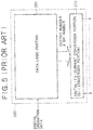
- FIG. 1 shows the constitution of a matrix type light emission display device.
- the display device comprises a horizontal driving circuit 200, a vertical scanning circuit 300 and a display portion 400.
- the gradation display is realized by adjusting current flowing in a luminous element within a 1-pixel display portion 100 of the display portion 400.
- a luminous element whose brightness is decided by various current, current and brightness are in a proportional relation.
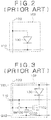
- FIG. 2 is a circuit view showing the constitution of the 1-pixel display portion in case of the simple matrix drive.
- a luminous element 130 is connected between the control line 110 and the signal line 120.
- the control line 110 is driven by the vertical driving circuit 300
- the signal line 120 is driven by the horizontal driving circuit 200.
- control lines 110 are sequentially selected one by one by the vertical scanning circuit 300, and when current or voltage is output to the Lth signal line 120 from the horizontal driving circuit 200 during the scanning of the Kth control line 110, current flowing in the Kth line and the Lth column luminous element is decided, and the luminous element emits with intensity corresponding to the current. Thereafter, when the (K+1)th scanning is started, emitting of the Kth luminous element terminates.
- FIG. 3 is a circuit view showing the constitution of the 1-pixel display portion in case of the active matrix drive.
- a switch SW100 controlled by a potential of the control line 110 is connected to the signal line 110, and a gate of a TFT (Thin Film Transistor) T100 and one end of a capacity element C100 are connected to the other end of the switch SW100.
- a source of the TFT T100 and the other end of the capacity element C100 are grounded, and a luminous element 130 is connected between a drain of the TFT T100 and a signal line whose potential is VEL.
- the switch 100 in the 1-pixel display portion 102 is turned on.
- the Lth output voltage of the horizontal driving circuit 200 is a gate voltage of the TFT T100, and when a gate voltage such that the TFT T100 is operated in a saturated area is applied, impedance of the TFT T100 is decided. As a result, current flowing in the luminous element 130 is decided, and the luminous element 130 emits with intensity corresponding to the current.
- FIGS. 4A and 4B are respectively circuit views showing the other constitution of the 1-pixel display portion in the case of the active matrix drive.
- a switch SW102 controlled by a potential of the control line 110 is connected to the signal line 110, and a gate and a drain of a P channel TFT T302 are connected to the other end of the switch SW102.
- a switch SW101 controlled by a potential of the control line 110 is connected to the gate and the drain, and a gate of the P channel TFT T101 and one end of a capacity element C100 are connected to the other end thereof.
- a constant potential VEL is supplied to sources of the TFT T101 and T102 and the other end of the capacity element C100.
- a luminous element 130 is connected between the drain of the TFT T101 and a ground potential GND.
- the TFT T102 and TFT T101 employ the current mirror constitution, where the current abilities of the TFT T102 and TFT T101 are equal to each other, the same current as the output current value of the horizontal driving circuit 200 flows to the luminous element 130 through the TFT T101, and the luminous element 130 emits with intensity according to the current value.
- the horizontal driving circuit 200 has a function to convert digital gradation data into current or voltage.
- voltage output since unevenness of threshold of a transistor and unevenness of voltage-current characteristics and current-brightness characteristics of the luminous element are present in a pixel circuit (1-pixel display portion), even if the same voltage is applied, there is a high possibility that brightness is uneven.
- current output being influenced merely by the unevenness of the current-brightness characteristics of the luminous element, unevenness of brightness is small, and high brightness can be displayed.
- FIG. 5 is a block diagram showing one example of the constitution of a horizontal scanning circuit 200 for outputting current to a display portion 400.
- digital gradation data are developed to the number of output by a data logic portion 201, and afterwards, the digital gradation data are input into a digital voltage signal to analog current signal (digital-to-current) conversion portion 210 to thereby obtain a current output for the number of output.
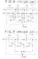
- FIG. 6 is a circuit view showing a first conventional example of a digital-to-current conversion portion for 1-output.
- gradation data are 3 bits (D0 to D2)
- switches SW110, SW111, and SW112 controlled thereby connected in common to an output end for outputting current I data.
- N channels TFT T110, T111, and T112 in which an input voltage VA is supplied to a gate are connected between the switches SW110, Swill, and SW112 and a ground wire at a ground potential VG.
- the current-brightness characteristics of the luminous element are in a proportional relation.
- both the horizontal driving circuit 200 and the vertical driving circuit 300 are formed on a glass substrate, and all transistors are TFT. Even where gradation data are not less than 3 bits, the similar constitution is employed.
- the channel length (L) is constant, and the ratio of the channel width (W) is 1:2:4.
- TFT T110 to T112 are common such that the gate voltage is voltage VA and the source voltage is voltage VG, where TFT T110 to T112 are operated in a saturated area, the current ratio is 1:2:4. So, if a suitable input voltage VA is selected, switches SW110 to SW112 are turned on/off on the basis of gradation data D0 to D2 whereby with respect to the output current I data, current output of 8 gradations whose current ratio is 0 to 7 becomes enabled. Further, the absolute value of current can be regulated by changing the input voltage VA.
- FIG. 7 is a circuit view showing a second conventional example of a digital-to-current conversion portion for 1-output.
- digital gradation data D0 to D2 are input into gates of N channels TFT T110 to T112. Drains of the TFT T110 to T112 are connected in common to output ends and a power supply voltage VD is supplied to sources thereof.
- the ratio of the channel width of the TFT T110 to T112 is set to 1:2:4 similarly to the first conventional example.
- a high level of digital gradation data input is set in advance to a suitable voltage, and a low level is made to be a level turned off by a thin film transistor, whereby current output of 8 gradations whose current ratio is 0 to 7 becomes enabled similarly to the first conventional example. Further, the absolute value of current can be regulated by changing a high level of digital gradation data input.
- the output current value is low, it takes time for driving.
- driving completes at the time when the same current as the output current of the digital-to-current conversion portion as a driving circuit flows to the TFT in the pixel, but a wiring load, particularly a parasitic capacity is always present in the signal line 110 within the display portion 400, the luminous element also has a capacity value, and therefore it is necessary that the capacity loads are charged or discharged by output current which is constant current. That is, since the same current as output current of a digital-to-current conversion circuit which is a driving circuit flows to the TFT within the pixel first by charging or discharging the capacities to a certain voltage, it takes long time till then.
- US-5,552,677 discloses a method and control circuit for precharging a plurality of columns prior to enabling a row of a display.
- a display has pixels organized into columns and rows. The columns are precharged to a reference voltage prior to enabling each of the rows.
- the reference voltage is developed using a reference generator and a buffer.
- US-6,707,438 B1 discloses a driving apparatus for a multi-color light-emitting display panel including drive lines and scanning lines intersecting with each other, and capacitive light-emitting elements which have polarities connected to the scanning lines and the drive lines at the intersections and which are divided into a plurality of types by a color of light emission, the capacitive light-emitting elements of the same type being arranged on each drive line.
- the drive apparatus comprises a scanning circuit for selectively supplying a first potential and a second potential higher than the first potential to each of the scanning lines, and a drive circuit for selectively supplying a drive current from a current source and a third a potential for an offset voltage not higher than a light emission threshold voltage of the element to each of the drive lines, the drive current and the third potential are variable.
- US-6.756.962 B1 discloses a liquid crystal image display comprising differential amplifiers composed of polycrystalline Si TFTs incorporated in buffer for a signal line driver.
- the image display includes buffer outputting switches for turning off the outputs of the buffers and signal line shunting switches for shorting the input and output terminals of the buffer. For the first half of one horizontal period, the signal line shunting switches are held off whereas the buffer outputting switches are held on, to feed signal lines with an image signal voltage selected by level select switches through the buffers.
- the signal line shunting switches are held on whereas the buffer outputting switches are held off, to feed the signal lines directly with the image signal voltage selected by the level select switches, and the signal lines fed with the equal image signal voltages are shorted to prevent the brightness nonuniformity of vertical streaks, as might otherwise be caused because said buffers have different offset voltages.
- WO 99/05667 discloses a cell driving apparatus of a field emission display cabable of increasing a grey level and minimizing an area problem by designing a current mode DAC which contains low voltage devices.
- the cell driving apparatus for use in the field emission display employing a passive matrix indication method wherein the field emission display includes a field emission device cell having a cathode and a gate electrode, and a data driving means outputting digital signals provided from the outside as data signals, comprises a current mode DAC means for providing a current to the cathode in response to the data signals from the data driving means, and a high voltage isolating means, connected between the current mode DAC means and a cathode line, for preventing an instantaneous high voltage from being provided to the current mode DAC means to thereby protect the current mode DAC means, wherein the instantaneous high voltage is generated between a gate line and the cathode line in response to a gate control signal derived from a gate control means.
- the present invention is defined in independent claim 1.
- the dependent claims define embodiments of the invention.
- FIG. 8 is a block diagram showing the constitution of a semiconductor device for a light emission display device according to a first example not part of the present invention.
- a digital-to-current (D/I) conversion portion 210 is provided, and the digital-to-current (D/I) conversion portion 210 is provided with a shift register comprising a 1-output D/I conversion portion 230 for the output number (3 x n) to the light emission display device, and n flip-flops (F/F) 290_1 to 290_n provided every 3-output.
- a start signal IST for controlling timing for storing current
- a clock signal ICL and an inverted signal ICLB of the clock signal ICL.
- any of reference current IR0 to IR2, IG0 to IG2, and IB0 to IB2 for reference are input according to light emitting color assigned thereto.
- reference current has a current value adjusted to the current-brightness characteristics of luminous elements whose light emitting colors are red, blue and green, and a current value ir0 of reference current IR0 corresponds to a first gradation of a luminous element whose emitting color is red, a current value ir1 of reference current IR1 corresponds to a second gradation of a luminous element whose emitting color is red, and a current value ir2 of reference current IR2 corresponds to a fourth gradation of a luminous element whose emitting color is red.
- reference current IG0 to IG2 correspond to a first gradation, a second gradation, and a fourth gradation whose light emitting colors are green, respectively
- reference current IB0 to IB2 correspond to a first gradation, a second gradation, and a fourth gradation whose light emitting colors are blue, respectively.
- One F/F 290 and three 1-output D/I conversion portions 230 into which is input a signal MSW output from the F/F 290 constitute one RGB D/I conversion portion 220.
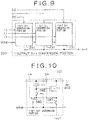
- FIG. 9 is a block diagram showing the constitution of a 1-output D/I conversion portion 230.
- the 1-output D/I conversion portion 230 comprises three 1-bit D/I conversion portions 231. Any of a combination of image data D0 and reference current I0, a combination of image data D1 and reference current I1, and a combination of image data D2 and reference current I2 are input into these 1-bit D/I conversion portions 231. and a signal MSW which is an output signal of F/F is input.
- Reference current I0 to I2 correspond to any of a combination of reference current IR0 to IR2, a combination of reference current IG0 to IG2, and a combination of reference current IB0 to IB2.
- reference current supplied to the 1-bit D/I conversion portion 231 into which is input digital gradation data D0 is reference current IR0 corresponding to brightness of the first gradation of a luminous element for displaying red.
- reference current supplied to the 1-bit D/I conversion portion 231 into which is input digital gradation data D1 is reference current IR1 corresponding to brightness of the second gradation of a luminous element for displaying red
- reference current supplied to the 1-bit D/I conversion portion 231 into which is input digital gradation data D2 is reference current IR2 corresponding to brightness of the fourth gradation of a luminous element for displaying red.
- FIG. 10 is a block diagram showing the constitution of a 1-bit D/I conversion portion 231.
- a current storing and outputting transistor N channel thin film transistor (TFT) T1 switches SW1 to SW3, and a capacity element C1.
- the switch SW1 is connected to a drain of TFT T1, and controlled by gradation data D *.
- Output current lout is output from the other end of the switch SW1.
- the switch SW2 is connected between a contact between the switch SW1 and TFT T1, one end of the capacity element C1 and a gate of TFT T1, and controlled by a signal MSW.
- One end of the switch SW3 is connected to a signal line to which is supplied reference current 1*, and the other end thereof is connected between a contact between the switch SW1 and TFT T1 and one end of the capacity element C1, and controlled by a signal MSW. Further, a source of TFT T1 and the other end of the capacity element C1 are, for example, grounded, but where there is no problem in terms of operation, a voltage higher than a ground voltage GND may be supplied.
- Gradation data D* and reference current I* correspond to any of gradation data D0 and reference current 10, gradation data D1 and reference current I1, and gradation data D1 and reference current I2.
- FIG. 11 is a timing chart showing the operation of a semiconductor device for a light emission display device according to a first embodiment of the present invention.
- Y_1 and Y_2 show respectively a first line and a second line output signals of a vertical scanning circuit 300 (see FIG.
- D0, D1 and D2 show respectively 3-bit digital image data (gradation data)
- lout shows an output signal of the 1-output D/I conversion portion 230
- IST shows a start signal of a shift register constituted by n flip-flops 290
- ICL shows a clock signal of the shift register
- MSW_1 and MSW_2 show respectively a first stage and a second stage output signals of the shift register.
- a period from the beginning of vertical scanning of a display portion 400 (see FIG. 1 ) to the next beginning of vertical scanning is called 1 frame.
- the 1 frame comprises a current driving period (a first operation period) and a current storing period (a second operation period).
- each 1-bit D/I conversion portion 231 stores reference current supplied from a reference current source.
- all digital gradation data are a low level, and the switch SW1 of the 1-bit D/I conversion portion 231 is OFF.
- a pulse signal is input as a start signal IST into F/F 290_1 of the first stage, and simultaneously with the input of the pulse signal, a clock signal ICL and a clock inverted signal ICLB are input into the F/F 290_1, whereby a shift register constituted by n F/F 290s begins to operate.
- an output signal MSW_1 of the F/F 290_1 of the first stage assumes a high level
- the switches SW2 and SW3 of each 1-bit D/I conversion portion 231 provided in the 1-output D/I conversion portion 230 into which is input the output signal MSW_1 are turned ON.
- the current storing and outputting TFT T1 within the 1-bit D/I conversion portion 231 operates in a saturated area because a portion between the gate and the drain is short-circuited. And, in the state that the present operation is stabilized, the gate voltage is set adjusting to the current/voltage characteristics of TFT T1 so that reference current from the reference current source flows between the drain and the source of TFT T1.
- a period that the signal MSW is held at a high level as described above is termed as a 3-output current storing period in the RGB D/1 conversion portion 220.
- the switches SW2 and SW3 within the RGB D/1 conversion portion 220 on which F/F of the second stage is provided are turned ON, and in the stabilized state, operation is made in a saturated area so that reference current flows between the drain and the source of TFT T1, and the gate voltage is set adjusting to the current/voltage characteristics of TFT T1 so that the reference current flows.
- the 3-output current storing period as mentioned above is repeated with respect to all the RGB D/1 conversion portions 220, and reference current is stored in all the 1-output D/I conversion portions 230.
- the vertical scanning circuit 300 selects the control lines (scanning lines) line by line.
- FIG. 11 shows scanning pulses Y_1 and Y_2 which are outputs of the first line and the second line, respectively.
- the control line of the first line is selected, and in synchronous therewith, 3-bit digital gradation data D0 to D2 of the first line for the number of output are input every output into the 1-output D/I conversion portion 230.
- the digital gradation data D0 to D2 are input, turning ON/OFF of the switch SW1 within the 1-bit D/I conversion portion 231 is controlled according to levels (high level (H)/low level(L)) thereof, and current having been stored in TFT T1 in the current driving period of the frame directly before is output.
- the following Table shows a relationship between input digital gradation data D0 to D2 and gradation (output current value).
- the output current value can be adjusted by digital gradation data input from 0 to 7 x i0. Further, the gate voltage is set so that current equal to the reference current source flows, adjusting to the current/voltage characteristics of TFT T1 in the current storing period (the second operation period), and the same TFT T1 is used to output current, because of which unevenness of output current is small and high accuracy is obtained irrespective of unevenness of the current/voltage characteristics.
- the shift register is not operated, and all the switches SW2 and SW3 always remain to be OFF.
- FIG. 12 is a block diagram showing the constitution of a 1-bit D/I conversion portion according to a second example not part of the present invention.
- a 1-bit D/I conversion portion 231a according to the second example is provided with a P channel TFT T2 in place of the N channel TFT T1 in the first example, to which source and one end of the capacity element C1 are supplied a power supply potential VD.
- the voltage VD is a voltage equal to or lower than the voltage VEL, which is a level not posing a problem in terms of operation.
- the first example can be applied to the case where the transistor for causing current of the pixel circuit as shown in FIG. 4A to flow is the P channel TFT, but the second example can be applied to the N channel TFT as shown in FIG. 4B . That is, where TFT within the pixel circuit is the P channel TFT, the source voltage is the voltage VEL, but in case of the N channel TFT, it is necessary that the source voltage be a ground level GND, and the present embodiment can be corresponded thereto.
- the operation of the second example is similar to the first example, except that the polarity of output current is changed, and the similar effect is obtained.
- FIG. 13 is a block diagram showing the constitution of a 1-bit D/I conversion portion according to the third example not part of the present invention.
- a suitable stabilized voltage VB instead of the ground potential GND is supplied to one end of the capacity element C1.
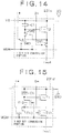
- FIG. 14 is a block diagram showing the constitution of a 1-bit D/I conversion portion according to the fourth example not part of the present invention.
- a suitable stabilized voltage VB instead of the ground potential GND is supplied to one end of the capacity element C1, similarly to the third embodiment.
- a P channel TFT T2 in place of the N channel TFT T1 in the first example is provided similarly to the second embodiment, and a power supply potential VD is supplied to the source and one end of the capacity element C1.
- the fourth example is in the form that the third example is applied to the second example, indicating that the voltage supplied to the capacity element C1 may be any voltage as long as it is stabilized, similarly to the third example.
- the fifth example not part of tne present invention will be explained.
- the constitution of the 1-bit D/I conversion portion in the first example is changed, and for example, the fifth embodiment is applied to the pixel circuit shown in FIG. 4A .
- FIG. 15 is a block diagram showing the constitution of a 1-bit D/I conversion portion according to the fifth example not part of the present invention.
- N channel transistors T11 to T13 in place of the switches SW1 to SW3 in the first example are provided.
- the operation similar to the first example is carried out on the basis of the timing chart shown in FIG. 11 , and the similar effect is obtained. It is noted that P channel transistors may be used in place of the N channel transistors T11 to T13. In this case, in the timing chart, the output signal of F/F is made to be a signal that one shown in FIG. 11 is inverted.
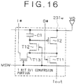
- FIG. 16 is a block diagram showing the constitution of a 1-bit D/I conversion portion according to the sixth example not part the present invention.
- N channel transistors T11 to T13 in place of the switches SW1 to SW3 in the second example are provided.
- the operation similar to the second example is carried out on the basis of the timing chart shown in FIG. 11 , and the similar effect is obtained. It is noted that P channel transistors may be used in place of the N channel transistors T11 to T13. In this case, in the timing chart, the output signal of F/F is made to be a signal that one shown in FIG. 11 is inverted.
- FIG. 17 is a block diagram showing the constitution of a semiconductor device for a light emission display device according to a seventh example not part of the present invention.
- a D/I conversion portion 210a is provided, and the D/I conversion portion 210a is provided with a shift register comprising a 1-output D/I conversion portion 230a for the outputs of (3 ⁇ n) to the light emission display device, and n flip-flops (F/F) 290a_1 to 290a_n provided every 3-output.
- a start signal IST for controlling timing for storing current
- a clock signal TCL an inverted signal ICLB of the clock signal ICL
- a current storing timing signal IT a current storing timing signal
- digital image data D0 to D2 of each output are input into the 1-output D/I conversion portion 230a, and any of reference current IR0 to IR2, IG0 to IG2, and IB0 to IB2 for reference are input according to light emitting colors assigned thereto, one F/F 290a, and three 1-output D/I conversion portions 230a into which are input signals MSW1 and MSW2 output from the F/F 290a constitute one RGB D/I conversion portion 220a.
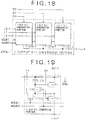
- FIG. 18 is a block diagram showing the constitution of a 1-output D/I conversion portion 230a.
- the 1-output D/I conversion portion 230a comprises three 1-bit D/I conversion portions 231f. Any of a combination of image data D0 and reference current I0, a combination of image data D1 and reference current I1, and a combination of image data D2 and reference current I2 is input into these 1-bit D/I conversion portions 231f, and signals MSW1 and MSW2 which are output signals of F/F are input.
- FIG. 19 is a block diagram showing the constitution of the 1-bit D/I conversion portions 231f.
- the 1-bit D/T conversion portions 231f is provided, similar to the fifth example, with the current storing and outputting transistor N channel TFT T1, N channel transistors T11 to T13, and the capacity element C1.
- the gradation data D0, the signal MSW2 and the signal MSW1 are input into the gates of the transistors T11, T12, and T13, respectively, and the transistors are controlled by these signals.
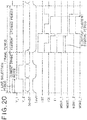
- FIG. 20 is a timing chart showing the operation of the semiconductor device for a light emission display device according to the seventh example not part of the present invention.
- the signal MSW1 changes similarly to the signal MSW1 in the first example, as shown in FIG. 20 .
- the current storing timing signal IT rises in synchronism with rising of the signals MSW1, and falls at a timing earlier than the signal MSW.
- the signal MSW2 rises at the same timing as the signal MSW1, and falls in synchronism with the falling of the current storing timing signal IT.
- the period during which the signal MSW2 rises is termed as a 3-output current storing period in the RGB D/I conversion portion 220a.
- FIG. 21 is a block diagram showing the constitution of the 1-bit D/I conversion portion in the eighth example not part of the present invention.
- a 1-bit D/I conversion portion 231q in the eighth example is provided with a P channel TFT T2 in place of the N channel TFT T1 in the seventh embodiment, and a power supply potential VD is supplied to the source thereof and one end of the capacity element C1.
- FIG. 22 is a block diagram showing the constitution of the semiconductor device for a light emission display device according to the ninth example not part of the present invention.
- a D/I conversion portion 210b is provided.
- the D/I conversion portion 210b is provided with a shift register comprising a 1-output D/I conversion portion 230b for outputs of (3 ⁇ n) to the light emission display device, and n flip-flops (F/F) 290b_1 to 290b_n provided every 3-output.
- a start signal IST for controlling timing for storing current
- a clock signal ICL an inverted signal ICLB of the clock signal ICL
- a current storing timing signal IT Into the shift register are input a start signal IST for controlling timing for storing current, a clock signal ICL, an inverted signal ICLB of the clock signal ICL, and a current storing timing signal IT.
- digital image data D0 to D2 of each output are input into the 1-output D/I conversion portion 230b, and any of reference current IR0 to IR2, IG0 to IG2, and IB0 to IB2 for reference are input according to light emitting colors assigned thereto.
- One F/F 290b. and three 1-output D/I conversion portions 230b into which are input signals MSW1, MSW2 and MSW2B output from the F/F290b constitute one RGB D/I conversion portion 220b. Note that the signal MSW2B is an inverted signal of the signal MSW2.
- FIG. 23 is a block diagram showing the constitution of the 1-output D/I conversion portion 230b.
- the 1-output D/I conversion portion 230b comprises three 1-bit D/I conversion portions 121h. Into these 1-bit D/I conversion portions 121h are input any of a combination of image data D0 and reference current I0, a combination of image data D1 and reference current I1, and a combination of image data D2 and reference current I2, and signals MSW1, MSW2 and MSW2B which are output signals of F/F are input.
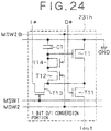
- FIG. 24 is a block diagram showing the constitution of the 1-bit output D/I conversion portion 231h.
- the 1-bit output D/I conversion portion 231h is provided, similarly to the seventh example, with the current storing and outputting transistor N channel TFT T1, N channel transistors T11 to T13 and the capacity element C1.
- Gradation data D0, a signal MSW2, and a signal MSW1 are input into the gates of the transistors T11, T12 and T13, and the transistors are controlled by these signals.
- an N channel transistor T14 is connected between the N channel transistor T12 and one end of the capacity element C1.
- the source and the drain of the N channel transistor 14 are short-circuited each other, and the signal MSW2B is input into the gate thereof.
- the gate of the TFT T1 is connected to a contact between the drain of the N channel transistor 14 and one end of the capacity element C.
- the product of Lhe transistor length L and the transistor width W of the transistor T14 is one half the product of the transistor length L and the transistor width W of the transistor T12.
- the semiconductor device for a light emission display device is operated, similarly to the seventh example, on the basis of the timing chart shown in FIG. 20 .
- a waveform of the signal MSW2B is one in which a waveform of the signal MSW2 is inverted.
- the transistor T12 is turned OFF, and simultaneously therewith, the transistor T14 is turned ON, after which the transistor T13 is turned OFF. Because of this, the gate voltage of TFT T1 in the state that reference current is caused to flow stably between the drain and the source is not affected by the noise when the transistor T13 is turned OFF, and movement of a load caused when the transistor T12 is turned ON is also absorbed by turning-ON of the transistor T14 and is held more accurately. As described above, current of higher accuracy than the seventh example can be supplied.
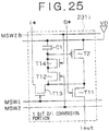
- FIG. 25 is a block diagram showing the constitution of a 1-bit D/I conversion portion according to the tenth example not part of the present invention.
- a P channel TFT T2 is provided in place of the N channel TFT T1 in the ninth example, and a power supply potential VD is supplied to the source and one end of the capacity element C1.
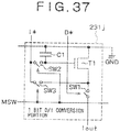
- FIG. 37 is a block diagram showing the constitution of the 1-bit D/I conversion portion in the eleventh example not part of the present invention.
- both ends of SW2 are not connected to a contact between the switch SW1 and TFTI and the gate of TFT T1, respectively, but connected to a signal line to which reference current I * is supplied and the gate of TFT T1.
- the operation of the eleventh example is similar to that of the first example, and the similar effect is obtained. Further, the change as in the second and the tenth examples with respect to the first example can be carried out.
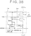
- FIG. 38 is a block diagram showing the constitution of a 1-bit D/I conversion portion according to the twelfth example.
- TFT T15 is added between TFT T1 and the GND line, and a suitable voltage VS1 is applied to the gate of TFT T15.
- the operation of the twelfth example is similar to that of the first example, and the similar effect is obtained. Further, since in the example, the added TFT T15 and TFT T1 are cascode connected, the drain voltage dependability of drain current in the saturated area of TFT1 is flattened to enable improving accuracy of output current Iout. In addition, the present example is able to carryout the change as in the second to the tenth examples with respect to the first embodiment.
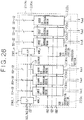
- FIG. 26 is a block diagram showing the constitution of the semiconductor device for a light emission display device according to the eleventh example not part of the present invention.
- a D/I conversion portion 210c is provided.
- the D/I conversion portion 210c is provided with a shift register comprising a 1-output D/T conversion portion 230c for outputs of (3 ⁇ n) to the light emission display device, and n flip-flops (F/F) 290_1 to 290_n.
- a start signal IST for controlling timing for storing current
- a clock signal ICL for controlling timing for storing current
- ICLB of the clock signal ICL is input.
- digital image data D0 to D2 of each output are input into the 1-output D/I conversion portion 230c, and any of reference current IR2, IG2, and IB2 for reference current are input according to light emitting color assigned thereto.
- One F/F290 and three 1-output D/I conversion portions 230c into which is input a signal MSW output from the F/F290 constitute one RGB D/I conversion portion 220c.
- the current values or reference current are adjusted to the current brightness characteristics in which light emitting colors are red, blue, and green.
- a current value ir2 of reference current IR2 corresponds to the fourth gradation in which light emitting color is red
- a current value ig2 of reference current IG2 corresponds to the fourth gradation in which light emitting color is green
- a current value ib2 of reference current IB2 corresponds to the fourth gradation in which light emitting color is blue. That is, reference current supplied to the 1-output D/I conversion portion 230c for displaying red (R) is reference current IR2 corresponding to brightness of the fourth gradation of the luminous element for displaying red.
- reference current IG2 or IB2 is input into the 1-output D/I conversion portion 230c for displaying green (G) or blue (B). Accordingly, in the present example, the minimum value of reference current input is four times of that of the first example.
- FIG. 27 is a block diagram showing the constitution of the 1-output D/I conversion portion 230c.
- the 1-output D/I conversion portion 230c is provided with a switch SW23a controlled by a signal MSW and to one end of which is supplied reference current I*.
- a drain and a gate of an N channel TFT T23 are connected in common to the other end of the switch 23a.
- a source of TFT T23 is grounded.
- One end of a switch SW23b controlled by signal MSW is connected to the drain and the gate of the N channel TFT T23, and gates of N channels TFT T20 to T22 and one end of the capacity element C2 axe connected in common to the other end thereof.
- the sources of TFT T20 to T22 and the other end of the capacity element C2 are grounded.
- Switches SW20, SW21 and SW22 controlled by gradation data D0, D1 and D2, respectively, are connected to the drains of TFT T20, T21 and T22, and the other ends of these switches SW20 to SW22 are connected in common.
- Output current Iout is output from the common connected point.
- the current ability ratio of TFT T20, T21 and T22 is 1 : 2 : 4.
- the current ability of TFT T22 and the current ability of TFT T23 are designed to be the same each other.
- a voltage higher than a ground potential GND instead of the ground potential GND may be supplied to the sources of TFT T20 to T23 and one end of the capacity element C2.
- the capacity element C2 may be connected to a different signal line.
- the semiconductor device for a light emission display device operates, similarly to the first example, on the basis of the timing chart shown in FIG. 11 .
- each 1-output D/I conversion portion 230c stores reference current (either IR2, IG2 or IB2) supplied from the reference current source.
- reference current either IR2, IG2 or IB2
- all digital gradation data are a low level, and the switches SW20 to SW22 of the 1-output D/I conversion portion 230c are OFF.
- a pulse signal as the start signal IST is input into F/F 290_1 of the first stage, and simultaneously with the input of the pulse signal, a clock signal ICL and a clock inverted signal ICLB are input into F/F 290_1 whereby a shift register comprising n F/F 290 begins to operate.
- an output signal MSW_1 of F/F 290_1 of the first stage assumes a high level, switches SW23a and SW23b provided in the 1-output D/I conversion portion 230c within the RGB D/I conversion portion 220c provided with the F/F 290_1 are turned ON.
- the current storing TFT T23 of the 1-output D/I conversion portion 230c operates in a saturated area since a portion between the gate and the drain thereof is short-circuited. Thereafter, the gate voltage (of TFT T23) is set adjusting to the current/voltage characteristics of TFT T23 so that reference current from the reference current source flows between the drain and the source of TFT T23 in the stabilized condition.
- the switches SW23a and SW23b of the 1-output D/I conversion portion 220c provided with F/F 290_1 are turned OFF.
- a voltage so that TFT T23 causes reference current to flow is held by the capacity element C2 of the 1-output RGB D/I conversion portion 230 within the RGB D/I conversion portion 220c provided with F/F 290_1.
- the outputting TFT T20 to T22 are able to flow, corresponding to the current ability ratio with respect to TFT T23, current corresponding to the first gradation, current corresponding to the second gradation, and current corresponding to the fourth gradation.
- the period in which the signal MSW is at a high level as described is termed as a 3-output current storing period in the RGB D/I conversion portion 220c.
- the switches SW23a and SW23b within the RGB D/I conversion portion 220c provided with F/F of the second stage are turned ON, and in the stabilized condition, operation is made in a saturated area so that reference current flows between the drain and the source of TFT T23, and the gate voltage is set adjusting to the current/voltage characteristics of TFT T23 so that reference current flows.
- the 3-output current storing period as mentioned above is repeated with respect to all RGB D/I conversion portions 220c, and reference current is stored in all 1-output D/I conversion portions 230c.
- the vertical scanning circuit 300 selects control lines line by line.
- a control line of the first line is selected, and in synchronism therewith, 3-bit digital gradation data D0 to D2 of the first line corresponding to outputs are input into the 1-output D/I conversion portion 230c every output.
- the digital gradation data D0 to D2 are input, turning ON/OFF if switches SW20 to SW22 is controlled according to these levels (high level (H)/low level (L)), and current having been stored in the current driving period of the frame immediately before is output according to current ability of TFT T20 to T22.
- gradation expression as shown in Table 1 becomes enabled.
- the output current value can be adjusted, from 0 to 7 x i0, by digital gradation data input. Further, reference current is stored adjusting to unevenness of current/voltage characteristics in the current storing period (the second operation period), and in a close area, the unevenness of current/voltage characteristics is small. Therefore, unevenness of current is small irrespective of unevenness of current/voltage characteristics in a large area, and high accuracy is obtained.
- the shift register is not operated, and all switches SW23a and SW23b always remain turned OFF.
- reference current is four times of the minimum value of reference current in the first example, charging and discharging of a load of wiring for flowing reference current can be carried out at high speed, and it is possible to attain a stabilized condition quickly. Accordingly, since the current storing period can be shortened to extend the current driving period, current of higher accuracy can be supplied to the pixel within the display portion.
- the polarity of the transistor may be changed; a transistor may be used as a switch; and timings for turning OFF the switches SW23a and SW23b may deviated each other or transistors are added to raise accuracy of output current.
- current ability of TFT T23 is made larger than current ability of TFT T22 whereby the minimum value of reference current can be made larger.
- the charting and discharging time for a load of a wiring to the pixel within the display portion can be secured longer, and current of higher accuracy can be supplied to the pixel.
- FIG. 28 is a block diagram showing the constitution of a 1-bit D/I conversion portion according to the fourteenth example.
- TFT T23 is not provided, and one end of the switch SW 23a is connected to a drain of TFT T22. Further, the switch SW 23b is connected between the drain and the source of TFT T22.
- the current value of reference current is adjusted to the current brightness characteristics in which light emitting colors are red, blue and green; and the current value ir2 of reference current IR2 corresponds to the fourth gradation in which light emitting color is red, the current value ig2 of reference current IG2 corresponds to the fourth gradation in which light emitting color is green, and the current value ib2 of reference current IB2 corresponds to the fourth gradation in which light emitting color is blue. That is, the reference current supplied to the 1-output D/I conversion portion 230d for displaying red (R) is reference current IR2 corresponding to brightness of the fourth gradation of a luminous element for displaying red.
- reference current IG2 or IB2 is input into the 1-output D/I conversion portion 230c for displaying green (G) or displaying blue (B). Accordingly, in the present example, the minimum value of reference current input will be 4 times of that of the first example.
- the reason for causing the reference current to correspond to the fourth gradation is that as will be mentioned later, design was made so that current ability of outputting TFT T20, T21 of the 1-output D/I conversion portion 230d and current ability of TFT T22 for storing and outputting current are 1 : 2 : 4.
- the semiconductor device for a light emission display device according to the fourteenth example constituted as described above is also operated on the basis of the timing chart shown in FIG. 11 , similarly to the first example.
- each 1-output D/I conversion portion 230d stores reference current (either IR2. IG2 or IB2) supplied from the reference current source.
- reference current either IR2. IG2 or IB2
- all digital gradation data are made to be a low level, and the switches SW20 to SW22 of the 1-output D/I conversion portion 230d are turned OFF.
- a pulse signal as a start signal IST is input into F/F 290_1 of the first stage, and simultaneously with the input of the pulse signal, a clock signal ICL and a clock inverted signal ICLB are input into F/F 290_1 whereby a shift register comprising n F/F290 begins to operate.
- an output signal MSW_1 of F/F 290_1 of the first stage assumes a high level, switches SW23a and SW23b provided in the 1-output D/I conversion portion within the RGB D/I conversion portion 220c provided with the F/F 290_1 are turned ON.
- the current storing and outputting TFT T22 of the 1-output D/I conversion portion 230d operates in a saturated area because a portion between the gate and the drain is short-circuited. Thereafter, in the stabilized condition, the gate voltage is set adjusting to the current/voltage characteristics of TFT T22 so that reference current from the reference current source flows between the drain and source of TFT T22.
- the outputting TFT T20 to T22 are able to flow, corresponding to the current ability ratio, current corresponding to the first gradation, current corresponding to the second gradation, and current corresponding to the fourth gradation.
- the period in which the signal MSW is at a high level as described above is termed as a 3-output current storing period in the RGB D/I conversion portion 220c.
- the switches SW23a and SW23b within the RGB D/I conversion portion 220c provided with F/F of the second stage are turned ON, and in the stabilized condition, operation is made in a saturated area so that reference current flow between the drain and the source of TFT T22, and the gate voltage is set adjusting to the current/voltage characteristics of TFT T22 so that the reference current flows.
- the 3-output current storing period as described above is repeated with respect to all RGB D/I conversion portions 220c, and reference current is stored in all 1-output D/I conversion portions 230d.
- the vertical scanning circuit 300 selects the control lines line by line.
- the control line of the first line is selected, and in synchronism therewith, 3-bit digital gradation data D0 to D2 of the first line corresponding to outputs are input into the 1-output D/I conversion portion 230d every output.
- the digital gradation data D0 to D2 are input, turning ON/OFF of the switches SW20 to SW22 is controlled according to these levels (high level (H)/low level (L)), and current having been stored in the current driving period of the frame immediately before is output according to the current ability of TFT T20 to T22.
- gradation expression as shown in Table 1 results.
- the output current value can be adjusted, from 0 to 7 x i0, by digital gradation data input. Further, reference current corresponding to the fourth gradation is stored adjusting to unevenness of current/voltage characteristics in the current storing period (the second operation period), and current corresponding to the fourth gradation in TFT T22 is output, because of which current of high accuracy can be output as current corresponding to the fourth gradation.
- current output in TFT T20 and T21 correspond to the first gradation and the second gradation, respectively, but current values thereof are not more than one half of current of the fourth gradation, and even if the current value is varied due to the unevenness of current/voltage characteristics, its influence is small as compared with the case where the fourth gradation is uneven.
- the shift register is not operated, and all switches SW23a and SW23b always remain turned OFF.
- reference current is four times of the minimum value of reference current in the first example
- charging and discharging of a load of wiring for flowing reference current can be carried out at high speed, and it is possible to attain a stabilized condition quickly. Accordingly, since the current storing period can be shortened to extend the current driving period, the charging and discharging time for a load in a wiring to the pixel within the display portion can be secured long. Because of this, current of higher accuracy can be supplied to the pixel.
- the polarity of the transistor may be changed; a transistor may be used as a switch; and timings for turning OFF the switches SW23a and SW23b may deviated each other or transistors are added to raise the accuracy of output current.
- arrangement is made so that only the TFT T22 is a transistor for storing and outputting current but TFT T21 also stores and outputs current to increase reference current whereby even where the close area is uneven, current of higher accuracy can be supplied.
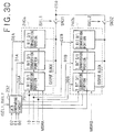
- FIG. 29 is a block diagram showing the constitution of a semiconductor device for a light emission display device according to the fifteenth example of the present invention.
- a D/I conversion portion 210d is provided with a shift register comprising a 1-output D/I conversion portion 230e for outputs of (3 x n) to the light emission display device and n flip-flops (F/F) 290c_1 to 290c_n provided every 3-output.
- a start signal IST for controlling timing for storing current
- a clock signal ICL for controlling timing for storing current
- ICLB inverted signal
- ISEL1 current selector signal
- digital image data D0 to D2 are input into the 1-output D/I conversion portion 230e, and any of reference current IR0 to IR2, IG0 to TG2, and IB0 to IB2 is input according to light emitting colors assigned thereto.
- Reference current has a current value adjusted to the current-brightness characteristics of luminous elements in which light emitting colors are red, blue, and green, and a current value ir0 of reference current IR0 corresponds to the first gradation of a luminous element whose light emitting color is red, a current value ir1 of reference current IR1 corresponds to the second gradation of a luminous element whose light emitting color is red, and a current value ir2 of reference current IR2 corresponds to the fourth gradation of a luminous element whose light emitting color is red.
- a current value ir0 of reference current IR0 corresponds to the first gradation of a luminous element whose light emitting color is red
- a current value ir1 of reference current IR1 corresponds to the second gradation of a luminous element whose light emitting color is red
- a current value ir2 of reference current IR2 corresponds to the fourth gradation of a luminous element
- current values of reference current IG0 to IG2 correspond to the first gradation, the second gradation and the fourth gradation whose light emitting color is green, respectively
- current values of reference current IB0 to IB2 correspond to the first gradation, the second gradation and the fourth gradation whose light emitting color is blue, respectively.
- current selector signals ISEL1 and ISEL2 are input into the 1-output D/I conversion portion 230e.
- One F/F 290c, and three 1-output D/I conversion portions 230e into which signals MSWA and MSWB output from the F/F290c constitute one RGB D/I conversion portion 220d.
- FIG. 30 is a block diagram showing the constitution of a 1-output D/I conversion portion 230e.
- the 1-output D/I conversion portion 230e is provided with output blocks 240a and 240b respectively comprising three 1-bit D/I conversion portions 231 and a data preparation circuit 232. Further, there are provided switches SW31 and SW32 controlled by current selector signals ISEL1 and ISEL2, respectively, and for selecting if current is output from which block out of the output blocks 240a and 240b.
- the data preparation circuit 232 produce data signals D0A to D2A and D0B to D2B on the basis of digital gradation data E0 and D2 for 1-output and the current selector signals ISEL1 and ISEL2.
- the data signals D0A to D2A are input into the output block 240a, and the data signals D0B to D2B are input into an output block 240_2.
- An output signal MSWA of F/F 290c is input into the output block 240a, and an output signal MSWB of F/F 290c is input into the output block 240b.
- Reference current I0 to I2 for reference are input into the output blocks 240a and 240b.
- gradation data D0, D1 and D2 are input reference current IG0 or IB0, reference current IG1 or IB1, and reference current IG2 or IB2, respectively.
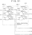
- FIG. 31 is a circuit view showing the constitution of one example of the data preparation circuit 232.
- the data preparation circuit 232 is provided with NAND gates NAND0A to NAND2A with the current selector signal ISEL1 as 1 input, for example, inverters IV0A to IV2A for inverting these outputs, NAND gates NAND0B to NAND2B with the current selector signal ISEL2 as 1 input, and inverters IV0B to IV2B for inverting these outputs.
- Gradation data D0 is further input into the NAND gates NAND0A and NAND0B
- gradation data D1 is further input into the NAND gates NAND1A and NAND1B
- gradation data D2 is further input into the NAND gates NAND2A and NAND2B.
- data signals D0A to D2A and D0B toD2B are output from the inverters IV0A to IV2A and IV0B to IV2B, respectively.
- this constitution is one example, and other constitutions may be employed if a similar signal can be output.
- FIG.32 is a timing chart showing the operation of the semiconductor device for a light emission display device according to the fifteenth example.
- a period from the beginning of vertical scanning of the display portion 400 (see FIG. 1 ) to the beginning of the next vertical scanning is termed as 1 frame.
- two kinds of frames in which one of the mutually exclusive current selector signals ISEL1 and ISEL2 assumes a high level appear alternately.
- the current selector signal ISEL1 assumes a high level
- the current selector signal ISEL2 assumes a low level.
- the switch SW1 is turned ON to output current.
- the switch SW2 is turned OFF to store current.
- the 1-bit D/I conversion portion 231 within the output block 240b stores any one of reference current IR0 to IR2, IG0 to IG2, and IB0 to IB2.
- the digital gradation data DB0 to DB2 are at a low level
- the switch SW1 of the 1-bit D/I conversion portion 231 within the output block 240b is OFF.
- a pulse signal as a start signal IST is input into F/F 290c_1 of the first stage, and a clock signal ICL and a clock inverted signal ICLB are input into F/F 290c_1 simultaneously with the input of the pulse signal whereby a shift register comprising n F/F 290 starts to operate.
- switches SW2 and SW3 of each 1-bit D/I conversion portion 231 of the output block 240b provided in the 1-output D/I conversion portion 230e into which the output signal MSWB_1 is input are turned ON.
- the period in which the signal MSW is at a high level is termed as a 3-output current storing period in the RGB D/I conversion portion 220d.
- the switches SW2 and SW3 of the output block 240b within the RGB D/I conversion portion 220d provided with F/F of the second stage are turned ON, and in the stabilized condition, operation is carried out in a saturated area so that reference current flows between the drain and the source of TFT T1 of the 1-bit D/I conversion portion 231, and the gate voltage is set adjusting the current/voltage characteristics of TFT T1 so that reference current flows.
- the 3-output current storing period as mentioned above is repeated with respect to the second output block 240b within all the RGB D/I conversion portions 220d, and reference current is stored in the second output block 240b of all the 1-output D/I conversion portions 230e.
- the vertical scanning circuit 300 selects control lines line by line.
- FIG. 32 shows scanning pulses Y_1 and Y_2 which are outputs of the first line and the second line, respectively.
- the control line of the first line is selected, and in synchronism therewith, 3-bit digital gradation data D0 to D2 of the first line corresponding to outputs are input into the first output block 240a within the 1-output D/I conversion portion 230e every output.
- the digital gradation data D0 to D2 are input, turning ON/OFF of the switch SW1 within the 1-bit D/I conversion portion 231 is controlled according to these level (high level (H)/low level (L)), and current having been stored in TFT T1 in the current driving period of the frame immediately before whereby gradation expression is carried out.
- the output current value can be adjusted, from 0 to 7 x i0, by digital gradation data input. Further, in the frame immediately before, the gate voltage is set so that current equal to the reference current source flows adjusting to the current/voltage characteristics of TFT T1, and being output using the same TFT T1, because of which unevenness of output current is small, irrespective of the unevenness of current/voltage characteristics, and high accuracy is obtained.
- the output MSWA of the shift register is always at a low level, and the switches SW2 and SW3 within all the output blocks 240a always remain turned OFF.
- the current selector signal ISEL1 is set to a low level, and the current selector signal ISEL2 is set to a high level, whereby the operation of the first output block 240a is replaced with the operation of the second output block 240b.
- the first output block 240a stores current
- the second output block 240b outputs current.
- the above-described operation is repeated every 2 frames, whereby current of high accuracy can be supplied to the pixel circuit.
- two output blocks are provided in 1-output, in each frame, one output block can be used to output current, and the other output block can be used to store current, and the current storing period need not be provided separately.
- one frame period serves as a current driving period, the charging and discharging time for a load of a wiring to the pixel within the display portion can be secured longer. Accordingly, current with higher accuracy can be supplied to the pixel.
- a period of current storage is not limited to every one frame, but may be every several frames.
- the period of current storage is set every several frames whereby a period of current storage is extended, and therefore, current can be stored with higher accuracy.
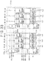
- FIG. 33 is a block diagram showing the constitution of the semiconductor device for a light emission display device according to the first embodiment of the present invention.
- a D/I conversion portion 210e is provided.
- the D/I conversion portion 210e has the constitution similar to that of the D/I conversion portion 210d in the first embodiment except that a precharge circuit 250 is provided at the rear of each 1-output D/I conversion portion 230e.
- a precharge signal PC is input into the precharge circuit 250.
- FIG. 34 is a current diagram showing the constitution of the precharge circuit 250.
- the precharge circuit 250 is provided with N channel transistors T31 to T33 controlled by the precharge signal PC and a P channel transistor T34.
- Output current IOUT is input into one end of the transistors T31 and T32 from the 1-output D/I conversion portion, and a false load circuit 252 and a non-inverted input terminal of an ope-amp 251 are connected to the other end of the transistor T31.
- one end of the transistor T33 is connected to the transistor T31, and a gate of the P channel transistor T35 is connected to the other end of the transistor T33.
- a voltage VEL is supplied to a source of the transistor T35, and the other end thereof is connected to the transistor T31.
- An output signal of the ope-amp 251 itself is input into an inverted input terminal of the ope-amp 251, one end of the transistor T32 is connected to an output terminal of the ope-amp 251, and the other end thereof is connected to the other end of the transistor T34.
- a driving current of a luminous element is output from a common connection between the transistors T32 and T34.
- the false load circuit 252 may be a constitution in which the gate and the drain of the transistor T35 is short-circuited, and the transistor T33 is not provided. Further, since the transistors T31, T32 and T34 act as a switch, a transistor of reverse polarity may be used according to the polarity of the precharge signal PC, for example, and if a constitution is employed in which the precharge signal PC itself and its inverted signal are input, transistor of any polarity can be used.
- FIG. 35 is a timing chart showing the operation of the precharge circuit 250.
- a 1 line selection period is divided into a first period and a second period according to a level of the precharge signal PC.
- the precharge signal PC is at a high level, which period is a precharge period.
- a scanning pulse Y_1 assumes a high level
- a control line of the first line is selected, in synchronism with which 3-bit digital gradation data D0 to D2 of the first line corresponding to outputs are input into the 1-output D/I conversion portion 230e every output.
- the 1-output D/I conversion portion 230e outputs current in accordance with the relationship shown in Table 1 from the digital gradation data DA0 to DA2 input.
- the precharge signal PC is at a high level
- the transistor T34 within the precharge circuit 250 is turned OFF, and the transistors T31 and T32 are turned ON.
- the precharge circuit 250 output current of the 1-output D/I conversion portion 230e flows into the false load circuit 252. Since the false load circuit 252 is provided with the transistor T35, where output current Iout flows in a stabilized manner, the gate voltage of the transistor T35 is substantially the same voltage as the gate voltage where the output current Iout flows into the pixel circuit within the display portion in a stabilized manner. And, this voltage will be an input of the voltage follower constituted by the ope-amp 251, and in the precharge period, the transistor T32 is turned ON, because of which output of the voltage follower will be output of the D/I conversion portion 210e. Thereby, in the present period, the gate voltage of the transistor T35 can be applied to the pixel circuit within the display portion.
- the false load circuit 252 is located close to the 1-output D/I conversion portion 230e away from the pixel circuit, and a wiring load or the like which need be charged or discharged is extremely small. Therefore, the operation for flowing constant output current of the 1-output D/I conversion portion 230e into the transistor T35 in a stabilized manner can be carried out at very high speed, even where output current value is low, as compared with the case where the pixel circuit within the display portion is driven by constant output current of the 1-output D/I conversion portion 230e. Further, the operation for applying the gate voltage of the transistor T35 to the pixel circuit within the display portion can be also realized because the operation is carried out by output of low impedance which is a voltage follower.
- the precharge signal is at a low level, and the period is a current output period.
- the precharge signal PC is at a low level
- the transistor T34 within the precharge circuit 250 is turned ON, and the transistors T31 and T32 are turned OFF. Therefore, in the precharge circuit 250, output current of the 1-output D/I conversion portion 230e is output without modification, and the pixel circuit within the display portion is driven.
- the precharge operation is carried out in the first period, and therefore, a voltage close to that where output current of the 1-output D/I conversion portion 230e flows in a stabilized manner is applied to the pixel circuit within the display portion.
- the operation for correcting unevenness of current ability between the transistor T35 and the transistor TFT T102 ( FIG. 4 ) in the pixel circuit within the display portion, and the operation for flowing output current lout to the pixel circuit within the display portion in a stabilized manner to drive it are carried out.
- the amount for charging and discharging the wiring load or the like in the second period will suffice to be small.
- the period can be shortened as compared with the case where the precharge operation is not carried out. Further, since the current driving is carried out after a stable voltage has been output by the precharge operation, the operation becomes enabled without being affected by the condition prior to the 1 line selection period.
- the scanning pulse Y_1 assumes a low level
- the scanning pulse Y_2 assumes a high level
- the control line of the second line is selected, and the same operation is repeated.
- first to fifteenth examples may be applied as the 1-output D/I conversion portion of the first embodiment, and if it apply the circuit/semiconductor device which supply current are not included in the present invention, similar effect can be obtained.
- FIG. 36 is a block diagram showing the constitution of a precharge circuit according to the second embodiment.
- An N channel transistor T36 into which the precharge signal PC is input and P channel transistors T37 and T38 are provided in the precharge circuit 250a in the second embodiment in addition to the constitutional elements of the precharge circuit 250.
- the transistor T38 is connected between an output terminal of the ope-amp 251 and an inverted input terminal. Further, a capacity element C3 is input into an output terminal of the ope-amp 251, the transistor T36 is connected between the other end thereof and the inverted input terminal, and the transistor T37 is connected between it and a non-inverted input terminal.
- the thus constituted precharge circuit 250a is provided with a circuit for canceling an offset voltage of the ope-amp 251 well known, and the offset canceling operation is carried out in a current driving period whereby the precharge operation can be carried out without being affected by the offset voltage of the ope-amp 251.
- Other operations are similar to the operation of the precharge circuit 250 in the first embodiment.
- FIG. 39 shows the sixteenth example not part of the present invention.
- the sixteenth example provides a horizontal driving circuit 200 comprising a data register 203 for holding a digital signal to be input, a data shift register 202 for outputting a scanning signal in synchronism with the holding timing, a data latch 204 for holding signals of all data registers in synchronism with a latch signal to output them to a D/I conversion portion 210, and a D/I conversion portion 210 for outputting current in accordance with the digital data signals.
- the D/I conversion portion 210 may include a precharge circuit. Further, the D/I conversion portion 210 may be constituted by the D/I conversion portion in any of the first to fifteenth examples and first to second embodiments of the present invention.
- FIG. 40 shows the seventeenth example not part embodiment of the present invention.
- outputs of the D/I conversion portion of the sixteenth example can be connected sequentially to a plurality of display portions 400 by a selector circuit 211 to thereby increase data lines and pixel circuits that can be driven without increasing circuit scales.
- FIG. 41 shows the eighteenth example not part of the present invention.
- a reference current source 212 for preparing reference current is encased in a horizontal driving circuit 200, in the eighteenth embodiment.
- a transistor is explained referring to TFT, but a more general transistor may be employed, and a plurality of horizontal driving circuits 200 may be used with respect to a single display portion. Further, all transistors are prepared by TFTs whereby the display portion 400, the horizontal driving circuit 200 and the vertical scanning circuit 300 may be formed on the same substrate.
- a load (circuit) of the precharge circuit in the embodiment of the present invention is prepared by a load (circuit) having the same constitution as the load of the display portion 400 to enable realizing precharging of higher accuracy.
- the light emission display device provided with the luminous element in which the current-brightness characteristics are in a proportional relationship in colors (R, G, B) has been explained referring to the example of the device which is driven in 4096 color display for which 3-bit digital gradation data of 0 gradation to 7 gradations display.
- the similar constitution can be extended without modification.
- all transistors are of TFTs, but even more general transistors, the present invention can be realized by the similar constitution.
- the active matrix type pixel circuit there is supposed FIG. 4A , but also with respect to the pixel circuits of other current driving system and even with respect to the pixels the simple matrix system, the present invention can be realized by the similar constitution.
- current of high accuracy can be supplied to a cell (circuit) of the current load device. This is because of the fact that a voltage between the gate and the source in the state that reference current flows in a stabilized manner between the drain and source of the transistor within the digital-to-current conversion device is stored whereby current of high accuracy can be stored, without being affected by the unevenness of current/voltage characteristics of the transistors, and current is output by the transistor having current stored therein. Further, the number of transistors for storing and outputting current can be increased or decreased in accordance with the unevenness of current/voltage characteristics in the close area.
- the time for storing can be shortened, and the time for outputting (driving) is extended t ⁇ enable securing the time for charging and discharging the data line within the current load device and the load of the pixel longer. Accordingly, current of higher accuracy can be supplied to the cell (circuit) of the current load device. Further, the transistor for storing current every output terminal and the transistor for outputting current are provided every output terminal, and are replaced every frame, whereby the storing period is not necessary separately, and the time for outputting (driving) can be extended. As a result, current of higher accuracy can be supplied to the cell (circuit) of the current load device.
- the precharge circuit provided with the false load circuit is provided between the output of the digital-to-current conversion device and the current load device whereby even where the output current value is low, current or the pixel (circuit) of the device can be driver at high speed.
- the false load circuit is driven at high speed by the current output of the digital-to-current conversion device, the voltage obtained from the false load circuit is supplied to the cell (circuit) within the current load device by the voltage follower, and the voltage where the current output of the digital-to-current conversion device is applied to the cell (circuit) within the current load device can be applied at high speed, after which the cell (circuit) within the current load device is directly driven by the current output of the digital-to-current conversion device to correct it, which operation is carried out whereby the amount of charging and discharging with constant current of loads of the pixel within the current load device or the signal line can be reduced.
Landscapes
- Engineering & Computer Science (AREA)
- Physics & Mathematics (AREA)
- Computer Hardware Design (AREA)
- General Physics & Mathematics (AREA)
- Theoretical Computer Science (AREA)
- Control Of Indicators Other Than Cathode Ray Tubes (AREA)
- Control Of El Displays (AREA)
- Electroluminescent Light Sources (AREA)
Claims (14)
- Halbleitergerät, das zum Treiben eines Stromverbrauchergeräts ausgelegt ist, das mit einer Vielzahl von Steuerleitungen (110) und einer Vielzahl von Zellen bereitgestellt ist, die ein Stromverbraucherelement aufweisen, umfassend:eine Vielzahl von Stromausgabeschaltungen, die zum Ausgeben eines Ausgangsstroms (I OUT) konfiguriert ist;eine Vielzahl von Vorladeschaltungen (250, 250a), wobei jede der Vorladeschaltungen (250, 250a) elektrisch mit einer der Stromausgabeschaltungenverbunden ist und jede der Vorladeschaltungen (250, 250a) eine falsche Verbraucherschaltung (252) und einen Spannungsfolger umfasst;
wobei eine Auswahlperiode von einer der Steuerleitungen (PC) eine erste Periode und eine zweite Periode umfasst, wobei die Stromausgabeschaltung den Ausgangsstrom (I OUT) von der entsprechenden Stromausgabeschaltung an die falsche Verbraucherschaltung (252) ausgibt und während der zweiten Periode die Stromausgabeschaltung den Ausgangsstrom (I OUT) über eine entsprechende Signalleitung an das Stromverbraucherelement in dem Stromverbrauchergerät ausgibt;dadurch gekennzeichnet, dass jede der Vorladeschaltungen (250, 250a) mit einem ersten Transistor (T34) bereitgestellt ist, der durch ein Vorladesignal (PC) gesteuert wird;ein erstes Ende des ersten Transistors (T34) das Vorladesignal (PC) empfängt, ein zweites Ende des ersten Transistors (T34) den Ausgangsstrom (I OUT) empfängt, und ein drittes Ende des ersten Transistors (T34) mit dem Stromverbrauchergerät verbunden ist;wobei jede der Vorladeschaltungen (250, 250a) weiter einen zweiten Transistor (T31) bereitstellt, der durch das Vorladesignal (PC) gesteuert wird, wobei ein erstes Ende des zweiten Transistors (T31) das Vorladesignal (PC) empfängt und ein zweites Ende des zweiten Transistors (T31) den Ausgangsstrom (I OUT) empfängt und ein drittes Ende des zweiten Transistors (T31) mit der falschen Verbraucherschaltung (252) verbunden ist;wobei während der ersten Periode das Vorladesignal (PC) den ersten Transistor (T34) zum Ausschalten und den zweiten Transistor (T31) zum Einschalten steuert, wodurch der Ausgangsstrom (I OUT) in die falsche Verbraucherschaltung (252) eingegeben wird;wobei während der zweiten Periode das Vorladesignal (PC) den ersten Transistor (T34) zum Einschalten und den zweiten Transistor (T31) zum Ausschalten steuert, wodurch der Ausgangsstrom (I OUT) in das Stromverbrauchergerät eingegeben wird. - Halbleitergerät nach Anspruch 1, dadurch gekennzeichnet, dass die Vorladeschaltung (250, 250a) einen Aufbau zum Aufheben einer Offsetspannung des Spannungsfolgers aufweist.
- Halbleitervorrichtung nach Anspruch 2, dadurch gekennzeichnet, dass eine Operation zum Aufheben der Offsetspannung des Spannungsfolgers in der Vorladeschaltung (250, 250a) einmalig in einem Frame oder einigen wenigen Frames ausgeführt wird.
- Halbleitergerät nach Anspruch 1, dadurch gekennzeichnet, dass die Stromausgabeschaltung eine n-Bit-Digital-zu-Strom-Umwandlungsschaltung (210, 210a-210d) ist.
- Halbleitergerät nach einem der Ansprüche 1 und 2-4, dadurch gekennzeichnet, dass die Vorladeschaltung (250, 250a) einen ersten Verbraucher umfasst, wobei jede der Zellen einen zweiten Verbraucher umfasst, wobei der erste Verbraucher im Wesentlichen den gleichen Aufbau wie der zweite Verbraucher aufweist.
- Halbleitergerät nach Anspruch 5, wobei das Stromverbraucherelement ein Leuchtelement ist.
- Halbleitergerät nach Anspruch 5, wobei das Stromverbraucherelement ein organisches EL-Element ist.
- Halbleitergerät zum Treiben eines Stromverbrauchergeräts nach Anspruch 1, wobei das Stromverbrauchergerät weiter eine Vielzahl von Signalleitungen (120) bereitstellt, wobei das Stromverbraucherelement durch TFT (T100) gesteuert wird.
- Halbleitergerät nach Anspruch 8, wobei das Stromverbrauchergerät weiter einen Schalter (SW100) umfasst und der Schalter (SW100) mit dem Stromverbraucherelement, der Signalleitung (120) und der Steuerleitung (110) verbunden ist; wobei ein Kapazitätselement (C100) mit dem Schalter (SW100) und dem TFT (T100) verbunden ist.
- Halbleitergerät nach Anspruch 1, wobei das Stromverbrauchergerät weiter eine Vielzahl von Signalleitungen (120) bereitstellt, wobei das Stromverbrauchergerät weiter einen ersten Schalter (SW101), einen zweiten Schalter (SW102), einen ersten TFT (T101) und einen zweiten TFT (T102) umfasst; nopewobei der zweite Schalter (SW102) mit der Signalleitung (120) und der Steuerleitung (110) verbunden ist; wobei ein Gate und ein Drain des zweiten TFT (T102) über den Schalter (SW102) mit der Signalleitung (120) verbunden sind; wobei der erste Schalter (SW101) mit der Steuerleitung (110) verbunden ist, ein Gate des ersten TFT (T101) mit dem ersten Schalter (SW101) verbunden ist, Quellen des ersten und zweiten TFT (T101, T102) mit einem Potential (VEL) verbunden sind, ein Drain des ersten TFT (T101) mit dem Stromverbraucherelement verbunden ist; ein Ende eines Kapazitätselements (C100) zwischen dem ersten und zweiten TFT (T101, T102) verbunden ist, und ein anderes Ende des Kapazitätselements (C100) mit dem Potential (VEL) verbunden ist.
- Halbleitergerät nach Anspruch 1, wobei das Stromverbrauchergerät weiter eine Vielzahl von Signalleitungen (120) bereitstellt, wobei das Stromverbrauchergerät weiter einen ersten Schalter (SW101), einen zweiten Schalter (SW102), einen dritten TFT (T103) und einen vierten TFT (T104) umfasst; wobei der zweite Schalter (SW102) mit der Signalleitung (120) und der Steuerleitung (110) verbunden ist; wobei ein Gate und ein Drain des vierten TFT (T104) über den zweiten Schalter (SW102) mit der Signalleitung (120) verbunden sind; wobei der erste Schalter (SW101) mit der Steuerleitung (110) verbunden ist, ein Gate des dritten TFT (T103) mit dem ersten Schalter (SW101) verbunden ist, Quellen des dritten und vierten TFT (T103, T104) mit einem Massepotential (GND) verbunden sind, ein Drain des dritten TFT (T103) mit dem Stromverbraucherelement verbunden ist; ein Ende eines Kapazitätselements (C100) zwischen dem dritten und vierten TFT (T103, T104) verbunden ist, und ein anderes Ende des Kapazitätselements (C100) mit dem Massepotential (GND) verbunden ist.
- Halbleitergerät nach Anspruch 1, wobei die Vorladeschaltungen (250, 250a) weiter einen dritten Transistor (T32) bereitstellen, wobei der Spannungsfolger einen Operationsverstärker (251) umfasst; wobei die falsche Verbraucherschaltung (252) und ein nicht invertierter Eingangsanschluss des Operationsverstärkers (251) mit dem dritten Ende des zweiten Transistors (T31) verbunden sind, wobei ein Ausgangssignal des Operationsverstärkers (251) selbst in einen invertierten Eingangsanschluss des Operationsverstärkers (251) eingegeben wird, wobei ein Ende des dritten Transistors (T32) mit einem Ausgangsanschluss des Operationsverstärkers (251) verbunden ist und ein erstes Ende des dritten Transistors (T32) das Vorladesignal (PC) empfängt, wobei die falsche Verbraucherschaltung (252) mit dem ersten Ende des dritten Transistors (T32) verbunden ist, ein drittes Ende des dritten Transistors (T32) und das dritte Ende des ersten Transistors (T34) mit dem Stromverbraucherelement in dem Stromverbrauchergerät verbunden sind.
- Halbleitergerät nach Anspruch 1, wobei die Vorladeschaltungen (250, 250a) weiter einen dritten Transistor (T32), einen vierten Transistor (T36), einen fünften Transistor (T37) und einen sechsten Transistor (T38) und ein Kapazitätselement (C3) bereitstellen; wobei der Spannungsfolger einen Operationsverstärker (251) umfasst; wobei die falsche Verbraucherschaltung (252) und ein nicht invertierter Eingangsanschluss des Operationsverstärkers (251) mit dem dritten Ende des zweiten Transistors (T31) verbunden sind, ein erstes Ende des dritten Transistors (T32) ein Vorladesignal (PC) empfängt, ein zweites Ende des dritten Transistors (T32) mit einem Ausgangsanschluss des Operationsverstärkers (251) verbunden ist und ein drittes Ende des dritten Transistors (T32) mit dem dritten Ende des ersten Transistors (T34) verbunden ist, wobei die falsche Verbraucherschaltung (252) mit dem ersten Ende des dritten Transistors (T32) verbunden ist, das dritte Ende des dritten Transistors (T32) und das dritte Ende des ersten Transistors (T34) mit dem Stromverbraucherelement in dem Stromverbrauchergerät verbunden sind; ein erstes Ende des sechsten Transistors (T38) mit dem ersten Ende des dritten Transistors (T32) verbunden ist, ein zweites Ende des sechsten Transistors (T38) mit dem Ausgangsanschluss des Operationsverstärkers (251) verbunden ist und ein drittes Ende des sechsten Transistors (T38) mit einem invertierten Eingangsanschluss des Operationsverstärkers (251) verbunden ist; ein Ende des Kapazitätselements (C3) mit dem Ausgangsanschluss des Operationsverstärkers (251) verbunden ist, ein erstes Ende des fünften Transistors (T37) mit einem ersten Ende des vierten Transistors (T36) verbunden ist, ein zweites Ende des fünften Transistors (T37) mit dem dritten Ende des zweiten Transistors (T31) verbunden ist und ein drittes Ende des fünften Transistors (T37) mit dem anderen Ende des Kapazitätselements (C3) verbunden ist, ein zweites Ende des vierten Transistors (T36) mit dem invertierten Eingangsanschluss des Operationsverstärkers (251) verbunden ist und ein drittes Ende des vierten Transistors (T36) mit dem anderen Ende des Kapazitätselements (C3) verbunden ist.
- Halbleitergerät nach einem der Ansprüche 12 bis 13, wobei die falsche Verbraucherschaltung (252) mit einem siebten Transistor (T33) und einem achten Transistor T35 bereitgestellt ist; ein erstes Ende des siebten Transistors (T33) das Vorladesignal (PC) empfängt, und ein erstes Ende des siebten Transistors (T35) mit einem zweiten Ende des siebten Transistors (T33) verbunden ist; ein Potential (VEL) einem dritten Ende des achten Transistors (T35) zugeführt wird und ein drittes Ende des siebten Transistors (T33) mit dem dritten Ende des zweiten Transistors (T31) verbunden ist.
Applications Claiming Priority (2)
| Application Number | Priority Date | Filing Date | Title |
|---|---|---|---|
| JP2001259677 | 2001-08-29 | ||
| EP02019127.6A EP1288901B1 (de) | 2001-08-29 | 2002-08-29 | Halbleiteranordnung zum Treiben eines Geräts mit einem Stromverbraucher und Gerät mit einem Stromverbraucher mit dieser Halbleiteranordnung |
Related Parent Applications (3)
| Application Number | Title | Priority Date | Filing Date |
|---|---|---|---|
| EP02019127.6A Division EP1288901B1 (de) | 2001-08-29 | 2002-08-29 | Halbleiteranordnung zum Treiben eines Geräts mit einem Stromverbraucher und Gerät mit einem Stromverbraucher mit dieser Halbleiteranordnung |
| EP02019127.6A Division-Into EP1288901B1 (de) | 2001-08-29 | 2002-08-29 | Halbleiteranordnung zum Treiben eines Geräts mit einem Stromverbraucher und Gerät mit einem Stromverbraucher mit dieser Halbleiteranordnung |
| EP02019127.6 Division | 2002-08-29 |
Publications (3)
| Publication Number | Publication Date |
|---|---|
| EP2148317A2 EP2148317A2 (de) | 2010-01-27 |
| EP2148317A3 EP2148317A3 (de) | 2010-02-24 |
| EP2148317B1 true EP2148317B1 (de) | 2018-06-20 |
Family
ID=19087015
Family Applications (2)
| Application Number | Title | Priority Date | Filing Date |
|---|---|---|---|
| EP09173037.4A Expired - Lifetime EP2148317B1 (de) | 2001-08-29 | 2002-08-29 | Halbleiteranordnung zum Treiben eines Geräts mit einem Stromverbraucher und Gerät mit einem Stromverbraucher mit dieser Halbleiteranordnung |
| EP02019127.6A Expired - Lifetime EP1288901B1 (de) | 2001-08-29 | 2002-08-29 | Halbleiteranordnung zum Treiben eines Geräts mit einem Stromverbraucher und Gerät mit einem Stromverbraucher mit dieser Halbleiteranordnung |
Family Applications After (1)
| Application Number | Title | Priority Date | Filing Date |
|---|---|---|---|
| EP02019127.6A Expired - Lifetime EP1288901B1 (de) | 2001-08-29 | 2002-08-29 | Halbleiteranordnung zum Treiben eines Geräts mit einem Stromverbraucher und Gerät mit einem Stromverbraucher mit dieser Halbleiteranordnung |
Country Status (4)
| Country | Link |
|---|---|
| US (2) | US7256756B2 (de) |
| EP (2) | EP2148317B1 (de) |
| JP (3) | JP4277934B2 (de) |
| CN (4) | CN100365688C (de) |
Families Citing this family (75)
| Publication number | Priority date | Publication date | Assignee | Title |
|---|---|---|---|---|
| EP2148317B1 (de) * | 2001-08-29 | 2018-06-20 | Gold Charm Limited | Halbleiteranordnung zum Treiben eines Geräts mit einem Stromverbraucher und Gerät mit einem Stromverbraucher mit dieser Halbleiteranordnung |
| US6777885B2 (en) * | 2001-10-12 | 2004-08-17 | Semiconductor Energy Laboratory Co., Ltd. | Drive circuit, display device using the drive circuit and electronic apparatus using the display device |
| US7576734B2 (en) * | 2001-10-30 | 2009-08-18 | Semiconductor Energy Laboratory Co., Ltd. | Signal line driving circuit, light emitting device, and method for driving the same |
| US7742064B2 (en) | 2001-10-30 | 2010-06-22 | Semiconductor Energy Laboratory Co., Ltd | Signal line driver circuit, light emitting device and driving method thereof |
| US7180479B2 (en) | 2001-10-30 | 2007-02-20 | Semiconductor Energy Laboratory Co., Ltd. | Signal line drive circuit and light emitting device and driving method therefor |
| TWI256607B (en) * | 2001-10-31 | 2006-06-11 | Semiconductor Energy Lab | Signal line drive circuit and light emitting device |
| TWI261217B (en) | 2001-10-31 | 2006-09-01 | Semiconductor Energy Lab | Driving circuit of signal line and light emitting apparatus |
| JP2003177709A (ja) * | 2001-12-13 | 2003-06-27 | Seiko Epson Corp | 発光素子用の画素回路 |
| TWI345211B (en) * | 2002-05-17 | 2011-07-11 | Semiconductor Energy Lab | Display apparatus and driving method thereof |
| US7170479B2 (en) * | 2002-05-17 | 2007-01-30 | Semiconductor Energy Laboratory Co., Ltd. | Display device and driving method thereof |
| TWI360098B (en) * | 2002-05-17 | 2012-03-11 | Semiconductor Energy Lab | Display apparatus and driving method thereof |
| US7184034B2 (en) * | 2002-05-17 | 2007-02-27 | Semiconductor Energy Laboratory Co., Ltd. | Display device |
| US7474285B2 (en) | 2002-05-17 | 2009-01-06 | Semiconductor Energy Laboratory Co., Ltd. | Display apparatus and driving method thereof |
| AU2003276706A1 (en) * | 2002-10-31 | 2004-05-25 | Casio Computer Co., Ltd. | Display device and method for driving display device |
| TWI470607B (zh) | 2002-11-29 | 2015-01-21 | Semiconductor Energy Lab | A current driving circuit and a display device using the same |
| KR101025777B1 (ko) * | 2002-12-27 | 2011-04-04 | 가부시키가이샤 한도오따이 에네루기 켄큐쇼 | 반도체장치 및 그것을 사용한 표시장치 |
| TWI405156B (zh) * | 2003-01-06 | 2013-08-11 | Semiconductor Energy Lab | 電路、顯示裝置及電子機器 |
| JP4053433B2 (ja) * | 2003-01-07 | 2008-02-27 | 株式会社半導体エネルギー研究所 | 電流出力daコンバータ回路、表示装置及び電子機器 |
| JP4170293B2 (ja) | 2003-01-17 | 2008-10-22 | 株式会社半導体エネルギー研究所 | 半導体装置 |
| CN102360538B (zh) | 2003-02-28 | 2015-09-02 | 株式会社半导体能源研究所 | 半导体装置及其驱动方法 |
| JP3952979B2 (ja) | 2003-03-25 | 2007-08-01 | カシオ計算機株式会社 | 表示駆動装置及び表示装置並びにその駆動制御方法 |
| TW591586B (en) * | 2003-04-10 | 2004-06-11 | Toppoly Optoelectronics Corp | Data-line driver circuits for current-programmed electro-luminescence display device |
| US7453427B2 (en) * | 2003-05-09 | 2008-11-18 | Semiconductor Energy Laboratory Co., Ltd. | Semiconductor device and driving method thereof |
| CN1788301A (zh) | 2003-05-13 | 2006-06-14 | 东芝松下显示技术有限公司 | 有源矩阵显示设备 |
| WO2004102516A1 (ja) * | 2003-05-16 | 2004-11-25 | Toshiba Matsushita Display Technology Co., Ltd. | アクティブマトリクス型表示装置及びデジタルアナログ変換器 |
| KR100742063B1 (ko) * | 2003-05-26 | 2007-07-23 | 가시오게산키 가부시키가이샤 | 전류생성공급회로 및 표시장치 |
| JP2005017977A (ja) * | 2003-06-30 | 2005-01-20 | Casio Comput Co Ltd | 電流生成供給回路及び該電流生成供給回路を備えた表示装置 |
| JP4232193B2 (ja) * | 2003-05-26 | 2009-03-04 | カシオ計算機株式会社 | 電流生成供給回路及び電流生成供給回路を備えた表示装置 |
| JP4346350B2 (ja) * | 2003-05-28 | 2009-10-21 | 三菱電機株式会社 | 表示装置 |
| JP4502602B2 (ja) * | 2003-06-20 | 2010-07-14 | 三洋電機株式会社 | 表示装置 |
| JP4502603B2 (ja) * | 2003-06-20 | 2010-07-14 | 三洋電機株式会社 | 表示装置 |
| JP4304585B2 (ja) * | 2003-06-30 | 2009-07-29 | カシオ計算機株式会社 | 電流生成供給回路及びその制御方法並びに該電流生成供給回路を備えた表示装置 |
| US8378939B2 (en) | 2003-07-11 | 2013-02-19 | Semiconductor Energy Laboratory Co., Ltd. | Semiconductor device |
| JP4103079B2 (ja) * | 2003-07-16 | 2008-06-18 | カシオ計算機株式会社 | 電流生成供給回路及びその制御方法並びに電流生成供給回路を備えた表示装置 |
| CN100416638C (zh) * | 2003-07-28 | 2008-09-03 | 罗姆股份有限公司 | 有机电致发光板驱动电路及其驱动电流的属性测试方法 |
| US8085226B2 (en) | 2003-08-15 | 2011-12-27 | Semiconductor Energy Laboratory Co., Ltd. | Semiconductor device |
| EP1671303B1 (de) | 2003-09-12 | 2014-08-27 | Semiconductor Energy Laboratory Co., Ltd. | Halbleiterbauelement und ansteuerverfahren dafür |
| KR20050041665A (ko) | 2003-10-31 | 2005-05-04 | 삼성에스디아이 주식회사 | 화상 표시 장치 및 그 구동 방법 |
| JP4632655B2 (ja) | 2003-11-07 | 2011-02-16 | 日本電気株式会社 | 発光表示装置 |
| KR100599724B1 (ko) * | 2003-11-20 | 2006-07-12 | 삼성에스디아이 주식회사 | 표시 패널, 이를 이용한 발광 표시 장치 및 그 구동 방법 |
| KR100536235B1 (ko) * | 2003-11-24 | 2005-12-12 | 삼성에스디아이 주식회사 | 화상 표시 장치 및 그 구동 방법 |
| KR100578911B1 (ko) * | 2003-11-26 | 2006-05-11 | 삼성에스디아이 주식회사 | 전류 역다중화 장치 및 이를 이용한 전류 기입형 표시 장치 |
| KR100578793B1 (ko) * | 2003-11-26 | 2006-05-11 | 삼성에스디아이 주식회사 | 발광 표시 장치 및 그 구동 방법 |
| KR100578914B1 (ko) | 2003-11-27 | 2006-05-11 | 삼성에스디아이 주식회사 | 역다중화기를 이용한 표시 장치 |
| KR100589381B1 (ko) * | 2003-11-27 | 2006-06-14 | 삼성에스디아이 주식회사 | 역다중화기를 이용한 표시 장치 및 그 구동 방법 |
| KR100578913B1 (ko) * | 2003-11-27 | 2006-05-11 | 삼성에스디아이 주식회사 | 역다중화기를 이용한 표시 장치 및 그 구동 방법 |
| JP2005164666A (ja) * | 2003-11-28 | 2005-06-23 | Sanyo Electric Co Ltd | 表示装置の駆動システム |
| KR100600350B1 (ko) * | 2004-05-15 | 2006-07-14 | 삼성에스디아이 주식회사 | 역다중화 및 이를 구비한 유기 전계발광 표시 장치 |
| KR100622217B1 (ko) * | 2004-05-25 | 2006-09-08 | 삼성에스디아이 주식회사 | 유기 전계발광 표시장치 및 역다중화부 |
| EP1610292B1 (de) * | 2004-06-25 | 2016-06-15 | Semiconductor Energy Laboratory Co., Ltd. | Vorrichtung und Verfahren zur Steuerung eines Bildanzeigegeräts |
| US8294648B2 (en) * | 2004-10-08 | 2012-10-23 | Samsung Display Co., Ltd. | Gray-scale current generating circuit, display device using the same, and display panel and driving method thereof |
| KR100658620B1 (ko) * | 2004-10-08 | 2006-12-15 | 삼성에스디아이 주식회사 | 전류 샘플/홀드 회로, 및 이를 이용한 표시 장치 및 그표시 패널과 구동 방법 |
| JP4501839B2 (ja) * | 2005-01-17 | 2010-07-14 | セイコーエプソン株式会社 | 電気光学装置、駆動回路及び電子機器 |
| KR100635950B1 (ko) * | 2005-06-15 | 2006-10-18 | 삼성전자주식회사 | Oled 데이터 구동 회로 및 디스플레이 시스템 |
| EP1793367A3 (de) * | 2005-12-02 | 2009-08-26 | Semiconductor Energy Laboratory Co., Ltd. | Halbleiterbauelement |
| JP2008090282A (ja) * | 2006-09-07 | 2008-04-17 | Matsushita Electric Ind Co Ltd | 電流駆動回路の駆動制御方法および装置、表示パネル駆動装置、表示装置、駆動制御プログラム |
| JP5130804B2 (ja) * | 2006-10-02 | 2013-01-30 | セイコーエプソン株式会社 | 発光装置および画像形成装置 |
| JP5174363B2 (ja) * | 2006-12-08 | 2013-04-03 | 株式会社ジャパンディスプレイイースト | 表示システム |
| JP4284558B2 (ja) * | 2007-01-31 | 2009-06-24 | カシオ計算機株式会社 | 表示駆動装置及び表示装置並びにその駆動制御方法 |
| JP4941426B2 (ja) * | 2008-07-24 | 2012-05-30 | カシオ計算機株式会社 | 表示装置 |
| US8505034B2 (en) | 2009-12-17 | 2013-08-06 | Amazon Technologies, Inc. | Automated service interface optimization |
| JP5734951B2 (ja) * | 2010-03-03 | 2015-06-17 | シャープ株式会社 | 表示装置およびその駆動方法、ならびに液晶表示装置 |
| CN102468763B (zh) * | 2010-11-17 | 2014-07-16 | 光宝电子(广州)有限公司 | 不对称直流对直流变换器的控制方法及控制模块 |
| GB2488178A (en) * | 2011-02-21 | 2012-08-22 | Cambridge Display Tech Ltd | Pixel driver circuitry for active matrix OLED display |
| CN102646388B (zh) * | 2011-06-02 | 2015-01-14 | 京东方科技集团股份有限公司 | 一种驱动装置、oled面板及oled面板驱动方法 |
| JP5747761B2 (ja) * | 2011-09-22 | 2015-07-15 | 富士通株式会社 | デジタル−アナログ変換器及び半導体集積回路 |
| TWI443625B (zh) * | 2011-11-18 | 2014-07-01 | Au Optronics Corp | 顯示面板及驅動顯示面板之方法 |
| CN103310726B (zh) * | 2012-03-14 | 2015-10-07 | 昆山工研院新型平板显示技术中心有限公司 | 一种采用电流编程的有源矩阵有机发光显示屏 |
| TWI529691B (zh) * | 2014-04-08 | 2016-04-11 | 友達光電股份有限公司 | 資料驅動方法及其顯示裝置 |
| CN105096847B (zh) * | 2014-05-05 | 2018-08-28 | 奇景光电股份有限公司 | 适用于栅极驱动器的移位寄存器 |
| US10290573B2 (en) | 2015-07-02 | 2019-05-14 | Semiconductor Energy Laboratory Co., Ltd. | Semiconductor device and electronic device |
| CN108665930B (zh) * | 2017-04-01 | 2024-11-26 | 兆易创新科技集团股份有限公司 | 一种nand闪存芯片 |
| CN106952617B (zh) * | 2017-05-18 | 2019-01-25 | 京东方科技集团股份有限公司 | 像素驱动电路及方法、显示装置 |
| KR102817300B1 (ko) * | 2020-12-18 | 2025-06-09 | 주식회사 엘엑스세미콘 | 디스플레이장치를 위한 전력관리회로 및 타이밍컨트롤러 |
| CN113380182B (zh) * | 2021-04-21 | 2022-05-03 | 电子科技大学 | 一种栅控类mos发光led像素驱动电路 |
Family Cites Families (47)
| Publication number | Priority date | Publication date | Assignee | Title |
|---|---|---|---|---|
| NL7603056A (nl) * | 1976-03-24 | 1977-09-27 | Philips Nv | Televisieweergeefinrichting. |
| JPS62122488A (ja) | 1985-11-22 | 1987-06-03 | Toshiba Corp | X線撮影装置 |
| JPH0542488Y2 (de) * | 1986-01-28 | 1993-10-26 | ||
| US4967192A (en) * | 1987-04-22 | 1990-10-30 | Hitachi, Ltd. | Light-emitting element array driver circuit |
| JPH0616583B2 (ja) * | 1987-09-03 | 1994-03-02 | 沖電気工業株式会社 | 定電流スイッチング回路 |
| US4967140A (en) * | 1988-09-12 | 1990-10-30 | U.S. Philips Corporation | Current-source arrangement |
| JP3061044B2 (ja) * | 1988-11-01 | 2000-07-10 | セイコーエプソン株式会社 | 多出力電流供給用集積回路 |
| JP3069587B2 (ja) * | 1988-11-01 | 2000-07-24 | セイコーエプソン株式会社 | 多出力電流供給用集積回路及びそれを用いた複数の被駆動素子の駆動制御装置 |
| US5089718A (en) * | 1990-02-26 | 1992-02-18 | U.S. Philips Corp. | Dynamic current divider circuit with current memory |
| JP2743683B2 (ja) * | 1991-04-26 | 1998-04-22 | 松下電器産業株式会社 | 液晶駆動装置 |
| JPH07301780A (ja) * | 1994-05-09 | 1995-11-14 | New Japan Radio Co Ltd | Lcd駆動電圧発生回路 |
| US5552677A (en) * | 1995-05-01 | 1996-09-03 | Motorola | Method and control circuit precharging a plurality of columns prior to enabling a row of a display |
| JPH1045653A (ja) | 1996-07-30 | 1998-02-17 | Denki Kagaku Kogyo Kk | 不純物の少ない重合用単量体 |
| JPH1058739A (ja) * | 1996-08-19 | 1998-03-03 | Fuji Xerox Co Ltd | 発光素子アレイ駆動回路 |
| US5783952A (en) | 1996-09-16 | 1998-07-21 | Atmel Corporation | Clock feedthrough reduction system for switched current memory cells |
| JPH1093436A (ja) | 1996-09-19 | 1998-04-10 | Oki Electric Ind Co Ltd | デジタル・アナログ変換回路 |
| US5903246A (en) * | 1997-04-04 | 1999-05-11 | Sarnoff Corporation | Circuit and method for driving an organic light emitting diode (O-LED) display |
| KR100250422B1 (ko) * | 1997-07-25 | 2000-04-01 | 김영남 | 전계 방출 표시기의 셀 구동장치 |
| JP3166668B2 (ja) * | 1997-08-21 | 2001-05-14 | 日本電気株式会社 | 液晶表示装置 |
| EP1055218A1 (de) * | 1998-01-23 | 2000-11-29 | Fed Corporation | Hochauflösendes flüssigkeits-kristall-anzeigesystem auf einem chip mit hohem tastverhältnis für maximale helligkeit |
| US6067061A (en) * | 1998-01-30 | 2000-05-23 | Candescent Technologies Corporation | Display column driver with chip-to-chip settling time matching means |
| JP3169884B2 (ja) | 1998-02-26 | 2001-05-28 | 日本電気アイシーマイコンシステム株式会社 | ディジタル・アナログ変換器及びそのテスト方法 |
| JP2000039926A (ja) | 1998-07-24 | 2000-02-08 | Canon Inc | 電流出力回路 |
| JP3315652B2 (ja) | 1998-09-07 | 2002-08-19 | キヤノン株式会社 | 電流出力回路 |
| JP2000105574A (ja) | 1998-09-29 | 2000-04-11 | Matsushita Electric Ind Co Ltd | 電流制御型発光装置 |
| JP2000111867A (ja) * | 1998-10-05 | 2000-04-21 | Seiko Epson Corp | 液晶駆動電源回路 |
| JP4138102B2 (ja) * | 1998-10-13 | 2008-08-20 | セイコーエプソン株式会社 | 表示装置及び電子機器 |
| JP3403097B2 (ja) * | 1998-11-24 | 2003-05-06 | 株式会社東芝 | D/a変換回路および液晶表示装置 |
| JP3500322B2 (ja) * | 1999-04-09 | 2004-02-23 | シャープ株式会社 | 定電流駆動装置および定電流駆動半導体集積回路 |
| US6266000B1 (en) | 1999-04-30 | 2001-07-24 | Agilent Technologies, Inc. | Programmable LED driver pad |
| US6859193B1 (en) | 1999-07-14 | 2005-02-22 | Sony Corporation | Current drive circuit and display device using the same, pixel circuit, and drive method |
| JP3613451B2 (ja) * | 1999-07-27 | 2005-01-26 | パイオニア株式会社 | 多色発光表示パネルの駆動装置及び駆動方法 |
| GB9923591D0 (en) * | 1999-10-07 | 1999-12-08 | Koninkl Philips Electronics Nv | Current source and display device using the same |
| JP4161484B2 (ja) * | 1999-10-15 | 2008-10-08 | セイコーエプソン株式会社 | 電気光学装置の駆動回路、電気光学装置および電子機器 |
| JP2001166741A (ja) * | 1999-12-06 | 2001-06-22 | Hitachi Ltd | 半導体集積回路装置および液晶表示装置 |
| US6702407B2 (en) * | 2000-01-31 | 2004-03-09 | Semiconductor Energy Laboratory Co., Ltd. | Color image display device, method of driving the same, and electronic equipment |
| WO2001059750A1 (en) * | 2000-02-10 | 2001-08-16 | Hitachi, Ltd. | Image display |
| JP2001296837A (ja) * | 2000-04-13 | 2001-10-26 | Toray Ind Inc | 電流制御型表示装置の駆動方法 |
| AU2001285101A1 (en) * | 2000-08-21 | 2002-03-04 | Emagin Corporation | Grayscale static pixel cell for oled active matrix display |
| JP3793016B2 (ja) | 2000-11-06 | 2006-07-05 | キヤノン株式会社 | 固体撮像装置及び撮像システム |
| JP2003195815A (ja) | 2000-11-07 | 2003-07-09 | Sony Corp | アクティブマトリクス型表示装置およびアクティブマトリクス型有機エレクトロルミネッセンス表示装置 |
| JP3950988B2 (ja) * | 2000-12-15 | 2007-08-01 | エルジー フィリップス エルシーディー カンパニー リミテッド | アクティブマトリックス電界発光素子の駆動回路 |
| CN1378194A (zh) * | 2001-04-03 | 2002-11-06 | 华邦电子股份有限公司 | 液晶显示器驱动电路及其影像显像方法 |
| US20030011625A1 (en) * | 2001-07-13 | 2003-01-16 | Kellis James T. | Brightness control of displays using exponential current source |
| JP3951687B2 (ja) * | 2001-08-02 | 2007-08-01 | セイコーエプソン株式会社 | 単位回路の制御に使用されるデータ線の駆動 |
| JP4193452B2 (ja) * | 2001-08-29 | 2008-12-10 | 日本電気株式会社 | 電流負荷デバイス駆動用半導体装置及びそれを備えた電流負荷デバイス |
| EP2148317B1 (de) * | 2001-08-29 | 2018-06-20 | Gold Charm Limited | Halbleiteranordnung zum Treiben eines Geräts mit einem Stromverbraucher und Gerät mit einem Stromverbraucher mit dieser Halbleiteranordnung |
-
2002
- 2002-08-29 EP EP09173037.4A patent/EP2148317B1/de not_active Expired - Lifetime
- 2002-08-29 CN CNB2004100473069A patent/CN100365688C/zh not_active Expired - Lifetime
- 2002-08-29 CN CNB2004100473073A patent/CN100382130C/zh not_active Expired - Lifetime
- 2002-08-29 US US10/230,935 patent/US7256756B2/en not_active Expired - Lifetime
- 2002-08-29 EP EP02019127.6A patent/EP1288901B1/de not_active Expired - Lifetime
- 2002-08-29 CN CNB021321736A patent/CN100440286C/zh not_active Expired - Lifetime
- 2002-08-29 CN CN200710140702XA patent/CN101165759B/zh not_active Expired - Lifetime
-
2007
- 2007-05-10 US US11/801,513 patent/US7796110B2/en not_active Expired - Lifetime
-
2008
- 2008-08-07 JP JP2008204758A patent/JP4277934B2/ja not_active Expired - Lifetime
-
2009
- 2009-01-19 JP JP2009009395A patent/JP4998483B2/ja not_active Expired - Lifetime
-
2012
- 2012-03-26 JP JP2012069991A patent/JP5584722B2/ja not_active Expired - Lifetime
Non-Patent Citations (1)
| Title |
|---|
| None * |
Also Published As
| Publication number | Publication date |
|---|---|
| EP1288901A3 (de) | 2008-10-29 |
| JP5584722B2 (ja) | 2014-09-03 |
| JP2012163971A (ja) | 2012-08-30 |
| CN101165759B (zh) | 2012-07-04 |
| CN1551087A (zh) | 2004-12-01 |
| JP2009093202A (ja) | 2009-04-30 |
| CN100382130C (zh) | 2008-04-16 |
| JP2008276267A (ja) | 2008-11-13 |
| EP2148317A3 (de) | 2010-02-24 |
| US7796110B2 (en) | 2010-09-14 |
| CN1551088A (zh) | 2004-12-01 |
| CN101165759A (zh) | 2008-04-23 |
| US7256756B2 (en) | 2007-08-14 |
| JP4277934B2 (ja) | 2009-06-10 |
| US20070217275A1 (en) | 2007-09-20 |
| JP4998483B2 (ja) | 2012-08-15 |
| EP1288901A2 (de) | 2003-03-05 |
| US20030048669A1 (en) | 2003-03-13 |
| CN100365688C (zh) | 2008-01-30 |
| EP1288901B1 (de) | 2019-05-15 |
| EP2148317A2 (de) | 2010-01-27 |
| CN1402212A (zh) | 2003-03-12 |
| CN100440286C (zh) | 2008-12-03 |
Similar Documents
| Publication | Publication Date | Title |
|---|---|---|
| EP2148317B1 (de) | Halbleiteranordnung zum Treiben eines Geräts mit einem Stromverbraucher und Gerät mit einem Stromverbraucher mit dieser Halbleiteranordnung | |
| JP4193452B2 (ja) | 電流負荷デバイス駆動用半導体装置及びそれを備えた電流負荷デバイス | |
| EP1777692B1 (de) | Pixelschaltung für ein Lichtemittierendes Element | |
| US8614656B2 (en) | Display apparatus, and driving circuit for the same | |
| JP3991003B2 (ja) | 表示装置およびソース駆動回路 | |
| US7397447B2 (en) | Circuit in light emitting display | |
| EP1750246B1 (de) | Datentreiberschaltung, organische lichtemittierende Diodenanzeige damit und Verfahren zur Ansteuerung der organischen lichtemittierenden Diodenanzeige | |
| JP4194451B2 (ja) | 駆動回路及び表示装置及び情報表示装置 | |
| EP2272059B1 (de) | Anzeigetafel | |
| KR100667664B1 (ko) | 화소 회로의 구동 방법, 화소 회로 및 전자 기기 | |
| JP4890737B2 (ja) | 電流駆動型デバイスの駆動回路、電流駆動型装置及びその駆動方法 | |
| US7327339B2 (en) | Image display apparatus and driving method thereof | |
| US7586468B2 (en) | Display device using current driving pixels | |
| US7369125B2 (en) | Current supply circuit and display device having the current supply circuit | |
| JP7384791B2 (ja) | 表示素子駆動回路および表示装置 | |
| JP2007156503A (ja) | 表示装置およびソース駆動回路 |
Legal Events
| Date | Code | Title | Description |
|---|---|---|---|
| PUAI | Public reference made under article 153(3) epc to a published international application that has entered the european phase |
Free format text: ORIGINAL CODE: 0009012 |
|
| PUAL | Search report despatched |
Free format text: ORIGINAL CODE: 0009013 |
|
| AC | Divisional application: reference to earlier application |
Ref document number: 1288901 Country of ref document: EP Kind code of ref document: P |
|
| AK | Designated contracting states |
Kind code of ref document: A2 Designated state(s): DE GB |
|
| AX | Request for extension of the european patent |
Extension state: AL LT LV MK RO SI |
|
| AK | Designated contracting states |
Kind code of ref document: A3 Designated state(s): DE GB |
|
| AX | Request for extension of the european patent |
Extension state: AL LT LV MK RO SI |
|
| 17P | Request for examination filed |
Effective date: 20100824 |
|
| 17Q | First examination report despatched |
Effective date: 20111104 |
|
| RAP1 | Party data changed (applicant data changed or rights of an application transferred) |
Owner name: GOLD CHARM LIMITED |
|
| REG | Reference to a national code |
Ref country code: DE Ref legal event code: R079 Ref document number: 60249488 Country of ref document: DE Free format text: PREVIOUS MAIN CLASS: G09G0003320000 Ipc: G09G0003328300 |
|
| GRAP | Despatch of communication of intention to grant a patent |
Free format text: ORIGINAL CODE: EPIDOSNIGR1 |
|
| RIC1 | Information provided on ipc code assigned before grant |
Ipc: G09G 3/3241 20160101ALI20180126BHEP Ipc: G09G 3/325 20160101ALI20180126BHEP Ipc: G09G 3/3283 20160101AFI20180126BHEP |
|
| INTG | Intention to grant announced |
Effective date: 20180215 |
|
| GRAS | Grant fee paid |
Free format text: ORIGINAL CODE: EPIDOSNIGR3 |
|
| GRAA | (expected) grant |
Free format text: ORIGINAL CODE: 0009210 |
|
| AC | Divisional application: reference to earlier application |
Ref document number: 1288901 Country of ref document: EP Kind code of ref document: P |
|
| AK | Designated contracting states |
Kind code of ref document: B1 Designated state(s): DE GB |
|
| REG | Reference to a national code |
Ref country code: GB Ref legal event code: FG4D |
|
| REG | Reference to a national code |
Ref country code: DE Ref legal event code: R096 Ref document number: 60249488 Country of ref document: DE |
|
| RIC2 | Information provided on ipc code assigned after grant |
Ipc: G09G 3/325 20160101ALI20180126BHEP Ipc: G09G 3/3283 20160101AFI20180126BHEP Ipc: G09G 3/3241 20160101ALI20180126BHEP |
|
| REG | Reference to a national code |
Ref country code: DE Ref legal event code: R097 Ref document number: 60249488 Country of ref document: DE |
|
| PLBE | No opposition filed within time limit |
Free format text: ORIGINAL CODE: 0009261 |
|
| STAA | Information on the status of an ep patent application or granted ep patent |
Free format text: STATUS: NO OPPOSITION FILED WITHIN TIME LIMIT |
|
| 26N | No opposition filed |
Effective date: 20190321 |
|
| REG | Reference to a national code |
Ref country code: DE Ref legal event code: R082 Ref document number: 60249488 Country of ref document: DE |
|
| PGFP | Annual fee paid to national office [announced via postgrant information from national office to epo] |
Ref country code: DE Payment date: 20210727 Year of fee payment: 20 Ref country code: GB Payment date: 20210728 Year of fee payment: 20 |
|
| REG | Reference to a national code |
Ref country code: DE Ref legal event code: R071 Ref document number: 60249488 Country of ref document: DE |
|
| REG | Reference to a national code |
Ref country code: GB Ref legal event code: PE20 Expiry date: 20220828 |
|
| PG25 | Lapsed in a contracting state [announced via postgrant information from national office to epo] |
Ref country code: GB Free format text: LAPSE BECAUSE OF EXPIRATION OF PROTECTION Effective date: 20220828 |