EP2146371A1 - Thin film transistor, method of fabricating the same, and organic light emitting diode display device including the thin film transistor - Google Patents
Thin film transistor, method of fabricating the same, and organic light emitting diode display device including the thin film transistor Download PDFInfo
- Publication number
- EP2146371A1 EP2146371A1 EP09165373A EP09165373A EP2146371A1 EP 2146371 A1 EP2146371 A1 EP 2146371A1 EP 09165373 A EP09165373 A EP 09165373A EP 09165373 A EP09165373 A EP 09165373A EP 2146371 A1 EP2146371 A1 EP 2146371A1
- Authority
- EP
- European Patent Office
- Prior art keywords
- layer
- gettering
- semiconductor layer
- disposed
- crystallization
- Prior art date
- Legal status (The legal status is an assumption and is not a legal conclusion. Google has not performed a legal analysis and makes no representation as to the accuracy of the status listed.)
- Granted
Links
- 239000010409 thin film Substances 0.000 title claims abstract description 11
- 238000004519 manufacturing process Methods 0.000 title claims abstract description 9
- 239000010410 layer Substances 0.000 claims abstract description 348
- 238000005247 gettering Methods 0.000 claims abstract description 160
- 229910052751 metal Inorganic materials 0.000 claims abstract description 123
- 239000002184 metal Substances 0.000 claims abstract description 123
- 238000002425 crystallisation Methods 0.000 claims abstract description 109
- 239000004065 semiconductor Substances 0.000 claims abstract description 106
- 230000008025 crystallization Effects 0.000 claims abstract description 101
- 230000001939 inductive effect Effects 0.000 claims abstract description 86
- 229910021420 polycrystalline silicon Inorganic materials 0.000 claims abstract description 32
- 239000000758 substrate Substances 0.000 claims abstract description 26
- 239000011229 interlayer Substances 0.000 claims abstract description 22
- 238000000034 method Methods 0.000 claims description 87
- 238000000137 annealing Methods 0.000 claims description 29
- 238000009792 diffusion process Methods 0.000 claims description 19
- FVBUAEGBCNSCDD-UHFFFAOYSA-N silicide(4-) Chemical compound [Si-4] FVBUAEGBCNSCDD-UHFFFAOYSA-N 0.000 claims description 18
- 229910021332 silicide Inorganic materials 0.000 claims description 17
- 229910045601 alloy Inorganic materials 0.000 claims description 9
- 239000000956 alloy Substances 0.000 claims description 9
- 239000012044 organic layer Substances 0.000 claims description 9
- 230000004888 barrier function Effects 0.000 claims description 8
- 230000003647 oxidation Effects 0.000 claims description 8
- 238000007254 oxidation reaction Methods 0.000 claims description 8
- 239000012535 impurity Substances 0.000 claims description 7
- 239000007769 metal material Substances 0.000 claims description 7
- 229910052750 molybdenum Inorganic materials 0.000 claims description 7
- XUIMIQQOPSSXEZ-UHFFFAOYSA-N Silicon Chemical compound [Si] XUIMIQQOPSSXEZ-UHFFFAOYSA-N 0.000 claims description 6
- 238000000059 patterning Methods 0.000 claims description 6
- 229910052710 silicon Inorganic materials 0.000 claims description 6
- 239000010703 silicon Substances 0.000 claims description 6
- 229910052719 titanium Inorganic materials 0.000 claims description 6
- 229910052721 tungsten Inorganic materials 0.000 claims description 6
- 229910052684 Cerium Inorganic materials 0.000 claims description 5
- 229910052692 Dysprosium Inorganic materials 0.000 claims description 5
- 229910052689 Holmium Inorganic materials 0.000 claims description 5
- 229910052779 Neodymium Inorganic materials 0.000 claims description 5
- 229910052777 Praseodymium Inorganic materials 0.000 claims description 5
- 229910052804 chromium Inorganic materials 0.000 claims description 5
- 229910052735 hafnium Inorganic materials 0.000 claims description 5
- 229910052741 iridium Inorganic materials 0.000 claims description 5
- 229910052748 manganese Inorganic materials 0.000 claims description 5
- 229910052758 niobium Inorganic materials 0.000 claims description 5
- 229910052762 osmium Inorganic materials 0.000 claims description 5
- 229910052697 platinum Inorganic materials 0.000 claims description 5
- 229910052702 rhenium Inorganic materials 0.000 claims description 5
- 229910052703 rhodium Inorganic materials 0.000 claims description 5
- 229910052707 ruthenium Inorganic materials 0.000 claims description 5
- 229910052706 scandium Inorganic materials 0.000 claims description 5
- 229910052715 tantalum Inorganic materials 0.000 claims description 5
- 229910052720 vanadium Inorganic materials 0.000 claims description 5
- 229910052727 yttrium Inorganic materials 0.000 claims description 5
- 229910052726 zirconium Inorganic materials 0.000 claims description 5
- 229910052746 lanthanum Inorganic materials 0.000 claims description 4
- 229910021417 amorphous silicon Inorganic materials 0.000 description 44
- PXHVJJICTQNCMI-UHFFFAOYSA-N Nickel Chemical compound [Ni] PXHVJJICTQNCMI-UHFFFAOYSA-N 0.000 description 12
- 230000001965 increasing effect Effects 0.000 description 11
- 230000000052 comparative effect Effects 0.000 description 9
- 150000002500 ions Chemical class 0.000 description 8
- 229910052581 Si3N4 Inorganic materials 0.000 description 7
- HQVNEWCFYHHQES-UHFFFAOYSA-N silicon nitride Chemical compound N12[Si]34N5[Si]62N3[Si]51N64 HQVNEWCFYHHQES-UHFFFAOYSA-N 0.000 description 7
- VYPSYNLAJGMNEJ-UHFFFAOYSA-N Silicium dioxide Chemical compound O=[Si]=O VYPSYNLAJGMNEJ-UHFFFAOYSA-N 0.000 description 6
- 229910052782 aluminium Inorganic materials 0.000 description 6
- 230000015572 biosynthetic process Effects 0.000 description 6
- 229910052814 silicon oxide Inorganic materials 0.000 description 6
- 239000010936 titanium Substances 0.000 description 5
- KDLHZDBZIXYQEI-UHFFFAOYSA-N Palladium Chemical compound [Pd] KDLHZDBZIXYQEI-UHFFFAOYSA-N 0.000 description 4
- 239000004411 aluminium Substances 0.000 description 4
- XAGFODPZIPBFFR-UHFFFAOYSA-N aluminium Chemical compound [Al] XAGFODPZIPBFFR-UHFFFAOYSA-N 0.000 description 4
- 238000005229 chemical vapour deposition Methods 0.000 description 4
- 239000013078 crystal Substances 0.000 description 4
- 238000005240 physical vapour deposition Methods 0.000 description 4
- 229910000838 Al alloy Inorganic materials 0.000 description 3
- 230000007423 decrease Effects 0.000 description 3
- 239000011521 glass Substances 0.000 description 3
- 239000010931 gold Substances 0.000 description 3
- 229910052759 nickel Inorganic materials 0.000 description 3
- 229920001621 AMOLED Polymers 0.000 description 2
- IJGRMHOSHXDMSA-UHFFFAOYSA-N Atomic nitrogen Chemical compound N#N IJGRMHOSHXDMSA-UHFFFAOYSA-N 0.000 description 2
- VYZAMTAEIAYCRO-UHFFFAOYSA-N Chromium Chemical compound [Cr] VYZAMTAEIAYCRO-UHFFFAOYSA-N 0.000 description 2
- ZOKXTWBITQBERF-UHFFFAOYSA-N Molybdenum Chemical compound [Mo] ZOKXTWBITQBERF-UHFFFAOYSA-N 0.000 description 2
- NRTOMJZYCJJWKI-UHFFFAOYSA-N Titanium nitride Chemical compound [Ti]#N NRTOMJZYCJJWKI-UHFFFAOYSA-N 0.000 description 2
- VVTQWTOTJWCYQT-UHFFFAOYSA-N alumane;neodymium Chemical compound [AlH3].[Nd] VVTQWTOTJWCYQT-UHFFFAOYSA-N 0.000 description 2
- 229910052787 antimony Inorganic materials 0.000 description 2
- 229910001423 beryllium ion Inorganic materials 0.000 description 2
- 230000000903 blocking effect Effects 0.000 description 2
- 238000006243 chemical reaction Methods 0.000 description 2
- 239000003638 chemical reducing agent Substances 0.000 description 2
- 239000010949 copper Substances 0.000 description 2
- 229910052737 gold Inorganic materials 0.000 description 2
- 238000002347 injection Methods 0.000 description 2
- 239000007924 injection Substances 0.000 description 2
- 239000011733 molybdenum Substances 0.000 description 2
- 229910052763 palladium Inorganic materials 0.000 description 2
- 229920002120 photoresistant polymer Polymers 0.000 description 2
- 238000004151 rapid thermal annealing Methods 0.000 description 2
- 229910052709 silver Inorganic materials 0.000 description 2
- NIXOWILDQLNWCW-UHFFFAOYSA-M Acrylate Chemical compound [O-]C(=O)C=C NIXOWILDQLNWCW-UHFFFAOYSA-M 0.000 description 1
- ZOXJGFHDIHLPTG-UHFFFAOYSA-N Boron Chemical compound [B] ZOXJGFHDIHLPTG-UHFFFAOYSA-N 0.000 description 1
- RYGMFSIKBFXOCR-UHFFFAOYSA-N Copper Chemical compound [Cu] RYGMFSIKBFXOCR-UHFFFAOYSA-N 0.000 description 1
- 229910000881 Cu alloy Inorganic materials 0.000 description 1
- GYHNNYVSQQEPJS-UHFFFAOYSA-N Gallium Chemical compound [Ga] GYHNNYVSQQEPJS-UHFFFAOYSA-N 0.000 description 1
- UFHFLCQGNIYNRP-UHFFFAOYSA-N Hydrogen Chemical compound [H][H] UFHFLCQGNIYNRP-UHFFFAOYSA-N 0.000 description 1
- 229910001182 Mo alloy Inorganic materials 0.000 description 1
- OAICVXFJPJFONN-UHFFFAOYSA-N Phosphorus Chemical compound [P] OAICVXFJPJFONN-UHFFFAOYSA-N 0.000 description 1
- 239000004642 Polyimide Substances 0.000 description 1
- RTAQQCXQSZGOHL-UHFFFAOYSA-N Titanium Chemical compound [Ti] RTAQQCXQSZGOHL-UHFFFAOYSA-N 0.000 description 1
- WATWJIUSRGPENY-UHFFFAOYSA-N antimony atom Chemical compound [Sb] WATWJIUSRGPENY-UHFFFAOYSA-N 0.000 description 1
- 229910052785 arsenic Inorganic materials 0.000 description 1
- RQNWIZPPADIBDY-UHFFFAOYSA-N arsenic atom Chemical compound [As] RQNWIZPPADIBDY-UHFFFAOYSA-N 0.000 description 1
- 229910052788 barium Inorganic materials 0.000 description 1
- UMIVXZPTRXBADB-UHFFFAOYSA-N benzocyclobutene Chemical class C1=CC=C2CCC2=C1 UMIVXZPTRXBADB-UHFFFAOYSA-N 0.000 description 1
- 230000005540 biological transmission Effects 0.000 description 1
- 229910052796 boron Inorganic materials 0.000 description 1
- 229910052791 calcium Inorganic materials 0.000 description 1
- 239000004020 conductor Substances 0.000 description 1
- 238000011109 contamination Methods 0.000 description 1
- 229910052802 copper Inorganic materials 0.000 description 1
- 230000000593 degrading effect Effects 0.000 description 1
- 238000006356 dehydrogenation reaction Methods 0.000 description 1
- 230000009977 dual effect Effects 0.000 description 1
- 230000000694 effects Effects 0.000 description 1
- 238000005530 etching Methods 0.000 description 1
- 230000005496 eutectics Effects 0.000 description 1
- 230000005669 field effect Effects 0.000 description 1
- 229910052733 gallium Inorganic materials 0.000 description 1
- 239000007789 gas Substances 0.000 description 1
- PCHJSUWPFVWCPO-UHFFFAOYSA-N gold Chemical compound [Au] PCHJSUWPFVWCPO-UHFFFAOYSA-N 0.000 description 1
- 238000010438 heat treatment Methods 0.000 description 1
- 230000005525 hole transport Effects 0.000 description 1
- 239000001257 hydrogen Substances 0.000 description 1
- 229910052739 hydrogen Inorganic materials 0.000 description 1
- 229910052738 indium Inorganic materials 0.000 description 1
- APFVFJFRJDLVQX-UHFFFAOYSA-N indium atom Chemical compound [In] APFVFJFRJDLVQX-UHFFFAOYSA-N 0.000 description 1
- AMGQUBHHOARCQH-UHFFFAOYSA-N indium;oxotin Chemical compound [In].[Sn]=O AMGQUBHHOARCQH-UHFFFAOYSA-N 0.000 description 1
- 230000002401 inhibitory effect Effects 0.000 description 1
- 230000001678 irradiating effect Effects 0.000 description 1
- 238000005224 laser annealing Methods 0.000 description 1
- 239000004973 liquid crystal related substance Substances 0.000 description 1
- 229910052749 magnesium Inorganic materials 0.000 description 1
- 239000000463 material Substances 0.000 description 1
- 239000011159 matrix material Substances 0.000 description 1
- MGRWKWACZDFZJT-UHFFFAOYSA-N molybdenum tungsten Chemical compound [Mo].[W] MGRWKWACZDFZJT-UHFFFAOYSA-N 0.000 description 1
- 229910052757 nitrogen Inorganic materials 0.000 description 1
- 238000013021 overheating Methods 0.000 description 1
- 229910052698 phosphorus Inorganic materials 0.000 description 1
- 239000011574 phosphorus Substances 0.000 description 1
- 238000000206 photolithography Methods 0.000 description 1
- 239000004033 plastic Substances 0.000 description 1
- 229920001721 polyimide Polymers 0.000 description 1
- 239000002244 precipitate Substances 0.000 description 1
- 239000011347 resin Substances 0.000 description 1
- 229920005989 resin Polymers 0.000 description 1
- 239000010944 silver (metal) Substances 0.000 description 1
- 239000002356 single layer Substances 0.000 description 1
- 239000007790 solid phase Substances 0.000 description 1
- 229910052718 tin Inorganic materials 0.000 description 1
- 230000009466 transformation Effects 0.000 description 1
- WFKWXMTUELFFGS-UHFFFAOYSA-N tungsten Chemical compound [W] WFKWXMTUELFFGS-UHFFFAOYSA-N 0.000 description 1
- 239000010937 tungsten Substances 0.000 description 1
- YVTHLONGBIQYBO-UHFFFAOYSA-N zinc indium(3+) oxygen(2-) Chemical compound [O--].[Zn++].[In+3] YVTHLONGBIQYBO-UHFFFAOYSA-N 0.000 description 1
- TYHJXGDMRRJCRY-UHFFFAOYSA-N zinc indium(3+) oxygen(2-) tin(4+) Chemical compound [O-2].[Zn+2].[Sn+4].[In+3] TYHJXGDMRRJCRY-UHFFFAOYSA-N 0.000 description 1
Images


Classifications
-
- H—ELECTRICITY
- H01—ELECTRIC ELEMENTS
- H01L—SEMICONDUCTOR DEVICES NOT COVERED BY CLASS H10
- H01L29/00—Semiconductor devices adapted for rectifying, amplifying, oscillating or switching, or capacitors or resistors with at least one potential-jump barrier or surface barrier, e.g. PN junction depletion layer or carrier concentration layer; Details of semiconductor bodies or of electrodes thereof ; Multistep manufacturing processes therefor
- H01L29/66—Types of semiconductor device ; Multistep manufacturing processes therefor
- H01L29/66007—Multistep manufacturing processes
- H01L29/66075—Multistep manufacturing processes of devices having semiconductor bodies comprising group 14 or group 13/15 materials
- H01L29/66227—Multistep manufacturing processes of devices having semiconductor bodies comprising group 14 or group 13/15 materials the devices being controllable only by the electric current supplied or the electric potential applied, to an electrode which does not carry the current to be rectified, amplified or switched, e.g. three-terminal devices
- H01L29/66409—Unipolar field-effect transistors
- H01L29/66477—Unipolar field-effect transistors with an insulated gate, i.e. MISFET
- H01L29/66742—Thin film unipolar transistors
- H01L29/6675—Amorphous silicon or polysilicon transistors
- H01L29/66757—Lateral single gate single channel transistors with non-inverted structure, i.e. the channel layer is formed before the gate
-
- H—ELECTRICITY
- H01—ELECTRIC ELEMENTS
- H01L—SEMICONDUCTOR DEVICES NOT COVERED BY CLASS H10
- H01L21/00—Processes or apparatus adapted for the manufacture or treatment of semiconductor or solid state devices or of parts thereof
- H01L21/02—Manufacture or treatment of semiconductor devices or of parts thereof
- H01L21/04—Manufacture or treatment of semiconductor devices or of parts thereof the devices having at least one potential-jump barrier or surface barrier, e.g. PN junction, depletion layer or carrier concentration layer
- H01L21/18—Manufacture or treatment of semiconductor devices or of parts thereof the devices having at least one potential-jump barrier or surface barrier, e.g. PN junction, depletion layer or carrier concentration layer the devices having semiconductor bodies comprising elements of Group IV of the Periodic System or AIIIBV compounds with or without impurities, e.g. doping materials
- H01L21/30—Treatment of semiconductor bodies using processes or apparatus not provided for in groups H01L21/20 - H01L21/26
- H01L21/322—Treatment of semiconductor bodies using processes or apparatus not provided for in groups H01L21/20 - H01L21/26 to modify their internal properties, e.g. to produce internal imperfections
- H01L21/3221—Treatment of semiconductor bodies using processes or apparatus not provided for in groups H01L21/20 - H01L21/26 to modify their internal properties, e.g. to produce internal imperfections of silicon bodies, e.g. for gettering
- H01L21/3226—Treatment of semiconductor bodies using processes or apparatus not provided for in groups H01L21/20 - H01L21/26 to modify their internal properties, e.g. to produce internal imperfections of silicon bodies, e.g. for gettering of silicon on insulator
-
- H—ELECTRICITY
- H01—ELECTRIC ELEMENTS
- H01L—SEMICONDUCTOR DEVICES NOT COVERED BY CLASS H10
- H01L27/00—Devices consisting of a plurality of semiconductor or other solid-state components formed in or on a common substrate
- H01L27/02—Devices consisting of a plurality of semiconductor or other solid-state components formed in or on a common substrate including semiconductor components specially adapted for rectifying, oscillating, amplifying or switching and having at least one potential-jump barrier or surface barrier; including integrated passive circuit elements with at least one potential-jump barrier or surface barrier
- H01L27/12—Devices consisting of a plurality of semiconductor or other solid-state components formed in or on a common substrate including semiconductor components specially adapted for rectifying, oscillating, amplifying or switching and having at least one potential-jump barrier or surface barrier; including integrated passive circuit elements with at least one potential-jump barrier or surface barrier the substrate being other than a semiconductor body, e.g. an insulating body
- H01L27/1214—Devices consisting of a plurality of semiconductor or other solid-state components formed in or on a common substrate including semiconductor components specially adapted for rectifying, oscillating, amplifying or switching and having at least one potential-jump barrier or surface barrier; including integrated passive circuit elements with at least one potential-jump barrier or surface barrier the substrate being other than a semiconductor body, e.g. an insulating body comprising a plurality of TFTs formed on a non-semiconducting substrate, e.g. driving circuits for AMLCDs
- H01L27/1259—Multistep manufacturing methods
- H01L27/127—Multistep manufacturing methods with a particular formation, treatment or patterning of the active layer specially adapted to the circuit arrangement
- H01L27/1274—Multistep manufacturing methods with a particular formation, treatment or patterning of the active layer specially adapted to the circuit arrangement using crystallisation of amorphous semiconductor or recrystallisation of crystalline semiconductor
- H01L27/1277—Multistep manufacturing methods with a particular formation, treatment or patterning of the active layer specially adapted to the circuit arrangement using crystallisation of amorphous semiconductor or recrystallisation of crystalline semiconductor using a crystallisation promoting species, e.g. local introduction of Ni catalyst
-
- H—ELECTRICITY
- H01—ELECTRIC ELEMENTS
- H01L—SEMICONDUCTOR DEVICES NOT COVERED BY CLASS H10
- H01L29/00—Semiconductor devices adapted for rectifying, amplifying, oscillating or switching, or capacitors or resistors with at least one potential-jump barrier or surface barrier, e.g. PN junction depletion layer or carrier concentration layer; Details of semiconductor bodies or of electrodes thereof ; Multistep manufacturing processes therefor
- H01L29/40—Electrodes ; Multistep manufacturing processes therefor
- H01L29/41—Electrodes ; Multistep manufacturing processes therefor characterised by their shape, relative sizes or dispositions
- H01L29/417—Electrodes ; Multistep manufacturing processes therefor characterised by their shape, relative sizes or dispositions carrying the current to be rectified, amplified or switched
- H01L29/41725—Source or drain electrodes for field effect devices
- H01L29/41733—Source or drain electrodes for field effect devices for thin film transistors with insulated gate
-
- H—ELECTRICITY
- H01—ELECTRIC ELEMENTS
- H01L—SEMICONDUCTOR DEVICES NOT COVERED BY CLASS H10
- H01L29/00—Semiconductor devices adapted for rectifying, amplifying, oscillating or switching, or capacitors or resistors with at least one potential-jump barrier or surface barrier, e.g. PN junction depletion layer or carrier concentration layer; Details of semiconductor bodies or of electrodes thereof ; Multistep manufacturing processes therefor
- H01L29/66—Types of semiconductor device ; Multistep manufacturing processes therefor
- H01L29/68—Types of semiconductor device ; Multistep manufacturing processes therefor controllable by only the electric current supplied, or only the electric potential applied, to an electrode which does not carry the current to be rectified, amplified or switched
- H01L29/76—Unipolar devices, e.g. field effect transistors
- H01L29/772—Field effect transistors
- H01L29/78—Field effect transistors with field effect produced by an insulated gate
- H01L29/786—Thin film transistors, i.e. transistors with a channel being at least partly a thin film
- H01L29/78645—Thin film transistors, i.e. transistors with a channel being at least partly a thin film with multiple gate
-
- H—ELECTRICITY
- H01—ELECTRIC ELEMENTS
- H01L—SEMICONDUCTOR DEVICES NOT COVERED BY CLASS H10
- H01L21/00—Processes or apparatus adapted for the manufacture or treatment of semiconductor or solid state devices or of parts thereof
- H01L21/02—Manufacture or treatment of semiconductor devices or of parts thereof
- H01L21/02104—Forming layers
- H01L21/02365—Forming inorganic semiconducting materials on a substrate
- H01L21/02656—Special treatments
- H01L21/02664—Aftertreatments
- H01L21/02667—Crystallisation or recrystallisation of non-monocrystalline semiconductor materials, e.g. regrowth
- H01L21/02672—Crystallisation or recrystallisation of non-monocrystalline semiconductor materials, e.g. regrowth using crystallisation enhancing elements
-
- H—ELECTRICITY
- H01—ELECTRIC ELEMENTS
- H01L—SEMICONDUCTOR DEVICES NOT COVERED BY CLASS H10
- H01L29/00—Semiconductor devices adapted for rectifying, amplifying, oscillating or switching, or capacitors or resistors with at least one potential-jump barrier or surface barrier, e.g. PN junction depletion layer or carrier concentration layer; Details of semiconductor bodies or of electrodes thereof ; Multistep manufacturing processes therefor
- H01L29/66—Types of semiconductor device ; Multistep manufacturing processes therefor
- H01L29/68—Types of semiconductor device ; Multistep manufacturing processes therefor controllable by only the electric current supplied, or only the electric potential applied, to an electrode which does not carry the current to be rectified, amplified or switched
- H01L29/76—Unipolar devices, e.g. field effect transistors
- H01L29/772—Field effect transistors
- H01L29/78—Field effect transistors with field effect produced by an insulated gate
- H01L29/786—Thin film transistors, i.e. transistors with a channel being at least partly a thin film
- H01L29/78696—Thin film transistors, i.e. transistors with a channel being at least partly a thin film characterised by the structure of the channel, e.g. multichannel, transverse or longitudinal shape, length or width, doping structure, or the overlap or alignment between the channel and the gate, the source or the drain, or the contacting structure of the channel
Definitions
- aspects of the present invention relate to a thin film transistor (TFT), a method of fabricating the same, and an organic light emitting diode (OLED) display device including the TFT.
- TFT thin film transistor
- OLED organic light emitting diode
- a polycrystalline silicon (poly-Si) layer is widely used as a semiconductor layer for a thin film transistor (TFT), because a poly-Si layer has a high field-effect mobility and may be applied to a high-speed operating circuit, or to a complementary-metal-oxide-semiconductor (CMOS) circuit.
- TFT using a poly-Si layer is typically used as an active device of an active-matrix liquid crystal display (AMLCD), or as a switching device or a driving device of an active-matrix organic light emitting diode display device(AMOLED).
- the crystallization of an amorphous silicon (a-Si) semiconductor layer may be performed using a solid phase crystallization (SPC) process, an excimer laser annealing (ELA) process, a metal induced crystallization (MIC) process, or a metal induced lateral crystallization (MILC) process.
- SPC solid phase crystallization
- ELA excimer laser annealing
- MIC metal induced crystallization
- MILC metal induced lateral crystallization
- the SPC process includes annealing an a-Si layer for several hours, to several tens of hours, at temperatures below 700 °C, which is the temperature at which a glass substrate, used in a TFT for a display device, is deformed.
- the ELA process includes heating an a-Si layer to a high temperature, in a short amount of time, by irradiating the a-Si layer with an excimer laser.
- the MIC process includes bringing a metal, such as nickel (Ni), palladium (Pd), gold (Au), or aluminium (Al), into contact with an a-Si layer, or injecting the metal into the a-Si layer, to phase-change the a-Si layer into a poly-Si layer.
- the MILC process includes sequentially inducing the crystallization of an a-Si layer, while laterally diffusing a silicide, which is obtained by a reaction between a metal and silicon.
- the SPC process involves annealing a substrate at a high temperature, for a long period of time, the substrate can be easily damaged.
- the ELA process requires an expensive laser apparatus and may damage the crystallized surface, thereby degrading an interface between a semiconductor layer and a gate insulating layer.
- a gettering site is formed in a semiconductor layer, in order to perform the gettering process.
- the formation of the gettering site involves implanting a gettering material into a region of the semiconductor layer, using a contact hole, which is used to connect source and drain regions of the semiconductor layer with source and drain electrodes.
- a gettering process that uses only the contact hole gettering site is not very effective.
- TFT thin film transistor
- a semiconductor layer formed of a polycrystalline silicon (poly-Si) layer which is crystallized using a crystallization-inducing metal.
- the crystallization-inducing metal can be effectively gettered from a channel region of the semiconductor layer, so as to improve the electrical characteristics thereof, such as leakage current characteristics.
- a method of fabricating the TFT, and an organic light emitting diode (OLED) display device having the TFT, are also provided.
- a TFT includes: a substrate; a semiconductor layer disposed on the substrate, including source, drain, and channel regions; a gate insulating layer disposed on the semiconductor layer; a gate electrode disposed on the gate insulating layer; an interlayer insulating layer disposed on the gate electrode; and source and drain electrodes disposed on the interlayer insulating layer and electrically connected to the source and drain regions of the semiconductor layer.
- the semiconductor layer is formed of a polycrystalline silicon (poly-Si) layer that is crystallized using a crystallization-inducing metal.
- the semiconductor layer includes first gettering sites disposed on opposing edges of the semiconductor layer, and at least one second gettering site spaced apart from the first gettering sites.
- the second gettering site is disposed in the drain region of the semiconductor layer.
- the second gettering site is disposed within about 0.5 to 10 ⁇ m of an interface between the channel region and the drain region.
- the semiconductor layer includes at least two of the second gettering sites.
- the gate insulating layer and the interlayer insulating layer have: first holes exposing the first gettering sites; and a second hole exposing the second gettering site.
- the source and drain electrodes are respectively connected to the source and drain regions of the semiconductor layer, through the first holes.
- the first and second gettering sites each include a lattice damage region, or a gettering impurity.
- each of the first and second gettering sites comprises a metallic material having a lower diffusion coefficient than the crystallization-inducing metal, which is diffused into the surface of the semiconductor layer, to a predetermined depth.
- the diffusion coefficient of the metallic material is less than about 1/100 of the diffusion coefficient of the crystallization-inducing metal.
- the metallic material comprises one selected from the group consisting of Sc, Ti, Zr, Hf, V, Nb, Ta, Cr, Mo, W, Mn, Re, Ru, Os, Co, Rh, Ir, Pt, Y, La, Ce, Pr, Nd, Dy, Ho, an alloy thereof, and a silicide thereof.
- the semiconductor layer comprises: a plurality of the source, drain, and channel regions; and a plurality of the second gettering sites disposed between the channel regions.
- the semiconductor layer comprises body units intersecting the gate electrode; and at least one connection portion connecting adjacent first edges of the body units; and the first gettering sites are disposed on second edges of the body units, which are not connected by the connection unit.
- the second gettering sites are disposed closer to the drain regions than to the source regions.
- the second gettering sites are each disposed within about 0.5 to 10 ⁇ m of an interface between one of the channel regions and the one of drain regions.
- a method of fabricating a TFT includes: providing a substrate; forming a semiconductor layer, including source, drain, and channel regions, on the substrate, by patterning a poly-Si layer that is crystallized using a crystallization-inducing metal; forming a gate insulating layer on the semiconductor layer; forming a gate electrode on the gate insulating layer; forming an interlayer insulating layer on the gate electrode; forming first holes and at least one second hole, by patterning the interlayer insulating layer and the gate insulating layer; forming gettering sites in regions of the semiconductor layer, which are exposed by the first and second holes; gettering the crystallization-inducing metal remaining in the channel region of the semiconductor layer, using the gettering sites; and forming source and drain electrodes that are electrically connected to the source and drain regions of the semiconductor layer, through the first holes.
- the first holes expose regions of the semiconductor layer, and the at least one second hole is spaced apart from the first holes.
- the second hole is disposed on the drain region of the semiconductor layer.
- the second hole is formed within about 0.5 to 10 ⁇ m of an interface between the channel region and the drain region.
- the step of the forming of the gettering sites comprises implanting gettering impurities into the exposed regions of the semiconductor layer, or using a plasma to form lattice damage regions in the exposed regions of the semiconductor layer; and the gettering of the crystallization-inducing metal comprises performing an annealing process.
- the forming of the gettering sites comprises forming a metallic layer on the interlayer insulating layer, the metallic layer having a lower diffusion coefficient than the crystallization-inducing metal; and the gettering of the crystallization-inducing metal comprises performing an annealing process.
- the metallic layer comprises, one or more layers formed of one selected from the group consisting of Sc, Ti, Zr, Hf, V, Nb, Ta, Cr, Mo, W, Mn, Re, Ru, Os, Co, Rh, Ir, Pt, Y, La, Ce, Pr, Nd, Dy, Ho, an alloy thereof, and a metal silicide thereof.
- the method further comprises forming a thermal oxidation barrier layer on the metallic layer.
- the poly-Si layer is crystallized using a super grain silicon (SGS) crystallization process.
- an OLED display device includes: a substrate; a semiconductor layer disposed on the substrate and including source, drain, and channel regions; a gate insulating layer disposed on the semiconductor layer; a gate electrode disposed on the gate insulating layer; an interlayer insulating layer disposed on the gate electrode; source and drain electrodes disposed on the interlayer insulating layer and electrically connected to the source and drain regions of the semiconductor layer, respectively; a first electrode electrically connected to one of the source and drain electrodes; an organic layer disposed on the first electrode and including an emission layer (EML); and a second electrode disposed on the organic layer.
- the semiconductor layer is formed of a poly-Si layer that is crystallized using a crystallization-inducing metal.
- the semiconductor layer includes first gettering sites disposed on opposing edges of the semiconductor layer, and a at least one second gettering site that is spaced apart from the first gettering sites.
- the second gettering site is disposed in the drain region of the semiconductor layer.
- the second gettering site is disposed within 0.5 to 10 ⁇ m of an interface between the channel region and the drain region.
- the second gettering site is disposed between the first gettering sites.
- the second hole is disposed between the first holes.
- the second gettering site is disposed between the first gettering sites.
- first element when a first element is said to be disposed or formed "on”, or “adjacent to”, a second element, the first element can directly contact the second element, or can be separated from the second element by one or more other elements located therebetween.
- first element when an element is referred to as being disposed or formed "directly on” another element, there are no intervening elements present.
- the term "and/or" includes any and all combinations of one or more of the associated listed items.
- FIGS. 1A through 1D are cross-sectional views illustrating a crystallization process, according to an exemplary embodiment of the present invention.
- a buffer layer 110 is formed on a substrate 100, such as a glass substrate, or a plastic substrate.
- the buffer layer 110 may be formed using a chemical vapor deposition (CVD) technique, or a physical vapor deposition (PVD) technique.
- the buffer layer 110 may be formed of one or more insulating layers, such as a silicon oxide layer or a silicon nitride layer.
- the buffer layer 110 may prevent the diffusion of moisture or impurities generated in the substrate 100, or may control the transmission rate of heat during a crystallization process, thereby facilitating the crystallization of an amorphous silicon (a-Si) layer.
- a-Si amorphous silicon
- an a-Si layer 120 is formed on the buffer layer 110.
- the a-Si layer 120 may be formed using a CVD or a PVD technique. Also, a dehydrogenation process may be performed during or after the formation of the a-Si layer 120, thereby lowering the concentration of hydrogen in the a-Si layer 120.
- the a-Si layer 120 is then crystallized into a poly-Si layer.
- the a-Si layer 120 may be crystallized into the poly-Si layer, by a crystallization method using a crystallization-inducing metal, such as a metal-induced crystallization (MIC) method, a metal-induced lateral crystallization (MILC) method, or a super grain silicon (SGS) crystallization method.
- MIC metal-induced crystallization
- MILC metal-induced lateral crystallization
- SGS super grain silicon
- the SGS crystallization method a crystallization-inducing metal is diffused into an a-Si layer, at a low concentration, such that the crystal grain size thereof ranges from several ⁇ m to several hundred ⁇ m.
- the SGS crystallization method may include: forming a capping layer, for controlling the diffusion of a crystallization-inducing metal, on the a-Si layer; forming a crystallization-inducing metal layer on the capping layer; and annealing the crystallization-inducing metal layer, to diffuse a crystallization-inducing metal into the a-Si layer, and thereby crystallize the a-Si layer into a poly-Si layer.
- the concentration of a crystallization-inducing metal may be lowered, by forming a crystallization-inducing metal layer at a low concentration, without forming a capping layer.
- the concentration of a crystallization-inducing metal is controlled more effectively than in the MIC or MILC methods.
- FIG. 1B is a cross-sectional view illustrating a process of forming a capping layer and a crystallization-inducing metal layer on the a-Si layer.
- a capping layer 130 is formed on the a-Si layer 120.
- the capping layer 130 may be a silicon nitride layer, into which a crystallization-inducing metal may diffuse during a subsequent annealing process, or may be a double layer of a silicon nitride layer and a silicon oxide layer.
- the capping layer 130 may be formed using a CVD technique or a PVD technique.
- the capping layer 130 may be formed to a thickness of about 1 to 2000 ⁇ .
- the capping layer 130 may not properly control the amount of crystallization-inducing metal that diffuses into the a-Si layer 120.
- the capping layer 130 is formed to a thickness of more than about 2000 ⁇ , only a small amount of crystallization-inducing metal diffuses into the a-Si layer 120, thereby possibly resulting in an incomplete crystallization of the a-Si layer 120.
- a crystallization-inducing metal is deposited on the capping layer 130, thereby forming a crystallization-inducing metal layer 140.
- the crystallization-inducing metal may include one selected from the group consisting of Ni, Pd, Ag, Au, Al, Sn, Sb, Cu, Tr, and Cd. If the crystallization-inducing metal is Ni, the crystallization-inducing metal layer 140 may be formed with a surface density of about 10 11 to 10 15 atoms/cm 2 , on the capping layer 130.
- the crystallization-inducing metal layer 140 When the crystallization-inducing metal layer 140 is formed with a surface density lower than about 10 11 atoms/cm 2 , only a small number of seeds may be formed, thereby hindering the crystallization of the a-Si layer 120 into a poly-Si layer.
- the crystallization-inducing metal layer 140 When the crystallization-inducing metal layer 140 is formed with a surface density of more than about 10 15 atoms/cm 2 , the amount of crystallization-inducing metal diffusing into the a-Si layer 120 may be increased, thereby reducing the crystal grain size of the poly-Si layer. Also, the amount of the remaining crystallization-inducing metal may be increased, so that the characteristics of a semiconductor layer, formed by patterning the poly-Si layer, may be degraded.
- FIG. 1C is a cross-sectional view illustrating a process of annealing the substrate 100, to diffuse the crystallization-inducing metal through the capping layer 130 and into the a-Si layer 120.
- the substrate 100 including the buffer layer 110, the a-Si layer 120, the capping layer 130, and the crystallization-inducing metal layer 140, is annealed (refer to 150), so that part of the crystallization-inducing metal of the crystallization-inducing metal layer 140 may diffuse into the surface of the a-Si layer 120.
- the amount of crystallization-inducing metal diffused into the surface of the a-Si layer 120 may depend on the diffusion barrier characteristics of the capping layer 120, which are closely related to the thickness and/or density of the capping layer 130. In other words, as the thickness and/or density of the capping layer 130 increases, the diffused amount of crystallization-inducing metal decreases, and the crystal grain size increases. Conversely, as the thickness and/or density of the capping layer 130 decreases, the diffused amount of crystallization-inducing metal increases, and the crystal grain size decreases.
- the annealing process 150 may be performed at a temperature of about 200 to 900°C, for from several seconds to several hours.
- the annealing process 150 may be performed using any one of a furnace process, a rapid thermal annealing (RTA) process, an ultraviolet (UV) process, and a laser process.
- RTA rapid thermal annealing
- UV ultraviolet
- FIG. 1D is a cross-sectional view illustrating a process of crystallizing the a-Si layer 140 into a poly-Si layer 160, using the diffused crystallization-inducing metal 140b.
- the a-Si layer 120 is crystallized into the poly-Si layer 160. That is, the diffused crystallization-inducing metal 140b combines with the Si of the a-Si layer 120, to form a metal silicide.
- the metal silicide forms crystallization nuclei (i.e., seeds), thereby crystallizing the a-Si layer 120 into the poly-Si layer 160.
- FIG. 1D illustrates that the annealing process is performed on the structure having the capping layer 130 and the crystallization-inducing metal layer 140. However, after the crystallization-inducing metal is diffused into the surface of the a-Si layer 120, the capping layer 130 and the crystallization-inducing metal layer 140 may be removed, before the annealing process is performed.
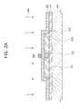
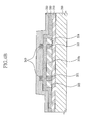
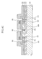
- FIGS. 2A , 2B , 2D , and 2E are cross-sectional views illustrating a process of fabricating a thin film transistor (TFT), according to an exemplary embodiment of the present invention
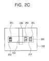
- FIG. 2C is a plan view corresponding to the cross-sectional view of FIG. 2B
- the capping layer 130 and the crystallization-inducing metal layer 140 are removed, and the poly-Si layer (refer to 160 in FIG. 1 D) is patterned, thereby forming a semiconductor layer 210 on the buffer layer 110.
- the poly-Si layer 160 may alternatively be patterned during a subsequent process.
- the gate insulating layer 220 is formed on the semiconductor layer 210 and the buffer layer 110.
- the gate insulating layer 220 may be a silicon oxide layer, a silicon nitride layer, or a multi-layer thereof.
- a metal layer (not shown) for a gate electrode is formed on the gate insulating layer 220.
- the metal layer may be a single layer formed of aluminium (Al), or an Al alloy, such as an aluminium-neodymium (Al-Nd) alloy, or may include multiple layers formed by stacking an Al alloy layer on a chrome (Cr) layer or a molybdenum (Mo) alloy layer.
- the metal layer may be etched using photolithography and etching processes, thereby forming a gate electrode 230.
- a predetermined amount of conductive ions 240 may be implanted into the semiconductor layer 210, using the gate electrode 230 as a mask, thereby forming source and drain regions 211 and 213, and a channel region 212 disposed therebetween.
- the conductive ions may be p-type ions or n-type ions.
- the p-type ions may be ions of one selected from the group consisting of boron (B), aluminium (Al), gallium (Ga), and indium (In).
- the n-type ions may be ions of one selected from the group consisting of phosphorus (P), arsenic (As), and antimony (Sb).
- a photoresist pattern may be formed before the gate electrode 230 is formed, and the conductive ions 240 may be implanted into the semiconductor layer 210, using the photoresist pattern as a mask.
- an interlayer insulating layer 250 is formed on the entire surface of the gate electrode 230.
- the interlayer insulating layer 250 may be a silicon nitride layer, a silicon oxide layer, or a multi-layer thereof.
- regions of the interlayer insulating layer 250 and the gate insulating layer 220 may be etched, thereby forming first holes 261 and a second hole 262.
- the first holes 261 expose regions of the source and drain regions 211 and 213.
- the second hole 262 is spaced apart from the first holes 261.
- the second hole 262 can be formed between the first holes 261.
- the first holes 261 are contact holes for electrically connecting the source and drain regions 211 and 213 with subsequently formed source and drain electrodes.
- the first holes 261 are formed in edges of the semiconductor layer 210, that is, at edges of the source and drain regions 211 and 213.
- the second hole 262 can improve gettering efficiency.
- gettering sites 271 and 272 used for gettering the remaining crystallization-inducing metal from the channel region 212, are formed using the first and second holes 261 and 262, in the regions of the semiconductor layer 210 that are exposed by the first and second holes 261 and 262.
- the first gettering sites 271 are formed using the first holes 261, while the second gettering site 272 is formed using the second hole 262. Since the crystallization-inducing metal remaining in the channel region 212 is gettered into the first and second gettering sites 271 and 272, the concentration of the crystallization-inducing metal is higher in the first and second gettering sites 271 and 272 than in the channel region 212.
- the second gettering site 272 may be disposed in the drain region 213.
- the second gettering site 272 is formed in the source region 211, even if a distance from an interface between the source region 211 and the channel region 212 to the second gettering site 272 is increased, a leakage current does not significantly vary.
- the second gettering site 272 is formed in the drain region 231, as a distance from an interface between the drain region 213 and the channel region 212 to the gettering site 272 is increased, a leakage current gradually increases. Accordingly, since the leakage current is affected by a gettering site disposed in the drain region 213, more than by a gettering site disposed in the source region 211, the second gettering site 272 may be disposed in the drain region 213.
- the second gettering site 272 may be disposed within a distance of about 0.5 to 10 ⁇ m from the interface between the channel region 212 and the drain region 213. When the second gettering site 272 is disposed at more than about 0.5 ⁇ m from the interface between the channel region 212 and the drain region 213, damage to the gate electrode 230 may be prevented during the formation of the second hole 262. When the second gettering site 272 is disposed less than about 10 ⁇ m from the interface between the channel region 212 and the drain region 213, gettering efficiency can be further enhanced. At least two of the second gettering sites 272 may be formed, in order to increase gettering efficiency.
- the formation of the first and second gettering sites 271 and 272 may be performed using: a method of implanting impurities for gettering into the semiconductor layer 210, using the first and second holes 261 and 262; a method of forming a lattice damage region using a plasma; or a method of forming a metallic layer, including a metallic material other than the crystallization-inducing metal. Since the method of forming the metallic layer exhibits a high gettering efficiency, it will now be described.
- a metallic layer 280 is formed on the interlayer insulating layer 250 having the first and second holes 261 and 262.
- the metallic layer 280 can be a metal layer, a metal silicide layer, or a multi-layer thereof.
- the metal layer and the metal silicide layer may be formed using a metal having a lower diffusion coefficient than the crystallization-inducing metal in the semiconductor layer 210, or an alloy of the metal.
- the diffusion coefficient of the metallic layer 280, or components thereof, may be 1/100, or less, of that of the diffusion coefficient of the crystallization-inducing metal in the semiconductor layer 210.
- the metal or metal silicide may be prevented from departing from the gettering sites 271 and 272, which contact the metallic layer 280, and may be prevented from diffusing into other regions of the semiconductor layer 210.
- Nickel (Ni) is widely used as a crystallization-inducing metal in a semiconductor layer. Since Ni has a diffusion coefficient of about 10 -5 cm 2 /s, or less, in a semiconductor layer, the metallic layer 280 may be formed of a metal or metal silicide having a diffusion coefficient that is less than about 1/100 of the diffusion coefficient of Ni, when Ni is used in the semiconductor layer 210. For example, the metallic layer 280, or components thereof, can have a diffusion coefficient between 0 and 10 -7 cm 2 /s.
- the metallic layer 280 may include one selected from the group consisting of Sc, Ti, Zr, Hf, V, Nb, Ta, Cr, Mo, W, Mn, Re, Ru, Os, Co, Rh, Ir, Pt, Y, Ta, La, Ce, Pr, Nd, Dy, Ho, TiN, TaN, an alloy thereof, and a metal silicide thereof.
- the metallic layer 280 may be formed to a thickness of about 30 to 2000 ⁇ .
- the metallic layer 280 is formed to a thickness of less than about 30 ⁇ , the crystallization-inducing metal may not be effectively gettered into the gettering sites 271 and 272.
- the metallic layer 280 is formed to a thickness of more than about 2000 ⁇ , the substrate 200 may be deformed, due to the thermal expansion of the metallic layer 280.
- a thermal oxidation barrier layer 290 may be formed on the metallic layer 280.
- the thermal oxidation barrier layer 290 may prevent the oxidation of the metallic layer 280, and/or the reaction of the metallic layer 280 with a gas, such as nitrogen, during a subsequent annealing process, thereby inhibiting the transformation of the surface of the metallic layer 280.
- the thermal oxidation barrier layer 290 may be a silicon oxide layer or a silicon nitride layer.
- the thermal oxidation barrier layer 290 may be omitted, when the annealing process is carried out in an inert atmosphere.
- the annealing process is performed, in order to remove (getter) the crystallization-inducing metal remaining in the semiconductor layer 210, specifically, from the channel region 212 of the semiconductor layer 210.
- a metal of the metallic layer 280 may diffuse into the semiconductor layer 210 and/or combine with the Si of the semiconductor layer 210, to form a metal silicide.
- a metal silicide of the metallic layer 280 may diffuse into the semiconductor layer 210.
- the metal and/or metal silicide is diffused into the surface of the semiconductor layer 210 to a predetermined depth, in the gettering sites 271 and 272.
- the metal and/or metal silicide may be diffused into the surface of the semiconductor layer 210, to a depth of about 2 to 400 ⁇ , although the depth of the region may be varied, according to an annealing temperature and an annealing time.
- the crystallization-inducing metal diffuses from the channel region 212 of the semiconductor layer 210, into the gettering sites 271 and 272, due to the annealing process, the crystallization-inducing metal precipitates in the gettering sites 271 and 272, and is trapped. This is because the crystallization-inducing metal is thermodynamically more stable in the gettering sites 271 and 272, which contain the metal and/or metal silicide, than in the semiconductor layer 210. Based on the above-described principle, the crystallization-inducing metal can be removed from the channel region 212.
- the annealing process may be performed at a temperature of from about 500 to 993°C, for from 10 seconds to 10 hours.
- the annealing process may be performed at a temperature of lower than 500°C, because the crystallization-inducing metal may not diffuse in the semiconductor layer 210 and may not move to the gettering sites 271 and 272.
- the annealing process may be performed at a temperature of less than about 993°C, because the eutectic point of Ni (the crystallization-inducing metal in the semiconductor layer 210) is 993°C.
- the annealing process When the annealing process is performed for less than 10 seconds, it may be difficult to sufficiently remove the crystallization-inducing metal from the channel region 212. When the annealing process is performed for longer than 10 hours, the substrate 100 may be deformed, and problems may be caused in terms of fabrication costs and yields. When the annealing process is performed at a relatively high temperature, it is possible to remove the crystallization-inducing metal in a relatively short amount of time.
- the thermal oxidation barrier layer 290 and the metallic layer 280 are removed. Then source and drain electrodes 292 and 293 are formed.
- the source and drain electrodes 292 and 293 are connected to the source and drain regions 211 and 213, through the first holes 261.
- the source and drain electrodes 292 and 293 may be formed of one selected from the group consisting of molybdenum (Mo), chrome (Cr), tungsten (W), molybdenumtungsten (MoW), aluminium (Al), aluminium-neodymium (Al-Nd), titanium (Ti), titanium nitride (TiN), copper (Cu), a Mo alloy, an Al alloy, and a Cu alloy.
- a conductive pattern 291 may optionally be formed in the second hole 262.
- the conductive pattern 291 may be a resistance reducer.
- the conductive pattern 291 may be formed by patterning the metallic layer 280. After the source and drain electrodes 292 and 293 and the conductive pattern 291 are formed, a TFT according to the exemplary embodiment of the present invention is completed.
- Table 1 shows a comparison of leakage currents of a TFT having a second gettering site (Example 1), according to the exemplary embodiment of the present invention, and a conventional TFT having no second gettering site (Comparative Example 1).
- a channel region of a semiconductor layer has a width of about 25 ⁇ m and a length of about 20 ⁇ m.
- the distance from an interface of the channel region to a first gettering site is about 50 ⁇ m.
- a distance from the interface of the channel region to the second gettering site is 4 ⁇ m.
- Example 1 the leakage current of Example 1 was markedly reduced, as compared to Comparative Example 1.
- Table 2 shows a comparison of leakage currents of Examples 1-3, according to exemplary embodiments of the present invention, which were TFTs having different numbers of second gettering sites, and a conventional Comparative Example 1, which was a TFT having no second gettering site.
- a channel region of a semiconductor layer had a width of about 25 ⁇ m and a length of about 20 ⁇ m, and the distance from an interface of the channel regions to a first gettering site was about 50 ⁇ m.
- the distance from the interface of the channel region to the second gettering site was 4 ⁇ m.
- Table 3 shows a comparison of leakage currents of TFTs, when a distance from an interface between a channel region and a drain region, to a gettering site formed in the drain region, was 4 ⁇ m, 10 ⁇ m, 30 ⁇ m, and 50 ⁇ m, respectively.
- the channel regions had a width of about 25 ⁇ m and a length of about 20 ⁇ m, and the distance from the interface between the channel region and a source region to a gettering site formed in the source region was about 4 ⁇ m.
- Table 4 shows a comparison of leakage currents of TFTs, when a distance from an interface between a channel region and a source region to a gettering site formed in the source region was 4 ⁇ m, 10 ⁇ m, 30 ⁇ m, and 50 ⁇ m, respectively.
- the channel region had a width of about 25 ⁇ m and a length of about 20 ⁇ m, the distance from an interface between the channel region and a drain region to a gettering site formed in the drain region was about 4 ⁇ m.
- Table 5 shows a comparison of leakage currents of TFTs, when a distance from an interface of a channel region to each of gettering sites formed in source and drain regions was 4 ⁇ m, 10 ⁇ m, 30 ⁇ m, and 50 ⁇ m, respectively. In all the TFTs, the channel region had a width of about 25 ⁇ m and a length of about 20 ⁇ m.
- an additional second gettering site may be formed within a distance of about 10 ⁇ m from the interface of the channel region.
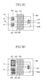
- FIGS. 3A through 3D are plan views illustrating a process of fabricating a dual-gate TFT, according to another exemplary embodiment of the present invention
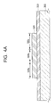
- FIGS. 4A through 4D are cross-sectional views taken along lines 1A-1A' of FIGS. 3A through 3D , respectively.
- the process of fabricating the dual-gate TFT will now be described, with reference to the method shown in FIGS. 2A through 2E , except for particulars mentioned below.
- a poly-Si layer (refer to 160 in FIG. 1D ), obtained using an SGS crystallization method as described with reference to FIGS. 1A and 1D , is patterned, thereby forming a semiconductor layer 320 on a substrate 300 having a buffer layer 310.
- the semiconductor layer 320 includes body units 320a and 320c, and a connection unit 320b connecting the body units 320a and 320c.
- the body units 320a and 320c are sides where source regions, drain regions, and/or channel regions are formed. That is, the semiconductor layer 320 may have a " "-shaped structure.
- FIG. 3A illustrates the semiconductor layer 320 with the " "-shaped structure, the present invention is not limited thereto.
- the semiconductor layer 320 may have a " "-shaped structure, a " “-shaped structure, or a combination thereof.
- a gate insulating layer 330 is formed on the semiconductor layer 320.
- a gate electrode 340 is formed on the gate insulating layer 330.
- the gate electrode 340 may intersect the body units 320a and 320c of the semiconductor layer 320.
- a portion 321 of the first body unit 320a that overlaps the gate electrode 340 may be referred to as a first gate, and a portion 322 of the second body unit 320c that overlaps the gate electrode 340, may be referred to as a second gate.
- a dual gate structure is obtained.
- the semiconductor layer 320 has a plurality of body units with a zigzag structure, instead of the " "-shaped structure, portions of the body units, which overlap the gate electrode 340, can be referred to as gates. Therefore, a multi-gate TFT may be fabricated.
- a predetermined amount of conductive ions may be implanted into the semiconductor layer 320, using the gate electrode 340 as a mask.
- the portions 321 and 322 of the semiconductor layer 320, which overlap the gate electrode 340, can be referred to as channel regions.
- Outer regions of the body units 320a and 320c, which are not connected to the connection unit 320b, can be referred to as source and drain regions 323 and 324.
- an interlayer insulating layer 350 is formed on the entire surface of the gate insulating layer 330 and the gate electrode 340.
- the interlayer insulating layer 350 and the gate insulating layer 330 are etched, thereby forming first holes 361 and a second hole 362.
- the first holes 361 expose portions of the source and drain regions 323 and 324 of the semiconductor layer 320.
- the second hole 362 is spaced apart from the first holes 361 and partially exposes a region between the channel regions 321 and 322.
- the first holes 361 are contact holes for electrically connecting the source and drain regions 323 and 324 with subsequently formed source and drain electrodes.
- the second hole 362 is formed to increase gettering efficiency.
- first gettering sites 371 and a second gettering site 372, for gettering the remaining crystallization-inducing metal from the channel regions 321 and 322, are formed in predetermined regions of the semiconductor layer 320 that are exposed by the first and second holes 361 and 362.
- the first gettering sites 371 are formed using the first holes 361, and the second gettering site 372 is formed using the second hole 362.
- the second gettering site 372 may be disposed closer to the drain region 324 than to the source region 323.
- the second gettering site 372 is disposed close to the source region 323, even if a distance from interfaces of the channel region 321 and 322 to the second gettering site 372 is increased, a leakage current does not significantly vary.
- the second gettering site 372 is formed close to the drain region 324, as a distance from the interfaces of the channel regions 321 and 322 to the second gettering site 372 is increased, a leakage current gradually increases. Accordingly, since the leakage current is affected by a gettering site disposed close to the drain region 324, the second gettering site 372 may be disposed closer to the drain region 324 than to the source region 323.
- the second gettering site 372 may be disposed from about 0.5 to 10 ⁇ m from the interfaces of the channel regions 321 and 322. When the second gettering site 372 is more than about 0.5 ⁇ m from the interfaces of the channel regions 321 and 322, damage to the gate electrode 340 may be prevented, during the formation of the second hole 362. When the second gettering site 372 is disposed at less than about 10 ⁇ m from the interfaces of the channel regions 321 and 322, the gettering efficiency can be enhanced. At least two second gettering sites 372 may be formed, in order to further enhance the gettering efficiency.
- the first and second gettering sites 371 and 372 may be formed using: a method of implanting impurities into the semiconductor layer 320, using the first and second holes 361 and 362; a method of using plasma to form a lattice damage region; or a method of forming a region containing a metal other than the crystallization-inducing metal or a silicide of the metal. Thereafter, an annealing process may be performed, to getter the crystallization-inducing metal from the channel regions 321 and 322, into the first and second gettering sites 371 and 372.
- source and drain electrodes 381 and 382 are connected to the source and drain regions 323 and 324, through the first holes 361.
- a conductive pattern 383 may be formed, which is connected to the semiconductor layer 320, through the second hole 362.
- the conductive pattern 383 may be referred to as a resistance reducer.
- Table 6 shows a comparison of leakage currents of a dual-gate TFT having one second gettering site (Example 4), according to the present exemplary embodiment, and a conventional dual-gate TFT having no second gettering site (Comparative Example 4).
- a channel region of a semiconductor layer had a width of about 7 ⁇ m and a length of about 14 ⁇ m.
- the distance from an interface of the channel region to the second gettering site was about 4 ⁇ m.
- Example 4 (Dual-gate TFT with one second gettering gate) 2.89*10 -13
- Example 4 had a smaller leakage current than Comparative Example 2.
- FIG. 5 is a cross-sectional view of an organic light emitting diode (OLED) display device including a TFT, according to an exemplary embodiment of the present invention.
- OLED organic light emitting diode
- an insulating layer 510 is formed on the entire surface of a substrate 100, having the TFT fabricated according to the method described with reference to FIGS. 2A through 2E .
- the insulating layer 510 may be an inorganic layer, an organic layer, or a multi-layer layer thereof.
- the inorganic layer may be formed of one selected from the group consisting of silicon oxide, silicon nitride, or silicon on glass (SOG).
- the organic layer may be formed of one selected from the group consisting of polyimide, a benzocyclobutene series resin, and acrylate.
- the insulating layer 510 may be etched, thereby forming a hole exposing the source and drain electrodes 292 and 293.
- a first electrode 520 is connected to one of the source and drain electrodes 292 and 293, through the hole.
- the first electrode 520 may be an anode or a cathode.
- the first electrode 520 may be formed of a transparent conductive material selected from the group consisting of indium tin oxide (ITO), indium zinc oxide (IZO), and indium tin zinc oxide (ITZO).
- ITO indium tin oxide
- IZO indium zinc oxide
- ITZO indium tin zinc oxide
- the first electrode 520 is a cathode, it may be formed of one selected from the group consisting of Mg, Ca, Al, Ag, Ba, and an alloy thereof.
- a pixel defining layer 530 is formed on the first electrode 520.
- the pixel defining layer 530 has an opening exposing the surface of the first electrode 520.
- An organic layer 540 having an emission layer (EML) is formed on the exposed surface of the first electrode 520.
- the organic layer 540 may further include at least one selected from the group consisting of a hole injection layer (HIL), a hole transport layer (HTL), a hole blocking layer (HBL), an electron blocking layer (EBL), an electron injection layer (EIL), and an electron transport layer (ETL).
- HIL hole injection layer
- HTL hole transport layer
- HBL hole blocking layer
- EBL electron blocking layer
- EIL electron injection layer
- ETL electron transport layer
- At least one second gettering site is formed, which is spaced apart from the first gettering site.
- a crystallization-inducing metal is removed from a channel region of the semiconductor layer, using the first and second gettering sites.
- the present invention provides a TFT including a semiconductor layer formed using a poly-Si layer, which is crystallized using a crystallization-inducing metal, a method of fabricating the TFT, and an OLED display device having the TFT.
- the crystallization-inducing metal can be effectively gettered from a channel region of the semiconductor layer, thereby improving leakage current characteristics.
Abstract
Description
- Aspects of the present invention relate to a thin film transistor (TFT), a method of fabricating the same, and an organic light emitting diode (OLED) display device including the TFT.
- In general, a polycrystalline silicon (poly-Si) layer is widely used as a semiconductor layer for a thin film transistor (TFT), because a poly-Si layer has a high field-effect mobility and may be applied to a high-speed operating circuit, or to a complementary-metal-oxide-semiconductor (CMOS) circuit. A TFT using a poly-Si layer is typically used as an active device of an active-matrix liquid crystal display (AMLCD), or as a switching device or a driving device of an active-matrix organic light emitting diode display device(AMOLED).
- The crystallization of an amorphous silicon (a-Si) semiconductor layer may be performed using a solid phase crystallization (SPC) process, an excimer laser annealing (ELA) process, a metal induced crystallization (MIC) process, or a metal induced lateral crystallization (MILC) process. Specifically, the SPC process includes annealing an a-Si layer for several hours, to several tens of hours, at temperatures below 700 °C, which is the temperature at which a glass substrate, used in a TFT for a display device, is deformed. The ELA process includes heating an a-Si layer to a high temperature, in a short amount of time, by irradiating the a-Si layer with an excimer laser. The MIC process includes bringing a metal, such as nickel (Ni), palladium (Pd), gold (Au), or aluminium (Al), into contact with an a-Si layer, or injecting the metal into the a-Si layer, to phase-change the a-Si layer into a poly-Si layer. Also, the MILC process includes sequentially inducing the crystallization of an a-Si layer, while laterally diffusing a silicide, which is obtained by a reaction between a metal and silicon.
- However, since the SPC process involves annealing a substrate at a high temperature, for a long period of time, the substrate can be easily damaged. Also, the ELA process requires an expensive laser apparatus and may damage the crystallized surface, thereby degrading an interface between a semiconductor layer and a gate insulating layer.
- A vast amount of research has been conducted on methods of crystallizing an a-Si layer using a metal, because such methods allow an a-Si layer to be crystallized at a lower temperature, for a shorter amount of time, than the SPC method. Typical methods of crystallizing an a-Si layer using a metal include an MIC method, an MILC method, and a super grain silicon (SGS) crystallization method. In these methods, however, the device characteristics of a TFT may be degraded, due to contamination caused by a crystallization-inducing metal. Accordingly, after an a-Si layer is crystallized using the crystallization-inducing metal, a gettering process is performed to remove the remaining crystallization-inducing metal.
- A gettering site is formed in a semiconductor layer, in order to perform the gettering process. Conventionally, the formation of the gettering site involves implanting a gettering material into a region of the semiconductor layer, using a contact hole, which is used to connect source and drain regions of the semiconductor layer with source and drain electrodes. However, when a distance between a channel region and the contact hole is increased, a gettering process that uses only the contact hole gettering site is not very effective.
- Aspects of the present invention provide a thin film transistor (TFT) including a semiconductor layer formed of a polycrystalline silicon (poly-Si) layer, which is crystallized using a crystallization-inducing metal. The crystallization-inducing metal can be effectively gettered from a channel region of the semiconductor layer, so as to improve the electrical characteristics thereof, such as leakage current characteristics. A method of fabricating the TFT, and an organic light emitting diode (OLED) display device having the TFT, are also provided.
- According to an aspect of the present invention, a TFT includes: a substrate; a semiconductor layer disposed on the substrate, including source, drain, and channel regions; a gate insulating layer disposed on the semiconductor layer; a gate electrode disposed on the gate insulating layer; an interlayer insulating layer disposed on the gate electrode; and source and drain electrodes disposed on the interlayer insulating layer and electrically connected to the source and drain regions of the semiconductor layer. The semiconductor layer is formed of a polycrystalline silicon (poly-Si) layer that is crystallized using a crystallization-inducing metal. The semiconductor layer includes first gettering sites disposed on opposing edges of the semiconductor layer, and at least one second gettering site spaced apart from the first gettering sites.
- Preferably the second gettering site is disposed in the drain region of the semiconductor layer. Preferably the second gettering site is disposed within about 0.5 to 10 µm of an interface between the channel region and the drain region. Preferably the semiconductor layer includes at least two of the second gettering sites. Preferably the gate insulating layer and the interlayer insulating layer have: first holes exposing the first gettering sites; and a second hole exposing the second gettering site. Preferably the source and drain electrodes are respectively connected to the source and drain regions of the semiconductor layer, through the first holes. Preferably the first and second gettering sites each include a lattice damage region, or a gettering impurity. Preferably each of the first and second gettering sites comprises a metallic material having a lower diffusion coefficient than the crystallization-inducing metal, which is diffused into the surface of the semiconductor layer, to a predetermined depth. Preferably the diffusion coefficient of the metallic material is less than about 1/100 of the diffusion coefficient of the crystallization-inducing metal. Preferably the metallic material comprises one selected from the group consisting of Sc, Ti, Zr, Hf, V, Nb, Ta, Cr, Mo, W, Mn, Re, Ru, Os, Co, Rh, Ir, Pt, Y, La, Ce, Pr, Nd, Dy, Ho, an alloy thereof, and a silicide thereof. Preferably the semiconductor layer comprises: a plurality of the source, drain, and channel regions; and a plurality of the second gettering sites disposed between the channel regions. Preferably the semiconductor layer comprises body units intersecting the gate electrode; and at least one connection portion connecting adjacent first edges of the body units; and the first gettering sites are disposed on second edges of the body units, which are not connected by the connection unit. Preferably the second gettering sites are disposed closer to the drain regions than to the source regions. Preferably the second gettering sites are each disposed within about 0.5 to 10 µm of an interface between one of the channel regions and the one of drain regions.
- According to another aspect of the present invention, a method of fabricating a TFT includes: providing a substrate; forming a semiconductor layer, including source, drain, and channel regions, on the substrate, by patterning a poly-Si layer that is crystallized using a crystallization-inducing metal; forming a gate insulating layer on the semiconductor layer; forming a gate electrode on the gate insulating layer; forming an interlayer insulating layer on the gate electrode; forming first holes and at least one second hole, by patterning the interlayer insulating layer and the gate insulating layer; forming gettering sites in regions of the semiconductor layer, which are exposed by the first and second holes; gettering the crystallization-inducing metal remaining in the channel region of the semiconductor layer, using the gettering sites; and forming source and drain electrodes that are electrically connected to the source and drain regions of the semiconductor layer, through the first holes. The first holes expose regions of the semiconductor layer, and the at least one second hole is spaced apart from the first holes.
- Preferably the second hole is disposed on the drain region of the semiconductor layer. Preferably the second hole is formed within about 0.5 to 10 µm of an interface between the channel region and the drain region. Preferably the step of the forming of the gettering sites comprises implanting gettering impurities into the exposed regions of the semiconductor layer, or using a plasma to form lattice damage regions in the exposed regions of the semiconductor layer; and the gettering of the crystallization-inducing metal comprises performing an annealing process. Preferably the forming of the gettering sites comprises forming a metallic layer on the interlayer insulating layer, the metallic layer having a lower diffusion coefficient than the crystallization-inducing metal; and the gettering of the crystallization-inducing metal comprises performing an annealing process. Preferably the metallic layer comprises, one or more layers formed of one selected from the group consisting of Sc, Ti, Zr, Hf, V, Nb, Ta, Cr, Mo, W, Mn, Re, Ru, Os, Co, Rh, Ir, Pt, Y, La, Ce, Pr, Nd, Dy, Ho, an alloy thereof, and a metal silicide thereof. Preferably the method further comprises forming a thermal oxidation barrier layer on the metallic layer. Preferably the poly-Si layer is crystallized using a super grain silicon (SGS) crystallization process.
- According to yet another aspect of the present invention, an OLED display device includes: a substrate; a semiconductor layer disposed on the substrate and including source, drain, and channel regions; a gate insulating layer disposed on the semiconductor layer; a gate electrode disposed on the gate insulating layer; an interlayer insulating layer disposed on the gate electrode; source and drain electrodes disposed on the interlayer insulating layer and electrically connected to the source and drain regions of the semiconductor layer, respectively; a first electrode electrically connected to one of the source and drain electrodes; an organic layer disposed on the first electrode and including an emission layer (EML); and a second electrode disposed on the organic layer. The semiconductor layer is formed of a poly-Si layer that is crystallized using a crystallization-inducing metal. The semiconductor layer includes first gettering sites disposed on opposing edges of the semiconductor layer, and a at least one second gettering site that is spaced apart from the first gettering sites.
- Preferably the second gettering site is disposed in the drain region of the semiconductor layer. Preferably the second gettering site is disposed within 0.5 to 10 µm of an interface between the channel region and the drain region. Preferably the second gettering site is disposed between the first gettering sites. Preferably the second hole is disposed between the first holes. Preferably the second gettering site is disposed between the first gettering sites.
- Additional aspects and/or advantages of the invention will be set forth in part in the description which follows and, in part, will be obvious from the description, or may be learned by practice of the invention.
- These and/or other aspects and advantages of the invention will become apparent and more readily appreciated from the following description of the embodiments, taken in conjunction with the accompanying drawings of which:
-
FIGS. 1A through 1D are cross-sectional views illustrating a crystallization process, according to an exemplary embodiment of the present invention; -
FIGS. 2A ,2B ,2D , and2E are cross-sectional views illustrating a process of fabricating a thin film transistor (TFT), according to an exemplary embodiment of the present invention; -
FIG. 2C is a plan view corresponding to the cross-sectional view ofFIG. 2B ; -
FIGS. 3A through 3D are plan views illustrating a process of fabricating a dual-gate TFT, according to another exemplary embodiment of the present invention; -
FIGS. 4A through 4D are cross-sectional views illustrating the process of fabricating the dual-gate TFT corresponding toFIGS. 3A through 3D ; and -
FIG. 5 is a cross-sectional view of an organic light emitting diode (OLED) display device, according to an exemplary embodiment of the present invention. - Reference will now be made in detail to the exemplary embodiments of the present invention, examples of which are illustrated in the accompanying drawings, wherein like reference numerals refer to the like elements throughout. The exemplary embodiments are described below, in order to explain the aspects of the present invention, by referring to the figures.
- As referred to herein, when a first element is said to be disposed or formed "on", or "adjacent to", a second element, the first element can directly contact the second element, or can be separated from the second element by one or more other elements located therebetween. In contrast, when an element is referred to as being disposed or formed "directly on" another element, there are no intervening elements present. As used herein, the term "and/or" includes any and all combinations of one or more of the associated listed items.
-
FIGS. 1A through 1D are cross-sectional views illustrating a crystallization process, according to an exemplary embodiment of the present invention. Referring toFIG. 1A , abuffer layer 110 is formed on asubstrate 100, such as a glass substrate, or a plastic substrate. Thebuffer layer 110 may be formed using a chemical vapor deposition (CVD) technique, or a physical vapor deposition (PVD) technique. Thebuffer layer 110 may be formed of one or more insulating layers, such as a silicon oxide layer or a silicon nitride layer. Thebuffer layer 110 may prevent the diffusion of moisture or impurities generated in thesubstrate 100, or may control the transmission rate of heat during a crystallization process, thereby facilitating the crystallization of an amorphous silicon (a-Si) layer. - Thereafter, an
a-Si layer 120 is formed on thebuffer layer 110. Thea-Si layer 120 may be formed using a CVD or a PVD technique. Also, a dehydrogenation process may be performed during or after the formation of thea-Si layer 120, thereby lowering the concentration of hydrogen in thea-Si layer 120. - The
a-Si layer 120 is then crystallized into a poly-Si layer. Thea-Si layer 120 may be crystallized into the poly-Si layer, by a crystallization method using a crystallization-inducing metal, such as a metal-induced crystallization (MIC) method, a metal-induced lateral crystallization (MILC) method, or a super grain silicon (SGS) crystallization method. - In the SGS crystallization method, a crystallization-inducing metal is diffused into an a-Si layer, at a low concentration, such that the crystal grain size thereof ranges from several µm to several hundred µm. For example, the SGS crystallization method may include: forming a capping layer, for controlling the diffusion of a crystallization-inducing metal, on the a-Si layer; forming a crystallization-inducing metal layer on the capping layer; and annealing the crystallization-inducing metal layer, to diffuse a crystallization-inducing metal into the a-Si layer, and thereby crystallize the a-Si layer into a poly-Si layer. Alternatively, the concentration of a crystallization-inducing metal may be lowered, by forming a crystallization-inducing metal layer at a low concentration, without forming a capping layer.
- According to the SGS crystallization method using a capping layer, the concentration of a crystallization-inducing metal is controlled more effectively than in the MIC or MILC methods. Thus, the SGS crystallization method will now be described.
-
FIG. 1B is a cross-sectional view illustrating a process of forming a capping layer and a crystallization-inducing metal layer on the a-Si layer. Referring toFIG. 1B , acapping layer 130 is formed on thea-Si layer 120. Thecapping layer 130 may be a silicon nitride layer, into which a crystallization-inducing metal may diffuse during a subsequent annealing process, or may be a double layer of a silicon nitride layer and a silicon oxide layer. - The
capping layer 130 may be formed using a CVD technique or a PVD technique. Thecapping layer 130 may be formed to a thickness of about 1 to 2000Å. When thecapping layer 130 is formed to a thickness of less than about 1Å, thecapping layer 130 may not properly control the amount of crystallization-inducing metal that diffuses into thea-Si layer 120. When thecapping layer 130 is formed to a thickness of more than about 2000Å, only a small amount of crystallization-inducing metal diffuses into thea-Si layer 120, thereby possibly resulting in an incomplete crystallization of thea-Si layer 120. - Thereafter, a crystallization-inducing metal is deposited on the
capping layer 130, thereby forming a crystallization-inducingmetal layer 140. The crystallization-inducing metal may include one selected from the group consisting of Ni, Pd, Ag, Au, Al, Sn, Sb, Cu, Tr, and Cd. If the crystallization-inducing metal is Ni, the crystallization-inducingmetal layer 140 may be formed with a surface density of about 1011 to 1015 atoms/cm2, on thecapping layer 130. - When the crystallization-inducing
metal layer 140 is formed with a surface density lower than about 1011 atoms/cm2, only a small number of seeds may be formed, thereby hindering the crystallization of thea-Si layer 120 into a poly-Si layer. When the crystallization-inducingmetal layer 140 is formed with a surface density of more than about 1015 atoms/cm2, the amount of crystallization-inducing metal diffusing into thea-Si layer 120 may be increased, thereby reducing the crystal grain size of the poly-Si layer. Also, the amount of the remaining crystallization-inducing metal may be increased, so that the characteristics of a semiconductor layer, formed by patterning the poly-Si layer, may be degraded. -
FIG. 1C is a cross-sectional view illustrating a process of annealing thesubstrate 100, to diffuse the crystallization-inducing metal through thecapping layer 130 and into thea-Si layer 120. Referring toFIG. 1C , thesubstrate 100, including thebuffer layer 110, thea-Si layer 120, thecapping layer 130, and the crystallization-inducingmetal layer 140, is annealed (refer to 150), so that part of the crystallization-inducing metal of the crystallization-inducingmetal layer 140 may diffuse into the surface of thea-Si layer 120. Specifically, during theannealing process 150, only a small amount of crystallization-inducingmetal 140b is diffused into the surface of thea-Si layer 120, while a large amount of crystallization-inducingmetal 140a neither reaches thea-Si layer 120, nor passes through thecapping layer 130. - Thus, the amount of crystallization-inducing metal diffused into the surface of the
a-Si layer 120 may depend on the diffusion barrier characteristics of thecapping layer 120, which are closely related to the thickness and/or density of thecapping layer 130. In other words, as the thickness and/or density of thecapping layer 130 increases, the diffused amount of crystallization-inducing metal decreases, and the crystal grain size increases. Conversely, as the thickness and/or density of thecapping layer 130 decreases, the diffused amount of crystallization-inducing metal increases, and the crystal grain size decreases. - In this case, the
annealing process 150 may be performed at a temperature of about 200 to 900°C, for from several seconds to several hours. When theannealing process 150 is performed under the above-described time and temperature conditions, the deformation of thesubstrate 100, due to overheating, may be prevented, and desired fabrication costs and yields may be achieved. Theannealing process 150 may be performed using any one of a furnace process, a rapid thermal annealing (RTA) process, an ultraviolet (UV) process, and a laser process. -
FIG. 1D is a cross-sectional view illustrating a process of crystallizing thea-Si layer 140 into a poly-Si layer 160, using the diffused crystallization-inducingmetal 140b. Referring toFIG. 1D , due to the crystallization-inducingmetal 140b that passes through thecapping layer 130 and diffuses into the surface of thea-Si layer 120, thea-Si layer 120 is crystallized into the poly-Si layer 160. That is, the diffused crystallization-inducingmetal 140b combines with the Si of thea-Si layer 120, to form a metal silicide. Thus, the metal silicide forms crystallization nuclei (i.e., seeds), thereby crystallizing thea-Si layer 120 into the poly-Si layer 160. -
FIG. 1D illustrates that the annealing process is performed on the structure having thecapping layer 130 and the crystallization-inducingmetal layer 140. However, after the crystallization-inducing metal is diffused into the surface of thea-Si layer 120, thecapping layer 130 and the crystallization-inducingmetal layer 140 may be removed, before the annealing process is performed. -
FIGS. 2A ,2B ,2D , and2E are cross-sectional views illustrating a process of fabricating a thin film transistor (TFT), according to an exemplary embodiment of the present invention, andFIG. 2C is a plan view corresponding to the cross-sectional view ofFIG. 2B . Referring toFIG. 2A , thecapping layer 130 and the crystallization-inducingmetal layer 140 are removed, and the poly-Si layer (refer to 160 inFIG. 1 D) is patterned, thereby forming asemiconductor layer 210 on thebuffer layer 110. The poly-Si layer 160 may alternatively be patterned during a subsequent process. - Thereafter, a
gate insulating layer 220 is formed on thesemiconductor layer 210 and thebuffer layer 110. Thegate insulating layer 220 may be a silicon oxide layer, a silicon nitride layer, or a multi-layer thereof. - A metal layer (not shown) for a gate electrode is formed on the
gate insulating layer 220. The metal layer may be a single layer formed of aluminium (Al), or an Al alloy, such as an aluminium-neodymium (Al-Nd) alloy, or may include multiple layers formed by stacking an Al alloy layer on a chrome (Cr) layer or a molybdenum (Mo) alloy layer. The metal layer may be etched using photolithography and etching processes, thereby forming agate electrode 230. - Thereafter, a predetermined amount of
conductive ions 240 may be implanted into thesemiconductor layer 210, using thegate electrode 230 as a mask, thereby forming source and drainregions channel region 212 disposed therebetween. The conductive ions may be p-type ions or n-type ions. The p-type ions may be ions of one selected from the group consisting of boron (B), aluminium (Al), gallium (Ga), and indium (In). The n-type ions may be ions of one selected from the group consisting of phosphorus (P), arsenic (As), and antimony (Sb). Alternatively a photoresist pattern may be formed before thegate electrode 230 is formed, and theconductive ions 240 may be implanted into thesemiconductor layer 210, using the photoresist pattern as a mask. - Referring to
FIGS. 2B and2C , aninterlayer insulating layer 250 is formed on the entire surface of thegate electrode 230. The interlayer insulatinglayer 250 may be a silicon nitride layer, a silicon oxide layer, or a multi-layer thereof. - Subsequently, regions of the interlayer insulating
layer 250 and thegate insulating layer 220 may be etched, thereby formingfirst holes 261 and asecond hole 262. Thefirst holes 261 expose regions of the source and drainregions second hole 262 is spaced apart from thefirst holes 261. For example, thesecond hole 262 can be formed between thefirst holes 261. Thefirst holes 261 are contact holes for electrically connecting the source and drainregions first holes 261 are formed in edges of thesemiconductor layer 210, that is, at edges of the source and drainregions second hole 262 can improve gettering efficiency. - Thereafter,
gettering sites channel region 212, are formed using the first andsecond holes semiconductor layer 210 that are exposed by the first andsecond holes first gettering sites 271 are formed using thefirst holes 261, while thesecond gettering site 272 is formed using thesecond hole 262. Since the crystallization-inducing metal remaining in thechannel region 212 is gettered into the first andsecond gettering sites second gettering sites channel region 212. - The
second gettering site 272 may be disposed in thedrain region 213. When thesecond gettering site 272 is formed in thesource region 211, even if a distance from an interface between thesource region 211 and thechannel region 212 to thesecond gettering site 272 is increased, a leakage current does not significantly vary. However, when thesecond gettering site 272 is formed in the drain region 231, as a distance from an interface between thedrain region 213 and thechannel region 212 to thegettering site 272 is increased, a leakage current gradually increases. Accordingly, since the leakage current is affected by a gettering site disposed in thedrain region 213, more than by a gettering site disposed in thesource region 211, thesecond gettering site 272 may be disposed in thedrain region 213. - The
second gettering site 272 may be disposed within a distance of about 0.5 to 10 µm from the interface between thechannel region 212 and thedrain region 213. When thesecond gettering site 272 is disposed at more than about 0.5 µm from the interface between thechannel region 212 and thedrain region 213, damage to thegate electrode 230 may be prevented during the formation of thesecond hole 262. When thesecond gettering site 272 is disposed less than about 10 µm from the interface between thechannel region 212 and thedrain region 213, gettering efficiency can be further enhanced. At least two of thesecond gettering sites 272 may be formed, in order to increase gettering efficiency. - The formation of the first and
second gettering sites semiconductor layer 210, using the first andsecond holes - Referring to
FIG. 2D , ametallic layer 280 is formed on theinterlayer insulating layer 250 having the first andsecond holes metallic layer 280 can be a metal layer, a metal silicide layer, or a multi-layer thereof. The metal layer and the metal silicide layer may be formed using a metal having a lower diffusion coefficient than the crystallization-inducing metal in thesemiconductor layer 210, or an alloy of the metal. The diffusion coefficient of themetallic layer 280, or components thereof, may be 1/100, or less, of that of the diffusion coefficient of the crystallization-inducing metal in thesemiconductor layer 210. When the diffusion coefficient of themetallic layer 280 is less than about 1/100 of that of the crystallization-inducing metal, the metal or metal silicide may be prevented from departing from thegettering sites metallic layer 280, and may be prevented from diffusing into other regions of thesemiconductor layer 210. - Nickel (Ni) is widely used as a crystallization-inducing metal in a semiconductor layer. Since Ni has a diffusion coefficient of about 10-5 cm2/s, or less, in a semiconductor layer, the
metallic layer 280 may be formed of a metal or metal silicide having a diffusion coefficient that is less than about 1/100 of the diffusion coefficient of Ni, when Ni is used in thesemiconductor layer 210. For example, themetallic layer 280, or components thereof, can have a diffusion coefficient between 0 and 10-7 cm2/s. Themetallic layer 280 may include one selected from the group consisting of Sc, Ti, Zr, Hf, V, Nb, Ta, Cr, Mo, W, Mn, Re, Ru, Os, Co, Rh, Ir, Pt, Y, Ta, La, Ce, Pr, Nd, Dy, Ho, TiN, TaN, an alloy thereof, and a metal silicide thereof. - Also, the
metallic layer 280 may be formed to a thickness of about 30 to 2000Å. When themetallic layer 280 is formed to a thickness of less than about 30Å, the crystallization-inducing metal may not be effectively gettered into thegettering sites metallic layer 280 is formed to a thickness of more than about 2000Å, the substrate 200 may be deformed, due to the thermal expansion of themetallic layer 280. - Thereafter, a thermal
oxidation barrier layer 290 may be formed on themetallic layer 280. The thermaloxidation barrier layer 290 may prevent the oxidation of themetallic layer 280, and/or the reaction of themetallic layer 280 with a gas, such as nitrogen, during a subsequent annealing process, thereby inhibiting the transformation of the surface of themetallic layer 280. The thermaloxidation barrier layer 290 may be a silicon oxide layer or a silicon nitride layer. The thermaloxidation barrier layer 290 may be omitted, when the annealing process is carried out in an inert atmosphere. - The annealing process is performed, in order to remove (getter) the crystallization-inducing metal remaining in the
semiconductor layer 210, specifically, from thechannel region 212 of thesemiconductor layer 210. Thus, a metal of themetallic layer 280 may diffuse into thesemiconductor layer 210 and/or combine with the Si of thesemiconductor layer 210, to form a metal silicide. Alternatively, a metal silicide of themetallic layer 280 may diffuse into thesemiconductor layer 210. As a result, the metal and/or metal silicide is diffused into the surface of thesemiconductor layer 210 to a predetermined depth, in thegettering sites semiconductor layer 210, to a depth of about 2 to 400Å, although the depth of the region may be varied, according to an annealing temperature and an annealing time. - When the crystallization-inducing metal diffuses from the
channel region 212 of thesemiconductor layer 210, into thegettering sites gettering sites gettering sites semiconductor layer 210. Based on the above-described principle, the crystallization-inducing metal can be removed from thechannel region 212. - The annealing process may be performed at a temperature of from about 500 to 993°C, for from 10 seconds to 10 hours. When the annealing process is performed at a temperature of lower than 500°C, the crystallization-inducing metal may not diffuse in the
semiconductor layer 210 and may not move to thegettering sites - When the annealing process is performed for less than 10 seconds, it may be difficult to sufficiently remove the crystallization-inducing metal from the
channel region 212. When the annealing process is performed for longer than 10 hours, thesubstrate 100 may be deformed, and problems may be caused in terms of fabrication costs and yields. When the annealing process is performed at a relatively high temperature, it is possible to remove the crystallization-inducing metal in a relatively short amount of time. - Referring to
FIG. 2E , the thermaloxidation barrier layer 290 and themetallic layer 280 are removed. Then source and drainelectrodes electrodes regions first holes 261. The source and drainelectrodes - A
conductive pattern 291 may optionally be formed in thesecond hole 262. Theconductive pattern 291 may be a resistance reducer. Theconductive pattern 291 may be formed by patterning themetallic layer 280. After the source and drainelectrodes conductive pattern 291 are formed, a TFT according to the exemplary embodiment of the present invention is completed. - Table 1 shows a comparison of leakage currents of a TFT having a second gettering site (Example 1), according to the exemplary embodiment of the present invention, and a conventional TFT having no second gettering site (Comparative Example 1). In both of the TFTs, a channel region of a semiconductor layer has a width of about 25 µm and a length of about 20 µm. In addition, the distance from an interface of the channel region to a first gettering site is about 50 µm. In Example 1, a distance from the interface of the channel region to the second gettering site is 4 µm.
[Table 1] Leakage current (A/µm) Example 1 8.92*10-13 Comparative Example 1 3.15*10-12 - Referring to Table 1, the leakage current of Example 1 was markedly reduced, as compared to Comparative Example 1.
- Table 2 shows a comparison of leakage currents of Examples 1-3, according to exemplary embodiments of the present invention, which were TFTs having different numbers of second gettering sites, and a conventional Comparative Example 1, which was a TFT having no second gettering site. In all the TFTs, a channel region of a semiconductor layer had a width of about 25 µm and a length of about 20 µm, and the distance from an interface of the channel regions to a first gettering site was about 50 µm. In Examples 1-3, the distance from the interface of the channel region to the second gettering site was 4 µm.
[Table 2] Leakage current (A/µm) Comparative Example 1 (TFT with no second gettering site) 3.15*10-12 Example 1 (TFT with 1 second gettering site) 8.92*10-13 Example 2 (TFT with 2 second gettering sites) 5.44*10-13 Example 3 (TFT with 3 second gettering sites) 5.07*10-13 - Referring to Table 2, it can be confirmed that in Examples 2 and 3, which included at least two second gettering sites, the leakage current was reduced, as compared to Comparative Example 1, which had only one second gettering site.
- Table 3 shows a comparison of leakage currents of TFTs, when a distance from an interface between a channel region and a drain region, to a gettering site formed in the drain region, was 4 µm, 10 µm, 30 µm, and 50 µm, respectively. In all the TFTs, the channel regions had a width of about 25 µm and a length of about 20 µm, and the distance from the interface between the channel region and a source region to a gettering site formed in the source region was about 4 µm.
- Table 4 shows a comparison of leakage currents of TFTs, when a distance from an interface between a channel region and a source region to a gettering site formed in the source region was 4 µm, 10 µm, 30 µm, and 50 µm, respectively. In all the TFTs, the channel region had a width of about 25 µm and a length of about 20 µm, the distance from an interface between the channel region and a drain region to a gettering site formed in the drain region was about 4 µm.
[Table 3] Distance from interface between channel region and drain region to gettering site formed in drain region Leakage current (A/µm) 4 µm 5.47*10-13 10 µm 7.60*10-13 30 µm 2.33*10-12 50 µm 3.06*10-12 [Table 4] Distance from interface between channel region and source region to gettering site formed in source region Leakage current (A/µm) 4 µm 5.47*10-13 10 µm 5.33*10-13 30 µm 5.80*10-13 50 µm 6.20*10-13 - Referring to Tables 3 and 4, even when the distance from the interface between the channel region and the source region to the gettering site formed in the source region was increased, the leakage current did not significantly vary. On the other hand, when the distance from the interface between the channel region and the drain region to the gettering site formed in the drain region was increased, the leakage current also increased. Accordingly, since the leakage current was more affected by the gettering site formed in the drain region, than by the gettering site formed in the source region, an additional second gettering site may be formed in the drain region.
- Table 5 shows a comparison of leakage currents of TFTs, when a distance from an interface of a channel region to each of gettering sites formed in source and drain regions was 4 µm, 10 µm, 30 µm, and 50 µm, respectively. In all the TFTs, the channel region had a width of about 25 µm and a length of about 20 µm.
[Table 5] Distance from interface of channel region to each of gettering sites formed in source and drain regions Leakage current
(A/µm)4 µm 5.47*10-13 10 µm 8.91*10-13 30 µm 3.19*10-12 50 µm 3.15*10-12 - Referring to Table 5, when the distance from the interface of the channel region to each gettering site was more than 10 µm, a high leakage current of at least 10-12 A/µm was generated. Therefore, an additional second gettering site may be formed within a distance of about 10 µm from the interface of the channel region.
-
FIGS. 3A through 3D are plan views illustrating a process of fabricating a dual-gate TFT, according to another exemplary embodiment of the present invention, andFIGS. 4A through 4D are cross-sectional views taken alonglines 1A-1A' ofFIGS. 3A through 3D , respectively. The process of fabricating the dual-gate TFT will now be described, with reference to the method shown inFIGS. 2A through 2E , except for particulars mentioned below. - Referring to
FIGS. 3A and4A , a poly-Si layer (refer to 160 inFIG. 1D ), obtained using an SGS crystallization method as described with reference toFIGS. 1A and 1D , is patterned, thereby forming asemiconductor layer 320 on asubstrate 300 having abuffer layer 310. In this case, thesemiconductor layer 320 includesbody units connection unit 320b connecting thebody units body units semiconductor layer 320 may have a " "-shaped structure. AlthoughFIG. 3A illustrates thesemiconductor layer 320 with the " "-shaped structure, the present invention is not limited thereto. For example, thesemiconductor layer 320 may have a " "-shaped structure, a " "-shaped structure, or a combination thereof. - Referring to
FIGS. 3B and4B , agate insulating layer 330 is formed on thesemiconductor layer 320. Agate electrode 340 is formed on thegate insulating layer 330. In this case, thegate electrode 340 may intersect thebody units semiconductor layer 320. Aportion 321 of thefirst body unit 320a that overlaps thegate electrode 340 may be referred to as a first gate, and aportion 322 of thesecond body unit 320c that overlaps thegate electrode 340, may be referred to as a second gate. As a result, a dual gate structure is obtained. - When the
semiconductor layer 320 has a plurality of body units with a zigzag structure, instead of the " "-shaped structure, portions of the body units, which overlap thegate electrode 340, can be referred to as gates. Therefore, a multi-gate TFT may be fabricated. - Thereafter, a predetermined amount of conductive ions may be implanted into the
semiconductor layer 320, using thegate electrode 340 as a mask. Theportions semiconductor layer 320, which overlap thegate electrode 340, can be referred to as channel regions. Outer regions of thebody units connection unit 320b, can be referred to as source and drainregions interlayer insulating layer 350 is formed on the entire surface of thegate insulating layer 330 and thegate electrode 340. - Referring to
FIGS. 3C and4C , theinterlayer insulating layer 350 and thegate insulating layer 330 are etched, thereby formingfirst holes 361 and asecond hole 362. Thefirst holes 361 expose portions of the source and drainregions semiconductor layer 320. Thesecond hole 362 is spaced apart from thefirst holes 361 and partially exposes a region between thechannel regions first holes 361 are contact holes for electrically connecting the source and drainregions second hole 362 is formed to increase gettering efficiency. - Thereafter,
first gettering sites 371 and asecond gettering site 372, for gettering the remaining crystallization-inducing metal from thechannel regions semiconductor layer 320 that are exposed by the first andsecond holes first gettering sites 371 are formed using thefirst holes 361, and thesecond gettering site 372 is formed using thesecond hole 362. - The
second gettering site 372 may be disposed closer to thedrain region 324 than to thesource region 323. When thesecond gettering site 372 is disposed close to thesource region 323, even if a distance from interfaces of thechannel region second gettering site 372 is increased, a leakage current does not significantly vary. However, when thesecond gettering site 372 is formed close to thedrain region 324, as a distance from the interfaces of thechannel regions second gettering site 372 is increased, a leakage current gradually increases. Accordingly, since the leakage current is affected by a gettering site disposed close to thedrain region 324, thesecond gettering site 372 may be disposed closer to thedrain region 324 than to thesource region 323. - The
second gettering site 372 may be disposed from about 0.5 to 10 µm from the interfaces of thechannel regions second gettering site 372 is more than about 0.5 µm from the interfaces of thechannel regions gate electrode 340 may be prevented, during the formation of thesecond hole 362. When thesecond gettering site 372 is disposed at less than about 10 µm from the interfaces of thechannel regions second gettering sites 372 may be formed, in order to further enhance the gettering efficiency. - The first and
second gettering sites semiconductor layer 320, using the first andsecond holes channel regions second gettering sites - Referring to
FIGS. 3D and4D , source and drainelectrodes regions first holes 361. During the formation of the source and drainelectrodes conductive pattern 383 may be formed, which is connected to thesemiconductor layer 320, through thesecond hole 362. Theconductive pattern 383 may be referred to as a resistance reducer. - Table 6 shows a comparison of leakage currents of a dual-gate TFT having one second gettering site (Example 4), according to the present exemplary embodiment, and a conventional dual-gate TFT having no second gettering site (Comparative Example 4). In both the dual-gate TFTs, a channel region of a semiconductor layer had a width of about 7 µm and a length of about 14 µm. In Example 4, the distance from an interface of the channel region to the second gettering site was about 4 µm.
[Table 6] Leakage current (A/µm) Comparative Example 2 (Dual-gate TFT with no second gettering site) 4.00*10-13 Example 4 (Dual-gate TFT with one second gettering gate) 2.89*10-13 - Referring to Table 6, it can be confirmed that Example 4 had a smaller leakage current than Comparative Example 2.
-
FIG. 5 is a cross-sectional view of an organic light emitting diode (OLED) display device including a TFT, according to an exemplary embodiment of the present invention. Referring toFIG. 5 , an insulatinglayer 510 is formed on the entire surface of asubstrate 100, having the TFT fabricated according to the method described with reference toFIGS. 2A through 2E . The insulatinglayer 510 may be an inorganic layer, an organic layer, or a multi-layer layer thereof. The inorganic layer may be formed of one selected from the group consisting of silicon oxide, silicon nitride, or silicon on glass (SOG). The organic layer may be formed of one selected from the group consisting of polyimide, a benzocyclobutene series resin, and acrylate. - The insulating
layer 510 may be etched, thereby forming a hole exposing the source and drainelectrodes first electrode 520 is connected to one of the source and drainelectrodes first electrode 520 may be an anode or a cathode. When thefirst electrode 520 is an anode, it may be formed of a transparent conductive material selected from the group consisting of indium tin oxide (ITO), indium zinc oxide (IZO), and indium tin zinc oxide (ITZO). When thefirst electrode 520 is a cathode, it may be formed of one selected from the group consisting of Mg, Ca, Al, Ag, Ba, and an alloy thereof. - Subsequently, a
pixel defining layer 530 is formed on thefirst electrode 520. Thepixel defining layer 530 has an opening exposing the surface of thefirst electrode 520. Anorganic layer 540 having an emission layer (EML) is formed on the exposed surface of thefirst electrode 520. Theorganic layer 540 may further include at least one selected from the group consisting of a hole injection layer (HIL), a hole transport layer (HTL), a hole blocking layer (HBL), an electron blocking layer (EBL), an electron injection layer (EIL), and an electron transport layer (ETL). After that, asecond electrode 550 is formed on theorganic layer 540. In the above-described process, an OLED display device having the TFT according to the exemplary embodiment of the present invention is completed. - According to aspects of the present invention, in addition to forming first gettering sites, using first holes connecting source and drain electrodes and source and drain regions of a semiconductor layer, at least one second gettering site is formed, which is spaced apart from the first gettering site. A crystallization-inducing metal is removed from a channel region of the semiconductor layer, using the first and second gettering sites. As a result, the distance from the channel region to a gettering site can be reduced, thereby increasing the gettering effect. Furthermore, an annealing time for the gettering can be shortened, thereby minimizing damage to a substrate.
- The present invention provides a TFT including a semiconductor layer formed using a poly-Si layer, which is crystallized using a crystallization-inducing metal, a method of fabricating the TFT, and an OLED display device having the TFT. In the TFT, the crystallization-inducing metal can be effectively gettered from a channel region of the semiconductor layer, thereby improving leakage current characteristics.
Claims (18)
- A thin film transistor (TFT) comprising:a substrate;a polycrystalline silicon (poly-Si) semiconductor layer disposed on the substrate, comprising,a source region,a drain region,a channel region,a crystallization-inducing metal,first gettering sites disposed on opposing edges of the semiconductor layer, andat least one second gettering site spaced apart from the first gettering sites;a gate insulating layer disposed on the semiconductor layer;a gate electrode disposed on the gate insulating layer;an interlayer insulating layer disposed on the gate electrode; andsource and drain electrodes disposed on the interlayer insulating layer and electrically connected to the source and drain regions of the semiconductor layer, respectively.
- The TFT according to claim 1, wherein the at least one second gettering site is disposed in the drain region of the semiconductor layer.
- The TFT according to claim 2, wherein the at least one second gettering site is disposed within about 0.5 to 10 µm of an interface between the channel region and the drain region.
- The TFT according to any one of the preceding claims, wherein the semiconductor layer includes at least two second gettering sites and/or wherein the gate insulating layer and the interlayer insulating layer have: first holes exposing the first gettering sites; and at least one second hole exposing the at least one second gettering site.
- The TFT according to claim 4, wherein the source and drain electrodes are respectively connected to the source and drain regions of the semiconductor layer, through the first holes.
- The TFT according to any one of the preceding claims, wherein the first and second gettering sites each include a lattice damage region, or a gettering impurity and/or
wherein each of the first and second gettering sites comprises a metallic material having a lower diffusion coefficient than the crystallization-inducing metal, which is diffused into the surface of the semiconductor layer, to a predetermined depth. - The TFT according to claim 6, wherein the diffusion coefficient of the metallic material is less than about 1/100 of the diffusion coefficient of the crystallization-inducing metal.
- The TFT according to claim 7, wherein the metallic material comprises one selected from the group consisting of Sc, Ti, Zr, Hf, V, Nb, Ta, Cr, Mo, W, Mn, Re, Ru, Os, Co, Rh, Ir, Pt, Y, La, Ce, Pr, Nd, Dy, Ho, an alloy thereof, and a silicide thereof.
- The TFT according to any one of the preceding claims, wherein the semiconductor layer comprises:a plurality of source, drain, and channel regions; anda plurality of second gettering sites disposed between the channel regions, and wherein:the semiconductor layer comprises body units intersecting the gate electrode; and at least one connection unit connecting adjacent first edges of the body units; andthe first gettering sites are disposed on second edges of the body units, which are not connected by the connection unit.
- The TFT according to claim 9, wherein the second gettering sites are disposed closer to the drain regions than to the source regions and/or wherein the second gettering sites are each disposed within about 0.5 to 10 µm of an interface between one of the channel regions and one of the drain regions.
- The TFT according to any one of the preceding claims, wherein the at least one second gettering site is disposed between the first gettering sites.
- A method of fabricating a thin film transistor (TFT), comprising:crystallizing a poly-Si layer on a substrate, using a crystallization-inducing metal;forming a semiconductor layer including a source region, a drain region, and a channel region, by patterning the poly-Si layer;forming a gate insulating layer on the semiconductor layer;forming a gate electrode on the gate insulating layer;forming an interlayer insulating layer on the gate electrode;patterning the interlayer insulating layer and the gate insulating layer, to form first holes and at least one second hole, which expose regions of the semiconductor layer;forming gettering sites in the exposed regions of the semiconductor layer;gettering the crystallization-inducing metal from the channel region of the semiconductor layer, using the gettering sites; andforming source and drain electrodes that are electrically connected to the source and drain regions of the semiconductor layer, through the first holes.
- The method according to claim 12, wherein the at least one second hole is disposed on the drain region of the semiconductor layer and/or wherein the at least one second hole is formed within about 0.5 to 10 µm of an interface between the channel region and the drain region.
- The method according to any one of claims 12 to 13, wherein:(i) the forming of the gettering sites comprises implanting gettering impurities into the exposed regions of the semiconductor layer, or using a plasma to form lattice damage regions in the exposed regions of the semiconductor layer; andand/or
the gettering of the crystallization-inducing metal comprises performing an annealing process;(ii) the forming of the gettering sites comprises forming a metallic layer on the interlayer insulating layer, the metallic layer having a lower diffusion coefficient than the crystallization-inducing metal; and
the gettering of the crystallization-inducing metal comprises performing an annealing process. - The method according to claim 14, wherein the metallic layer comprises one or more layers formed of one selected from the group consisting of Sc, Ti, Zr, Hf, V, Nb, Ta, Cr, Mo, W, Mn, Re, Ru, Os, Co, Rh, Ir, Pt, Y, La, Ce, Pr, Nd, Dy, Ho, an alloy thereof, and a metal silicide thereof.
- The method according to claim 14 or 15, further comprising forming a thermal oxidation barrier layer on the metallic layer.
- The method according to any one of claims 12 to 16, wherein the poly-Si layer is crystallized using a super grain silicon (SGS) crystallization process and/or wherein the at least one second hole is disposed between the first holes.
- An organic light emitting diode (OLED) display device comprising:a thin film transistor according to one of claims 1 to 11;a first electrode electrically connected to one of the source and drain electrodes;an organic layer disposed on the first electrode and including an emission layer (EML); anda second electrode disposed on the organic layer.
Applications Claiming Priority (1)
| Application Number | Priority Date | Filing Date | Title |
|---|---|---|---|
| KR1020080068314A KR101002666B1 (en) | 2008-07-14 | 2008-07-14 | Thin film transistor, fabricating methode of the same, and organic lighting emitting diode display device comprising the same |
Publications (2)
| Publication Number | Publication Date |
|---|---|
| EP2146371A1 true EP2146371A1 (en) | 2010-01-20 |
| EP2146371B1 EP2146371B1 (en) | 2016-06-29 |
Family
ID=41170901
Family Applications (1)
| Application Number | Title | Priority Date | Filing Date |
|---|---|---|---|
| EP09165373.3A Active EP2146371B1 (en) | 2008-07-14 | 2009-07-14 | Method of fabricating thin film transistor |
Country Status (5)
| Country | Link |
|---|---|
| US (1) | US8253141B2 (en) |
| EP (1) | EP2146371B1 (en) |
| JP (2) | JP5399152B2 (en) |
| KR (1) | KR101002666B1 (en) |
| CN (1) | CN101630693B (en) |
Families Citing this family (13)
| Publication number | Priority date | Publication date | Assignee | Title |
|---|---|---|---|---|
| JP4814371B2 (en) * | 2007-03-16 | 2011-11-16 | シャープ株式会社 | Active matrix substrate |
| KR100875432B1 (en) | 2007-05-31 | 2008-12-22 | 삼성모바일디스플레이주식회사 | Method for manufacturing polycrystalline silicon layer, thin film transistor formed using same, method for manufacturing thereof and organic light emitting display device comprising same |
| KR101041144B1 (en) * | 2009-08-13 | 2011-06-13 | 삼성모바일디스플레이주식회사 | Thin film transitor, the fabricating method of the same and organic lighting emitting display device comprising the TFT |
| KR102174859B1 (en) * | 2010-01-22 | 2020-11-05 | 가부시키가이샤 한도오따이 에네루기 켄큐쇼 | Semiconductor device |
| CN102097459B (en) * | 2010-10-28 | 2012-10-31 | 广东中显科技有限公司 | Multilayer film structure for controllably preparing polycrystalline silicon films |
| KR101809661B1 (en) * | 2011-06-03 | 2017-12-18 | 삼성디스플레이 주식회사 | Thin film transistor, manufacturing method of thin film transistor, and organic light emitting diode display including the same |
| KR102022051B1 (en) | 2012-11-14 | 2019-09-18 | 삼성디스플레이 주식회사 | Thin film transistor and organic light emitting pixel having the same |
| US9324579B2 (en) * | 2013-03-14 | 2016-04-26 | The Aerospace Corporation | Metal structures and methods of using same for transporting or gettering materials disposed within semiconductor substrates |
| KR20150044327A (en) * | 2013-10-16 | 2015-04-24 | 삼성디스플레이 주식회사 | Field relaxation thin film transistor, method of manufacturing the same and display apparatus including the same |
| KR102556027B1 (en) * | 2015-09-10 | 2023-07-17 | 삼성디스플레이 주식회사 | Display apparatus and manufacturing method of the same |
| KR102446828B1 (en) | 2017-06-16 | 2022-09-26 | 삼성디스플레이 주식회사 | Display device and method of manufacturing the same |
| US10007269B1 (en) | 2017-06-23 | 2018-06-26 | Uber Technologies, Inc. | Collision-avoidance system for autonomous-capable vehicle |
| JP2022087756A (en) * | 2020-12-01 | 2022-06-13 | 株式会社ジャパンディスプレイ | Display device |
Citations (9)
| Publication number | Priority date | Publication date | Assignee | Title |
|---|---|---|---|---|
| EP1052700A1 (en) * | 1999-05-14 | 2000-11-15 | Semiconductor Energy Laboratory Co., Ltd. | Semiconductor TFT device and method of fabricating same |
| US20030148561A1 (en) * | 2000-03-10 | 2003-08-07 | Semiconductor Energy Laboratory Co. Ltd. | Semiconductor device and manufacturing method thereof |
| US20030201442A1 (en) * | 2002-04-24 | 2003-10-30 | Naoki Makita | Semiconductor device and method for fabricating the same |
| US20050110022A1 (en) * | 2003-11-22 | 2005-05-26 | Hoon Kim | Thin film transistor and method for fabricating the same |
| EP1858068A2 (en) * | 2006-05-18 | 2007-11-21 | Samsung SDI Co., Ltd. | Method of fabricating a thin film transistor |
| US20080001228A1 (en) * | 2006-06-30 | 2008-01-03 | Semiconductor Energy Laboratory Co., Ltd. | Semiconductor device and manufacturing method thereof |
| EP2003695A2 (en) * | 2007-06-13 | 2008-12-17 | Samsung SDI Co., Ltd. | Thin film transistor, method of fabricating the thin film transistor, and display device including the thin film transistor |
| EP2009680A1 (en) * | 2007-05-31 | 2008-12-31 | Samsung SDI Co., Ltd. | Method of fabricating a polycrystalline silicon layer, a TFT fabricated thereof, and an organic light emitting diode display device fabricated thereof |
| EP2028687A1 (en) * | 2007-08-23 | 2009-02-25 | Samsung Mobile Display Co., Ltd. | Thin film transistor, method of fabricating the same, and organic light emitting diode display device including the same |
Family Cites Families (100)
| Publication number | Priority date | Publication date | Assignee | Title |
|---|---|---|---|---|
| US3465209A (en) | 1966-07-07 | 1969-09-02 | Rca Corp | Semiconductor devices and methods of manufacture thereof |
| JPS62104173A (en) | 1985-10-31 | 1987-05-14 | Fujitsu Ltd | Semiconductor device |
| JP2564935B2 (en) * | 1989-04-20 | 1996-12-18 | 三菱電機株式会社 | Semiconductor device |
| JP3122177B2 (en) | 1991-08-09 | 2001-01-09 | 旭硝子株式会社 | Thin film transistor and manufacturing method thereof |
| TW232751B (en) | 1992-10-09 | 1994-10-21 | Semiconductor Energy Res Co Ltd | Semiconductor device and method for forming the same |
| JP2762215B2 (en) | 1993-08-12 | 1998-06-04 | 株式会社半導体エネルギー研究所 | Method for manufacturing thin film transistor and semiconductor device |
| JPH07176753A (en) | 1993-12-17 | 1995-07-14 | Semiconductor Energy Lab Co Ltd | Thin-film semiconductor device and its manufacture |
| JP3403807B2 (en) | 1994-06-02 | 2003-05-06 | 松下電器産業株式会社 | Thin film transistor and liquid crystal display |
| JP2738315B2 (en) | 1994-11-22 | 1998-04-08 | 日本電気株式会社 | Thin film transistor and method of manufacturing the same |
| US5771110A (en) | 1995-07-03 | 1998-06-23 | Sanyo Electric Co., Ltd. | Thin film transistor device, display device and method of fabricating the same |
| JP3744980B2 (en) | 1995-07-27 | 2006-02-15 | 株式会社半導体エネルギー研究所 | Semiconductor device |
| TW374196B (en) | 1996-02-23 | 1999-11-11 | Semiconductor Energy Lab Co Ltd | Semiconductor thin film and method for manufacturing the same and semiconductor device and method for manufacturing the same |
| JPH1012882A (en) | 1996-06-20 | 1998-01-16 | Toshiba Corp | Thin film transistor and manufacture thereof |
| US6746905B1 (en) | 1996-06-20 | 2004-06-08 | Kabushiki Kaisha Toshiba | Thin film transistor and manufacturing process therefor |
| TW324862B (en) | 1996-07-03 | 1998-01-11 | Hitachi Ltd | Liquid display apparatus |
| JP4044176B2 (en) * | 1996-07-11 | 2008-02-06 | 株式会社半導体エネルギー研究所 | Semiconductor device |
| JPH10150204A (en) | 1996-09-19 | 1998-06-02 | Toshiba Corp | Semiconductor device and its manufacture |
| JPH10135475A (en) | 1996-10-31 | 1998-05-22 | Semiconductor Energy Lab Co Ltd | Semiconductor device and its manufacture |
| TW386238B (en) | 1997-01-20 | 2000-04-01 | Semiconductor Energy Lab | Semiconductor device and method of manufacturing the same |
| JP3942683B2 (en) | 1997-02-12 | 2007-07-11 | 株式会社半導体エネルギー研究所 | Semiconductor device manufacturing method |
| JP3544280B2 (en) | 1997-03-27 | 2004-07-21 | 株式会社半導体エネルギー研究所 | Method for manufacturing semiconductor device |
| JPH11111992A (en) | 1997-09-30 | 1999-04-23 | Toshiba Corp | Thin-film transistor, complementary thin-film transistor, and method of manufacturing the thin-film transistor |
| US6369410B1 (en) * | 1997-12-15 | 2002-04-09 | Semiconductor Energy Laboratory Co., Ltd. | Semiconductor device and method of manufacturing the semiconductor device |
| JPH11274502A (en) * | 1998-03-20 | 1999-10-08 | Toshiba Corp | Thin film transistor and method for manufacturing thin film transistor |
| KR19990075412A (en) | 1998-03-20 | 1999-10-15 | 윤종용 | Thin film transistor and method of manufacturing the same |
| US6331476B1 (en) | 1998-05-26 | 2001-12-18 | Mausushita Electric Industrial Co., Ltd. | Thin film transistor and producing method thereof |
| KR20010052812A (en) | 1998-06-30 | 2001-06-25 | 모리시타 요이찌 | Thin-film transistor and method of manufacture thereof |
| JP4030193B2 (en) | 1998-07-16 | 2008-01-09 | 株式会社半導体エネルギー研究所 | Method for manufacturing semiconductor device |
| US6346437B1 (en) | 1998-07-16 | 2002-02-12 | Sharp Laboratories Of America, Inc. | Single crystal TFT from continuous transition metal delivery method |
| JP4376331B2 (en) | 1998-08-07 | 2009-12-02 | 株式会社半導体エネルギー研究所 | Method for manufacturing semiconductor device |
| US6559036B1 (en) | 1998-08-07 | 2003-05-06 | Semiconductor Energy Laboratory Co., Ltd. | Semiconductor device and method of manufacturing the same |
| KR100482462B1 (en) | 1998-12-23 | 2005-09-02 | 비오이 하이디스 테크놀로지 주식회사 | Manufacturing method of polysilicon thin film transistor of liquid crystal display device |
| JP4531177B2 (en) | 1998-12-28 | 2010-08-25 | 株式会社半導体エネルギー研究所 | Method for manufacturing semiconductor device |
| US6380007B1 (en) | 1998-12-28 | 2002-04-30 | Semiconductor Energy Laboratory Co., Ltd. | Semiconductor device and manufacturing method of the same |
| KR100303711B1 (en) | 1999-01-28 | 2001-09-26 | 장 진 | Thin film transistor with polycrystalline/amorphous double active layers |
| CN1296643A (en) | 1999-03-10 | 2001-05-23 | 松下电器产业株式会社 | Thin-film transistor, liquid crystal panel, and method for producing the same |
| JP4270719B2 (en) | 1999-06-30 | 2009-06-03 | 株式会社東芝 | Semiconductor device and manufacturing method thereof |
| JP4437570B2 (en) * | 1999-07-12 | 2010-03-24 | 株式会社ルネサステクノロジ | Semiconductor device and manufacturing method of semiconductor device |
| JP2001102169A (en) | 1999-10-01 | 2001-04-13 | Sanyo Electric Co Ltd | El display |
| JP4076720B2 (en) * | 1999-12-28 | 2008-04-16 | 株式会社半導体エネルギー研究所 | Method for manufacturing semiconductor device |
| JP4514867B2 (en) * | 1999-12-28 | 2010-07-28 | 株式会社半導体エネルギー研究所 | Thin film transistor, method for manufacturing the same, and semiconductor device |
| JP4785258B2 (en) * | 2000-03-10 | 2011-10-05 | 株式会社半導体エネルギー研究所 | Semiconductor device and manufacturing method thereof |
| TWI301907B (en) | 2000-04-03 | 2008-10-11 | Semiconductor Energy Lab | Semiconductor device, liquid crystal display device and manfacturing method thereof |
| JP3999923B2 (en) * | 2000-04-21 | 2007-10-31 | シャープ株式会社 | Semiconductor device and manufacturing method thereof |
| JP4531923B2 (en) * | 2000-04-25 | 2010-08-25 | 株式会社半導体エネルギー研究所 | Semiconductor device |
| JP2001319878A (en) | 2000-05-11 | 2001-11-16 | Sharp Corp | Semiconductor manufacturing method |
| JP2002093745A (en) | 2000-09-12 | 2002-03-29 | Matsushita Electric Ind Co Ltd | Manufacturing method of semiconductor device |
| KR100439345B1 (en) | 2000-10-31 | 2004-07-07 | 피티플러스(주) | Thin film transistor including a polycrystalline active layer and method making same |
| US7045444B2 (en) | 2000-12-19 | 2006-05-16 | Semiconductor Energy Laboratory Co., Ltd. | Method of manufacturing semiconductor device that includes selectively adding a noble gas element |
| TW546846B (en) | 2001-05-30 | 2003-08-11 | Matsushita Electric Ind Co Ltd | Thin film transistor and method for manufacturing the same |
| US6743700B2 (en) | 2001-06-01 | 2004-06-01 | Semiconductor Energy Laboratory Co., Ltd. | Semiconductor film, semiconductor device and method of their production |
| JP3961240B2 (en) | 2001-06-28 | 2007-08-22 | 株式会社半導体エネルギー研究所 | Method for manufacturing semiconductor device |
| KR100662493B1 (en) | 2001-07-10 | 2007-01-02 | 엘지.필립스 엘시디 주식회사 | Method For Crystallizing Amorphous Layer And Method For Fabricating Liquid Crystal Display Device By Using Said Method |
| US6952023B2 (en) | 2001-07-17 | 2005-10-04 | Semiconductor Energy Laboratory Co., Ltd. | Light emitting device |
| JP2003075870A (en) | 2001-09-06 | 2003-03-12 | Toshiba Corp | Plane display device and its manufacturing method |
| JP2003100633A (en) | 2001-09-25 | 2003-04-04 | Sharp Corp | Semiconductor device and manufacturing method thereof |
| JP3600229B2 (en) | 2001-10-31 | 2004-12-15 | 株式会社半導体エネルギー研究所 | Method for manufacturing field effect transistor |
| JP2003188098A (en) | 2001-12-13 | 2003-07-04 | Sharp Corp | Semiconductor device and its manufacturing method |
| KR100452445B1 (en) | 2001-12-29 | 2004-10-08 | 엘지.필립스 엘시디 주식회사 | Method for fabricating of poly silicon Thin film transistor |
| US20030155572A1 (en) | 2002-02-19 | 2003-08-21 | Min-Koo Han | Thin film transistor and method for manufacturing thereof |
| KR100488959B1 (en) | 2002-03-08 | 2005-05-11 | 비오이 하이디스 테크놀로지 주식회사 | METHOD OF MANUFACTURE POLYCRYSTALLINE Si TFT |
| KR100488958B1 (en) | 2002-03-08 | 2005-05-11 | 비오이 하이디스 테크놀로지 주식회사 | METHOD OF MANUFACTURE POLYCRYSTALLINE Si TFT |
| JP2003298059A (en) | 2002-03-29 | 2003-10-17 | Advanced Lcd Technologies Development Center Co Ltd | Thin film transistor |
| JP4115153B2 (en) * | 2002-04-08 | 2008-07-09 | シャープ株式会社 | Manufacturing method of semiconductor device |
| JP2004022845A (en) | 2002-06-17 | 2004-01-22 | Sharp Corp | Thin film transistor, its manufacturing method, and display device |
| JP4115283B2 (en) | 2003-01-07 | 2008-07-09 | シャープ株式会社 | Semiconductor device and manufacturing method thereof |
| KR100469624B1 (en) | 2003-03-18 | 2005-02-02 | 네오폴리((주)) | Method for fabricating a thin film transistor including crystalline active layer and a semiconductor device |
| KR100928490B1 (en) | 2003-06-28 | 2009-11-26 | 엘지디스플레이 주식회사 | LCD panel and manufacturing method thereof |
| JP2005057240A (en) | 2003-07-23 | 2005-03-03 | Seiko Epson Corp | Thin film semiconductor element and manufacturing method of thin film semiconductor element |
| KR100515357B1 (en) | 2003-08-14 | 2005-09-15 | 삼성에스디아이 주식회사 | Gate-shorted-to-body thin film transistor and manufacturing method thereof |
| KR100501706B1 (en) | 2003-10-16 | 2005-07-18 | 삼성에스디아이 주식회사 | Gate-body contact TFT |
| US7202143B1 (en) * | 2003-10-23 | 2007-04-10 | The Board Of Trustees Of The University Of Arkansas | Low temperature production of large-grain polycrystalline semiconductors |
| DE10351195B4 (en) | 2003-10-30 | 2013-08-29 | Samsung Display Co., Ltd. | Ink jet printing substrate and method of making the same |
| KR100600853B1 (en) * | 2003-11-17 | 2006-07-14 | 삼성에스디아이 주식회사 | flat panel display and fabrication method of the same |
| KR100611225B1 (en) | 2003-11-22 | 2006-08-10 | 삼성에스디아이 주식회사 | TFT and method of fabricating the same |
| KR100623247B1 (en) | 2003-12-22 | 2006-09-18 | 삼성에스디아이 주식회사 | flat panel display device and fabrication method of the same |
| KR100595456B1 (en) | 2003-12-29 | 2006-06-30 | 엘지.필립스 엘시디 주식회사 | Method of fabricating liquid crystal display device |
| JP4437404B2 (en) * | 2004-01-08 | 2010-03-24 | シャープ株式会社 | Semiconductor device and manufacturing method thereof |
| KR100654022B1 (en) | 2004-05-04 | 2006-12-04 | 네오폴리((주)) | Method of fabricating silicon thin film transistor |
| KR200357656Y1 (en) | 2004-05-19 | 2004-07-31 | 한국해양연구원 | Prevention system of a corruption |
| JP2006049823A (en) | 2004-06-28 | 2006-02-16 | Advanced Lcd Technologies Development Center Co Ltd | Semiconductor device and its manufacturing method |
| TW200601566A (en) | 2004-06-28 | 2006-01-01 | Adv Lcd Tech Dev Ct Co Ltd | Semiconductor apparatus and manufacturing method thereof |
| KR100656495B1 (en) | 2004-08-13 | 2006-12-11 | 삼성에스디아이 주식회사 | Thin film transistor and method fabricating thereof |
| US20060040438A1 (en) | 2004-08-17 | 2006-02-23 | Jiong-Ping Lu | Method for improving the thermal stability of silicide |
| KR200369779Y1 (en) | 2004-08-18 | 2004-12-16 | 서성탁 | A cut-off of flowing backward of stench and insect using the trap from a sewer pipe |
| KR100611766B1 (en) * | 2004-08-24 | 2006-08-10 | 삼성에스디아이 주식회사 | Method for fabricating thin film transistor |
| KR200373076Y1 (en) | 2004-10-12 | 2005-01-15 | 황금수 | Blade fixing unit for a wood chipper and its blade |
| KR200373075Y1 (en) | 2004-10-12 | 2005-01-15 | 장한규 | Wash board |
| US7575959B2 (en) | 2004-11-26 | 2009-08-18 | Semiconductor Energy Laboratory Co., Ltd. | Manufacturing method of semiconductor device |
| KR200384738Y1 (en) | 2005-03-02 | 2005-05-17 | 박현우 | Orange color candle |
| US8088676B2 (en) * | 2005-04-28 | 2012-01-03 | The Hong Kong University Of Science And Technology | Metal-induced crystallization of amorphous silicon, polycrystalline silicon thin films produced thereby and thin film transistors produced therefrom |
| JP4884735B2 (en) * | 2005-09-16 | 2012-02-29 | 株式会社半導体エネルギー研究所 | Method for manufacturing semiconductor device |
| JP5670005B2 (en) | 2006-03-06 | 2015-02-18 | ピーエスフォー ルクスコ エスエイアールエルPS4 Luxco S.a.r.l. | Semiconductor device and manufacturing method thereof |
| TWI429028B (en) | 2006-03-31 | 2014-03-01 | Semiconductor Energy Lab | Nonvolatile semiconductor memory device and manufacturing method thereof |
| JP5148932B2 (en) * | 2006-06-30 | 2013-02-20 | 株式会社半導体エネルギー研究所 | Semiconductor device |
| JP4481284B2 (en) | 2006-09-20 | 2010-06-16 | 株式会社半導体エネルギー研究所 | Method for manufacturing semiconductor device |
| KR100878284B1 (en) | 2007-03-09 | 2009-01-12 | 삼성모바일디스플레이주식회사 | Thin film transistor and fabricating for the same and organic light emitting diode device display comprising the same |
| KR100846985B1 (en) | 2007-04-06 | 2008-07-17 | 삼성에스디아이 주식회사 | Organic light emitting display and manufacturing thereof |
| KR101383409B1 (en) | 2007-06-08 | 2014-04-18 | 엘지디스플레이 주식회사 | display device |
| KR100982310B1 (en) | 2008-03-27 | 2010-09-15 | 삼성모바일디스플레이주식회사 | TFT, fabricating methode of the TFT, and organic lighting emitting diode display device comprising the same |
-
2008
- 2008-07-14 KR KR1020080068314A patent/KR101002666B1/en active IP Right Grant
-
2009
- 2009-07-14 US US12/502,413 patent/US8253141B2/en active Active
- 2009-07-14 EP EP09165373.3A patent/EP2146371B1/en active Active
- 2009-07-14 CN CN200910159484.3A patent/CN101630693B/en active Active
- 2009-07-14 JP JP2009166023A patent/JP5399152B2/en active Active
-
2012
- 2012-10-15 JP JP2012227929A patent/JP5587376B2/en active Active
Patent Citations (9)
| Publication number | Priority date | Publication date | Assignee | Title |
|---|---|---|---|---|
| EP1052700A1 (en) * | 1999-05-14 | 2000-11-15 | Semiconductor Energy Laboratory Co., Ltd. | Semiconductor TFT device and method of fabricating same |
| US20030148561A1 (en) * | 2000-03-10 | 2003-08-07 | Semiconductor Energy Laboratory Co. Ltd. | Semiconductor device and manufacturing method thereof |
| US20030201442A1 (en) * | 2002-04-24 | 2003-10-30 | Naoki Makita | Semiconductor device and method for fabricating the same |
| US20050110022A1 (en) * | 2003-11-22 | 2005-05-26 | Hoon Kim | Thin film transistor and method for fabricating the same |
| EP1858068A2 (en) * | 2006-05-18 | 2007-11-21 | Samsung SDI Co., Ltd. | Method of fabricating a thin film transistor |
| US20080001228A1 (en) * | 2006-06-30 | 2008-01-03 | Semiconductor Energy Laboratory Co., Ltd. | Semiconductor device and manufacturing method thereof |
| EP2009680A1 (en) * | 2007-05-31 | 2008-12-31 | Samsung SDI Co., Ltd. | Method of fabricating a polycrystalline silicon layer, a TFT fabricated thereof, and an organic light emitting diode display device fabricated thereof |
| EP2003695A2 (en) * | 2007-06-13 | 2008-12-17 | Samsung SDI Co., Ltd. | Thin film transistor, method of fabricating the thin film transistor, and display device including the thin film transistor |
| EP2028687A1 (en) * | 2007-08-23 | 2009-02-25 | Samsung Mobile Display Co., Ltd. | Thin film transistor, method of fabricating the same, and organic light emitting diode display device including the same |
Non-Patent Citations (1)
| Title |
|---|
| CHEN-MING HU ET AL: "Gettering of Nickel within the Ni-Metal Induced Lateral Crystallization Polycrystalline Silicon Film through the Contact Holes", JAPANESE JOURNAL OF APPLIED PHYSICS, JAPAN SOCIETY OF APPLIED PHYSICS, TOKYO,JP, vol. 46, no. 48, 1 January 2007 (2007-01-01), pages L1188 - L1190, XP007906522, ISSN: 0021-4922 * |
Also Published As
| Publication number | Publication date |
|---|---|
| JP2013048267A (en) | 2013-03-07 |
| KR101002666B1 (en) | 2010-12-21 |
| CN101630693A (en) | 2010-01-20 |
| JP5399152B2 (en) | 2014-01-29 |
| JP2010021556A (en) | 2010-01-28 |
| US20100006855A1 (en) | 2010-01-14 |
| JP5587376B2 (en) | 2014-09-10 |
| CN101630693B (en) | 2012-07-04 |
| KR20100007609A (en) | 2010-01-22 |
| EP2146371B1 (en) | 2016-06-29 |
| US8253141B2 (en) | 2012-08-28 |
Similar Documents
| Publication | Publication Date | Title |
|---|---|---|
| EP2146371B1 (en) | Method of fabricating thin film transistor | |
| US8513669B2 (en) | Thin film transistor including metal or metal silicide structure in contact with semiconductor layer and organic light emitting diode display device having the thin film transistor | |
| JP5197211B2 (en) | THIN FILM TRANSISTOR, ITS MANUFACTURING METHOD, AND ORGANIC ELECTROLUMINESCENT DISPLAY | |
| EP2009680B1 (en) | Method of fabricating a polycrystalline silicon layer | |
| KR100965260B1 (en) | Thin film transistor, fabricating method for the same, and organic light emitting diode display device comprising the same | |
| KR100864884B1 (en) | Thin film transistor, fabricating for the same and organic light emitting diode device display comprising the same | |
| JP2009004770A (en) | Method of manufacturing polycrystalline silicon layer, thin-film transistor manufactured using the same, manufacturing method thereof, and organic electroluminescent display device equipped with the same | |
| US8623720B2 (en) | Method of fabricating a thin film transistor from amorphous silicon and organic light emitting diode display device having the thin film transistor | |
| EP2226848A1 (en) | Thin film transistor, method of fabricating the same, and organic light emitting diode display device having the same | |
| US8294158B2 (en) | Thin film transistor, method of fabricating the same, and organic light emitting diode display device including the thin film transistor |
Legal Events
| Date | Code | Title | Description |
|---|---|---|---|
| PUAI | Public reference made under article 153(3) epc to a published international application that has entered the european phase |
Free format text: ORIGINAL CODE: 0009012 |
|
| 17P | Request for examination filed |
Effective date: 20090714 |
|
| AK | Designated contracting states |
Kind code of ref document: A1 Designated state(s): AT BE BG CH CY CZ DE DK EE ES FI FR GB GR HR HU IE IS IT LI LT LU LV MC MK MT NL NO PL PT RO SE SI SK SM TR |
|
| AX | Request for extension of the european patent |
Extension state: AL BA RS |
|
| 17Q | First examination report despatched |
Effective date: 20101112 |
|
| RAP1 | Party data changed (applicant data changed or rights of an application transferred) |
Owner name: SAMSUNG DISPLAY CO., LTD. |
|
| RAP1 | Party data changed (applicant data changed or rights of an application transferred) |
Owner name: SAMSUNG DISPLAY CO., LTD. |
|
| GRAP | Despatch of communication of intention to grant a patent |
Free format text: ORIGINAL CODE: EPIDOSNIGR1 |
|
| INTG | Intention to grant announced |
Effective date: 20160307 |
|
| GRAS | Grant fee paid |
Free format text: ORIGINAL CODE: EPIDOSNIGR3 |
|
| GRAA | (expected) grant |
Free format text: ORIGINAL CODE: 0009210 |
|
| AK | Designated contracting states |
Kind code of ref document: B1 Designated state(s): AT BE BG CH CY CZ DE DK EE ES FI FR GB GR HR HU IE IS IT LI LT LU LV MC MK MT NL NO PL PT RO SE SI SK SM TR |
|
| REG | Reference to a national code |
Ref country code: GB Ref legal event code: FG4D |
|
| REG | Reference to a national code |
Ref country code: CH Ref legal event code: EP |
|
| REG | Reference to a national code |
Ref country code: AT Ref legal event code: REF Ref document number: 809695 Country of ref document: AT Kind code of ref document: T Effective date: 20160715 |
|
| REG | Reference to a national code |
Ref country code: FR Ref legal event code: PLFP Year of fee payment: 8 |
|
| REG | Reference to a national code |
Ref country code: IE Ref legal event code: FG4D |
|
| REG | Reference to a national code |
Ref country code: DE Ref legal event code: R096 Ref document number: 602009039420 Country of ref document: DE |
|
| REG | Reference to a national code |
Ref country code: LT Ref legal event code: MG4D |
|
| PG25 | Lapsed in a contracting state [announced via postgrant information from national office to epo] |
Ref country code: NO Free format text: LAPSE BECAUSE OF FAILURE TO SUBMIT A TRANSLATION OF THE DESCRIPTION OR TO PAY THE FEE WITHIN THE PRESCRIBED TIME-LIMIT Effective date: 20160929 Ref country code: FI Free format text: LAPSE BECAUSE OF FAILURE TO SUBMIT A TRANSLATION OF THE DESCRIPTION OR TO PAY THE FEE WITHIN THE PRESCRIBED TIME-LIMIT Effective date: 20160629 Ref country code: LT Free format text: LAPSE BECAUSE OF FAILURE TO SUBMIT A TRANSLATION OF THE DESCRIPTION OR TO PAY THE FEE WITHIN THE PRESCRIBED TIME-LIMIT Effective date: 20160629 |
|
| REG | Reference to a national code |
Ref country code: NL Ref legal event code: MP Effective date: 20160629 |
|
| PG25 | Lapsed in a contracting state [announced via postgrant information from national office to epo] |
Ref country code: NL Free format text: LAPSE BECAUSE OF FAILURE TO SUBMIT A TRANSLATION OF THE DESCRIPTION OR TO PAY THE FEE WITHIN THE PRESCRIBED TIME-LIMIT Effective date: 20160629 Ref country code: GR Free format text: LAPSE BECAUSE OF FAILURE TO SUBMIT A TRANSLATION OF THE DESCRIPTION OR TO PAY THE FEE WITHIN THE PRESCRIBED TIME-LIMIT Effective date: 20160930 Ref country code: LV Free format text: LAPSE BECAUSE OF FAILURE TO SUBMIT A TRANSLATION OF THE DESCRIPTION OR TO PAY THE FEE WITHIN THE PRESCRIBED TIME-LIMIT Effective date: 20160629 Ref country code: HR Free format text: LAPSE BECAUSE OF FAILURE TO SUBMIT A TRANSLATION OF THE DESCRIPTION OR TO PAY THE FEE WITHIN THE PRESCRIBED TIME-LIMIT Effective date: 20160629 Ref country code: SE Free format text: LAPSE BECAUSE OF FAILURE TO SUBMIT A TRANSLATION OF THE DESCRIPTION OR TO PAY THE FEE WITHIN THE PRESCRIBED TIME-LIMIT Effective date: 20160629 |
|
| REG | Reference to a national code |
Ref country code: AT Ref legal event code: MK05 Ref document number: 809695 Country of ref document: AT Kind code of ref document: T Effective date: 20160629 |
|
| PG25 | Lapsed in a contracting state [announced via postgrant information from national office to epo] |
Ref country code: BE Free format text: LAPSE BECAUSE OF NON-PAYMENT OF DUE FEES Effective date: 20160731 |
|
| PG25 | Lapsed in a contracting state [announced via postgrant information from national office to epo] |
Ref country code: IS Free format text: LAPSE BECAUSE OF FAILURE TO SUBMIT A TRANSLATION OF THE DESCRIPTION OR TO PAY THE FEE WITHIN THE PRESCRIBED TIME-LIMIT Effective date: 20161029 Ref country code: RO Free format text: LAPSE BECAUSE OF FAILURE TO SUBMIT A TRANSLATION OF THE DESCRIPTION OR TO PAY THE FEE WITHIN THE PRESCRIBED TIME-LIMIT Effective date: 20160629 Ref country code: SK Free format text: LAPSE BECAUSE OF FAILURE TO SUBMIT A TRANSLATION OF THE DESCRIPTION OR TO PAY THE FEE WITHIN THE PRESCRIBED TIME-LIMIT Effective date: 20160629 Ref country code: EE Free format text: LAPSE BECAUSE OF FAILURE TO SUBMIT A TRANSLATION OF THE DESCRIPTION OR TO PAY THE FEE WITHIN THE PRESCRIBED TIME-LIMIT Effective date: 20160629 Ref country code: IT Free format text: LAPSE BECAUSE OF FAILURE TO SUBMIT A TRANSLATION OF THE DESCRIPTION OR TO PAY THE FEE WITHIN THE PRESCRIBED TIME-LIMIT Effective date: 20160629 Ref country code: CZ Free format text: LAPSE BECAUSE OF FAILURE TO SUBMIT A TRANSLATION OF THE DESCRIPTION OR TO PAY THE FEE WITHIN THE PRESCRIBED TIME-LIMIT Effective date: 20160629 |
|
| PG25 | Lapsed in a contracting state [announced via postgrant information from national office to epo] |
Ref country code: PL Free format text: LAPSE BECAUSE OF FAILURE TO SUBMIT A TRANSLATION OF THE DESCRIPTION OR TO PAY THE FEE WITHIN THE PRESCRIBED TIME-LIMIT Effective date: 20160629 Ref country code: AT Free format text: LAPSE BECAUSE OF FAILURE TO SUBMIT A TRANSLATION OF THE DESCRIPTION OR TO PAY THE FEE WITHIN THE PRESCRIBED TIME-LIMIT Effective date: 20160629 Ref country code: PT Free format text: LAPSE BECAUSE OF FAILURE TO SUBMIT A TRANSLATION OF THE DESCRIPTION OR TO PAY THE FEE WITHIN THE PRESCRIBED TIME-LIMIT Effective date: 20161031 Ref country code: BE Free format text: LAPSE BECAUSE OF FAILURE TO SUBMIT A TRANSLATION OF THE DESCRIPTION OR TO PAY THE FEE WITHIN THE PRESCRIBED TIME-LIMIT Effective date: 20160629 Ref country code: ES Free format text: LAPSE BECAUSE OF FAILURE TO SUBMIT A TRANSLATION OF THE DESCRIPTION OR TO PAY THE FEE WITHIN THE PRESCRIBED TIME-LIMIT Effective date: 20160629 Ref country code: SM Free format text: LAPSE BECAUSE OF FAILURE TO SUBMIT A TRANSLATION OF THE DESCRIPTION OR TO PAY THE FEE WITHIN THE PRESCRIBED TIME-LIMIT Effective date: 20160629 |
|
| REG | Reference to a national code |
Ref country code: CH Ref legal event code: PL |
|
| REG | Reference to a national code |
Ref country code: DE Ref legal event code: R097 Ref document number: 602009039420 Country of ref document: DE |
|
| PG25 | Lapsed in a contracting state [announced via postgrant information from national office to epo] |
Ref country code: LI Free format text: LAPSE BECAUSE OF NON-PAYMENT OF DUE FEES Effective date: 20160731 Ref country code: CH Free format text: LAPSE BECAUSE OF NON-PAYMENT OF DUE FEES Effective date: 20160731 |
|
| REG | Reference to a national code |
Ref country code: IE Ref legal event code: MM4A |
|
| PLBE | No opposition filed within time limit |
Free format text: ORIGINAL CODE: 0009261 |
|
| STAA | Information on the status of an ep patent application or granted ep patent |
Free format text: STATUS: NO OPPOSITION FILED WITHIN TIME LIMIT |
|
| PG25 | Lapsed in a contracting state [announced via postgrant information from national office to epo] |
Ref country code: DK Free format text: LAPSE BECAUSE OF FAILURE TO SUBMIT A TRANSLATION OF THE DESCRIPTION OR TO PAY THE FEE WITHIN THE PRESCRIBED TIME-LIMIT Effective date: 20160629 |
|
| 26N | No opposition filed |
Effective date: 20170330 |
|
| STAA | Information on the status of an ep patent application or granted ep patent |
Free format text: STATUS: NO OPPOSITION FILED WITHIN TIME LIMIT |
|
| REG | Reference to a national code |
Ref country code: FR Ref legal event code: PLFP Year of fee payment: 9 |
|
| PG25 | Lapsed in a contracting state [announced via postgrant information from national office to epo] |
Ref country code: IE Free format text: LAPSE BECAUSE OF NON-PAYMENT OF DUE FEES Effective date: 20160714 |
|
| PG25 | Lapsed in a contracting state [announced via postgrant information from national office to epo] |
Ref country code: SI Free format text: LAPSE BECAUSE OF FAILURE TO SUBMIT A TRANSLATION OF THE DESCRIPTION OR TO PAY THE FEE WITHIN THE PRESCRIBED TIME-LIMIT Effective date: 20160629 Ref country code: BG Free format text: LAPSE BECAUSE OF FAILURE TO SUBMIT A TRANSLATION OF THE DESCRIPTION OR TO PAY THE FEE WITHIN THE PRESCRIBED TIME-LIMIT Effective date: 20160929 Ref country code: LU Free format text: LAPSE BECAUSE OF NON-PAYMENT OF DUE FEES Effective date: 20160714 |
|
| PG25 | Lapsed in a contracting state [announced via postgrant information from national office to epo] |
Ref country code: CY Free format text: LAPSE BECAUSE OF FAILURE TO SUBMIT A TRANSLATION OF THE DESCRIPTION OR TO PAY THE FEE WITHIN THE PRESCRIBED TIME-LIMIT Effective date: 20160629 Ref country code: HU Free format text: LAPSE BECAUSE OF FAILURE TO SUBMIT A TRANSLATION OF THE DESCRIPTION OR TO PAY THE FEE WITHIN THE PRESCRIBED TIME-LIMIT; INVALID AB INITIO Effective date: 20090714 |
|
| REG | Reference to a national code |
Ref country code: FR Ref legal event code: PLFP Year of fee payment: 10 |
|
| PG25 | Lapsed in a contracting state [announced via postgrant information from national office to epo] |
Ref country code: MT Free format text: LAPSE BECAUSE OF NON-PAYMENT OF DUE FEES Effective date: 20160731 Ref country code: MK Free format text: LAPSE BECAUSE OF FAILURE TO SUBMIT A TRANSLATION OF THE DESCRIPTION OR TO PAY THE FEE WITHIN THE PRESCRIBED TIME-LIMIT Effective date: 20160629 Ref country code: MC Free format text: LAPSE BECAUSE OF FAILURE TO SUBMIT A TRANSLATION OF THE DESCRIPTION OR TO PAY THE FEE WITHIN THE PRESCRIBED TIME-LIMIT Effective date: 20160629 Ref country code: TR Free format text: LAPSE BECAUSE OF FAILURE TO SUBMIT A TRANSLATION OF THE DESCRIPTION OR TO PAY THE FEE WITHIN THE PRESCRIBED TIME-LIMIT Effective date: 20160629 |
|
| P01 | Opt-out of the competence of the unified patent court (upc) registered |
Effective date: 20230515 |
|
| PGFP | Annual fee paid to national office [announced via postgrant information from national office to epo] |
Ref country code: FR Payment date: 20230621 Year of fee payment: 15 |
|
| PGFP | Annual fee paid to national office [announced via postgrant information from national office to epo] |
Ref country code: GB Payment date: 20230620 Year of fee payment: 15 |
|
| PGFP | Annual fee paid to national office [announced via postgrant information from national office to epo] |
Ref country code: DE Payment date: 20230620 Year of fee payment: 15 |