EP2139052B1 - Lichtemittierende halbleitervorrichtung und verfahren zu ihrer herstellung - Google Patents
Lichtemittierende halbleitervorrichtung und verfahren zu ihrer herstellung Download PDFInfo
- Publication number
- EP2139052B1 EP2139052B1 EP08740273.1A EP08740273A EP2139052B1 EP 2139052 B1 EP2139052 B1 EP 2139052B1 EP 08740273 A EP08740273 A EP 08740273A EP 2139052 B1 EP2139052 B1 EP 2139052B1
- Authority
- EP
- European Patent Office
- Prior art keywords
- layer
- light emitting
- metal
- disposed
- emitting device
- Prior art date
- Legal status (The legal status is an assumption and is not a legal conclusion. Google has not performed a legal analysis and makes no representation as to the accuracy of the status listed.)
- Active
Links
Images


Classifications
-
- H—ELECTRICITY
- H10—SEMICONDUCTOR DEVICES; ELECTRIC SOLID-STATE DEVICES NOT OTHERWISE PROVIDED FOR
- H10H—INORGANIC LIGHT-EMITTING SEMICONDUCTOR DEVICES HAVING POTENTIAL BARRIERS
- H10H20/00—Individual inorganic light-emitting semiconductor devices having potential barriers, e.g. light-emitting diodes [LED]
- H10H20/01—Manufacture or treatment
- H10H20/011—Manufacture or treatment of bodies, e.g. forming semiconductor layers
- H10H20/018—Bonding of wafers
-
- H—ELECTRICITY
- H10—SEMICONDUCTOR DEVICES; ELECTRIC SOLID-STATE DEVICES NOT OTHERWISE PROVIDED FOR
- H10H—INORGANIC LIGHT-EMITTING SEMICONDUCTOR DEVICES HAVING POTENTIAL BARRIERS
- H10H20/00—Individual inorganic light-emitting semiconductor devices having potential barriers, e.g. light-emitting diodes [LED]
- H10H20/80—Constructional details
- H10H20/81—Bodies
- H10H20/811—Bodies having quantum effect structures or superlattices, e.g. tunnel junctions
- H10H20/812—Bodies having quantum effect structures or superlattices, e.g. tunnel junctions within the light-emitting regions, e.g. having quantum confinement structures
-
- H—ELECTRICITY
- H10—SEMICONDUCTOR DEVICES; ELECTRIC SOLID-STATE DEVICES NOT OTHERWISE PROVIDED FOR
- H10H—INORGANIC LIGHT-EMITTING SEMICONDUCTOR DEVICES HAVING POTENTIAL BARRIERS
- H10H20/00—Individual inorganic light-emitting semiconductor devices having potential barriers, e.g. light-emitting diodes [LED]
- H10H20/80—Constructional details
- H10H20/81—Bodies
- H10H20/814—Bodies having reflecting means, e.g. semiconductor Bragg reflectors
-
- H—ELECTRICITY
- H10—SEMICONDUCTOR DEVICES; ELECTRIC SOLID-STATE DEVICES NOT OTHERWISE PROVIDED FOR
- H10H—INORGANIC LIGHT-EMITTING SEMICONDUCTOR DEVICES HAVING POTENTIAL BARRIERS
- H10H20/00—Individual inorganic light-emitting semiconductor devices having potential barriers, e.g. light-emitting diodes [LED]
- H10H20/80—Constructional details
- H10H20/81—Bodies
- H10H20/816—Bodies having carrier transport control structures, e.g. highly-doped semiconductor layers or current-blocking structures
- H10H20/8162—Current-blocking structures
-
- H—ELECTRICITY
- H10—SEMICONDUCTOR DEVICES; ELECTRIC SOLID-STATE DEVICES NOT OTHERWISE PROVIDED FOR
- H10H—INORGANIC LIGHT-EMITTING SEMICONDUCTOR DEVICES HAVING POTENTIAL BARRIERS
- H10H20/00—Individual inorganic light-emitting semiconductor devices having potential barriers, e.g. light-emitting diodes [LED]
- H10H20/80—Constructional details
- H10H20/81—Bodies
- H10H20/819—Bodies characterised by their shape, e.g. curved or truncated substrates
- H10H20/82—Roughened surfaces, e.g. at the interface between epitaxial layers
-
- H—ELECTRICITY
- H10—SEMICONDUCTOR DEVICES; ELECTRIC SOLID-STATE DEVICES NOT OTHERWISE PROVIDED FOR
- H10H—INORGANIC LIGHT-EMITTING SEMICONDUCTOR DEVICES HAVING POTENTIAL BARRIERS
- H10H20/00—Individual inorganic light-emitting semiconductor devices having potential barriers, e.g. light-emitting diodes [LED]
- H10H20/80—Constructional details
- H10H20/81—Bodies
- H10H20/822—Materials of the light-emitting regions
- H10H20/824—Materials of the light-emitting regions comprising only Group III-V materials, e.g. GaP
-
- H—ELECTRICITY
- H10—SEMICONDUCTOR DEVICES; ELECTRIC SOLID-STATE DEVICES NOT OTHERWISE PROVIDED FOR
- H10H—INORGANIC LIGHT-EMITTING SEMICONDUCTOR DEVICES HAVING POTENTIAL BARRIERS
- H10H20/00—Individual inorganic light-emitting semiconductor devices having potential barriers, e.g. light-emitting diodes [LED]
- H10H20/80—Constructional details
- H10H20/83—Electrodes
- H10H20/832—Electrodes characterised by their material
- H10H20/833—Transparent materials
-
- H—ELECTRICITY
- H10—SEMICONDUCTOR DEVICES; ELECTRIC SOLID-STATE DEVICES NOT OTHERWISE PROVIDED FOR
- H10H—INORGANIC LIGHT-EMITTING SEMICONDUCTOR DEVICES HAVING POTENTIAL BARRIERS
- H10H20/00—Individual inorganic light-emitting semiconductor devices having potential barriers, e.g. light-emitting diodes [LED]
- H10H20/80—Constructional details
- H10H20/83—Electrodes
- H10H20/832—Electrodes characterised by their material
- H10H20/835—Reflective materials
-
- H—ELECTRICITY
- H10—SEMICONDUCTOR DEVICES; ELECTRIC SOLID-STATE DEVICES NOT OTHERWISE PROVIDED FOR
- H10H—INORGANIC LIGHT-EMITTING SEMICONDUCTOR DEVICES HAVING POTENTIAL BARRIERS
- H10H20/00—Individual inorganic light-emitting semiconductor devices having potential barriers, e.g. light-emitting diodes [LED]
- H10H20/80—Constructional details
- H10H20/84—Coatings, e.g. passivation layers or antireflective coatings
- H10H20/841—Reflective coatings, e.g. dielectric Bragg reflectors
-
- H—ELECTRICITY
- H10—SEMICONDUCTOR DEVICES; ELECTRIC SOLID-STATE DEVICES NOT OTHERWISE PROVIDED FOR
- H10H—INORGANIC LIGHT-EMITTING SEMICONDUCTOR DEVICES HAVING POTENTIAL BARRIERS
- H10H20/00—Individual inorganic light-emitting semiconductor devices having potential barriers, e.g. light-emitting diodes [LED]
- H10H20/80—Constructional details
- H10H20/85—Packages
- H10H20/855—Optical field-shaping means, e.g. lenses
- H10H20/856—Reflecting means
Definitions
- the present invention relates to a semiconductor light emitting device and a fabrication method for the same, and in particular, relates to a semiconductor light emitting device formed for bonding a light emitting diode having a metallic reflecting layer, and a non-transparent substrate layer by wafer bonding technology, and a fabrication method for the same.
- a structure which forms a metallic reflecting layer as an optical reflecting layer between a substrate and an active layer composed of an MQW (Multi-Quantum Well) layer is proposed in order to perform the high brightness of an LED (Light Emitting Diode).
- MQW Multi-Quantum Well
- the wafer bonding technology of a substrate of a light emitting diode layer is disclosed in Patent Literature 1 and Patent Literature 2, for example.
- Patent Literature 1 and Patent Literature 2 the purpose is to provide a fabrication method of a light emitting diode which can fabricate a light emitting diode having a desired mechanical characteristic and optical transparency, and can make a minimum specific resistance of boundary surface between a transparent layer and a growth layer; and it is characterized by fabricating the light emitting diode by removing a temporary growth substrate after growing up a light emitting diode layer one after another on the temporary growth substrate and forming a light emitting diode structure having a relatively thin layer, and wafer-bonding a conductive and optical transparent substrate on the light emitting diode layer which becomes a buffer layer of lower layer on the position instead of the temporary growth substrate.
- Patent Literature 1 and Patent Literature 2 transparent materials , such as GaP and sapphire, are applied to the substrate used for the wafer bonding.
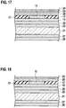
- a schematic cross-section structure of a conventional semiconductor light emitting device formed by the wafer bonding technology is expressed as shown in Fig. 23 to Fig. 25 .
- a conventional semiconductor light emitting device includes: an Au-Sn alloy layer 14 disposed on a GaAs substrate 15; a barrier metal layer 13 disposed on the Au-Sn alloy layer 14; a p type cladding layer 10 disposed on the barrier metal layer 13; an MQW layer 9 disposed on the p type cladding layer 10; an n type cladding layer 8 disposed on the MQW layer 9; and a window layer 7 disposed on the n type cladding layer 8.
- the metal used for the wafer bonding is Au-Sn alloy.
- the Au-Sn alloy since the melting point is low, the Au-Sn alloy at the side of an epitaxial growth layer composing an LED in low temperature, and the Au-Sn alloy at the side of the GaAs substrate 15 can be melted and bonded.
- another conventional semiconductor light emitting device includes: a metallic reflecting layer 16 disposed on a GaAs substrate 15; a p type cladding layer 10 disposed on the metallic reflecting layer 16; an MQW layer 9 disposed on the p type cladding layer 10; an n type cladding layer 8 disposed on the MQW layer 9; and a window layer 7 disposed on the n type cladding layer 8.
- a metallic reflecting layer 16 disposed on a GaAs substrate 15
- a p type cladding layer 10 disposed on the metallic reflecting layer 16
- an MQW layer 9 disposed on the p type cladding layer 10
- an n type cladding layer 8 disposed on the MQW layer 9
- a window layer 7 disposed on the n type cladding layer 8.
- the semiconductor LED Light Emitting Device
- a method of inserting a DBR (Distributed Bragg Reflector) layer between the GaAs substrate and the active layer (MQW) as an optical reflecting layer In order to perform high brightness of the semiconductor LED (Light Emitting Device), there is also a method of inserting a DBR (Distributed Bragg Reflector) layer between the GaAs substrate and the active layer (MQW) as an optical reflecting layer.
- the LED of the structure which does not insert the DBR becomes dark since the light which emitted in the MQW layer is absorbed by the GaAs substrate. Therefore, in order to perform the high brightness of the LED using the GaAs substrate, the DBR is used as the optical reflecting layer.
- DBR Distributed Bragg Reflector
- another conventional semiconductor light emitting device includes: a DBR layer 19 disposed on a GaAs substrate 15; ap type cladding layer 10 disposed on the DBR layer 19; an MQW layer 9 disposed on the p type cladding layer 10; an n type cladding layer 8 disposed on the MQW layer 9; and a window layer 7 disposed on the n type cladding layer 8.
- the DBR layer 19 is used as an optical reflecting layer between the GaAs substrate 15 and the MQW layer 9.
- the DBR layer 19 reflects only an incident light from a certain one way, the DBR does not reflect light if an incident angle changes, and the DBR layer 19 does not reflects an incident light from other angle and then passes through the incident light. Therefore, there is a problem that the passed through light is absorbed by the GaAs substrate 15 and the light emitting brightness of the semiconductor LED (Light Emitting Device) is reduced.
- the conventional semiconductor light emitting device formed by the wafer bonding technology needs to insert the barrier metal layer, in order to prevent the thermal diffusion of Sn, when using the Au-Sn alloy layer as a metal used for the wafer bonding. Moreover, the Au-Sn alloy layer has a wrong optical reflection factor.
- the optical absorption occurs in the interface between the metal and the semiconductor, and then the light cannot be reflected efficiently.
- the DBR layer when used as the reflecting layer, the DBR layer reflects only an incident light from a certain one way, the DBR layer does not reflect and passes through the incident light if an incident angle changes, and the incident light is absorbed by the GaAs substrate, thereby the light emitting brightness of LED is reduced.
- the purpose of the present invention is to provide a semiconductor light emitting device with the high luminance formed by performing the wafer bonding of the substrate using a non-transparent semiconductor substrate, such as GaAs and Si, and forming the metallic reflecting layer, and a fabrication method for the same.
- the purpose of a present invention is to provide a semiconductor light emitting device with the high luminance formed by avoiding the contact between a semiconductor and metal, preventing the optical absorption in the interface between the semiconductor and the metal, and forming the metallic reflecting layer having a sufficient reflection factor, by inserting a transparent insulating film between the metal and the semiconductor, and a fabrication method for the same.
- the purpose of the present invention is to provide a semiconductor light emitting device with the high luminance which is able to reflect the light of all angles by using not the DBR but a metal layer for the optical reflecting layer, and a fabrication method for the same.
- a schematic cross-section structure of a p type GaAs substrate applied to the semiconductor light emitting device and the fabrication method for the same according to the present embodiment is expressed as shown in Fig. 1 .
- a schematic cross-section structure of an n type GaAs substrate applied to the semiconductor light emitting device and the fabrication method according to the present embodiment for the same is expressed as shown in Fig. 2 .
- a schematic cross-section structure of an LED applied to the semiconductor light emitting device and a fabrication method for the same according to the present embodiment is expressed as shown in Fig. 3 .
- a schematic cross-section structure of the semiconductor light emitting device according to the present embodiment formed by bonding mutually the LED shown in Fig. 3 with the p type GaAs substrate or the n type GaAs substrate shown in Fig. 1 or Fig. 2 by wafer bonding technology is expressed as shown in Fig. 4 .
- the p type GaAs substrate applied to the semiconductor light emitting device and the fabrication method for the same includes: a p type GaAs layer 3; a metal buffer layer 2 disposed on the surface of the p type GaAs layer 3; a metal layer 1 disposed on the metal buffer layer 2; a metal buffer layer 4 disposed at the back side of the p type GaAs layer 3; and a metal layer 5 disposed on the surface of the opposite side at the side of the p type GaAs layer 3 of the metal buffer layer 4.
- the n type GaAs substrate applied to the semiconductor light emitting device and the fabrication method for the same includes: an n type GaAs layer 6; a metal buffer layer 2 disposed on the surface of the n type GaAs layer 6; a metal layer 1 disposed on the metal buffer layer 2; a metal buffer layer 4 disposed at the back side of the n type GaAs layer 6; and a metal layer 5 disposed on the surface of the opposite side at the side of the n type GaAs layer 6 of the metal buffer layer 4.
- each the metal layers 1 and 5 are formed of an Au layer, and each the metal buffer layers 2 and 4 can be all formed, for example of an AuBe layer in order to achieve the electrical contact to the p type GaAs layer 3.
- each the metal layers 1 and 5 are formed of an Au layer, and each the metal buffer layers 2 and 4 can be formed, for example of an AuGe layer in order to achieve the electrical contact to the n type GaAs layer 6.
- a schematic cross-section structure of the LED applied to the semiconductor light emitting device and the fabrication method for the same includes: a metal layer 12; a metallic contacts layer 11 disposed on the metal layer 12; a p type cladding layer 10 disposed on the metallic contacts layer 11; an MQWlayer 9 disposed on the p type cladding layer 10; an n type cladding layer 8 disposed on the MQW layer 9; and a window layer 7 disposed on the n type cladding layer 8.
- the metal layer 12 is formed, for example of an Au layer.
- the metallic contacts layer 11 is formed, for example of an AuBe layer or an alloy layer of AuBe and Ni.
- the p type cladding layer 10 is formed of an AlGaAs layer or a multilayer structure of an AlGaAs layer applying the conductivity type as p - type and an AlGaAs layer applying the conductivity type as p + type, for example, and the thickness is about 0.1 ⁇ m, for example.
- the MQW layer 9 is composed of MQW (multi-quantum well) structure laminated by about 100 pairs of heterojunction pairs composed of a GaAs/GaAlAs layer, for example, and the thickness is formed in about 1.6 ⁇ m, for example.
- the n type cladding layer 8 is formed, for example of an n type AlGaAs layer, and the thickness is about 0.1 ⁇ m, for example.
- the window layer 7 is composed, for example of a multilayer structure of an AlGaAs layer, and a GaAs layer formed on the multilayer structure of the AlGaAs layer, and the whole thickness is about 0.95 ⁇ m.
- the semiconductor light emitting device is formed by bonding mutually the LED structure shown in Fig. 3 with the p type GaAs substrate or the n type GaAs substrate shown in Fig. 1 or Fig. 2 by the wafer bonding technology.
- the semiconductor light emitting device is composed of: a p(n) type GaAs substrate structure including the p (n) type GaAs layer 3 (6), the metal buffer layer 2 disposed on the surface of the p (n) type GaAs layer 3 (6), the metal layer 1 disposed on the metal buffer layer 2, the metal buffer layer 4 disposed at the back side of the p (n) type GaAs layer 3 (6), and the metal layer 5 disposed on the surface of the opposite side at the side of the p (n) type GaAs layer 3 of the metal buffer layer 4 (6); and an LED structure disposed on the aforementioned p(n) type GaAs substrate, and including the metal layer 12, the metallic contacts layer 11 disposed on the metal layer 12, the p type cladding layer 10 disposed on the metallic contacts layer 11, the MQW layer 9 disposed on the p type cladding layer 10, the n type cladding layer 8 disposed on the MQW layer 9, and the
- the p(n) type GaAs substrate structure and the LED structure which is composed of epitaxial growth layer are bonded by using the metal layer 1 and the metal layer 12. Accordingly, it is possible to form the metallic reflecting layer which does not need a barrier metal and has a sufficient reflection factor.
- the metallic reflecting layer is beforehand formed of the metal layer 12 disposed at the LED structure side. Since a mirror surface is formed of the interface between the p type cladding layer 10 and the metal layer 12, the radiated light from the LED is reflected in the aforementioned mirror surface.
- the metallic contacts layer 11 is a layer for achieving the ohmic contact of the metal layer 12 and the p type cladding layer 10
- the metallic contacts layer 11 is intervened to the interface between the metal layer 12 and the p type cladding layer 10, and forms a part of the mirror surface.
- the semiconductor light emitting device can bond the metal layer 1 at the side of the GaAs substrate and the metal layer 12 at the side of the LED structure composed of the epitaxial growth layer by thermocompression bonding by forming both the metal layer 1 and the metal layer 12 with the Au layer.
- the conditions of wafer bonding are about 250 degrees C to 700 degrees C, for example, and are 300 degrees C to 400 degrees C preferable, and the pressure of thermocompression bonding is about 10 MPa to 20 MPa, for example.
- the metallic reflecting layer having the effective optical reflection factor can be formed on the structure at the side of the LED by using the metal layer 12 composed of Au, the high brightness of LED can be achieved.
- a schematic cross-section structure of an LED applied to a semiconductor light emitting device and a fabrication method for the same according to a second embodiment of the present invention is expressed as shown in Fig. 5 .
- a schematic cross-section structure of an LED applied to a semiconductor light emitting device and a fabrication method for the same according to a modified example of the present embodiment is expressed as shown in Fig. 6 .
- FIG. 7 A schematic cross-section structure of a semiconductor light emitting device according to the present embodiment formed by the wafer bonding technology by bonding mutually the LED shown in Fig. 6 with the p type or n type GaAs substrate 15 is expressed as shown in Fig. 7 .
- the metal layer which is composed of Au layer for example, and is disposed on the GaAs substrate 15 is omitting illustration.
- the LED applied to the semiconductor light emitting device and the fabrication method for the same includes: a metal layer 12; a patterned metallic contacts layer 11 and a patterned insulating layer 17 disposed on the metal layer 12; a p type cladding layer 10 disposed on the patterned metallic contacts layer 11 and the patterned insulating layer 17; an MQW layer 9 disposed on the p type cladding layer 10; an n type cladding layer 8 disposed on the MQW layer 9; and a window layer 7 disposed on the n type cladding layer 8.
- the metal layer 12 is formed, for example of an Au layer, and the thickness is about 2.5 to 5 ⁇ m, for example.
- the metallic contacts layer 11 is formed, for example of an AuBe layer or an alloy layer of AuBe and Ni, for example.
- the thickness equals that of the insulating layer 17, for example, and is about 450 nm.
- the insulating layer 17 is formed, for example of a silicon dioxide film, a silicon nitride film, an SiON film, an SiO x N y film, or these multilayer films.
- the p type cladding layer 10 is formed of an AlGaAs layer or a multilayer structure of an AlGaAs layer applying the conductivity type as p - type and an AlGaAs layer applying the conductivity type as p + type, for example, and the thickness is about 0.1 ⁇ m, for example.
- the MQW layer 9 is composed of anMQW (Multi-Quantum Well) structure which laminates about 100 pairs of hetero junction pairs composed of a GaAs/GaAlAs layer, for example, and the thickness is formed in about 1.6 ⁇ m, for example.
- the n type cladding layer 8 is formed, for example of an n type AlGaAs layer, and the thickness is about 0.1 ⁇ m, for example.
- the window layer 7 is composed, for example of a multilayer structure of an AlGaAs layer, and a GaAs layer formed on the multilayer structure of the AlGaAs layer, and the whole thickness is about 0.95 ⁇ m.
- the LED applied to the semiconductor light emitting device and a fabrication method for the same includes: a metal layer 12; a metal buffer layer 18 disposed on the metal layer 12; a patterned metallic contacts layer 11 and a patterned insulating layer 17 disposed on the metal buffer layer 18; a p type cladding layer 10 disposed on the patterned metallic contacts layer 11 and the patterned insulating layer 17; an MQW layer 9 disposed on the p type cladding layer 10; an n type cladding layer 8 disposed on the MQW layer 9; and a window layer 7 disposed on the n type cladding layer 8.
- the metal buffer layer 18 is formed, for example of Ag, Al, Ni, Cr, or W layer. Since blue light and ultraviolet light are absorbed in the metal layer 12 composed of Au layer, it is preferable to provide the metal buffer layer 18 composed of Ag, Al, etc. in order to reflect the light at the side of such short wavelength.
- the explanation is omitted.
- the semiconductor light emitting device is formed by bonding mutually the LED structure shown in Fig. 5 to Fig. 6 and the GaAs substrate 15 by the wafer bonding technology, as shown in Fig. 7 .
- the semiconductor light emitting device is composed of: a GaAs substrate 15; a metal layer 12 disposed on the GaAs substrate 15; a metal buffer layer 18 disposed on the metal layer 12; a patterned metallic contacts layer 11 and a patterned insulating layer 17 disposed on the metal buffer layer 18; a p type cladding layer 10 disposed on the patterned metallic contacts layer 11 and the patterned insulating layer 17; an MQW layer 9 disposed on the p type cladding layer 10; an n type cladding layer 8 disposed on the MQW layer 9; and an LED structure including a window layer 7 disposed on the n type cladding layer 8.
- the metallic reflecting layer having a sufficient reflection factor by bonding the GaAs substrate 15 and the LED structure composed of the epitaxial growth layer by using the metal layer 12.
- the metallic reflecting layer is beforehand formed of the metal layer 12 disposed at the LED structure side. Since a mirror surface is formed of the interface between the insulating layer 17, and the metal layer 12 or the metal buffer layer 18, the radiated light from the LED is reflected on the aforementioned mirror surface.
- the metallic contacts layer 11 is a layer for achieving the ohmic contact of the metal layer 12 or the metal buffer layer 18, and the p type cladding layer 10, the metallic contacts layer 11 is intervened to the interface between the metal layer 12 and the p type cladding layer 10, and has the same thickness as the insulating layer 17.
- the optimal pattern width and pattern structure exist.
- a honeycomb pattern structure based on a hexagon or a dotted pattern structure based on a round shape. Such pattern shape will be explained in relation to a fourth embodiment, referring to Fig. 13 and Fig. 14 .
- the metal layer (not shown) at the side of the GaAs substrate and the metal layer 12 at the side of the LED structure composed of the epitaxial growth layer can be bonded by thermocompression bonding by forming both the metal layer disposed on a GaAs substrate, and the metal layer 12 disposed at the LED side by the Au layer.
- the conditions of wafer bonding are about 250 degrees C to 700 degrees C, for example, and are 300 degrees C to 400 degrees C preferable, and the pressure of thermocompression bonding is about 10 MPa to 20 MPa, for example.
- the contact between the semiconductor layer, such as the p type cladding layer 10, and the metal layer 12 can be avoided, the optical absorption can be prevented, and the metallic reflecting layer having a sufficient reflection factor can be formed by forming the transparent insulating layer 17 between the metal layer 12 acting as the metallic reflecting layer or the metal buffer layer 18, and the semiconductor layer, such as the p type cladding layer 10.
- the metallic contacts layer 11 composed of AuBe etc. is vapor-deposited by lift off.
- the Au layer used for bonding with the GaAs substrate 15 on the insulating layer 17 is vapor-deposited, and the metal layer 12 is formed.
- the high brightness of LED can be achieved since the contact the semiconductor layer, such as the p type cladding layer 10, with the metal layer 12 can be avoided, the optical absorption can be prevented, and the metallic reflecting layer having the sufficient reflection factor can be formed, by intervening the transparent insulating layer 17 between the metallic reflecting layer and the semiconductor layer.
- the light of short wavelength such as ultraviolet rays having a low reflection factor
- the high brightness of LED can be achieved by forming the metal buffer layer 18 composed of Ag, Al, etc. between the insulating layer 17 and the metal layer 12.
- the semiconductor light emitting device since the light is not absorbed in the interface between the p type cladding layer and the metallic reflecting layer, the high brightness of LED can be achieved.
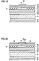
- a schematic cross-section structure of a GaAs substrate applied to a semiconductor light emitting device and a fabrication method for the same according to a third embodiment of the present invention is expressed as shown in Fig. 8 .
- a schematic cross-section structure of an LED applied to the semiconductor light emitting device and a fabrication method for the same according to the present embodiment is expressed as shown in Fig. 9 .
- a schematic cross-section structure of the semiconductor light emitting device according to the third embodiment of the present invention formed by bonding mutually the GaAs substrate 15 provided with the metal layer 20 shown in Fig. 8 and the LED shown in Fig. 9 by the wafer bonding technology is expressed as shown in Fig. 10 .
- a p type or n type GaAs substrate structure applied to a semiconductor light emitting device and the fabrication method for the same according to the present embodiment includes a GaAs substrate 15 and a metal layer 20 disposed on the surface of the GaAs substrate 15, as shown in Fig. 8 .
- the metal layer 20 is formed, for example of an Au layer.
- a schematic cross-section structure of the LED applied to the semiconductor light emitting device and the fabrication method for the same includes: a metal layer 12; a p type cladding layer 10 disposed on the metal layer 12; an MQW layer 9 disposed on the p type cladding layer 10; an n type cladding layer 8 disposed on the MQW layer 9; and a window layer 7 disposed on the n type cladding layer 8.
- the metal layer 12 is formed, for example of an Au layer, and the thickness is about 1 ⁇ m.
- the p type cladding layer 10 is formed of an AlGaAs layer or a multilayer structure of an AlGaAs layer applying the conductivity type as p - type and the AlGaAs layer applying the conductivity type as p + type, for example, and the whole thickness is formed in about 0.1 ⁇ m, for example.
- the MQW layer 9 is composed of an MQW (Multi-Quantum Well) structure which laminates about 80 to 100 pairs of heterojunction pairs composed of a GaAs/GaAlAs layer, for example, and the whole thickness is formed in about 1.6 ⁇ m, for example.
- the n type cladding layer 8 is formed, for example of an n type AlGaAs layer, and the thickness is about 0.1 ⁇ m, for example.
- the window layer 7 is composed, for example of a multilayer structure of an AlGaAs layer, and a GaAs layer formed on the multilayer structure of the AlGaAs layer, and the whole thickness is about 0.95 ⁇ m.
- the semiconductor light emitting device is formed by bonding mutually the LED structure shown in Fig. 9 with the p type or n type GaAs substrate shown in Fig. 8 by the wafer bonding technology.
- the semiconductor light emitting device is composed of : a GaAs substrate structure including the GaAs substrate 15, and the metal layer 20 disposed on the surface of the GaAs substrate 15; and an LED structure disposed on the aforementioned GaAs substrate structure and including the metal layer 12, the p type cladding layer 10 disposed on the metal layer 12, the MQW layer 9 disposed on the p type cladding layer 10, the n type cladding layer 8 disposed on the MQW layer 9, and the window layer 7 disposed on the n type cladding layer 8.
- the metallic reflecting layer is beforehand formed of the metal layer 12 disposed at the LED structure side. Since a mirror surface is formed of the interface between the p type cladding layer 10 and the metal layer 12, the radiated light from the LED is reflected in the aforementioned mirror surface.
- the semiconductor light emitting device can bond the metal layer 20 at the side of the GaAs substrate and the metal layer 12 at the side of the LED structure composed of the epitaxial growth layer by thermocompression bonding by forming both the metal layer 20 and the metal layer 12 with the Au layer.
- the conditions of wafer bonding are about 250 degrees C to 700 degrees C, for example, and are 300 degrees C to 400 degrees C preferable, and the pressure of thermocompression bonding is about 10 MPa to 20 MPa, for example.
- the semiconductor light emitting device and the fabrication method for the same has the characteristic at the point of performing total reflection of the light by using the metal for the reflecting layer in order to prevent the optical absorption to the GaAs substrate, and preventing the absorption to the GaAs substrate.
- a material of the semiconductor substrate to bond non-transparent semiconductor substrate materials, such as GaAs and Si, are used.
- the metal layer 20 and the metal layer 12 are bonding by using the Au layer as the metal layer 20 at the side of the GaAs substrate 15 and using the Au layer also as the metal layer 12 at the side of the LED including the epitaxial growth layer, and the metal layer 12 used for bonding is applied to the optical reflecting layer as the metallic reflecting layer.
- the high brightness of the LED can be performed since it is possible to perform total reflection of the light by using the metal for the reflecting layer, to prevent the absorption to the GaAs substrate, and to reflect the light of all angles, in order to prevent the optical absorption to the GaAs substrate.
- a schematic cross-section structure of a silicon substrate applied to a semiconductor light emitting device and a fabrication method for the same according to a fourth embodiment of the present invention is expressed as shown in Fig. 11 .
- a schematic cross-section structure of an LED applied to the semiconductor light emitting device and a fabrication method for the same according to the present embodiment is expressed as shown in Fig. 12 .
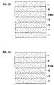
- a schematic plane pattern structure of the LED applied to the semiconductor light emitting device and the fabrication method for the same according to the present embodiment is expressed as shown in Fig. 13 .
- another schematic plane pattern structure is expressed as shown in Fig. 14 .
- the silicon substrate 21 applied to the semiconductor light emitting device and the fabrication method for the same according to the present embodiment includes a silicon substrate 21, a titanium (Ti) layer 22 disposed on the surface of the silicon substrate 21, and a metal layer 20 disposed on the surface of the titanium (Ti) layer 22.
- the thickness of the silicon substrate 21 is about 130 ⁇ m, for example.
- the metal layer 20 is formed, for example of an Au layer, and the thickness is about 2.5 ⁇ m.
- the LED applied to the semiconductor light emitting device and the fabrication method for the same includes: a GaAs substrate 23; an AlInGaP layer 24 disposed on the GaAs substrate 23; an n type GaAs layer 25 disposed on the AlInGaP layer 24; an epitaxial growth layer 26 disposed on the n type GaAs layer 25; a patterned metallic contacts layer 11 and a patterned insulating layer 17 disposed on the epitaxial growth layer 26; and a metal layer 12 disposed on the patterned metallic contacts layer 11 and the patterned insulating layer 17.
- the thickness of the GaAs substrate 23 is about 300 ⁇ m, for example, and the thickness of the AlInGaP layer 24 is about 350 nm, for example.
- the n type GaAs layer 25 functions as a contact layer between the GaAs substrate 23 and the epitaxial growth layer 26 via the AlInGaP layer 24, and the thickness is about 500 nm, for example.
- the epitaxial growth layer 26 includes: an n type window layer composed of an AlGaAs layer; an n type cladding layer; an MQW layer composed of a plurality of pairs of the heterojunction of GaAs/AlGaAs; an n type cladding layer composed of an AlGaAs layer; and a p type window layer composed of an AlGaAs layer/GaP layer.
- the MQW layer is composed of an MQW (Multi-Quantum Well) structure which laminates about 100 pairs of hetero junction pairs composed of a GaAs/GaAlAs layer, for example, and the thickness is formed in about 1.6 ⁇ m, for example.
- the metallic contacts layer 11 is formed, for example of an AuBe layer or an alloy layer of AuBe and Ni, for example.
- the thickness is the same grade as the insulating layer 17, and is about 450 nm.
- the metallic contacts layer 11 may be formed, for example as layered structure, such as Au/AuBe-Ni alloy/Au.
- the insulating layer 17 is formed, for example of a silicon dioxide film, a silicon nitride film, an SiON film, an SiO x N y film, or these multilayer films.
- the metal layer 12 is formed, for example of an Au layer, and the thickness is about 2.5 to 5 ⁇ m, for example.
- the p type cladding layer in the epitaxial growth layer 26 is formed of an AlGaAs layer or a multilayer structure of an AlGaAs layer applying the conductivity type as p - type and an AlGaAs layer applying the conductivity type as p + type, for example, and the thickness is about 0.1 ⁇ m, for example.
- the n type cladding layer in the epitaxial growth layer 26 is formed, for example of a n type AlGaAs layer, and the thickness is about 0.1 ⁇ m, for example.
- An n type window layer is composed, for example of a multilayer structure of an AlGaAs layer and a GaAs layer formed on the multilayer structure of the AlGaAs layer, and the whole thickness is about 0.95 ⁇ m, for example.
- a p type window layer is composed, for example of a multilayer structure of an AlGaAs layer and a GaP layer formed on the multilayer structure of the AlGaAs layer, and the whole thickness is about 0.32 ⁇ m, for example.
- the semiconductor light emitting device is formed by bonding mutually the silicon substrate structure shown in Fig. 11 , and the LED structure shown in Fig. 12 by the wafer bonding technology.
- the semiconductor light emitting device includes: a silicon substrate structure composed of a silicon substrate 21, a titanium layer 22 disposed on the silicon substrate 21, and a metal layer 20 disposed on the titanium layer 22; and an LED structure composed of a metal layer 12 disposed on the metal layer 20, a patterned metallic contacts layer 11 and a patterned insulating layer 17 disposed on the metal layer 12, an epitaxial growth layer 26 disposed on the patterned metallic contacts layer 11 and the patterned insulating layer 17 and having a frosting processing region 30 (region formed by performing frosting processing of the exposed n type GaAs layer 25) on the exposed surface, a patterned n type GaAs layer 25 disposed on the epitaxial growth layer 26, and a patterned surface electrode layer 29 disposed on the n type GaAs layer 25 similarly.
- a titanium layer 27 and a back surface electrode layer 28 are disposed at the back side of the silicon substrate 21.
- a blocking layer 31 for preventing current concentration may be disposed between the epitaxial growth layer 26 and the n type GaAs layer 25, as shown in Fig. 22 which are described later.
- a metallic reflecting layer having a sufficient reflection factor by bonding the silicon substrate structure and the LED structure composed of the epitaxial growth layer by using the metal layer 12.
- the metallic reflecting layer is beforehand formed of the metal layer 12 disposed at the LED structure side. Since a mirror surface is formed of the interface between the insulating layer 17 and the metal layer 12, the radiated light from the LED is reflected in the aforementioned mirror surface.
- the metallic contacts layer 11 is a layer for achieving the ohmic contact of the metal layer 12 and the epitaxial growth layer 26, the metallic contacts layer 11 is intervened to the interface between the metal layer 12 and the epitaxial growth layer 26, and has the thickness of the same grade as the insulating layer 17.
- the pattern width of the metallic contacts layer 11 Since a substantial light emitting region is limited when the pattern width of the metallic contacts layer 11 is wide, the area efficiency reduces and the light emitting efficiency decreases. On the other hand, when the pattern width of the metallic contacts layer 11 is narrow, the sheet resistivity of the metallic contacts layer 11 increases and the forward voltage Vf of LED rises. Accordingly, there are the optimal pattern width Wand the pattern pitch D1. In some examples of the pattern, there is a honeycomb pattern structure based on a hexagon or a circular dotted pattern structure based on a circular dotted shape basic structure.
- a schematic plane pattern structure of the LED applied to the semiconductor light emitting device and the fabrication method for the same according to the present embodiment has the honeycomb pattern structure based on a hexagonal basic structure, for example, as shown in Fig. 13 .
- the shaped part shown by the width W shows a pattern of the metallic contacts layer 11 formed, for example of an AuBe layer or an alloy layer of AuBe and Ni also in Fig. 12 .
- the hexagonal pattern having the width D1 is equivalent to a part of the insulating layer 17, and expresses a region where the radiated light from LED is guided.
- the width D1 is about 100 ⁇ m, for example, and the line width W is about 5 ⁇ m to about 11 ⁇ m.
- FIG. 14 Another schematic plane pattern structure of the LED applied to the semiconductor light emitting device and the fabrication method for the same according to the present embodiment has a dotted pattern structure based on a round shape, for example, as shown in Fig. 14 .
- the shaped part shown by the width d shows a pattern of the metallic contacts layer 11 formed of an AuBe layer or an alloy layer of AuBe and Ni in Fig. 12 , and is disposed by the pattern pitch having the width D2.
- the region except the circular pattern part having the width d and the pattern pitch D2 is equivalent to a part of the insulating layer 17, and expresses a region where the radiated light from LED is guided.
- the pattern pitch D2 is about 100 ⁇ m, for example, and the width d is about 5 ⁇ m to about 11 ⁇ m.
- the schematic plane pattern structure of the LED applied to the semiconductor light emitting device the fabrication method for the same according to the present embodiment is not limited to the hexagonal honeycomb pattern and the circular dotted pattern, but a random pattern for disposing a triangular pattern, a rectangular pattern, a hexagonal pattern, an octagonal pattern, a circular dotted pattern, etc. at random is also applicable.
- the schematic plane pattern structure of the LED applied to the semiconductor light emitting device according to the present embodiment has only to be able to secure the metal wiring pattern width which is a level in which the forward voltage Vf of LED does not rise without reducing the light emitting brightness from the LED securing the size of a light guide region.
- Schematic cross-section structures for explaining one process of the fabrication method of the semiconductor light emitting device according to the present embodiment is expressed as shown in Fig. 11 to Fig. 20 .
- tungsten (W) barrier metal a tungsten (W) barrier metal, a platinum (Pt) barrier metal, etc. can also be used as an alternative of the titanium layer 22 and the titanium layer 27, for example.
- W tungsten
- Pt platinum
- the semiconductor light emitting device according to the fourth embodiment of the present invention using the silicon substrate 21 is completed.
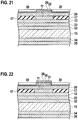
- a schematic cross-section structure for explaining one process of a fabrication method of a semiconductor light emitting device according to a modified example of the present embodiment is expressed as shown in Fig. 21 .
- a schematic cross-section structure for explaining one process of a fabrication method of a semiconductor light emitting device according to another modified example of the present embodiment is expressed as shown in Fig. 22 .
- the semiconductor light emitting device is formed by bonding mutually a silicon substrate structure shown in Fig. 11 and an LED structure shown in Fig. 12 by the wafer bonding technology, as shown in Fig. 21 .
- the semiconductor light emitting device includes: a GaAs substrate structure composed of a GaAs substrate 15, a metal buffer layer (AuGe-Ni alloy layer) 32 disposed on the GaAs substrate 15, and a metal layer (Au layer) 33 disposed on the metal buffer layer 32; and an LED structure which composed of a metal layer 12 disposed on the metal layer 33, a patterned metallic contacts layer 11 and a patterned insulating layer 17 disposed on the metal layer 12, an epitaxial growth layer 26 disposed on the patterned metallic contacts layer 11 and the patterned insulating layer 17 and having a frosting processing region 30 (region formed by performing frosting processing of the exposed n type GaAs layer 25) on the exposed surface, a patterned n type GaAs layer 25 disposed on the epitaxial growth layer 26, and a patterned surface electrode layer 29 disposed on the n type GaAs layer 25 similarly.
- a GaAs substrate structure composed of a GaAs substrate 15, a metal buffer layer (AuGe-Ni alloy layer) 32
- a metal buffer layer (AuGe-Ni alloy layer) 34 and a back surface electrode layer 35 are disposed at the back side of the GaAs substrate 15.
- a blocking layer 31 for preventing current concentration may be disposed between the epitaxial growth layer 26 and the n type GaAs layer 25.
- GaAs can be applied and the thickness is about 500 nm, for example.
- a metallic reflecting layer having a sufficient reflection factor by bonding the GaAs substrate structure and the LED structure composed of epitaxial growth layer, by using the metal layer 12.
- the metallic reflecting layer is beforehand formed of the metal layer 12 disposed at the LED structure side. Since a mirror surface is formed of the interface between the insulating layer 17 and the metal layer 12, the radiated light from the LED is reflected in the aforementioned mirror surface.
- the metallic contacts layer 11 is a layer for achieving the ohmic contact of the metal layer 12 and the epitaxial growth layer 26, the metallic contacts layer 11 is intervened to the interface between the metal layer 12 and the epitaxial growth layer 26, and has the thickness of the same grade as the insulating layer 17.
- the metal buffer layer 34 formed at the back side of the GaAs substrate 15 is formed, for example of an AuGe-Ni alloy layer, and the thickness is about 100 nm.
- the back surface electrode layer 35 is formed of an Au layer, and the thickness is about 500 nm.
- the metal buffer layer 32 formed on the surface of the GaAs substrate 15 is formed, for example of an AuGe-Ni alloy layer, and the thickness is about 100 nm.
- the metal layer 33 is formed of an Au layer, and the thickness is about 1 ⁇ m.
- a schematic plane pattern structure of LED applied to the semiconductor light emitting device and the fabrication method for the same according to the modified example of the present embodiment can also apply the same structure as Fig. 13 or Fig. 14 .
- the metal buffer layer 18 (refer to Fig. 6 ) composed of Ag, Al, etc. between the insulating layer 17 and the metal layer 12 explained in the modified example of the second embodiment, also in the semiconductor light emitting device according to the present embodiment and its modified example. It is because the light of short wavelength, such as ultraviolet rays having a low reflection factor, can be efficiently reflected at Au by forming the metal buffer layer 18 composed of Ag, Al, etc.
- the high brightness of LED can be achieved since the contact with the epitaxial growth layer 26 and the metal layer 12 can be avoided, the optical absorption can be prevented, and the metallic reflecting layer having a sufficient reflection factor can be formed by intervening the transparent insulating layer 17 between the metallic reflecting layer and the semiconductor layer.
- the light of short wavelength such as ultraviolet rays having a low reflection factor
- the metal buffer layer composed of Ag, Al, etc. between the insulating layer 17 and the metal layers 12 and 20.
- the high brightness of the LED can be achieved since the contact with the epitaxial growth layer 26 and the metal layer 12 is avoided and the light is not absorbed in the interface between the epitaxial growth layer 26 and the metallic reflecting layer.
- the high brightness of the LED can be performed since it becomes possible to perform the total reflection of the light by using the metal for the reflecting layer in order to prevent the optical absorption to the silicon substrate or the GaAs substrate, to prevent the absorption to the silicon substrate or the GaAs substrate, and to reflect the light of all angles.
- the silicon substrate and the GaAs substrate are mainly explained to the example as the semiconductor substrate, it is available enough in Ge SiGe, SiC, GaN substrate, or a GaN epitaxial substrate on SiC.
- an LD Laser Diode
- a DFB Distributed Feedback
- a DBR Distributed Bragg Reflector
- a VCSEL Vertical Cavity Surface Emitting Laser Diode
- the high brightness of the LED can be achieved since the barrier metal becomes unnecessary by bonding the epitaxial growth layer and the semiconductor substrate by using the metal layer composed of Au in order to solve the problem of Sn diffusion by Au-Sn alloy layer, and the metallic reflecting layer having a sufficient optical reflection factor can be formed in the structure at the side of the LED by using the metal layer composed of Au.
- the high brightness of the LED can be achieved since the contact with the semiconductor layer and the metallic reflecting layer can be avoided, the optical absorption in the interface between the semiconductor layer and the metallic reflecting layer can be prevented, and the metallic reflecting layer having a sufficient reflection factor can be formed, by inserting the transparent insulating film between the metallic reflecting layer and the semiconductor layer.
- the high brightness of the LED can be performed since it is possible to perform the total reflection of the light by using the metal for the reflecting layer in order to prevent the optical absorption to the GaAs substrate, to prevent the absorption to the GaAs substrate, and to reflect the light of all angles.
- the semiconductor light emitting device and the fabrication method for the same according to the embodiments of the invention can be used for whole semiconductor light emitting devices, such as an LED device having a non-transparent substrate, such as a GaAs substrate and a Si substrate, and an LD device.
Landscapes
- Led Devices (AREA)
Claims (7)
- Lichtemittierende Einrichtung des Halbleitertyps mit:einem GaAS-Subtrat (15);einer Metallschicht (12), die auf dem GaAS-Substrat (12) angeordnet ist; undeiner lichtemittierenden Diodenstruktur, die eine gemusterte Metallkontaktschicht (11) und eine gemusterte Isolationsschicht (17), die auf der Metallschicht (12) angeordnet ist, enthält,einer Mantelschicht (10) des p-Typs, die auf der gemusterten Metallkontaktschicht (11) und der gemusterten Isolationsschicht angeordnet ist;einer Mehrfachquantenwallschicht (9), die auf der Mantelschicht des p-Typs angeordnet ist,einer Mantelschicht (8) des n-Typs, die auf der Mehrfachquantenwallschicht angeordnet ist, undeiner Fensterschicht (7), die auf der Mantelschicht des n-Typs angeordnet ist, wobeidas GaAS-Substrat und die lichtemittierende Diodenstruktur unter Verwendung der Metallschicht verbunden sind, wobeidie Metallkontaktschicht (11) mit einem vorbestimmten Abstand in einer vorbestimmten Musterstruktur angeordnet ist, und eine Musterbreite der Metallkontaktschicht in einem Bereich von 5 µm bis 11 µm ist, wobeidie Isolationsschicht eine gemusterte Öffnung hat, die Isolationsschicht die Dicke hat, die im Wesentlichen genauso groß wie die der Metallkontaktschicht ist, die Metallkontaktschicht in der Öffnung der Isolationsschicht gebildet ist, wobeidie Mehrfachquantenwallschicht aus einer Mehrfachquantenwallstruktur aufgebaut ist, die durch Schichten von Heteroverbindungspaaren, die aus einer GaAs/GaAlAs-Schicht aufgebaut sind, gebildet ist, und die Isolationsschicht transparent mit Bezug auf eine Lichtemissionswellenlänge der Mehrfachquantenwallschicht ist.
- Lichtemittierende Einrichtung des Halbleitertyps nach Anspruch 1, ferner mit einer Metallpufferschicht (18), die auf der Metallschicht (12) angeordnet ist, und die zwischen der Metallschicht und der gemusterten Metallkontaktschicht (11) und der gemusterten Isolationsschicht (17) angeordnet ist.
- Lichtemittierende Einrichtung des Halbleitertyps nach Anspruch 1 oder 2, wobei eine Metallreflexionsschicht aus der Metallschicht, die vorher auf der Seite der lichtemittierenden Diodenstruktur angeordnet wird, gebildet ist.
- Lichtemittierende Einrichtung des Halbleitertyps nach einem der Ansprüche 1 bis 3, wobei von der lichtemittierenden Diodenstruktur abgestrahltes Licht auf einer Spiegelfläche, die an einer Grenzfläche zwischen der Isolationsschicht und der Metallschicht gebildet ist, reflektiert wird.
- Lichtemittierende Einrichtung des Halbleitertyps nach Anspruch 4, wobei die Metallpufferschicht, die zwischen einer Grenzfläche zwischen der Metallschicht und der Isolationsschicht eingeschoben ist, einen Teil der Spiegeloberfläche bildet.
- Herstellverfahren für eine lichtemittierende Einrichtung des Halbleitertyps mit:Vorbereiten einer Halbleitersubstratstruktur für ein Waferverbinden und eine lichtemittierende Diodenstruktur für ein Waferverbinden;Bilden einer ersten Metallschicht (20, 24) auf einem Halbleitersubstrat (15, 23) in der Halbleitersubstratstruktur;Bilden einer AlInGaP-Schicht (24) auf einem GaAs-Substrat, einer GaAs-Schicht (6) des n-Typs, und einer Schicht epitaktischen Wachstums (26) aufeinander in der lichtemittierenden Diodenstruktur;Bilden einer Metallkontaktschicht (11) und einer zweiten Metallschicht (12) für eine gemusterte Isolationsschicht (17) auf der Schicht des epitaktischen Wachstums;Verbinden der Halbleitersubstratstruktur für das Waferverbinden und der lichtemittierenden Diodenstruktur für das Waferverbinden durch Verbinden mit Thermokompression;Entfernen des GaAs-Substrats durch Ätzen;Entfernen der AlInGaP-Schicht;Durchführen einer Musterbildung auf einer Oberflächenelektrodenschicht; undEntfernen der GaAs-Schichten des n-Typs außer der GaAs-Schicht des n-Typs direkt unter der Oberflächenelektrodenschicht durch Durchführen eines Mattierungsverarbeitens, wobeidie Metallkontaktschicht mit einem vorbestimmten Abstand in einer vorbestimmten Musterstruktur angeordnet ist, und eine Musterbreite der Metallkontaktschicht innerhalb eines Bereiches von 5 µm bis 11 µm ist, wobeidie Isolationsschicht eine gemusterte Öffnung hat, die Isolationsschicht die Dicke aufweist, die im Wesentlichen so groß ist wie die der Metallkontaktschicht, die Metallkontaktschicht in der Öffnung der Isolationsschicht gebildet ist, und die Metallkontaktschicht aus einem Metall einschließlich Au gebildet ist, wobeidie epitaktische Wachstumsschicht eine Mehrfachquantenwallschicht (9) enthält, die aus einer Mehrfachquantenwallstruktur, die durch Schichten eines Heteroverbindungspaares, das aus einer GaAs/GaAlAs-Schicht aufgebaut ist, gebildet ist, enthält, und die Isolationsschicht transparent mit Bezug auf eine lichtemittierende Wellenlänge von der Mehrfachquantenwallschicht ist.
- Herstellverfahren für die lichtemittierende Einrichtung des Halbleitertyps nach Anspruch 6, ferner mit einem Bilden einer Blockierungsschicht (31), um eine Stromkonzentration zu verhindern, bevor das Musterbilden auf der Oberflächenelektrodenschicht nach dem Entfernen der AlInGaP-Schicht durchgeführt wird.
Applications Claiming Priority (2)
| Application Number | Priority Date | Filing Date | Title |
|---|---|---|---|
| JP2007107130A JP5346443B2 (ja) | 2007-04-16 | 2007-04-16 | 半導体発光素子およびその製造方法 |
| PCT/JP2008/057176 WO2008129963A1 (ja) | 2007-04-16 | 2008-04-11 | 半導体発光素子およびその製造方法 |
Publications (3)
| Publication Number | Publication Date |
|---|---|
| EP2139052A1 EP2139052A1 (de) | 2009-12-30 |
| EP2139052A4 EP2139052A4 (de) | 2014-01-01 |
| EP2139052B1 true EP2139052B1 (de) | 2018-11-21 |
Family
ID=39875491
Family Applications (1)
| Application Number | Title | Priority Date | Filing Date |
|---|---|---|---|
| EP08740273.1A Active EP2139052B1 (de) | 2007-04-16 | 2008-04-11 | Lichtemittierende halbleitervorrichtung und verfahren zu ihrer herstellung |
Country Status (7)
| Country | Link |
|---|---|
| US (10) | US8106412B2 (de) |
| EP (1) | EP2139052B1 (de) |
| JP (1) | JP5346443B2 (de) |
| KR (1) | KR101446370B1 (de) |
| CN (2) | CN104409588B (de) |
| TW (1) | TWI481065B (de) |
| WO (1) | WO2008129963A1 (de) |
Families Citing this family (22)
| Publication number | Priority date | Publication date | Assignee | Title |
|---|---|---|---|---|
| JP5346443B2 (ja) | 2007-04-16 | 2013-11-20 | ローム株式会社 | 半導体発光素子およびその製造方法 |
| WO2009129353A1 (en) * | 2008-04-15 | 2009-10-22 | Purdue Research Foundation | Metallized silicon substrate for indium gallium nitride light-emitting diode |
| KR101363022B1 (ko) * | 2008-12-23 | 2014-02-14 | 삼성디스플레이 주식회사 | 유기 발광 표시 장치 |
| KR100999726B1 (ko) | 2009-05-04 | 2010-12-08 | 엘지이노텍 주식회사 | 발광소자 및 그 제조방법 |
| JP2011129724A (ja) * | 2009-12-18 | 2011-06-30 | Dowa Electronics Materials Co Ltd | 半導体発光素子およびその製造方法 |
| TW201145577A (en) * | 2010-06-11 | 2011-12-16 | Hon Hai Prec Ind Co Ltd | Light-emitting diode unit and method for making it |
| CN102280552B (zh) * | 2010-06-14 | 2015-06-03 | 鸿富锦精密工业(深圳)有限公司 | 发光二极管晶粒及其制作方法 |
| US9269870B2 (en) | 2011-03-17 | 2016-02-23 | Epistar Corporation | Light-emitting device with intermediate layer |
| US9601657B2 (en) * | 2011-03-17 | 2017-03-21 | Epistar Corporation | Light-emitting device |
| US8686398B2 (en) | 2012-03-02 | 2014-04-01 | Kabushiki Kaisha Toshiba | Semiconductor light emitting device |
| US9450152B2 (en) * | 2012-05-29 | 2016-09-20 | Micron Technology, Inc. | Solid state transducer dies having reflective features over contacts and associated systems and methods |
| JP2014022401A (ja) | 2012-07-12 | 2014-02-03 | Toshiba Corp | 窒化物半導体発光素子 |
| JP5954185B2 (ja) * | 2012-12-04 | 2016-07-20 | 日亜化学工業株式会社 | 半導体素子の製造方法 |
| TWI613838B (zh) * | 2014-03-06 | 2018-02-01 | 晶元光電股份有限公司 | 發光元件 |
| CN104502878B (zh) * | 2014-12-26 | 2018-07-31 | 中国电子科技集团公司第十三研究所 | 微波GaAs衬底在片S参数微带线TRL校准件 |
| CN105785304B (zh) * | 2016-05-11 | 2018-09-18 | 中国电子科技集团公司第十三研究所 | 用于校准在片高值电阻测量系统的标准件 |
| JP6669144B2 (ja) * | 2016-12-16 | 2020-03-18 | 日亜化学工業株式会社 | 発光素子の製造方法 |
| DE102017115252A1 (de) * | 2017-07-07 | 2019-01-10 | Osram Opto Semiconductors Gmbh | Verfahren zur Herstellung eines Schichtstapels und Schichtstapel |
| JP7308831B2 (ja) * | 2017-12-14 | 2023-07-14 | ルミレッズ リミテッド ライアビリティ カンパニー | Ledダイの汚染を防止する方法 |
| US10522708B2 (en) | 2017-12-14 | 2019-12-31 | Lumileds Llc | Method of preventing contamination of LED die |
| JP2021012936A (ja) * | 2019-07-05 | 2021-02-04 | 株式会社ディスコ | 光デバイスの移設方法 |
| TWI763377B (zh) * | 2021-03-16 | 2022-05-01 | 兆勁科技股份有限公司 | 發光元件 |
Family Cites Families (49)
| Publication number | Priority date | Publication date | Assignee | Title |
|---|---|---|---|---|
| US5376580A (en) | 1993-03-19 | 1994-12-27 | Hewlett-Packard Company | Wafer bonding of light emitting diode layers |
| JP3511970B2 (ja) * | 1995-06-15 | 2004-03-29 | 日亜化学工業株式会社 | 窒化物半導体発光素子 |
| DE19537544A1 (de) * | 1995-10-09 | 1997-04-10 | Telefunken Microelectron | Lumineszenzdiode mit verbesserter Lichtausbeute |
| US5917202A (en) * | 1995-12-21 | 1999-06-29 | Hewlett-Packard Company | Highly reflective contacts for light emitting semiconductor devices |
| US6608330B1 (en) * | 1998-09-21 | 2003-08-19 | Nichia Corporation | Light emitting device |
| US6803596B2 (en) * | 1999-12-27 | 2004-10-12 | Sanyo Electric Co., Ltd. | Light emitting device |
| US6586762B2 (en) * | 2000-07-07 | 2003-07-01 | Nichia Corporation | Nitride semiconductor device with improved lifetime and high output power |
| US6803604B2 (en) * | 2001-03-13 | 2004-10-12 | Ricoh Company, Ltd. | Semiconductor optical modulator, an optical amplifier and an integrated semiconductor light-emitting device |
| TW541710B (en) * | 2001-06-27 | 2003-07-11 | Epistar Corp | LED having transparent substrate and the manufacturing method thereof |
| JP4833456B2 (ja) | 2001-08-28 | 2011-12-07 | 古河電気工業株式会社 | 半導体デバイスの製造方法 |
| US6784462B2 (en) | 2001-12-13 | 2004-08-31 | Rensselaer Polytechnic Institute | Light-emitting diode with planar omni-directional reflector |
| JP3782357B2 (ja) | 2002-01-18 | 2006-06-07 | 株式会社東芝 | 半導体発光素子の製造方法 |
| DE10239045A1 (de) * | 2002-08-26 | 2004-03-11 | Osram Opto Semiconductors Gmbh | Verfahren zum Herstellen eines elektromagnetische Strahlung emittierenden Halbleiterchips und elektromagnetische Strahlung emittierender Halbleiterchip |
| JP4004378B2 (ja) | 2002-10-24 | 2007-11-07 | ローム株式会社 | 半導体発光素子 |
| TWI230472B (en) * | 2002-11-29 | 2005-04-01 | Sanken Electric Co Ltd | Semiconductor light emitting device and the manufacturing method thereof |
| US20050205886A1 (en) * | 2002-11-29 | 2005-09-22 | Sanken Electric Co., Ltd. | Gallium-containing light-emitting semiconductor device and method of fabrication |
| JP2003282946A (ja) | 2003-02-06 | 2003-10-03 | Matsushita Electric Ind Co Ltd | 発光ダイオード装置及びその製造方法 |
| TWI230473B (en) | 2003-03-10 | 2005-04-01 | Sanken Electric Co Ltd | Semiconductor light emitting device and manufacturing method thereof |
| US20040227151A1 (en) * | 2003-03-31 | 2004-11-18 | Hitachi Cable, Ltd. | Light emitting diode |
| JP2005123530A (ja) * | 2003-10-20 | 2005-05-12 | Shin Etsu Handotai Co Ltd | 発光素子の製造方法 |
| US7704763B2 (en) * | 2003-12-09 | 2010-04-27 | The Regents Of The University Of California | Highly efficient group-III nitride based light emitting diodes via fabrication of structures on an N-face surface |
| JP2005259820A (ja) * | 2004-03-09 | 2005-09-22 | Sharp Corp | Iii−v族化合物半導体発光素子とその製造方法 |
| TWM255518U (en) * | 2004-04-23 | 2005-01-11 | Super Nova Optoelectronics Cor | Vertical electrode structure of Gallium Nitride based LED |
| JP4154731B2 (ja) * | 2004-04-27 | 2008-09-24 | 信越半導体株式会社 | 発光素子の製造方法及び発光素子 |
| US8049243B2 (en) * | 2004-05-26 | 2011-11-01 | Showa Denko K.K. | Gallium nitride-based compound semiconductor light emitting device |
| US7508001B2 (en) * | 2004-06-21 | 2009-03-24 | Panasonic Corporation | Semiconductor laser device and manufacturing method thereof |
| JP2006013381A (ja) | 2004-06-29 | 2006-01-12 | Shin Etsu Handotai Co Ltd | 発光素子 |
| JP4644193B2 (ja) | 2004-07-12 | 2011-03-02 | ローム株式会社 | 半導体発光素子 |
| JP4592388B2 (ja) * | 2004-11-04 | 2010-12-01 | シャープ株式会社 | Iii−v族化合物半導体発光素子およびその製造方法 |
| US8097897B2 (en) * | 2005-06-21 | 2012-01-17 | Epistar Corporation | High-efficiency light-emitting device and manufacturing method thereof |
| US7510768B2 (en) | 2005-06-17 | 2009-03-31 | Eastman Chemical Company | Thermoplastic articles comprising cyclobutanediol having a decorative material embedded therein |
| JP4899348B2 (ja) * | 2005-05-31 | 2012-03-21 | 信越半導体株式会社 | 発光素子の製造方法 |
| JP2007012688A (ja) * | 2005-06-28 | 2007-01-18 | Toshiba Corp | 半導体発光素子 |
| JP4970265B2 (ja) | 2005-08-03 | 2012-07-04 | スタンレー電気株式会社 | 半導体発光素子及びその製造方法 |
| JP4362125B2 (ja) * | 2006-03-15 | 2009-11-11 | ローム株式会社 | 側面発光半導体素子及び側面発光半導体素子の製造方法 |
| JP2008047672A (ja) * | 2006-08-14 | 2008-02-28 | Sumitomo Electric Ind Ltd | 半導体光素子 |
| JP4462251B2 (ja) * | 2006-08-17 | 2010-05-12 | 日立電線株式会社 | Iii−v族窒化物系半導体基板及びiii−v族窒化物系発光素子 |
| JP4835377B2 (ja) | 2006-10-20 | 2011-12-14 | 日立電線株式会社 | 半導体発光素子 |
| JP5346443B2 (ja) * | 2007-04-16 | 2013-11-20 | ローム株式会社 | 半導体発光素子およびその製造方法 |
| US8546818B2 (en) * | 2007-06-12 | 2013-10-01 | SemiLEDs Optoelectronics Co., Ltd. | Vertical LED with current-guiding structure |
| JP5123573B2 (ja) * | 2007-06-13 | 2013-01-23 | ローム株式会社 | 半導体発光素子およびその製造方法 |
| US8124991B2 (en) * | 2007-07-26 | 2012-02-28 | The Regents Of The University Of California | Light emitting diodes with a P-type surface bonded to a transparent submount to increase light extraction efficiency |
| US9634191B2 (en) * | 2007-11-14 | 2017-04-25 | Cree, Inc. | Wire bond free wafer level LED |
| KR100975659B1 (ko) * | 2007-12-18 | 2010-08-17 | 포항공과대학교 산학협력단 | 발광 소자 및 그 제조 방법 |
| JP2009200178A (ja) * | 2008-02-20 | 2009-09-03 | Hitachi Cable Ltd | 半導体発光素子 |
| US8179937B2 (en) * | 2009-01-08 | 2012-05-15 | Quantum Electro Opto Systems Sdn. Bhd. | High speed light emitting semiconductor methods and devices |
| JP4375497B1 (ja) * | 2009-03-11 | 2009-12-02 | 住友電気工業株式会社 | Iii族窒化物半導体素子、エピタキシャル基板、及びiii族窒化物半導体素子を作製する方法 |
| US7906795B2 (en) * | 2009-05-08 | 2011-03-15 | Epistar Corporation | Light-emitting device |
| JP2014120695A (ja) * | 2012-12-19 | 2014-06-30 | Rohm Co Ltd | 半導体発光素子 |
-
2007
- 2007-04-16 JP JP2007107130A patent/JP5346443B2/ja active Active
-
2008
- 2008-04-11 CN CN201410587684.XA patent/CN104409588B/zh active Active
- 2008-04-11 EP EP08740273.1A patent/EP2139052B1/de active Active
- 2008-04-11 CN CN200880012118A patent/CN101657912A/zh active Pending
- 2008-04-11 WO PCT/JP2008/057176 patent/WO2008129963A1/ja not_active Ceased
- 2008-04-11 KR KR1020097023683A patent/KR101446370B1/ko active Active
- 2008-04-11 US US12/596,004 patent/US8106412B2/en active Active
- 2008-04-15 TW TW097113675A patent/TWI481065B/zh not_active IP Right Cessation
-
2011
- 2011-12-16 US US13/327,860 patent/US8536598B2/en active Active
-
2013
- 2013-09-12 US US14/024,696 patent/US9018650B2/en active Active
-
2014
- 2014-05-23 US US14/286,696 patent/US9196808B2/en active Active
-
2015
- 2015-10-30 US US14/928,349 patent/US9450145B2/en active Active
-
2016
- 2016-08-26 US US15/248,332 patent/US9786819B2/en active Active
-
2017
- 2017-09-26 US US15/716,452 patent/US10032961B2/en active Active
-
2018
- 2018-06-22 US US16/015,282 patent/US10483435B2/en active Active
-
2019
- 2019-10-18 US US16/657,403 patent/US11616172B2/en active Active
-
2023
- 2023-02-15 US US18/169,555 patent/US20230197906A1/en active Pending
Non-Patent Citations (1)
| Title |
|---|
| None * |
Also Published As
| Publication number | Publication date |
|---|---|
| KR20090130127A (ko) | 2009-12-17 |
| US20100133507A1 (en) | 2010-06-03 |
| US9786819B2 (en) | 2017-10-10 |
| US20140008610A1 (en) | 2014-01-09 |
| US8536598B2 (en) | 2013-09-17 |
| US20140264267A1 (en) | 2014-09-18 |
| EP2139052A1 (de) | 2009-12-30 |
| JP5346443B2 (ja) | 2013-11-20 |
| JP2008270261A (ja) | 2008-11-06 |
| CN104409588A (zh) | 2015-03-11 |
| US11616172B2 (en) | 2023-03-28 |
| US20160365489A1 (en) | 2016-12-15 |
| US9196808B2 (en) | 2015-11-24 |
| US8106412B2 (en) | 2012-01-31 |
| US20180301599A1 (en) | 2018-10-18 |
| US20230197906A1 (en) | 2023-06-22 |
| TW200847492A (en) | 2008-12-01 |
| US20160056332A1 (en) | 2016-02-25 |
| US9018650B2 (en) | 2015-04-28 |
| US10483435B2 (en) | 2019-11-19 |
| EP2139052A4 (de) | 2014-01-01 |
| US20200052163A1 (en) | 2020-02-13 |
| KR101446370B1 (ko) | 2014-10-01 |
| CN104409588B (zh) | 2017-05-31 |
| US20120132889A1 (en) | 2012-05-31 |
| US10032961B2 (en) | 2018-07-24 |
| US20180019381A1 (en) | 2018-01-18 |
| TWI481065B (zh) | 2015-04-11 |
| US9450145B2 (en) | 2016-09-20 |
| WO2008129963A1 (ja) | 2008-10-30 |
| CN101657912A (zh) | 2010-02-24 |
Similar Documents
| Publication | Publication Date | Title |
|---|---|---|
| US20230197906A1 (en) | Semiconductor light emitting device | |
| EP2157623B1 (de) | Halbleiter-leuchtelement und verfahren zu seiner herstellung | |
| JP4907842B2 (ja) | 平面全方位リフレクタを有する発光ダイオード | |
| JP2002217450A (ja) | 半導体発光素子及びその製造方法 | |
| KR20090111862A (ko) | 광전 반도체칩 및 이러한 반도체칩을 위한 접촉 구조의 형성 방법 | |
| JP5584331B2 (ja) | 半導体発光素子 | |
| KR100564303B1 (ko) | AlGaInP계 발광 다이오드 및 그 제조방법 | |
| JP5396526B2 (ja) | 半導体発光素子 | |
| JP5981493B2 (ja) | 半導体発光素子 |
Legal Events
| Date | Code | Title | Description |
|---|---|---|---|
| PUAI | Public reference made under article 153(3) epc to a published international application that has entered the european phase |
Free format text: ORIGINAL CODE: 0009012 |
|
| 17P | Request for examination filed |
Effective date: 20091015 |
|
| AK | Designated contracting states |
Kind code of ref document: A1 Designated state(s): AT BE BG CH CY CZ DE DK EE ES FI FR GB GR HR HU IE IS IT LI LT LU LV MC MT NL NO PL PT RO SE SI SK TR |
|
| DAX | Request for extension of the european patent (deleted) | ||
| A4 | Supplementary search report drawn up and despatched |
Effective date: 20131128 |
|
| RIC1 | Information provided on ipc code assigned before grant |
Ipc: H01L 33/00 20100101AFI20131122BHEP Ipc: H01L 33/40 20100101ALI20131122BHEP Ipc: H01L 33/30 20100101ALN20131122BHEP |
|
| STAA | Information on the status of an ep patent application or granted ep patent |
Free format text: STATUS: EXAMINATION IS IN PROGRESS |
|
| 17Q | First examination report despatched |
Effective date: 20170918 |
|
| GRAP | Despatch of communication of intention to grant a patent |
Free format text: ORIGINAL CODE: EPIDOSNIGR1 |
|
| STAA | Information on the status of an ep patent application or granted ep patent |
Free format text: STATUS: GRANT OF PATENT IS INTENDED |
|
| RIC1 | Information provided on ipc code assigned before grant |
Ipc: H01L 33/30 20100101ALN20180504BHEP Ipc: H01L 33/46 20100101ALN20180504BHEP Ipc: H01L 33/38 20100101ALN20180504BHEP Ipc: H01L 33/00 20060101AFI20180504BHEP Ipc: H01L 33/40 20100101ALI20180504BHEP |
|
| INTG | Intention to grant announced |
Effective date: 20180530 |
|
| GRAS | Grant fee paid |
Free format text: ORIGINAL CODE: EPIDOSNIGR3 |
|
| GRAA | (expected) grant |
Free format text: ORIGINAL CODE: 0009210 |
|
| STAA | Information on the status of an ep patent application or granted ep patent |
Free format text: STATUS: THE PATENT HAS BEEN GRANTED |
|
| AK | Designated contracting states |
Kind code of ref document: B1 Designated state(s): AT BE BG CH CY CZ DE DK EE ES FI FR GB GR HR HU IE IS IT LI LT LU LV MC MT NL NO PL PT RO SE SI SK TR |
|
| REG | Reference to a national code |
Ref country code: CH Ref legal event code: EP |
|
| REG | Reference to a national code |
Ref country code: IE Ref legal event code: FG4D |
|
| REG | Reference to a national code |
Ref country code: DE Ref legal event code: R096 Ref document number: 602008058007 Country of ref document: DE |
|
| REG | Reference to a national code |
Ref country code: AT Ref legal event code: REF Ref document number: 1068554 Country of ref document: AT Kind code of ref document: T Effective date: 20181215 |
|
| REG | Reference to a national code |
Ref country code: NL Ref legal event code: MP Effective date: 20181121 |
|
| REG | Reference to a national code |
Ref country code: AT Ref legal event code: MK05 Ref document number: 1068554 Country of ref document: AT Kind code of ref document: T Effective date: 20181121 |
|
| PG25 | Lapsed in a contracting state [announced via postgrant information from national office to epo] |
Ref country code: HR Free format text: LAPSE BECAUSE OF FAILURE TO SUBMIT A TRANSLATION OF THE DESCRIPTION OR TO PAY THE FEE WITHIN THE PRESCRIBED TIME-LIMIT Effective date: 20181121 Ref country code: AT Free format text: LAPSE BECAUSE OF FAILURE TO SUBMIT A TRANSLATION OF THE DESCRIPTION OR TO PAY THE FEE WITHIN THE PRESCRIBED TIME-LIMIT Effective date: 20181121 Ref country code: NO Free format text: LAPSE BECAUSE OF FAILURE TO SUBMIT A TRANSLATION OF THE DESCRIPTION OR TO PAY THE FEE WITHIN THE PRESCRIBED TIME-LIMIT Effective date: 20190221 Ref country code: LV Free format text: LAPSE BECAUSE OF FAILURE TO SUBMIT A TRANSLATION OF THE DESCRIPTION OR TO PAY THE FEE WITHIN THE PRESCRIBED TIME-LIMIT Effective date: 20181121 Ref country code: FI Free format text: LAPSE BECAUSE OF FAILURE TO SUBMIT A TRANSLATION OF THE DESCRIPTION OR TO PAY THE FEE WITHIN THE PRESCRIBED TIME-LIMIT Effective date: 20181121 Ref country code: ES Free format text: LAPSE BECAUSE OF FAILURE TO SUBMIT A TRANSLATION OF THE DESCRIPTION OR TO PAY THE FEE WITHIN THE PRESCRIBED TIME-LIMIT Effective date: 20181121 Ref country code: BG Free format text: LAPSE BECAUSE OF FAILURE TO SUBMIT A TRANSLATION OF THE DESCRIPTION OR TO PAY THE FEE WITHIN THE PRESCRIBED TIME-LIMIT Effective date: 20190221 Ref country code: IS Free format text: LAPSE BECAUSE OF FAILURE TO SUBMIT A TRANSLATION OF THE DESCRIPTION OR TO PAY THE FEE WITHIN THE PRESCRIBED TIME-LIMIT Effective date: 20190321 Ref country code: LT Free format text: LAPSE BECAUSE OF FAILURE TO SUBMIT A TRANSLATION OF THE DESCRIPTION OR TO PAY THE FEE WITHIN THE PRESCRIBED TIME-LIMIT Effective date: 20181121 |
|
| PG25 | Lapsed in a contracting state [announced via postgrant information from national office to epo] |
Ref country code: GR Free format text: LAPSE BECAUSE OF FAILURE TO SUBMIT A TRANSLATION OF THE DESCRIPTION OR TO PAY THE FEE WITHIN THE PRESCRIBED TIME-LIMIT Effective date: 20190222 Ref country code: NL Free format text: LAPSE BECAUSE OF FAILURE TO SUBMIT A TRANSLATION OF THE DESCRIPTION OR TO PAY THE FEE WITHIN THE PRESCRIBED TIME-LIMIT Effective date: 20181121 Ref country code: PT Free format text: LAPSE BECAUSE OF FAILURE TO SUBMIT A TRANSLATION OF THE DESCRIPTION OR TO PAY THE FEE WITHIN THE PRESCRIBED TIME-LIMIT Effective date: 20190321 Ref country code: SE Free format text: LAPSE BECAUSE OF FAILURE TO SUBMIT A TRANSLATION OF THE DESCRIPTION OR TO PAY THE FEE WITHIN THE PRESCRIBED TIME-LIMIT Effective date: 20181121 |
|
| PG25 | Lapsed in a contracting state [announced via postgrant information from national office to epo] |
Ref country code: PL Free format text: LAPSE BECAUSE OF FAILURE TO SUBMIT A TRANSLATION OF THE DESCRIPTION OR TO PAY THE FEE WITHIN THE PRESCRIBED TIME-LIMIT Effective date: 20181121 Ref country code: CZ Free format text: LAPSE BECAUSE OF FAILURE TO SUBMIT A TRANSLATION OF THE DESCRIPTION OR TO PAY THE FEE WITHIN THE PRESCRIBED TIME-LIMIT Effective date: 20181121 Ref country code: IT Free format text: LAPSE BECAUSE OF FAILURE TO SUBMIT A TRANSLATION OF THE DESCRIPTION OR TO PAY THE FEE WITHIN THE PRESCRIBED TIME-LIMIT Effective date: 20181121 Ref country code: DK Free format text: LAPSE BECAUSE OF FAILURE TO SUBMIT A TRANSLATION OF THE DESCRIPTION OR TO PAY THE FEE WITHIN THE PRESCRIBED TIME-LIMIT Effective date: 20181121 |
|
| REG | Reference to a national code |
Ref country code: DE Ref legal event code: R097 Ref document number: 602008058007 Country of ref document: DE |
|
| PG25 | Lapsed in a contracting state [announced via postgrant information from national office to epo] |
Ref country code: EE Free format text: LAPSE BECAUSE OF FAILURE TO SUBMIT A TRANSLATION OF THE DESCRIPTION OR TO PAY THE FEE WITHIN THE PRESCRIBED TIME-LIMIT Effective date: 20181121 Ref country code: SK Free format text: LAPSE BECAUSE OF FAILURE TO SUBMIT A TRANSLATION OF THE DESCRIPTION OR TO PAY THE FEE WITHIN THE PRESCRIBED TIME-LIMIT Effective date: 20181121 Ref country code: RO Free format text: LAPSE BECAUSE OF FAILURE TO SUBMIT A TRANSLATION OF THE DESCRIPTION OR TO PAY THE FEE WITHIN THE PRESCRIBED TIME-LIMIT Effective date: 20181121 |
|
| PLBE | No opposition filed within time limit |
Free format text: ORIGINAL CODE: 0009261 |
|
| STAA | Information on the status of an ep patent application or granted ep patent |
Free format text: STATUS: NO OPPOSITION FILED WITHIN TIME LIMIT |
|
| 26N | No opposition filed |
Effective date: 20190822 |
|
| PG25 | Lapsed in a contracting state [announced via postgrant information from national office to epo] |
Ref country code: SI Free format text: LAPSE BECAUSE OF FAILURE TO SUBMIT A TRANSLATION OF THE DESCRIPTION OR TO PAY THE FEE WITHIN THE PRESCRIBED TIME-LIMIT Effective date: 20181121 |
|
| REG | Reference to a national code |
Ref country code: CH Ref legal event code: PL |
|
| REG | Reference to a national code |
Ref country code: BE Ref legal event code: MM Effective date: 20190430 |
|
| GBPC | Gb: european patent ceased through non-payment of renewal fee |
Effective date: 20190411 |
|
| PG25 | Lapsed in a contracting state [announced via postgrant information from national office to epo] |
Ref country code: MC Free format text: LAPSE BECAUSE OF FAILURE TO SUBMIT A TRANSLATION OF THE DESCRIPTION OR TO PAY THE FEE WITHIN THE PRESCRIBED TIME-LIMIT Effective date: 20181121 Ref country code: LU Free format text: LAPSE BECAUSE OF NON-PAYMENT OF DUE FEES Effective date: 20190411 |
|
| PG25 | Lapsed in a contracting state [announced via postgrant information from national office to epo] |
Ref country code: LI Free format text: LAPSE BECAUSE OF NON-PAYMENT OF DUE FEES Effective date: 20190430 Ref country code: CH Free format text: LAPSE BECAUSE OF NON-PAYMENT OF DUE FEES Effective date: 20190430 Ref country code: GB Free format text: LAPSE BECAUSE OF NON-PAYMENT OF DUE FEES Effective date: 20190411 |
|
| PG25 | Lapsed in a contracting state [announced via postgrant information from national office to epo] |
Ref country code: BE Free format text: LAPSE BECAUSE OF NON-PAYMENT OF DUE FEES Effective date: 20190430 |
|
| PG25 | Lapsed in a contracting state [announced via postgrant information from national office to epo] |
Ref country code: TR Free format text: LAPSE BECAUSE OF FAILURE TO SUBMIT A TRANSLATION OF THE DESCRIPTION OR TO PAY THE FEE WITHIN THE PRESCRIBED TIME-LIMIT Effective date: 20181121 |
|
| PG25 | Lapsed in a contracting state [announced via postgrant information from national office to epo] |
Ref country code: IE Free format text: LAPSE BECAUSE OF NON-PAYMENT OF DUE FEES Effective date: 20190411 |
|
| PG25 | Lapsed in a contracting state [announced via postgrant information from national office to epo] |
Ref country code: FR Free format text: LAPSE BECAUSE OF NON-PAYMENT OF DUE FEES Effective date: 20190430 |
|
| PG25 | Lapsed in a contracting state [announced via postgrant information from national office to epo] |
Ref country code: CY Free format text: LAPSE BECAUSE OF FAILURE TO SUBMIT A TRANSLATION OF THE DESCRIPTION OR TO PAY THE FEE WITHIN THE PRESCRIBED TIME-LIMIT Effective date: 20181121 |
|
| PG25 | Lapsed in a contracting state [announced via postgrant information from national office to epo] |
Ref country code: HU Free format text: LAPSE BECAUSE OF FAILURE TO SUBMIT A TRANSLATION OF THE DESCRIPTION OR TO PAY THE FEE WITHIN THE PRESCRIBED TIME-LIMIT; INVALID AB INITIO Effective date: 20080411 Ref country code: MT Free format text: LAPSE BECAUSE OF FAILURE TO SUBMIT A TRANSLATION OF THE DESCRIPTION OR TO PAY THE FEE WITHIN THE PRESCRIBED TIME-LIMIT Effective date: 20181121 |
|
| P01 | Opt-out of the competence of the unified patent court (upc) registered |
Effective date: 20230512 |
|
| REG | Reference to a national code |
Ref country code: DE Ref legal event code: R079 Ref document number: 602008058007 Country of ref document: DE Free format text: PREVIOUS MAIN CLASS: H01L0033000000 Ipc: H10H0020000000 |
|
| PGFP | Annual fee paid to national office [announced via postgrant information from national office to epo] |
Ref country code: DE Payment date: 20250305 Year of fee payment: 18 |