EP2138932B1 - Prozessor zur Ausführung von hochwirksamen VLIW-Befehlen - Google Patents
Prozessor zur Ausführung von hochwirksamen VLIW-Befehlen Download PDFInfo
- Publication number
- EP2138932B1 EP2138932B1 EP09172121A EP09172121A EP2138932B1 EP 2138932 B1 EP2138932 B1 EP 2138932B1 EP 09172121 A EP09172121 A EP 09172121A EP 09172121 A EP09172121 A EP 09172121A EP 2138932 B1 EP2138932 B1 EP 2138932B1
- Authority
- EP
- European Patent Office
- Prior art keywords
- instruction
- field
- constant
- register
- unit
- Prior art date
- Legal status (The legal status is an assumption and is not a legal conclusion. Google has not performed a legal analysis and makes no representation as to the accuracy of the status listed.)
- Expired - Lifetime
Links
- 238000010276 construction Methods 0.000 description 27
- 238000000034 method Methods 0.000 description 26
- 238000012546 transfer Methods 0.000 description 16
- 238000012545 processing Methods 0.000 description 11
- 238000012986 modification Methods 0.000 description 8
- 230000004048 modification Effects 0.000 description 8
- 238000010586 diagram Methods 0.000 description 7
- 230000002093 peripheral effect Effects 0.000 description 4
- 238000006073 displacement reaction Methods 0.000 description 3
- 230000001343 mnemonic effect Effects 0.000 description 3
- 230000007423 decrease Effects 0.000 description 2
- 230000000694 effects Effects 0.000 description 1
- 238000003780 insertion Methods 0.000 description 1
- 230000037431 insertion Effects 0.000 description 1
Images


Classifications
-
- G—PHYSICS
- G06—COMPUTING; CALCULATING OR COUNTING
- G06F—ELECTRIC DIGITAL DATA PROCESSING
- G06F9/00—Arrangements for program control, e.g. control units
-
- G—PHYSICS
- G06—COMPUTING; CALCULATING OR COUNTING
- G06F—ELECTRIC DIGITAL DATA PROCESSING
- G06F9/00—Arrangements for program control, e.g. control units
- G06F9/06—Arrangements for program control, e.g. control units using stored programs, i.e. using an internal store of processing equipment to receive or retain programs
- G06F9/30—Arrangements for executing machine instructions, e.g. instruction decode
- G06F9/38—Concurrent instruction execution, e.g. pipeline, look ahead
- G06F9/3818—Decoding for concurrent execution
- G06F9/3822—Parallel decoding, e.g. parallel decode units
-
- G—PHYSICS
- G06—COMPUTING; CALCULATING OR COUNTING
- G06F—ELECTRIC DIGITAL DATA PROCESSING
- G06F9/00—Arrangements for program control, e.g. control units
- G06F9/06—Arrangements for program control, e.g. control units using stored programs, i.e. using an internal store of processing equipment to receive or retain programs
- G06F9/30—Arrangements for executing machine instructions, e.g. instruction decode
- G06F9/30145—Instruction analysis, e.g. decoding, instruction word fields
- G06F9/30149—Instruction analysis, e.g. decoding, instruction word fields of variable length instructions
-
- G—PHYSICS
- G06—COMPUTING; CALCULATING OR COUNTING
- G06F—ELECTRIC DIGITAL DATA PROCESSING
- G06F9/00—Arrangements for program control, e.g. control units
- G06F9/06—Arrangements for program control, e.g. control units using stored programs, i.e. using an internal store of processing equipment to receive or retain programs
- G06F9/30—Arrangements for executing machine instructions, e.g. instruction decode
- G06F9/30145—Instruction analysis, e.g. decoding, instruction word fields
- G06F9/3016—Decoding the operand specifier, e.g. specifier format
- G06F9/30163—Decoding the operand specifier, e.g. specifier format with implied specifier, e.g. top of stack
-
- G—PHYSICS
- G06—COMPUTING; CALCULATING OR COUNTING
- G06F—ELECTRIC DIGITAL DATA PROCESSING
- G06F9/00—Arrangements for program control, e.g. control units
- G06F9/06—Arrangements for program control, e.g. control units using stored programs, i.e. using an internal store of processing equipment to receive or retain programs
- G06F9/30—Arrangements for executing machine instructions, e.g. instruction decode
- G06F9/30145—Instruction analysis, e.g. decoding, instruction word fields
- G06F9/3016—Decoding the operand specifier, e.g. specifier format
- G06F9/30167—Decoding the operand specifier, e.g. specifier format of immediate specifier, e.g. constants
-
- G—PHYSICS
- G06—COMPUTING; CALCULATING OR COUNTING
- G06F—ELECTRIC DIGITAL DATA PROCESSING
- G06F9/00—Arrangements for program control, e.g. control units
- G06F9/06—Arrangements for program control, e.g. control units using stored programs, i.e. using an internal store of processing equipment to receive or retain programs
- G06F9/30—Arrangements for executing machine instructions, e.g. instruction decode
- G06F9/30181—Instruction operation extension or modification
-
- G—PHYSICS
- G06—COMPUTING; CALCULATING OR COUNTING
- G06F—ELECTRIC DIGITAL DATA PROCESSING
- G06F9/00—Arrangements for program control, e.g. control units
- G06F9/06—Arrangements for program control, e.g. control units using stored programs, i.e. using an internal store of processing equipment to receive or retain programs
- G06F9/30—Arrangements for executing machine instructions, e.g. instruction decode
- G06F9/38—Concurrent instruction execution, e.g. pipeline, look ahead
- G06F9/3824—Operand accessing
- G06F9/383—Operand prefetching
-
- G—PHYSICS
- G06—COMPUTING; CALCULATING OR COUNTING
- G06F—ELECTRIC DIGITAL DATA PROCESSING
- G06F9/00—Arrangements for program control, e.g. control units
- G06F9/06—Arrangements for program control, e.g. control units using stored programs, i.e. using an internal store of processing equipment to receive or retain programs
- G06F9/30—Arrangements for executing machine instructions, e.g. instruction decode
- G06F9/38—Concurrent instruction execution, e.g. pipeline, look ahead
- G06F9/3836—Instruction issuing, e.g. dynamic instruction scheduling or out of order instruction execution
- G06F9/3853—Instruction issuing, e.g. dynamic instruction scheduling or out of order instruction execution of compound instructions
Definitions
- the present invention relates to a processor with VLIW (Very Long Instruction Word) architecture, and in particular to a processor that executes instructions with comparatively short word length and high code efficiency.
- VLIW Very Long Instruction Word
- VLIW processors are processors that use VLIW architecture, these being hereinafter referred to as "VLIW processors”.
- VLIW processors include a number of internal operation units and so are able to simultaneously execute a number of operations in one VLIW in parallel.
- Such VLIW are generated by a compiler that investigates the extent to which parallel processing is possible at the source program level and performs scheduling.
- NOP instructions no-operation instructions
- VLIW processor that executes instructions with relative short word length
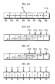
- This technique teaches a data processing apparatus that is a VLIW processor for executing 32-bit instructions that can simultaneously indicate a maximum of two operations.
- Figs. 1A and 1B show the instruction format of the stated technique, with Fig. 1A showing the instruction format for simultaneously indicating two operations and Fig. 1B showing the instruction format for indicating only one operation.
- This technique aims to improve code efficiency by including a 2-bit value in the format field 410 that shows the number of operations in each instruction and the execution order.
- a first embodiment of the present invention provides a VLIW processor that executes instructions of comparatively short word length, but which have a high degree of parallelism and a highly efficient code structure so that several operations can be simultaneously indicated. As one example, three or more operations can be indicated by a single 32-bit instruction.
- the first embodiment can be realized by a VLIW (Very Long Instruction Word) processor that decodes and executes an instruction that has at least two operation fields, of which a first operation field can only include one operation code for specifying an operation type and a second operation field includes a combination of one operation code and at least one operand used in an operation indicated by the second operation field
- the VLIW processor including: a first decoding unit for decoding the operation code in the first operation field; a first execution unit for executing an operation indicated by the operation code in the first operation field in accordance with a decoding result of the first decoding unit; a second decoding unit for decoding the operation code in the second operation field; and a second execution unit for executing the operation indicated by the operation code in the second operation field on data which is indicated by the operands in the second operation field, in accordance with a decoding result of the second decoding unit.
- VLIW Very Long Instruction Word
- a number of bits occupied by the operation code in the first operation field may be equal to a number of bits occupied by the operation code in the second operation field.
- the instruction may include three operation fields, wherein a third operation field in the three operation fields may occupy a same number of bits as the second operation field and may include a combination of one operation code and at least one operand, the VLIW processor further including: a third decoding unit which decodes, when an operation code is present in the third operation field, the operation code in the third operation field; and a third executing unit for executing an operation indicated by the operation code in the third operation field on data which is indicated by the operands in the third operation field, in accordance with a decoding result of the third decoding unit.
- VLIW processor with a high degree of parallelism whereby three operations can be simultaneously performed can be achieved.
- the first executing unit may control a control flow of a program including the instruction.
- the second executing unit may control transfer of the data that is indicated by the operands included in the second operation field
- the third executing unit may control executes an arithmetic logic operation on the data that is indicated by the operands included in the third operation field.
- VLIW processor decodes and executes an instruction that has at least two operation fields, of which a first operation field can only include one of (i) a single operation code for specifying an operation type and (ii) a constant, and a second operation field includes one of (i) a combination of one operation code and at least one operand used in an operation indicated by the second operation field and (ii) a constant
- the VLIW processor including: a first decoding unit which decodes, when an operation code is present in the first operation field, the operation code in the first operation field; a first executing unit for executing an operation indicated by the operation code in the first operation field, in accordance with a decoding result of the first decoding unit; a second decoding unit which decodes, when an operation code is present in the second operation field, the operation code in the second operation field; and a second
- the instruction also includes a format field including a format code indicating whether only a constant is located in the first operation field and whether only a constant is located in the second operation field
- the VLIW processor further including: a format decoding unit for decoding the format code; and a constant storage unit for extracting, when a decoding result of the format decoding unit shows that only a constant is present in at least one of the first operation field and the second operation field, the constant in the instruction and storing the extracted constant.
- constants placed in an operation field can be stored in the constant storage unit for use by an operation in a later instruction, so that decreases in code efficiency can be avoided even when handling constants of a comparatively long word length using instructions of a comparatively short word length.
- the format field, the first operation field, the operation code in the second operation field, each operand in the second operation field, the operation code in the third operation field, and each operand in the third operation field may each occupy n bits in the instruction.
- a VLIW processor may include: a fetch unit for fetching an L-bit instruction that includes n operation fields; and n operation units which are each associated with a different one of the n operation fields in the fetched instruction and each independently execute an operation indicated in the associated operation field in parallel with each other; the VLIW processor being characterized by the n operation fields not all being a same size, and by L not being an integer multiple of n .
- n may be 3 and L may be 32.
- the stated construction realizes a VLIW processor with a high degree of parallelism whereby three operations that are specified by a single 32-bit instruction can be simultaneously performed.
- a number of operands included in at least one operation field out of the n operation fields may be different to a number of operands in other operation fields in the n operation fields.
- the n operation fields may include at least one operation field composed of only an operation code and at least one operation field composed of an operation code and at least one operand.
- the instruction word length is shorter than the case when every operation field in an instruction contains a combination of an operation code and operands, so that a VLIW processor that executes instructions which have a highly efficient code construction can be realized.
- the present invention realizes a VLIW processor that executes instructions of comparatively short word length but which have a highly efficient code structure that allows several operations to be specified by a single instruction. This effect is especially noticeable for embedded processors that process multimedia data.
- the expression “instruction” refers to a set of code that is decoded and executed by the present processor simultaneously and in parallel
- the expression “operation” refers to a unit of processing, such as an arithmetic operation, a logic operation, a transfer, or a branch, which is executed by the present processor in parallel, as well as to the code which indicates each unit of processing.
- the present processor is a VLIW processor that decodes and executes instructions with a fixed word length of 32 bits.
- Fig. 2A shows the field structure of an instruction 50 to be executed by the present processor.
- Figs. 2B to 2D show sixteen instruction formats.
- the instruction formats in Fig. 2B simultaneously indicate three operations, the instruction formats in Fig. 2C two operations, and the instruction formats in Fig. 2D a single operation.
- This instruction 50 has a fixed word length of 32 bits and is composed of eight 4-bit physical fields shown in order starting from the MSB (Most Significant Bit) as P0.0 field 51, P1.0 field 52, ... P3.2 field 58 in Fig. 2A . Of these, the range from the P2.0 field 53 to the P2.2 field 55 is called the first operation field 59, while the range from the P3.0 field 56 to the P3.2 field 58 is called the second operation field 60.
- MSB Mobile Bit
- the legend "const” indicates a constant, and depending on the operation in which it is used, this can be a numeric constant or a character constant such as an immediate, an absolute address, or a displacement.
- the legend “op” represents an operation code that indicates an operation type, while the legend “Rs” indicates the register used as the source operand, “Rd” the register used as the destination operand, and "cc” an operation code indicating a branch operation that uses the stored value of a specialized 32-bit register provided in the present processor (the constant register 36 shown in Fig. 4 ) as the absolute address or relative address (displacement) of a branch destination.
- the constant "const” which is not appended with a number represents a constant to be stored in the specialized 32-bit register provided in the present processor (the constant register 36 shown in Fig. 4 ).
- the 4-bit constant "const" located in the P1.0 field 52 implies the constant that is to be stored in the constant register 36 which is implicitly indicated.
- Fig. 3 shows specific examples of the operations that can be indicated by the three kinds of operation code "cc", “op1", and “op2" given in Figs. 2B to 2D . These operations are described in detail below.
- the 4-bit operation code "cc" indicates one out of sixteen types of branch instruction.
- Each branch instruction is specified as a branch condition and a branch format.
- branch conditions include “equal to ('eq')", “not equal to ('neq')", and “greater than ('gt')”.
- the branch format can be a format where the stored value of the constant register 36 serves as the absolute address of the branch destination (denoted by having no "i" attached to the instruction mnemonic), or a format where the stored value of the constant register 36 serves as a relative address (denoted by having "i” attached to the instruction mnemonic).
- the operation code "eq” represents an operation that branches to a destination indicated through absolute addressing when a preceding comparison finds the compared values to be equal
- the operation code “eqi” represents an operation that branches to a destination indicated through relative addressing when a preceding comparison finds the compared values to be equal.
- the 4-bit operand “op1" can be used to indicate an arithmetic logic operation, such as any of an “add” (addition), a “sub” (subtraction), a “mul” (multiplication), an "and” (logical AND), or an “or” (logical OR), or an operation that is an inter-register transfer, such as any of a “mov” (transfer of word (32-bit) data), a “movh (transfer of halfword data), or a “movb” (transfer of one byte data).
- an arithmetic logic operation such as any of an “add” (addition), a “sub” (subtraction), a “mul” (multiplication), an "and” (logical AND), or an “or” (logical OR)
- an operation that is an inter-register transfer such as any of a “mov” (transfer of word (32-bit) data), a “movh (transfer of halfword data), or a “movb” (transfer of one byte data).
- the 4-bit operand "op2" can be used to indicate any of the arithmetic logic operations or inter-register transfers that can be indicated by the operand "op1", but can also be used to indicate a register-memory transfer operation such as an "ld” (load of one word data from memory into registers) or an “st” (store of one word data into memory from registers).
- the P0.0 field 51 holds a 4-bit format code that specifies the format of the instruction 50. More specifically, this P0.0 field 51 specifies one of the sixteen instruction formats shown in Figs. 2B to 2D .
- the P1.0 field 52 is a field holds a constant or an operation code for a branch operation.
- the first operation field 59 holds either a constant or a combination of (a) an operation code for indicating an operation (such as an arithmetic logic operation or inter-register transfer) that does not involve data transfer between the present processor and the periphery (memory), and (b) source and destination operands for the operation.
- the second operation field 60 can hold the same content as the first operation field 59 described above, but can also alternatively hold a combination of (a) an operation code for indicating an operation (such as memory-register transfer) that involves data transfer between the present processor and the periphery and (b) operands for the operation.
- a maximum of three operations can be indicated by a single instruction, and in this case, as can be seen from the triple operation formats shown in Fig. 2B , either of the following combinations of operation types can be used.
- the instructions of present processor have a highly efficient field structure that enables a maximum of three operations to be simultaneously indicated by a single 32-bit instruction.
- Fig. 4 is a block diagram showing the hardware construction of the processor of the present invention. As described above, this processor is a VLIW processor that can execute a maximum of three operations in parallel. The construction of the processor can be roughly divided into an instruction register 10, a decoder unit 20, and an execution unit 30.
- the instruction register 10 is a 32-bit register that stores one instruction that has been sent from the instruction fetch unit 39.
- the decoder unit 20 decodes the instruction held in the instruction register 10 and performs output on control lines to the execution unit 30 in accordance with the decoding result.
- This decoder unit 20 can itself be roughly divided into the format decoder 21 and the instruction decoder 22.
- the instruction decoder 22 is composed of a branch decoder 23 that decodes the "cc" operation code held in the P1.0 field 12 and controls the PC unit 33 accordingly, a first operation decoder 24 that decodes the operation code held in the P2.0 field i3 and controls the first operation unit 37 accordingly, and a second operation decoder 25 that decodes the operation code held in the P3.0 field 16 and controls the second operation unit 38 and operand access unit 40 accordingly.
- the format decoder 21 decodes the 4-bit format code held in the P0.0 field 11 to identify the instruction format of the instruction held in the instruction register 10 as one of the sixteen possible instruction formats shown in Figs. 2B to 2D .
- the format decoder 21 permits or prohibits decoding operations by the branch decoder 23, the first operation decoder 24, and the second operation decoder 25, and activates the register control unit 32 of the execution unit 30.
- the format decoder 21, the branch decoder 23, the first operation decoder 24, and the second operation decoder 25 fundamentally decode one operation in one cycle and send control signals to the execution unit 30.
- the 26-bit constant signal line 26 that connects the instruction register 10 with the execution unit 30 is a bus for transferring constants and operands located in the instruction register 10 to the execution unit 30.
- the execution unit 30 operates according to the decoding result of the decoder unit 20 and is a circuit that is capable of executing a maximum of three operations in parallel.
- This execution unit 30 is composed of an execution control unit 31, a PC unit 33, a register set 34, a first operation unit 37, a second operation unit 38, an instruction fetch unit 39, and an operand access unit 40.
- the constructions of the register control unit 32, the PC unit 33, and the constant register 36 are shown in greater detail in the other drawings.
- the execution control unit 31 refers in general to the control circuits and wiring for controlling the components numbered 33 to 40 in the execution unit 30 according to the decoding result of the decoder unit 20.
- This execution control unit 31 includes the components that are normally provided in a processor, such as circuits for timing control, operation permission/prohibition control, status management, and interruption control, as well as the constant register control unit 32 which is a characteristic component of the present processor.
- the constant register control unit 32 performs control so that a 4- or 16-bit constant "const" held in the instruction register 10 is stored in the constant register 36 based on indications given by the format decoder 21.
- the PC (Program Counter) unit 33 operates under the control of the branch decoder 23, and outputs the address in an external memory (not illustrated) of the next instruction to be decoded and executed to the instruction fetch unit 39.
- the instruction fetch unit 39 fetches an instruction block from the external memory (not illustrated) via a 32-bit IA (Instruction Address) bus and a 32-bit ID (Instruction Data) bus.
- the instruction fetch unit 39 stores the fetched instruction block in an internal instruction cache and supplies the instruction which corresponds to the address outputted by the PC unit 33 to the instruction register 10.
- the register set 34 is composed of fifteen 32-bit general registers 35 and one 32-bit constant register 36.
- the values which are stored in these sixteen registers 35 and 36 are transferred to the first operation unit 37 and the second operation unit 38 where an operation is performed or alternatively the values are allowed to pass, before being sent to the register set 34 or the operand access unit 40.
- the value stored in the constant register 36 can also be transferred to the PC unit 33, where it is used to generate an effective address that is used as a branch destination.
- the first operation unit 37 internally includes an ALU (Arithmetic Logic Unit) for performing arithmetic logic operations on two 32-bit sets of data and a multiplier for performing multiplications on two 32-bit sets of data.
- ALU Arimetic Logic Unit
- This first operation unit 37 is capable of executing two types of operation (namely, arithmetic logic operations, and inter-register transfer operations) under the control of the first operation decoder 24.
- the second operation unit 38 internally includes an ALU for performing arithmetic logic operations on two 32-bit sets of data and a multiplier for performing multiplications on two 32-bit sets of data, in the same way as the first operation unit 37.
- This second operation unit 38 is capable of executing two types of operation (namely, arithmetic logic operations, and inter-register transfer operations) under the control of the second operation decoder 25.
- the operand access unit 40 operates under the control of the second operation decoder 25 and is a circuit that transfers operands between the register set 34 and the external memory (not illustrated).
- the operand access unit 40 internally includes a buffer for storing operands and operand addresses.
- the operation code "ld" is in the P3.1 field 16 of the instruction register 10
- one word of data that is located in the external memory is loaded via the operand access unit 40 into one of the registers in the register set 34.
- the operation code "st" is present, meanwhile, the stored value of one of the registers in the register set 34 is stored in the external memory.
- the PC unit 33, the register set 34, the first operation unit 37, the second operation unit 38, and the operand access unit 40 are connected by internal buses (the L1 bus, the R1 bus, the L2 bus, the R2 bus, the D1 bus, and the D2 bus) as shown in Fig. 4 .
- the L1 bus and the R1 bus are each connected a respective one of the two input ports of the first operation unit 37
- the L2 bus and the R2 bus are each connected to a respective one of the two input ports of the second operation unit 38
- the D1 bus and the D2 bus are respectively connected to an output port of the first operation unit 37 and the second operation unit 38.
- Fig. 5 is a block diagram showing the detailed construction of the constant register 36 and of the peripheral circuits. Note here that the fixed value ("0") 27 in the drawings refers to fixed wiring for four signal lines carrying the constant "0".
- the constant register control unit 32 is composed of five 3-input selectors 32a-32e and three 4-input selectors 32f-32h, while the constant register 36 is composed of eight 4-bit registers 36a-36h.
- each set of input and output data is 4-bit parallel data.
- the constant register control unit 32 controls the eight input selectors 32a-32h so that a constant stored in the instruction register 10 or zeros are stored in the constant register 36 according to one of the four storage methods given below.
- Figs. 6A to 6D show the four possible storage methods in the present embodiment.
- Fig. 6A shows a storage method for when the format decoder 21 detects that the value stored in the P0.0 field 11 is "0" or "1". This equates to the case when only a 4-bit constant located in the P1.0 field 12 is stored in the constant register 36. More specifically, the data that is stored in the constant register 36 is shifted upwards (to the left in Fig. 6A ) in 4-bit units and the 4-bit constant stored in the P1.0 field 12 of the instruction register 10 is stored in the lowest-order 4-bit register 36h of the constant register 36.
- Fig. 6B shows a storage method for when the format decoder 21 detects that the value stored in the P0.0 field 11 is "4". This equates to the case when a 16-bit constant located between the P1.0 field 12 and the P2.2 field 15 is stored in the constant register 36. More specifically, the data that is stored in the lower 16 bits 36e-36h of the constant register 36 is shifted to the upper 16 bits 36a-36d and the 16-bit constant located between the P1.0 field 12 and the P2.2 field 15 of the instruction register 10 is stored in the lowest-order 16-bits 36e-36h of the constant register 36.
- Fig. 6C shows a storage method for when the format decoder 21 detects that the value stored in the P0.0 field 11 is "5". This equates to the case when a 16-bit constant located in the P1.0 field 12 and between the P3.0 field 16 and the P3.2 field 18 is stored in the constant register 36. More specifically, the data that is stored in the lower 16 bits 36e-36h of the constant register 36 is shifted to the upper 16 bits 36a-36d and the 16-bit constant located in the P1.0 field 12 and between the P3.0 field 16 and the P3.2 field 18 of the instruction register 10 is stored in the lowest-order 16-bits 36e-36h of the constant register 36.
- Fig. 6D shows a storage method for when the format decoder 21 detects that the value stored in the P0.0 field 11 is "2", “3", or "A”, or when the instruction decoder 22 detects that the constant register (R15) is indicated by at least one of the P2.1 field 14, the P2.2 field 15, the P3.2 field 17, and the P3.3 field 18.
- This equates to the case where the value stored in the constant register 36 is reset to all zeros (which is to say, the constant register 36 is cleared), after the stored value of the constant register 36 has been used by at least one of a branch operation located in the P1.0 field 12, an operation in the first operation field 59 or an operation in the second operation field 60. More specifically, immediately after the stored value of the constant register 36 has been read out to one of the PC unit 33, the first operation unit 37 or the second operation unit 38, a 32-bit constant with the value "0" is written into the constant register 36.
- a zero extension refers to the insertion of zeros that is performed when the effective number of bits of a value is below a predetermined number of bits, with zeros being inserted into the higher bit positions so that the value takes up the predetermined number of bits.
- the constant that is already stored in the constant register 36 is shifted and a new value is stored. Also, after the value stored in the constant register 36 is read out and used, this stored value is deleted. By doing so, the constant register 36 is able to successively accumulate constants until the next time its stored content is used.
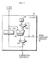
- Fig. 7 is a block diagram showing the construction of the PC unit 33 in detail.
- the PC unit 33 is composed of a fixed value ("4") 33a, that is wiring which permanently carries the constant "4", a 2-input selector 33b, an adder 33c, a PC (Program Counter) 33d for storing an address of the next instruction to be decoded and executed, and a 4-input selector 33e.
- the selectors 33b and 33e operate in accordance with control signals from the decoder unit 20, so that the selector 33e outputs one of the following three types of values to the instruction fetch unit 39 as the effective address.
- the PC unit 33 includes a specialized adder 33c, and is constructed to directly use the value stored by the constant register 36, so that branch execution control can be performed with the stored value of the constant register 36 as a relative address or an absolute address in parallel with and independent of the operations performed by the first operation unit 37 and the second operation unit 38.
- Fig. 8 is a flowchart showing an example of a procedure that handles 32-bit constants.
- step S80 the difference between the stored values of the registers R0 and R1 is found (step S80), and the result is multiplied by the stored value of R2 (step S81).
- step S81 the 32-bit constant "0x87654321" (the value "87654321” in hexadecimal) is then added to the result of this (steps S82, S83), and finally the register R0 is cleared (step S84).
- Fig. 9 shows an example of a program that has the present processor perform the procedure shown in Fig. 8 .
- the program is composed of the three instructions 71-73.
- one line corresponds to one instruction, and the content of each instruction is shown by mnemonics located in the separate fields of each instruction.
- the value of each constant is expressed in hexadecimal.
- Fig. 10 is a timing chart showing the operation of the present processor when executing the program shown in Fig. 9 .
- This Fig. 10 shows the clock cycles, the content of the general registers R0-R3 and the register R15, and the data that flows on the four buses L1, R1, L2, and R2.
- the present processor After the instruction 71 has been loaded into the instruction register 10, the present processor performs the operations shown in the clock cycles t0-t1 in Fig. 10 .
- the format decoder 21 judges from the value "fmt4" of the P0.0 field 11 in the instruction register 10 that the present instruction is a twin operation instruction with the format code "4", and so controls the execution unit 30 so that the two operations described below are executed in parallel.
- the constant register control unit 32 controls its eight internal selectors 32a-32h so that the 16-bit constant (0x8765) located between the P1.0 field 12 to the P2.2 field 15 is stored in the lower 16 bits of the constant register 36 according to the storage method shown in Fig. 6B . Accordingly, the content of the register R15 changes from "0x00000000” to "0x00008765” as shown in the clock cycles t0-t1 in Fig. 10 .
- the second operation unit 38 receives an input of the stored value "0x33333333” of the general register R0 and the stored value "0x22222222” of the general register R1, and after subtracting the latter from the former, stores the result in the general register R0.
- the stored content of the general register R0 changes from the value "0x33333333” to the value "0x11111111” in the clock cycles t0-t1 shown in Fig. 10 .
- the present processor operates as shown in clock cycles t1-t2 in Fig. 10 .
- the format decoder 21 judges from the value "fmt4" of the P0.0 field 11 in the instruction register 10 that the present instruction is a twin operation instruction with the format code "4", and so controls the execution unit 30 so that the two operations described below are executed in parallel.
- the constant register control unit 32 controls its eight internal selectors 32a-32h so that the 16-bit constant (0x4321) located between the P1.0 field 12 to the P2.2 field 15 is stored in the lower 16 bits of the constant register 36 according to the storage method shown in Fig. 6B . Accordingly, the content of the register R15 changes from "0x00008765” to "0x87654321" as shown in the clock cycles t1-t2 in Fig. 10 .
- the second operation unit 38 receives an input of the stored value "0x00000004" of the general register R2 and the stored value "0x11111111” of the general register R0, and multiplies the two together before storing the result in the general register R0.
- the stored content of the general register R0 changes from the value "0x11111111” to the value "0x44444444" in the clock cycles t1-t2 shown in Fig. 10 .
- the present processor operates as shown in clock cycles t2-t3 in Fig. 10 .
- the format decoder 21 judges from the value "fmt7" of the P0.0 field 11 in the instruction register 10 that the present instruction is a twin operation instruction with the format code "7”, and so controls the execution unit 30 so that the two operations described below are executed in parallel.
- the first operation unit 37 receives an input of the stored value "0x87654321" of the general register R15 and the stored value "0x44444444” of the general register R0, and adds the two together before storing the result in the general register R0.
- the stored content of the general register R0 changes from the value "0x44444444” to the value "0xCBA98765" in the clock cycles t2-t3 shown in Fig. 10 .
- the second operation unit 38 receives an input of the 8-bit constant ("0x00") that is located in the P1.0 field 12 and the P3.1 field 17 and allows this constant to pass so that it is stored in the general register R3.
- the content of the general register R3 changes from the previously held value "0xFEDCBA98" to "0x00000000", as shown for the clock cycles t2-t3 in Fig. 10 .
- the 32-bit constant "0x87654321" is split into two parts that are arranged into the two instructions 71 and 72, with these parts being successively stored in the constant register 36 by shifting its stored value.
- This stored constant is then used according to the third instruction, instruction 73.
- the procedure shown in the flowchart of Fig. 8 can be executed by the three instructions 71-73.
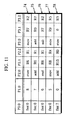
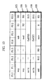
- Fig. 11 shows an example of a program that handles a 16 bit constant. This program is composed of the five instructions 74 to 78.
- the format decoder 21 judges from the value "fmt0" of the P0.0 field 11 in the instruction register 10 that the present instruction is a triple operation instruction with the format code "0", and so controls the execution unit 30 so that the three operations described below are executed in parallel.
- the constant register control unit 32 controls its eight internal selectors 32a-32h so that the 4-bit constant ("0x8") located in the P1.0 field 12 is stored in the lowest 4 bits of the constant register 36 according to the storage method shown in Fig. 6A .
- the first operation unit 37 receives an input of the stored value of the general register R6, and allows this value to pass so that it is stored in the general register R1.
- the second operation unit 38 receives an input of the stored value of the general register R7, and allows this value to pass so that it is stored in the general register R2.
- the format decoder 21 judges from the value "fmt0" of the P0.0 field 11 in the instruction register 10 that the present instruction is a triple operation instruction with the format code "0", and so controls the execution unit 30 so that the three operations described below are executed in parallel.
- the constant register control unit 32 controls its eight internal selectors 32a-32h so that the 4-bit constant ("0x7") located in the P1.0 field 12 is stored in the lowest 4 bits of the constant register 36 according to the storage method shown in Fig. 6A . After this operation, the constant "0x87" is set in the lowest 8 bits of the constant register 36.
- the first operation unit 37 receives an input of the stored values of the general register R0 and the general register R1, and adds these values together.
- the first operation unit 37 stores the addition result in the general register R1.
- the second operation unit 38 receives an input of the stored values of the general register R0 and the general register R2, and adds these values together.
- the second operation unit 38 stores the addition result in the general register R2.
- Instructions 76 and 77 are executed in the same way as described above, and as a result the constant "0x8765" is stored in the lower 16 bits of the constant register 36.
- the present processor operates in the same way as when processing instruction 73.
- the 16-bit constant "0x8765” is split into four parts that are arranged into the instructions 74-77, with these parts being successively stored in the constant register 36 by shifting its stored value. This stored constant is then used according to the fifth instruction, instruction 78.
- standard processor refers to a processor that executes instructions whose word length is fixed at 32 bits, and is the same as the present processor, except for the lack of a construction, such as the constant register 36 and the constant register control unit 32, for accumulating constants that have been divided between instructions.
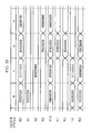
- Fig. 12A shows the field definition of the instructions that are executed by a standard processor
- Fig. 12B shows the format of the instructions.
- the standard processor can execute three types of twin operation instruction, instructions 101-103, and one type of single operation instruction, instruction 104.
- Fig. 13 shows an example of a program to be executed by the standard processor. This program has the same processing content as the program shown in Fig. 9 , which is to say the same procedure as the flowchart shown in Fig. 8 .
- the program for the standard processor includes two more instructions that the program for the processor of the present invention.
- the reason the "NOP codes" are included in the instructions 105 and 106 is that the instruction 106 uses the operation result of'the instruction 105, so that these instructions cannot be executed in parallel. Also, the reason the constant "0x87654321" is divided into an upper 16 bits and a lower 16 bits that are set in the constant register Ri (instructions 107 and 108) is that it is not possible to set a 32-bit constant and an operation code for a setting instruction in a single 32-bit instruction.
- Fig. 14 also shows an example of a program for a standard processor. This program has the same processing content as program shown in Fig. 11 . As can be seen by comparing Fig. 14 and Fig. 11 , the program for the standard processor includes one more instruction than the program for the processor of the present invention.
- the instructions executed by the processor of the present invention have a highly efficient field structure whereby a maximum of three operations can be indicated using a comparatively short word length of 32 bits.
- a 16-bit or 32-bit constant that has been divided across a plurality of instructions can be accumulated in the constant register 36 to restore the constant to its original form, with it then being used for a branch operation or arithmetic logic operation. Accordingly, when a small region is available in an instruction, this region can be effectively used for locating a part of a constant, so that the code size of the program can be reduced compared with when the same processing is performed by a standard processor.
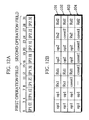
- Figs. 15A to 15D show the instruction formats of VLIW processors that are modifications of the present invention.
- the smallest interval demarcated by the vertical lines represents one bit, while the legend "fmt" shows the format field.
- the instruction shown in Fig. 15A is composed of a 5-bit format field, a 7-bit operation field, and two 10-bit operation fields.
- the instruction shown in Fig. 15B meanwhile, is composed of a 2-bit format field, a 4-bit operation field, and two 13-bit operation fields.
- the instruction shown in Fig. 15C is composed of a 3-bit format field, a 3-bit operation field, and two 13-bit operation fields.
- the instruction shown in Fig. 15D is composed of a 4-bit format field, a 2-bit operation field, and two 13-bit operation fields.
- the four types of instructions described above also have the following characteristics which differ from those of the instruction 50 described in the above embodiment.
- the instruction shown in Fig. 15A has the advantages of an enlarged format field, meaning a greater number of instruction types can be defined, and of the ability to provide at least one operand in each of the three operation fields.
- the instructions shown in Fig. 15B to Fig. 15D meanwhile, have the advantage of two enlarged operation codes ("op2" and "op3"), so that a greater variety of operations can be defined.
- Fig. 16 is a block diagram showing the construction of a VLIW processor of the present invention for executing the instruction shown in Fig. 15A .
- the fundamental construction of the processor is the same, although there are some differences in the connections between the instruction registers 10, 110 and the decoder units 20, 120.
- VLIW processors for executing the modified instructions shown in Figs. 15A to 15D can be realized by making only partial changes to the VLIW processor described in the above embodiment.
- a VLIW processor comprising fetch means for fetching an L-bit instruction that includes n operation fields; and n operation units which are each associated with a different one of the n operation fields in the fetched instruction and each independently execute an operation indicated in the associated operation field in parallel with each other; the VLIW processor being characterised by the n operation fields not all being a same size, and by L not being an integer multiple of n .
- At least one of the n operation fields has a different length to other operation fields in the n operation fields.
- n is 3 and L is 32.
- a number of operands included in at least one operation field out of the n operation fields is different to a number of operands in other operation fields in the n operation fields.
- n is 3 and L is 32.
- the n operation fields include at least one operation field composed of an operation code with no operand and at least one operation field composed of an operation code and at least one operand.
- n is 3 and L is 32.
Claims (4)
- VLIW-Prozessor, umfassend:Abrufmittel (39) zum Abrufen einer Anweisung, die eine Vielzahl von Operationsfeldern (52, 59) enthält; undeine Decodereinheit (20) zum Decodieren der Vielzahl von Operationsfeldern (52, 59) in der abgerufenen Anweisung parallel miteinander;wobei der VLIW-Prozessor dadurch gekennzeichnet ist, dass:die Vielzahl von Operationsfeldern einen ersten Typ von Operationsfeld (52) und einen zweiten Typ von Operationsfeld (59 oder 60) enthält,der erste Typ von Operationsfeld (52) an einer ersten im Voraus bestimmten Position in der Anweisung angeordnet ist und aus einem Operationscode mit keinem Operanden davon zusammengesetzt ist,der zweite Typ von Operationsfeld (59 oder 60) an einer zweiten im Voraus bestimmten Position in der Anweisung angeordnet ist und aus einem Operationscode und einem oder mehreren Operanden zusammengesetzt ist, unddie Decodereinheit (20) enthält:einen ersten Decoder (23) zum Decodieren des Operationscodes in dem ersten Typ von Operationsfeld (52), undeinen zweiten Decoder (24 oder 25) zum Decodieren des Operationscodes in dem zweiten Typ von Operationsfeld (59 oder 60).
- VLIW-Prozessor nach Anspruch 1, weiter umfassend
eine Ausführungseinheit (30), die enthält:eine Ausführungssteuereinheit (31) zum Durchführen einer Steuerung gemäß einem decodierten Ergebnis des ersten Decoders (23), undeine Rechenoperationseinheit (37 und 38) zum Durchführen einer Rechenoperation gemäß einem decodierten Ergebnis des zweiten Decoders (24 und 25) unter Verwendung eines Operanden. - VLIW-Prozessor nach Anspruch 1 oder 2,
wobei die Vielzahl von Operationsfeldern aus einem Operationsfeld des ersten Typs von Operationsfeld und zwei Operationsfeldern des zweiten Typs von Operationsfeld zusammengesetzt ist, und
die Decodereinheit (20) weiter einen dritten Decoder (25) zusätzlich zu dem ersten Decoder (23) und dem zweiten Decoder (24) enthält,
wobei der zweite Decoder (24) und der dritte Decoder (25) jeder ein jeweiliges eines der beiden Operationsfelder des zweiten Typs von Operationsfeld decodieren. - VLIW-Prozessor nach einem der vorstehenden Ansprüche, wobei der Operationscode in dem ersten Typ von Operationsfeld (52) ein Bedingungscode-Operationscode ist.
Applications Claiming Priority (3)
| Application Number | Priority Date | Filing Date | Title |
|---|---|---|---|
| JP15904897A JP3790607B2 (ja) | 1997-06-16 | 1997-06-16 | Vliwプロセッサ |
| EP06076804.1A EP1734440B1 (de) | 1997-06-16 | 1998-06-15 | Prozessor zur Ausführung von hochwirksamen VLIW-Befehlen |
| EP98304690A EP0886210B1 (de) | 1997-06-16 | 1998-06-15 | Prozessor zur Ausführung von hochwirksamen VLIW-Befehlen |
Related Parent Applications (4)
| Application Number | Title | Priority Date | Filing Date |
|---|---|---|---|
| EP98304690.5 Division | 1998-06-15 | ||
| EP06076804.1A Division-Into EP1734440B1 (de) | 1997-06-16 | 1998-06-15 | Prozessor zur Ausführung von hochwirksamen VLIW-Befehlen |
| EP06076804.1A Division EP1734440B1 (de) | 1997-06-16 | 1998-06-15 | Prozessor zur Ausführung von hochwirksamen VLIW-Befehlen |
| EP06076804.1 Division | 2006-09-29 |
Publications (2)
| Publication Number | Publication Date |
|---|---|
| EP2138932A1 EP2138932A1 (de) | 2009-12-30 |
| EP2138932B1 true EP2138932B1 (de) | 2012-02-29 |
Family
ID=15685098
Family Applications (4)
| Application Number | Title | Priority Date | Filing Date |
|---|---|---|---|
| EP06076804.1A Expired - Lifetime EP1734440B1 (de) | 1997-06-16 | 1998-06-15 | Prozessor zur Ausführung von hochwirksamen VLIW-Befehlen |
| EP98304690A Expired - Lifetime EP0886210B1 (de) | 1997-06-16 | 1998-06-15 | Prozessor zur Ausführung von hochwirksamen VLIW-Befehlen |
| EP09172121A Expired - Lifetime EP2138932B1 (de) | 1997-06-16 | 1998-06-15 | Prozessor zur Ausführung von hochwirksamen VLIW-Befehlen |
| EP09172123A Withdrawn EP2138933A1 (de) | 1997-06-16 | 1998-06-15 | Prozessor zur Ausführung von hochwirksamen VLIW-Befehlen |
Family Applications Before (2)
| Application Number | Title | Priority Date | Filing Date |
|---|---|---|---|
| EP06076804.1A Expired - Lifetime EP1734440B1 (de) | 1997-06-16 | 1998-06-15 | Prozessor zur Ausführung von hochwirksamen VLIW-Befehlen |
| EP98304690A Expired - Lifetime EP0886210B1 (de) | 1997-06-16 | 1998-06-15 | Prozessor zur Ausführung von hochwirksamen VLIW-Befehlen |
Family Applications After (1)
| Application Number | Title | Priority Date | Filing Date |
|---|---|---|---|
| EP09172123A Withdrawn EP2138933A1 (de) | 1997-06-16 | 1998-06-15 | Prozessor zur Ausführung von hochwirksamen VLIW-Befehlen |
Country Status (10)
| Country | Link |
|---|---|
| US (7) | US6085306A (de) |
| EP (4) | EP1734440B1 (de) |
| JP (1) | JP3790607B2 (de) |
| KR (1) | KR100534967B1 (de) |
| CN (2) | CN1178145C (de) |
| DE (1) | DE69838966T2 (de) |
| IL (1) | IL124904A (de) |
| MY (2) | MY116751A (de) |
| SG (3) | SG111062A1 (de) |
| TW (1) | TW490636B (de) |
Families Citing this family (56)
| Publication number | Priority date | Publication date | Assignee | Title |
|---|---|---|---|---|
| JP3790607B2 (ja) * | 1997-06-16 | 2006-06-28 | 松下電器産業株式会社 | Vliwプロセッサ |
| JP3412462B2 (ja) * | 1997-07-30 | 2003-06-03 | 松下電器産業株式会社 | プロセッサ |
| US6219776B1 (en) * | 1998-03-10 | 2001-04-17 | Billions Of Operations Per Second | Merged array controller and processing element |
| EP0953898A3 (de) * | 1998-04-28 | 2003-03-26 | Matsushita Electric Industrial Co., Ltd. | Prozessor zur Ausführung von Befehlen aus dem Speicher mittels eines Programmzählers und Kompiler, Assembler, Programmverbinder und Fehlerbeseitiger für einen solchen Prozessor |
| JP2001034471A (ja) | 1999-07-19 | 2001-02-09 | Mitsubishi Electric Corp | Vliw方式プロセッサ |
| AU6864400A (en) * | 1999-08-30 | 2001-03-26 | Ip Flex Inc. | Control unit and recorded medium |
| JP3730455B2 (ja) * | 1999-10-01 | 2006-01-05 | 富士通株式会社 | 情報処理装置及び情報処理方法 |
| US20020004897A1 (en) * | 2000-07-05 | 2002-01-10 | Min-Cheng Kao | Data processing apparatus for executing multiple instruction sets |
| US20030023830A1 (en) * | 2001-07-25 | 2003-01-30 | Hogenauer Eugene B. | Method and system for encoding instructions for a VLIW that reduces instruction memory requirements |
| EP1530754A1 (de) * | 2002-08-05 | 2005-05-18 | Koninklijke Philips Electronics N.V. | Prozessor und verfahren zur ausführung von vliw-befehlen |
| EP1530755B1 (de) * | 2002-08-16 | 2019-11-06 | Intel Corporation | Vorrichtung, verfahren und compiler zum ermöglichen der verarbeitung von befehlen mit variablen längen in einem prozessor mit sehr langem befehlswort |
| AU2003253159A1 (en) | 2002-09-24 | 2004-04-19 | Koninklijke Philips Electronics N.V. | Apparatus, method ,and compiler enabling processing of load immediate instructions in a very long instruction word processor |
| US8364935B2 (en) * | 2002-10-11 | 2013-01-29 | Nytell Software LLC | Data processing apparatus address range dependent parallelization of instructions |
| US8211338B2 (en) | 2003-07-01 | 2012-07-03 | Transitions Optical, Inc | Photochromic compounds |
| JP4283131B2 (ja) * | 2004-02-12 | 2009-06-24 | パナソニック株式会社 | プロセッサ及びコンパイル方法 |
| US8687010B1 (en) | 2004-05-14 | 2014-04-01 | Nvidia Corporation | Arbitrary size texture palettes for use in graphics systems |
| US8736628B1 (en) | 2004-05-14 | 2014-05-27 | Nvidia Corporation | Single thread graphics processing system and method |
| US8736620B2 (en) * | 2004-05-14 | 2014-05-27 | Nvidia Corporation | Kill bit graphics processing system and method |
| US8860722B2 (en) * | 2004-05-14 | 2014-10-14 | Nvidia Corporation | Early Z scoreboard tracking system and method |
| US8743142B1 (en) | 2004-05-14 | 2014-06-03 | Nvidia Corporation | Unified data fetch graphics processing system and method |
| US7146491B2 (en) * | 2004-10-26 | 2006-12-05 | Arm Limited | Apparatus and method for generating constant values |
| KR100636596B1 (ko) | 2004-11-25 | 2006-10-23 | 한국전자통신연구원 | 고에너지 효율 병렬 처리 데이터 패스 구조 |
| US7523295B2 (en) * | 2005-03-21 | 2009-04-21 | Qualcomm Incorporated | Processor and method of grouping and executing dependent instructions in a packet |
| US7849466B2 (en) * | 2005-07-12 | 2010-12-07 | Qualcomm Incorporated | Controlling execution mode of program threads by applying a mask to a control register in a multi-threaded processor |
| JP4916151B2 (ja) * | 2005-09-29 | 2012-04-11 | ルネサスエレクトロニクス株式会社 | 並列演算装置 |
| WO2007145319A1 (ja) * | 2006-06-15 | 2007-12-21 | Nec Corporation | プロセッサ、および、命令制御方法 |
| US8537168B1 (en) | 2006-11-02 | 2013-09-17 | Nvidia Corporation | Method and system for deferred coverage mask generation in a raster stage |
| US8314803B2 (en) | 2007-08-15 | 2012-11-20 | Nvidia Corporation | Buffering deserialized pixel data in a graphics processor unit pipeline |
| US8599208B2 (en) * | 2007-08-15 | 2013-12-03 | Nvidia Corporation | Shared readable and writeable global values in a graphics processor unit pipeline |
| US8521800B1 (en) | 2007-08-15 | 2013-08-27 | Nvidia Corporation | Interconnected arithmetic logic units |
| US9183607B1 (en) | 2007-08-15 | 2015-11-10 | Nvidia Corporation | Scoreboard cache coherence in a graphics pipeline |
| US20090046105A1 (en) * | 2007-08-15 | 2009-02-19 | Bergland Tyson J | Conditional execute bit in a graphics processor unit pipeline |
| US8736624B1 (en) | 2007-08-15 | 2014-05-27 | Nvidia Corporation | Conditional execution flag in graphics applications |
| US8775777B2 (en) * | 2007-08-15 | 2014-07-08 | Nvidia Corporation | Techniques for sourcing immediate values from a VLIW |
| US9280480B2 (en) | 2008-01-11 | 2016-03-08 | International Business Machines Corporation | Extract target cache attribute facility and instruction therefor |
| US7895419B2 (en) | 2008-01-11 | 2011-02-22 | International Business Machines Corporation | Rotate then operate on selected bits facility and instructions therefore |
| US7870339B2 (en) | 2008-01-11 | 2011-01-11 | International Business Machines Corporation | Extract cache attribute facility and instruction therefore |
| US7734900B2 (en) | 2008-01-11 | 2010-06-08 | International Business Machines Corporation | Computer configuration virtual topology discovery and instruction therefore |
| US7739434B2 (en) * | 2008-01-11 | 2010-06-15 | International Business Machines Corporation | Performing a configuration virtual topology change and instruction therefore |
| US20100004542A1 (en) | 2008-07-03 | 2010-01-07 | Texas Instruments Incorporated | System and method for ultrasound color doppler imaging |
| US8418268B2 (en) * | 2009-12-04 | 2013-04-16 | Global Trademarks, Llc | Garment having support |
| US9678754B2 (en) * | 2010-03-03 | 2017-06-13 | Qualcomm Incorporated | System and method of processing hierarchical very long instruction packets |
| US8228109B2 (en) | 2010-06-28 | 2012-07-24 | Freescale Semiconductor, Inc. | Transmission gate circuitry for high voltage terminal |
| US8804764B2 (en) | 2010-12-21 | 2014-08-12 | International Business Machines Corporation | Data path for data extraction from streaming data |
| US20120198213A1 (en) * | 2011-01-31 | 2012-08-02 | International Business Machines Corporation | Packet handler including plurality of parallel action machines |
| JP5813484B2 (ja) * | 2011-11-30 | 2015-11-17 | ルネサスエレクトロニクス株式会社 | Vliwプロセッサと命令構造と命令実行方法 |
| US9411595B2 (en) | 2012-05-31 | 2016-08-09 | Nvidia Corporation | Multi-threaded transactional memory coherence |
| US9824009B2 (en) | 2012-12-21 | 2017-11-21 | Nvidia Corporation | Information coherency maintenance systems and methods |
| US10102142B2 (en) | 2012-12-26 | 2018-10-16 | Nvidia Corporation | Virtual address based memory reordering |
| US9317251B2 (en) | 2012-12-31 | 2016-04-19 | Nvidia Corporation | Efficient correction of normalizer shift amount errors in fused multiply add operations |
| US9886277B2 (en) | 2013-03-15 | 2018-02-06 | Intel Corporation | Methods and apparatus for fusing instructions to provide OR-test and AND-test functionality on multiple test sources |
| US9483266B2 (en) | 2013-03-15 | 2016-11-01 | Intel Corporation | Fusible instructions and logic to provide OR-test and AND-test functionality using multiple test sources |
| US9569385B2 (en) | 2013-09-09 | 2017-02-14 | Nvidia Corporation | Memory transaction ordering |
| WO2016064636A1 (en) * | 2014-10-23 | 2016-04-28 | Talon Technologies, Inc. | Garment with multilayer internal abdominal support panels |
| CN106160717B (zh) | 2015-04-03 | 2020-08-18 | 恩智浦美国有限公司 | 传输门电路 |
| TWI707272B (zh) * | 2019-04-10 | 2020-10-11 | 瑞昱半導體股份有限公司 | 可執行指令的電子裝置以及指令執行方法 |
Family Cites Families (67)
| Publication number | Priority date | Publication date | Assignee | Title |
|---|---|---|---|---|
| US4295193A (en) * | 1979-06-29 | 1981-10-13 | International Business Machines Corporation | Machine for multiple instruction execution |
| US5050070A (en) * | 1988-02-29 | 1991-09-17 | Convex Computer Corporation | Multi-processor computer system having self-allocating processors |
| US5202967A (en) * | 1988-08-09 | 1993-04-13 | Matsushita Electric Industrial Co., Ltd. | Data processing apparatus for performing parallel decoding and parallel execution of a variable word length instruction |
| US5000000A (en) * | 1988-08-31 | 1991-03-19 | University Of Florida | Ethanol production by Escherichia coli strains co-expressing Zymomonas PDC and ADH genes |
| US5615349A (en) | 1990-09-04 | 1997-03-25 | Mitsubishi Denki Kabushiki Kaisha | Data processing system capable of execution of plural instructions in parallel |
| JP2835103B2 (ja) * | 1989-11-01 | 1998-12-14 | 富士通株式会社 | 命令指定方法及び命令実行方式 |
| JPH04143819A (ja) * | 1989-12-15 | 1992-05-18 | Hitachi Ltd | 消費電力制御方法、半導体集積回路装置およびマイクロプロセツサ |
| DE4040382C2 (de) * | 1989-12-15 | 1999-03-11 | Hitachi Ltd | Integrierte Halbleiterschaltungsanordnung mit niederer Leistungsaufnahme und Verfahren zu ihrem Betrieb |
| US5333280A (en) * | 1990-04-06 | 1994-07-26 | Nec Corporation | Parallel pipelined instruction processing system for very long instruction word |
| DE69130723T2 (de) * | 1990-10-05 | 1999-07-22 | Koninkl Philips Electronics Nv | Verarbeitungsgerät mit Speicherschaltung und eine Gruppe von Funktionseinheiten |
| JP2908598B2 (ja) * | 1991-06-06 | 1999-06-21 | 松下電器産業株式会社 | 情報処理装置 |
| JP3186095B2 (ja) | 1991-07-05 | 2001-07-11 | 日本電気株式会社 | 演算処理装置 |
| JPH0527970A (ja) * | 1991-07-18 | 1993-02-05 | Seikosha Co Ltd | 演算装置 |
| JP2848727B2 (ja) | 1991-11-18 | 1999-01-20 | 株式会社東芝 | 並列演算処理装置 |
| DE69325826T2 (de) * | 1992-01-06 | 2000-02-24 | Hitachi Ltd | Rechner mit einer Parallelverarbeitungsfähigkeit |
| JPH05233281A (ja) * | 1992-02-21 | 1993-09-10 | Toshiba Corp | 電子計算機 |
| US5371864A (en) * | 1992-04-09 | 1994-12-06 | International Business Machines Corporation | Apparatus for concurrent multiple instruction decode in variable length instruction set computer |
| US5617549A (en) * | 1992-10-06 | 1997-04-01 | Hewlett-Packard Co | System and method for selecting and buffering even and odd instructions for simultaneous execution in a computer |
| US6002880A (en) * | 1992-12-29 | 1999-12-14 | Philips Electronics North America Corporation | VLIW processor with less instruction issue slots than functional units |
| US5485629A (en) * | 1993-01-22 | 1996-01-16 | Intel Corporation | Method and apparatus for executing control flow instructions in a control flow pipeline in parallel with arithmetic instructions being executed in arithmetic pipelines |
| US5384722A (en) * | 1993-03-10 | 1995-01-24 | Intel Corporation | Apparatus and method for determining the Manhattan distance between two points |
| JP2636136B2 (ja) | 1993-04-27 | 1997-07-30 | 工業技術院長 | 演算処理装置及び演算処理方法 |
| EP0950946B1 (de) | 1993-11-05 | 2001-08-16 | Intergraph Corporation | Superskalare Rechnerarchitektur mit Softwarescheduling |
| JP3199205B2 (ja) * | 1993-11-19 | 2001-08-13 | 株式会社日立製作所 | 並列演算装置 |
| GB9412435D0 (en) * | 1994-06-21 | 1994-08-10 | Inmos Ltd | Computer instruction addressing |
| US6334219B1 (en) * | 1994-09-26 | 2001-12-25 | Adc Telecommunications Inc. | Channel selection for a hybrid fiber coax network |
| ZA9510127B (en) * | 1994-12-01 | 1996-06-06 | Intel Corp | Novel processor having shift operations |
| WO1996029646A1 (fr) * | 1995-03-17 | 1996-09-26 | Hitachi, Ltd. | Processeur |
| US5669001A (en) * | 1995-03-23 | 1997-09-16 | International Business Machines Corporation | Object code compatible representation of very long instruction word programs |
| US5774726A (en) * | 1995-04-24 | 1998-06-30 | Sun Microsystems, Inc. | System for controlled generation of assembly language instructions using assembly language data types including instruction types in a computer language as input to compiler |
| JP2931890B2 (ja) * | 1995-07-12 | 1999-08-09 | 三菱電機株式会社 | データ処理装置 |
| US5848288A (en) | 1995-09-20 | 1998-12-08 | Intel Corporation | Method and apparatus for accommodating different issue width implementations of VLIW architectures |
| US5884323A (en) * | 1995-10-13 | 1999-03-16 | 3Com Corporation | Extendible method and apparatus for synchronizing files on two different computer systems |
| US5774737A (en) * | 1995-10-13 | 1998-06-30 | Matsushita Electric Industrial Co., Ltd. | Variable word length very long instruction word instruction processor with word length register or instruction number register |
| US5822606A (en) * | 1996-01-11 | 1998-10-13 | Morton; Steven G. | DSP having a plurality of like processors controlled in parallel by an instruction word, and a control processor also controlled by the instruction word |
| US5852741A (en) | 1996-05-15 | 1998-12-22 | Philips Electronics North America Corporation | VLIW processor which processes compressed instruction format |
| US5826054A (en) | 1996-05-15 | 1998-10-20 | Philips Electronics North America Corporation | Compressed Instruction format for use in a VLIW processor |
| US5787302A (en) * | 1996-05-15 | 1998-07-28 | Philips Electronic North America Corporation | Software for producing instructions in a compressed format for a VLIW processor |
| US5748936A (en) * | 1996-05-30 | 1998-05-05 | Hewlett-Packard Company | Method and system for supporting speculative execution using a speculative look-aside table |
| JP3442225B2 (ja) * | 1996-07-11 | 2003-09-02 | 株式会社日立製作所 | 演算処理装置 |
| JP3745039B2 (ja) * | 1996-08-01 | 2006-02-15 | 株式会社ルネサステクノロジ | 遅延命令を有するマイクロプロセッサ |
| JPH10232779A (ja) | 1997-01-24 | 1998-09-02 | Texas Instr Inc <Ti> | 命令並列処理方法及び装置 |
| US5805850A (en) * | 1997-01-30 | 1998-09-08 | International Business Machines Corporation | Very long instruction word (VLIW) computer having efficient instruction code format |
| JP3578883B2 (ja) * | 1997-01-31 | 2004-10-20 | 三菱電機株式会社 | データ処理装置 |
| US5881307A (en) * | 1997-02-24 | 1999-03-09 | Samsung Electronics Co., Ltd. | Deferred store data read with simple anti-dependency pipeline inter-lock control in superscalar processor |
| US6219779B1 (en) * | 1997-06-16 | 2001-04-17 | Matsushita Electric Industrial Co., Ltd. | Constant reconstructing processor which supports reductions in code size |
| JP3790607B2 (ja) * | 1997-06-16 | 2006-06-28 | 松下電器産業株式会社 | Vliwプロセッサ |
| US6256709B1 (en) * | 1997-06-26 | 2001-07-03 | Sun Microsystems, Inc. | Method for storing data in two-way set associative odd and even banks of a cache memory |
| JP3414209B2 (ja) * | 1997-07-30 | 2003-06-09 | 松下電器産業株式会社 | プロセッサ |
| JP3412462B2 (ja) * | 1997-07-30 | 2003-06-03 | 松下電器産業株式会社 | プロセッサ |
| JP3892118B2 (ja) * | 1997-07-31 | 2007-03-14 | 高砂香料工業株式会社 | 2,2’−ビス(ジアリールホスフィノ)−6,6’−ビス(トリフルオロメチル)−1,1’−ビフェニル、これを配位子とする遷移金属錯体および光学活性な3−ヒドロキシ酪酸エステル誘導体あるいはβ−ブチロラクトンの製造方法 |
| US6170051B1 (en) * | 1997-08-01 | 2001-01-02 | Micron Technology, Inc. | Apparatus and method for program level parallelism in a VLIW processor |
| US5922065A (en) * | 1997-10-13 | 1999-07-13 | Institute For The Development Of Emerging Architectures, L.L.C. | Processor utilizing a template field for encoding instruction sequences in a wide-word format |
| US6173389B1 (en) * | 1997-12-04 | 2001-01-09 | Billions Of Operations Per Second, Inc. | Methods and apparatus for dynamic very long instruction word sub-instruction selection for execution time parallelism in an indirect very long instruction word processor |
| US6076154A (en) * | 1998-01-16 | 2000-06-13 | U.S. Philips Corporation | VLIW processor has different functional units operating on commands of different widths |
| US5881260A (en) * | 1998-02-09 | 1999-03-09 | Hewlett-Packard Company | Method and apparatus for sequencing and decoding variable length instructions with an instruction boundary marker within each instruction |
| US6446190B1 (en) * | 1998-03-12 | 2002-09-03 | Bops, Inc. | Register file indexing methods and apparatus for providing indirect control of register addressing in a VLIW processor |
| JP3541669B2 (ja) | 1998-03-30 | 2004-07-14 | 松下電器産業株式会社 | 演算処理装置 |
| US6275927B2 (en) * | 1998-09-21 | 2001-08-14 | Advanced Micro Devices. | Compressing variable-length instruction prefix bytes |
| US6058306A (en) * | 1998-11-02 | 2000-05-02 | Hughes Electronics Corporation | Compensation of dynamic doppler frequency of large range in satellite communication systems |
| US6314509B1 (en) * | 1998-12-03 | 2001-11-06 | Sun Microsystems, Inc. | Efficient method for fetching instructions having a non-power of two size |
| JP3841967B2 (ja) * | 1999-01-19 | 2006-11-08 | 株式会社ルネサステクノロジ | マイクロプロセッサ |
| EP1165867B1 (de) * | 1999-01-25 | 2004-04-14 | E.I. Du Pont De Nemours And Company | Polysaccharidfasern |
| US6116806A (en) * | 1999-02-17 | 2000-09-12 | Chang; Chin Pao | Connection tightness and swing angle adjustable pivot |
| US6405301B1 (en) * | 1999-06-15 | 2002-06-11 | U.S. Philips Corporation | Parallel data processing |
| US6415376B1 (en) * | 2000-06-16 | 2002-07-02 | Conexant Sytems, Inc. | Apparatus and method for issue grouping of instructions in a VLIW processor |
| JP4502532B2 (ja) * | 2001-02-23 | 2010-07-14 | 株式会社ルネサステクノロジ | データ処理装置 |
-
1997
- 1997-06-16 JP JP15904897A patent/JP3790607B2/ja not_active Expired - Lifetime
-
1998
- 1998-06-12 US US09/096,715 patent/US6085306A/en not_active Expired - Lifetime
- 1998-06-15 IL IL12490498A patent/IL124904A/en not_active IP Right Cessation
- 1998-06-15 EP EP06076804.1A patent/EP1734440B1/de not_active Expired - Lifetime
- 1998-06-15 TW TW087109487A patent/TW490636B/zh not_active IP Right Cessation
- 1998-06-15 EP EP98304690A patent/EP0886210B1/de not_active Expired - Lifetime
- 1998-06-15 EP EP09172121A patent/EP2138932B1/de not_active Expired - Lifetime
- 1998-06-15 DE DE69838966T patent/DE69838966T2/de not_active Expired - Lifetime
- 1998-06-15 EP EP09172123A patent/EP2138933A1/de not_active Withdrawn
- 1998-06-16 KR KR1019980022512A patent/KR100534967B1/ko not_active IP Right Cessation
- 1998-06-16 CN CNB981029868A patent/CN1178145C/zh not_active Expired - Lifetime
- 1998-06-16 MY MYPI98002693A patent/MY116751A/en unknown
- 1998-06-16 MY MYPI20032352A patent/MY135426A/en unknown
- 1998-06-16 SG SG200203000A patent/SG111062A1/en unknown
- 1998-06-16 SG SG200202999A patent/SG111061A1/en unknown
- 1998-06-16 CN CNB200410006873XA patent/CN100339824C/zh not_active Expired - Lifetime
- 1998-06-16 SG SG9801438A patent/SG91248A1/en unknown
-
2000
- 2000-06-20 US US09/598,397 patent/US6397319B1/en not_active Expired - Lifetime
-
2002
- 2002-05-22 US US10/097,759 patent/US7533243B2/en not_active Expired - Fee Related
- 2002-05-24 US US10/155,672 patent/US6834336B2/en not_active Expired - Lifetime
-
2009
- 2009-04-06 US US12/418,965 patent/US8019971B2/en not_active Expired - Fee Related
-
2010
- 2010-02-12 US US12/705,300 patent/US8250340B2/en not_active Expired - Fee Related
-
2012
- 2012-07-06 US US13/543,437 patent/US20120272044A1/en not_active Abandoned
Also Published As
Similar Documents
| Publication | Publication Date | Title |
|---|---|---|
| EP2138932B1 (de) | Prozessor zur Ausführung von hochwirksamen VLIW-Befehlen | |
| US7979676B2 (en) | Method for instructing a data processor to process data | |
| US6889318B1 (en) | Instruction fusion for digital signal processor | |
| US6195740B1 (en) | Constant reconstructing processor that execute an instruction using an operand divided between instructions | |
| US6219779B1 (en) | Constant reconstructing processor which supports reductions in code size | |
| US6209080B1 (en) | Constant reconstruction processor that supports reductions in code size and processing time | |
| US20020120830A1 (en) | Data processor assigning the same operation code to multiple operations | |
| JP3670801B2 (ja) | プロセッサ | |
| EP1113356B1 (de) | Verfahren und Vorrichtung zur Programmverkleinerung in einem Prozessor mit offener Pipeline | |
| JP2004005733A (ja) | Vliwプロセッサ |
Legal Events
| Date | Code | Title | Description |
|---|---|---|---|
| PUAI | Public reference made under article 153(3) epc to a published international application that has entered the european phase |
Free format text: ORIGINAL CODE: 0009012 |
|
| 17P | Request for examination filed |
Effective date: 20091102 |
|
| AC | Divisional application: reference to earlier application |
Ref document number: 0886210 Country of ref document: EP Kind code of ref document: P Ref document number: 1734440 Country of ref document: EP Kind code of ref document: P |
|
| AK | Designated contracting states |
Kind code of ref document: A1 Designated state(s): DE FR GB NL |
|
| 17Q | First examination report despatched |
Effective date: 20100802 |
|
| GRAP | Despatch of communication of intention to grant a patent |
Free format text: ORIGINAL CODE: EPIDOSNIGR1 |
|
| GRAS | Grant fee paid |
Free format text: ORIGINAL CODE: EPIDOSNIGR3 |
|
| GRAA | (expected) grant |
Free format text: ORIGINAL CODE: 0009210 |
|
| AC | Divisional application: reference to earlier application |
Ref document number: 0886210 Country of ref document: EP Kind code of ref document: P Ref document number: 1734440 Country of ref document: EP Kind code of ref document: P |
|
| AK | Designated contracting states |
Kind code of ref document: B1 Designated state(s): DE FR GB NL |
|
| REG | Reference to a national code |
Ref country code: GB Ref legal event code: FG4D |
|
| REG | Reference to a national code |
Ref country code: DE Ref legal event code: R096 Ref document number: 69842625 Country of ref document: DE Effective date: 20120426 |
|
| REG | Reference to a national code |
Ref country code: NL Ref legal event code: T3 |
|
| PLBE | No opposition filed within time limit |
Free format text: ORIGINAL CODE: 0009261 |
|
| STAA | Information on the status of an ep patent application or granted ep patent |
Free format text: STATUS: NO OPPOSITION FILED WITHIN TIME LIMIT |
|
| 26N | No opposition filed |
Effective date: 20121130 |
|
| REG | Reference to a national code |
Ref country code: DE Ref legal event code: R097 Ref document number: 69842625 Country of ref document: DE Effective date: 20121130 |
|
| REG | Reference to a national code |
Ref country code: DE Ref legal event code: R082 Ref document number: 69842625 Country of ref document: DE Representative=s name: GRUENECKER PATENT- UND RECHTSANWAELTE PARTG MB, DE |
|
| REG | Reference to a national code |
Ref country code: DE Ref legal event code: R081 Ref document number: 69842625 Country of ref document: DE Owner name: GODO KAISHA IP BRIDGE 1, JP Free format text: FORMER OWNER: PANASONIC CORPORATION, KADOMA, OSAKA, JP Effective date: 20150316 Ref country code: DE Ref legal event code: R082 Ref document number: 69842625 Country of ref document: DE Representative=s name: GRUENECKER PATENT- UND RECHTSANWAELTE PARTG MB, DE Effective date: 20150316 |
|
| REG | Reference to a national code |
Ref country code: FR Ref legal event code: TP Owner name: GODO KAISHA IP BRIDGE 1, JP Effective date: 20150422 |
|
| REG | Reference to a national code |
Ref country code: NL Ref legal event code: TD Effective date: 20150610 Ref country code: NL Ref legal event code: SD Effective date: 20150610 |
|
| REG | Reference to a national code |
Ref country code: GB Ref legal event code: 732E Free format text: REGISTERED BETWEEN 20150611 AND 20150617 |
|
| REG | Reference to a national code |
Ref country code: FR Ref legal event code: PLFP Year of fee payment: 19 |
|
| REG | Reference to a national code |
Ref country code: FR Ref legal event code: PLFP Year of fee payment: 20 |
|
| PGFP | Annual fee paid to national office [announced via postgrant information from national office to epo] |
Ref country code: NL Payment date: 20170512 Year of fee payment: 20 |
|
| PGFP | Annual fee paid to national office [announced via postgrant information from national office to epo] |
Ref country code: GB Payment date: 20170614 Year of fee payment: 20 Ref country code: FR Payment date: 20170511 Year of fee payment: 20 Ref country code: DE Payment date: 20170606 Year of fee payment: 20 |
|
| REG | Reference to a national code |
Ref country code: DE Ref legal event code: R071 Ref document number: 69842625 Country of ref document: DE |
|
| REG | Reference to a national code |
Ref country code: NL Ref legal event code: MK Effective date: 20180614 |
|
| REG | Reference to a national code |
Ref country code: GB Ref legal event code: PE20 Expiry date: 20180614 |
|
| PG25 | Lapsed in a contracting state [announced via postgrant information from national office to epo] |
Ref country code: GB Free format text: LAPSE BECAUSE OF EXPIRATION OF PROTECTION Effective date: 20180614 |