EP2117048A2 - Thin film transistor, method of fabricating the same and organic light emitting diode display device having the same - Google Patents
Thin film transistor, method of fabricating the same and organic light emitting diode display device having the same Download PDFInfo
- Publication number
- EP2117048A2 EP2117048A2 EP09157829A EP09157829A EP2117048A2 EP 2117048 A2 EP2117048 A2 EP 2117048A2 EP 09157829 A EP09157829 A EP 09157829A EP 09157829 A EP09157829 A EP 09157829A EP 2117048 A2 EP2117048 A2 EP 2117048A2
- Authority
- EP
- European Patent Office
- Prior art keywords
- semiconductor layer
- layer
- body contact
- thin film
- film transistor
- Prior art date
- Legal status (The legal status is an assumption and is not a legal conclusion. Google has not performed a legal analysis and makes no representation as to the accuracy of the status listed.)
- Granted
Links
Images



Classifications
-
- H—ELECTRICITY
- H10—SEMICONDUCTOR DEVICES; ELECTRIC SOLID-STATE DEVICES NOT OTHERWISE PROVIDED FOR
- H10D—INORGANIC ELECTRIC SEMICONDUCTOR DEVICES
- H10D30/00—Field-effect transistors [FET]
- H10D30/60—Insulated-gate field-effect transistors [IGFET]
- H10D30/67—Thin-film transistors [TFT]
- H10D30/6704—Thin-film transistors [TFT] having supplementary regions or layers in the thin films or in the insulated bulk substrates for controlling properties of the device
- H10D30/6708—Thin-film transistors [TFT] having supplementary regions or layers in the thin films or in the insulated bulk substrates for controlling properties of the device for preventing the kink effect or the snapback effect, e.g. discharging the minority carriers of the channel region for preventing bipolar effect
- H10D30/6711—Thin-film transistors [TFT] having supplementary regions or layers in the thin films or in the insulated bulk substrates for controlling properties of the device for preventing the kink effect or the snapback effect, e.g. discharging the minority carriers of the channel region for preventing bipolar effect by using electrodes contacting the supplementary regions or layers
-
- H—ELECTRICITY
- H10—SEMICONDUCTOR DEVICES; ELECTRIC SOLID-STATE DEVICES NOT OTHERWISE PROVIDED FOR
- H10D—INORGANIC ELECTRIC SEMICONDUCTOR DEVICES
- H10D30/00—Field-effect transistors [FET]
- H10D30/01—Manufacture or treatment
- H10D30/021—Manufacture or treatment of FETs having insulated gates [IGFET]
- H10D30/031—Manufacture or treatment of FETs having insulated gates [IGFET] of thin-film transistors [TFT]
- H10D30/0312—Manufacture or treatment of FETs having insulated gates [IGFET] of thin-film transistors [TFT] characterised by the gate electrodes
- H10D30/0314—Manufacture or treatment of FETs having insulated gates [IGFET] of thin-film transistors [TFT] characterised by the gate electrodes of lateral top-gate TFTs comprising only a single gate
-
- H—ELECTRICITY
- H10—SEMICONDUCTOR DEVICES; ELECTRIC SOLID-STATE DEVICES NOT OTHERWISE PROVIDED FOR
- H10D—INORGANIC ELECTRIC SEMICONDUCTOR DEVICES
- H10D30/00—Field-effect transistors [FET]
- H10D30/01—Manufacture or treatment
- H10D30/021—Manufacture or treatment of FETs having insulated gates [IGFET]
- H10D30/031—Manufacture or treatment of FETs having insulated gates [IGFET] of thin-film transistors [TFT]
- H10D30/0321—Manufacture or treatment of FETs having insulated gates [IGFET] of thin-film transistors [TFT] comprising silicon, e.g. amorphous silicon or polysilicon
-
- H—ELECTRICITY
- H10—SEMICONDUCTOR DEVICES; ELECTRIC SOLID-STATE DEVICES NOT OTHERWISE PROVIDED FOR
- H10D—INORGANIC ELECTRIC SEMICONDUCTOR DEVICES
- H10D30/00—Field-effect transistors [FET]
- H10D30/60—Insulated-gate field-effect transistors [IGFET]
- H10D30/67—Thin-film transistors [TFT]
- H10D30/6704—Thin-film transistors [TFT] having supplementary regions or layers in the thin films or in the insulated bulk substrates for controlling properties of the device
- H10D30/6713—Thin-film transistors [TFT] having supplementary regions or layers in the thin films or in the insulated bulk substrates for controlling properties of the device characterised by the properties of the source or drain regions, e.g. compositions or sectional shapes
-
- H—ELECTRICITY
- H10—SEMICONDUCTOR DEVICES; ELECTRIC SOLID-STATE DEVICES NOT OTHERWISE PROVIDED FOR
- H10D—INORGANIC ELECTRIC SEMICONDUCTOR DEVICES
- H10D30/00—Field-effect transistors [FET]
- H10D30/60—Insulated-gate field-effect transistors [IGFET]
- H10D30/67—Thin-film transistors [TFT]
- H10D30/6729—Thin-film transistors [TFT] characterised by the electrodes
- H10D30/6737—Thin-film transistors [TFT] characterised by the electrodes characterised by the electrode materials
- H10D30/6739—Conductor-insulator-semiconductor electrodes
-
- H—ELECTRICITY
- H10—SEMICONDUCTOR DEVICES; ELECTRIC SOLID-STATE DEVICES NOT OTHERWISE PROVIDED FOR
- H10D—INORGANIC ELECTRIC SEMICONDUCTOR DEVICES
- H10D86/00—Integrated devices formed in or on insulating or conducting substrates, e.g. formed in silicon-on-insulator [SOI] substrates or on stainless steel or glass substrates
- H10D86/40—Integrated devices formed in or on insulating or conducting substrates, e.g. formed in silicon-on-insulator [SOI] substrates or on stainless steel or glass substrates characterised by multiple TFTs
-
- H—ELECTRICITY
- H10—SEMICONDUCTOR DEVICES; ELECTRIC SOLID-STATE DEVICES NOT OTHERWISE PROVIDED FOR
- H10D—INORGANIC ELECTRIC SEMICONDUCTOR DEVICES
- H10D86/00—Integrated devices formed in or on insulating or conducting substrates, e.g. formed in silicon-on-insulator [SOI] substrates or on stainless steel or glass substrates
- H10D86/01—Manufacture or treatment
- H10D86/021—Manufacture or treatment of multiple TFTs
- H10D86/0221—Manufacture or treatment of multiple TFTs comprising manufacture, treatment or patterning of TFT semiconductor bodies
- H10D86/0223—Manufacture or treatment of multiple TFTs comprising manufacture, treatment or patterning of TFT semiconductor bodies comprising crystallisation of amorphous, microcrystalline or polycrystalline semiconductor materials
- H10D86/0225—Manufacture or treatment of multiple TFTs comprising manufacture, treatment or patterning of TFT semiconductor bodies comprising crystallisation of amorphous, microcrystalline or polycrystalline semiconductor materials using crystallisation-promoting species, e.g. using a Ni catalyst
Definitions
- aspects of the present invention relate to a thin film transistor, a method of fabricating the same and an organic light emitting diode (OLED) display device having the same.
- OLED organic light emitting diode
- polycrystalline silicon layers are widely used as semiconductor layers for a thin film transistor because they have fast field effect mobility, and can be applied to a highspeed operation circuit and a complementary metal-oxide-semiconductor (CMOS) circuit.
- CMOS complementary metal-oxide-semiconductor
- Thin film transistors using the polycrystalline silicon layer are used as a switching device of an active matrix liquid crystal display (AMLCD) device, and switching and driving devices of an active matrix organic light emitting diode (AMOLED) display device.
- AMLCD active matrix liquid crystal display
- AMOLED active matrix organic light emitting diode
- the polycrystalline silicon (poly-Si) thin film transistors used in active matrix flat panel display devices are generally floating body poly-Si thin film transistors (TFT) in which a semiconductor layer is floated in the shape of an island.
- TFT floating body poly-Si thin film transistors
- a saturation region of a drain current is reduced, and the drain current is also reduced.
- the semiconductor layer is formed of a polycrystalline silicon layer over the entire surface of the substrate, and a photoresist pattern is formed on the polycrystalline silicon layer.
- the polycrystalline silicon layer is etched using the photoresist pattern as a mask, and the edge region of the semiconductor layer is damaged due to an etch solution or plasma used in the etching process.
- the characteristics of the semiconductor layer become non-uniform or are degraded due to the remaining photoresist in the edge region.
- the TFT having the semiconductor layer changes in characteristics, such as a threshold voltage or s-factor, and has a hump in an I-V curve, which shows the characteristics of the TFT.
- Such problems are caused by the damaged edge region used as the channel region.
- a gate-body contact TFT in which a semiconductor layer is connected with a gate electrode has been suggested.
- a subthreshold slope value at a low gate voltage is improved, and a high drain current can be obtained at the low gate voltage.
- an on/off characteristic can be ensured at the low gate voltage, and a flat panel display device can be driven with low power consumption.
- a separately extended body contact region for making a contact with a gate electrode is formed in a conventional semiconductor layer.
- the separately extended body contact region increases the area of the semiconductor layer, which is undesirable.
- aspects of the present invention provide a gate-body contact TFT taking a smaller area in a device than a conventional gate-body contact TFT structure by realizing a gate-body contact structure without a separately extended body contact region in a conventional semiconductor layer region which does not have a body contact region using an edge region of the semiconductor layer as a body contact region, a method of fabricating the gate-body contact TFT, and an OLED display device having the same.
- a TFT including a substrate; a semiconductor layer disposed on the substrate and having a channel region, source and drain regions and a body contact region; a gate insulating layer disposed on the semiconductor layer and exposing the body contact region; a silicon layer disposed on the gate insulating layer and in contact with the body contact region exposed by the gate insulating layer; a gate electrode disposed on the silicon layer; an interlayer insulating layer disposed on the gate electrode; and source and drain electrodes disposed on the interlayer insulating layer and electrically connected with the source and drain regions, wherein the body contact region is formed in an edge region of the semiconductor layer, a method of fabricating the same, and an OLED display device having the same are provided.
- FIG. 1A is a plan view illustrating a method of fabricating a TFT according to an exemplary embodiment of the present invention
- FIG. 1B is a cross-sectional view taken along line I-I of FIG. 1A
- a substrate 100 is provided.
- the substrate 100 is formed of glass or plastic.
- a buffer layer 101 is formed on the substrate 100.
- the buffer layer 101 serves to prevent diffusion of moisture or impurities generated from the substrate 100, or facilitate crystallization into a polycrystalline silicon layer to be formed in a following process by controlling a heat transfer rate during crystallization.
- the buffer layer 101 may be a single layer or comprised of multiple layers.
- an amorphous silicon layer (not illustrated) is formed on the buffer layer 101.
- the amorphous silicon layer may be formed by chemical vapor deposition (CVD) or physical vapor deposition (PVD).
- CVD chemical vapor deposition
- PVD physical vapor deposition
- the amorphous silicon layer may be dehydrogenized to reduce a concentration of hydrogen therein.
- the amorphous silicon layer is crystallized into a polycrystalline silicon layer and patterned, thereby forming a semiconductor layer 102.
- a crystallization method using a metal catalyst is used to crystallize the amorphous silicon layer into the polycrystalline silicon layer.
- Such methods to crystallize the amorphous silicon layer into the polycrystalline silicon layer may include metal induced crystallization (MIC), metal induced lateral crystallization (MILC), or super grained silicon (SGS).
- a phosphorus (P)-injected silicon layer may be formed to remove a remaining metal catalyst from a portion of the semiconductor layer 102 that corresponds to an area in which a channel region is to be formed.
- MILC is a method that induces sequential crystallization of an amorphous silicon layer into a polycrystalline silicon layer by lateral diffusion of silicide generated in a reaction of a metal catalyst and silicon.
- SGS is a method for crystallizing an amorphous silicon layer into a polycrystalline silicon layer having larger-sized grains by forming a capping layer of silicon oxide, silicon nitride, or combinations thereof, to control diffusion or penetration of a metal catalyst into the amorphous silicon layer.
- a metal catalyst layer is formed on the capping layer and annealed. Upon annealing, the metal catalysts pass through the capping layer and diffuse onto a surface of the amorphous silicon layer to induce the crystallization of the amorphous silicon layer into the polycrystalline silicon layer.
- the metal catalysts in the metal catalyst layer bind with silicon of the amorphous silicon layer, thereby forming metal silicide, which serves as a seed, i.e., a nucleus of crystallization, to induce the crystallization of the amorphous silicon layer.
- an amount of the metal silicide is controlled to control a grain size of the resultant polycrystalline silicon layer.
- the grain size of the polycrystalline silicon layer may be controlled by controlling a diffusion blocking ability of the capping layer.
- the metal catalyst may be one selected from the group consisting of Ni, Pd, Ti, Ag, Au, Al, Sn, Sb, Cu, Co, Mo, Tc, Ru, Rh, Cd and Pt, and may preferably be Ni.
- a concentration of the metal catalyst in the polycrystalline layer is about 5x10 12 atoms/cm 2 .
- the annealing process is performed at a temperature ranging from 400 to 1300°C, and may be performed by at least one of a furnace process, a rapid thermal annealing (RTA) process, an UV process, and a laser process.
- RTA rapid thermal annealing
- a semiconductor layer 102 is formed by patterning the polycrystalline silicon layer.
- the semiconductor layer 102 is formed of a polycrystalline silicon layer by a crystallization method using a metal catalyst, the metal catalyst remains in the semiconductor layer 102.
- the semiconductor layer 102 includes source and drain regions, a channel region, and a body contact region corresponding to an edge region of the semiconductor layer 102.
- the semiconductor layer 102 may include one or multiple body contract regions 102b at the edge of the semiconductor layer 102, and as shown in FIG. 2A , the body contact regions 102b may be disposed at opposite edge regions 102e of the semiconductor layer 102.
- Agate insulating layer 104 is formed on the substrate 100 and the gate insulating layer 104 is formed to cover the semiconductor layer 102.
- the gate insulating layer 104 may be formed of silicon oxide, silicon nitride, or combinations thereof.
- FIG. 2A is a plan view illustrating a method of fabricating a TFT according to an exemplary embodiment of the present invention
- FIG. 2B is a cross-sectional view taken along line II-II of FIG. 2A
- a photoresist (not shown) is formed on the substrate 100 on which the gate insulating layer 104 and the semiconductor layer 102 are formed, and then the photoresist is exposed to form a photoresist pattern 105. Portions of the photoresist pattern 105 are removed to expose a portion of the gate insulating layer 104 that is to be removed, i.e., the exposed part 104R.
- the exposed part 104R covers a portion of the edge region 102e of the semiconductor layer 102.
- the exposed part 104R of the gate insulating layer 104 is removed by etching to expose a portion of the edge region 102e of the semiconductor layer 102, i.e., the body contact regions 102b. Then, the photoresist pattern 105 is removed, thereby forming a structure having an exposed body contact region 102b of the semiconductor layer 102.
- the body contact region 102b of the edge region 102e of the semiconductor layer 102 to be exposed is a region spaced apart by a predetermined distance "a" in a width direction from an edge of the semiconductor layer 102.
- the portion to be exposed to form the body contact region 102b may be singular or plural, may extend inward from opposing edges of the semiconductor layer 102c, and may extend inward in a width direction from opposing edges of the semiconductor layer 102c.
- the width direction is parallel to the line II-II while the length direction is perpendicular to the line II-II.
- the predetermined width a of the edge region 102e may be more than 0 and not more than 0.1 ⁇ m. In this range of the width, a gate-body contact TFT structure may be formed without reducing an area of the channel region of the conventional semiconductor layer and separately forming an extended body contact region. Further, the body contact region 102b in the edge region 102e will have a predetermined length t a ' and be adjacent to the channel region 102c. Thus, in FIG. 2A , the body contact regions 102b have areas of a x a '.
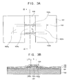
- FIG. 3A is a plan view illustrating a method of fabricating a TFT according to the exemplary embodiment of the present invention
- FIG. 3B is a cross-sectional view taken along line III-III of FIG. 3A
- a silicon layer 106 is formed on the exposed body contact region 102b and in direct contact with the body contact region 102b.
- the silicon layer 106 is also formed to cover the channel region 102c, on which the gate insulating layer 104 is formed, of the semiconductor layer 102.
- the silicon layer 106 is formed to a thickness of 100 ⁇ or more to prevent a direct connection between a gate metal of the gate electrode to be formed and the semiconductor layer 102, and formed to a thickness of 500 ⁇ or less in consideration of gate interconnection resistance and etch characteristics.
- the silicon layer 106 is doped with an impurity.
- the impurity injected into the silicon layer 106 has an opposite conductivity to those injected into the source and drain regions 102s and 102d in the semiconductor layer 102, i.e., the impurity injected into the silicon layer 106 has the same conductivity as the channel region 102c of the semiconductor layer 102. Accordingly, the silicon layer 106 is in direct contact with the body contact region 102b, which is formed in a PNP or NPN type together with the source and drain regions 102s and 102d. Thus, the silicon layer 106 prevents the flow of a current through the body contact region 102b from the source and drain regions 102s and 102d.
- the impurity may be a p- or n-type.
- the p-type impurity may be one selected from the group consisting of boron (B), aluminum (Al), gallium (Ga), and indium (In)
- the n-type impurity may be one selected from the group consisting of phosphorous (P), antimony (Sb), and arsenic (As).
- a gate electrode 108 is formed on the silicon layer 106.
- the gate electrode 108 is formed in a predetermined part corresponding to the semiconductor layer 102 by forming a metal layer (not illustrated) for a gate electrode, for example, a single layer formed of Al or an Al-Nd alloy on the silicon layer 106, or a multilayer formed of an aluminum alloy on a chromium (Cr) or molybdenum (Mo) alloy, and etching the metal layer for a gate electrode using photolithography to form the gate electrode 108.
- a metal layer not illustrated
- a gate electrode for example, a single layer formed of Al or an Al-Nd alloy on the silicon layer 106, or a multilayer formed of an aluminum alloy on a chromium (Cr) or molybdenum (Mo) alloy
- the gate electrode 108 is formed at a region corresponding to the channel region 102c, including the body contact region 102b, of the semiconductor layer 102, thereby defining the channel region 102c and the source and drain regions 102s and 102d in the semiconductor layer 102.
- the source and drain regions 102s and 102d are formed by injecting an impurity having an opposite conductivity type to that injected into the silicon layer 106 into regions to be the source and drain regions 102s and 102d of the semiconductor layer 102 using the gate electrode 108 as a mask. Additionally, the source and drain regions 102s and 102d may be formed by forming a photoresist pattern exposing the regions to be the source and drain regions and then injecting an impurity thereinto.
- the gate-body contact TFT is realized by making a contact between the gate electrode 108 and the body contact region 102b via the silicon layer 106 doped with the impurity.
- the gate insulating layer 104 is formed on the channel region 102c to expose the body contact region 102b of the edge region 102e of the semiconductor layer 102, and thus the body contact region 102b of the semiconductor layer 102 is in contact with the doped silicon layer 106. Consequently, a width "b" of the gate insulating layer 104 formed in the region corresponding to the channel region 102c is smaller than the sum of the widths of the channel region 102c and the body contact region 102b.
- a length direction with respect to the semiconductor layer 102 is a direction parallel to a line connecting a source region 102s with a drain region 102d of the semiconductor layer 102
- the width direction with respect to the semiconductor layer 102 is a direction perpendicular to a line connecting the source region 102s with the drain region 102d.
- a length is a distance parallel to a line between the source and drain regions in the semiconductor layer
- a width is a distance perpendicular to a line between the source and drain regions
- the silicon layer 106 doped with an impurity having an opposite conductivity type to the source and drain regions 102s and 102d are formed to electrically connect a region adjacent to the channel region 102c in the edge region 102e, so that the current cannot flow to the edge region 102e and the edge region 102e cannot be used as the channel region.
- the portion of the edge region 102e is used as a body contact region 102b for contact with the gate electrode 108, so that a gate-body contact TFT may be formed without the extension of a separate body contact region and without increasing the size of the gate-body contact TFT with respect to the conventional gate-body contact TFT.
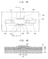
- FIG. 4A is a plan view illustrating a method of fabricating a TFT according to an exemplary embodiment of the present invention
- FIG. 4B is a cross-sectional view taken along line IV-IV of FIG. 4A
- an interlayer insulating layer 110 is formed on the entire surface of the substrate 100.
- the interlayer insulating layer 110 may be formed of silicon nitride, silicon oxide, or combinations thereof.
- the interlayer insulating layer 110 and the gate insulating layer 104 are etched so as to form a contact hole 113 for each of the source and drain regions 102s and 102d.
- the contact holes 113 expose the source and drain regions 102s and 102d of the semiconductor layer 102.
- source and drain electrodes 112a and 112b connected with the source and drain regions 102s and 102d through the contact holes 113 are formed.
- the source and drain electrodes 112a and 112b may be formed of one selected from the group consisting of molybdenum (Mo), chromium (Cr), tungsten (W), aluminum-neodymium (Al-Nd), titanium (Ti), molybdenum-tungsten (MoW), and aluminum (Al).
- Mo molybdenum
- Cr chromium
- W tungsten
- Al-Nd aluminum-neodymium
- Ti titanium
- MoW molybdenum-tungsten
- Al aluminum
- a process of gettering a crystallization-inducing metal in the semiconductor layer 102 using the silicon layer 106 doped with an impurity will be described.
- a polycrystalline silicon layer forming the semiconductor layer is crystallized by MIC, MILC, or SGS using a crystallization-inducing metal, and the crystallization-inducing metal remaining in the semiconductor layer 102 is gettered.
- the gettering process is to getter the crystallization-inducing metal remaining in the semiconductor layer 102, particularly, the region to be a channel region 102e, to the edge region 102e by annealing the n-type or p-type impurity injected into the silicon layer 102 in the above exemplary embodiments.
- the silicon layer 106 is in contact with the body contact region 102b, which is an edge region 102e of the semiconductor layer 102, and the channel region 102c, the crystallization-inducing metal remaining in the channel region 102c moves a short distance to the edge region 102e in the gettering process using the doped silicon layer 106, so that gettering efficiency may be significantly increased.
- the annealing process is performed for 30 seconds to 10 hours at a temperature ranging from 450 to 900°C.
- the temperature is less than 450°C, the crystallization-inducing metal remaining in the semiconductor layer 102 is difficult to be sufficiently removed, and when the temperature is more than 900°C, the substrate 100 may be deformed due to the high temperature.
- the annealing time is less than 30 seconds, the crystallization-inducing metal remaining in the semiconductor layer 102 is difficult to be sufficiently removed, and when the annealing time is more than 10 hours, the substrate 100 may be deformed due to the long annealing time, production cost may be increased, and yield of the TFT may be decreased.
- FIG. 5 is a cross-sectional view of an organic light emitting diode (OLED) display device having a TFT according to an exemplary embodiment of the present invention.
- OLED organic light emitting diode
- an insulating layer 114 is formed on the entire surface of the substrate 100 having the thin film transistor in FIG. 4 cut parallel to a source-drain direction, i.e., the length direction.
- the insulating layer 114 may be formed of an inorganic material selected from the group consisting of silicon oxide, silicon nitride, and silicate on glass, or an organic material selected from the group consisting of polyimide, benzocyclobutene series resin, and acrylate.
- the insulating layer 114 may be formed of a combination of the inorganic layer and the organic layer.
- the insulating layer 114 is etched, and thus a via hole 115 is formed to expose one of the source or drain electrodes 112a or 112b.
- a first electrode 116 connected with one of the source and drain electrodes 112a and 112b through the via hole 115 is formed.
- the first electrode 116 may be an anode or a cathode.
- the first electrode 116 may be a transparent conductive layer formed of one of ITO, IZO and ITZO.
- the first electrode 116 is a cathode, the first electrode 116 may be formed of Mg, Ca, Al, Ag, Ba, or alloys thereof.
- a pixel defining layer 118 having an opening to expose a part of a surface of the first electrode 116, is formed on the first electrode 116.
- An organic layer 120 having a light emitting layer is formed on the exposed part of the first electrode 116.
- the organic layer 120 may further include a hole injection layer, a hole transport layer, a hole blocking layer, an electron blocking layer, an electron injection layer, and an electron transport layer, but is not limited thereto.
- a second electrode 122 is formed on the organic layer 120.
- a thin film transistor, a method of fabricating the same, and an OLED display device having the same are provided.
- the gate-body contact TFT occupies a smaller area in a device than a conventional gate-body contact TFT structure by realizing a gate-body contact structure without a separately extended body contact region as in a conventional semiconductor layer region, which does not have a body contact region using an edge region of the semiconductor layer as a body contact region.
Landscapes
- Thin Film Transistor (AREA)
- Electroluminescent Light Sources (AREA)
Abstract
Description
- Aspects of the present invention relate to a thin film transistor, a method of fabricating the same and an organic light emitting diode (OLED) display device having the same.
- Generally, polycrystalline silicon layers are widely used as semiconductor layers for a thin film transistor because they have fast field effect mobility, and can be applied to a highspeed operation circuit and a complementary metal-oxide-semiconductor (CMOS) circuit. Thin film transistors using the polycrystalline silicon layer are used as a switching device of an active matrix liquid crystal display (AMLCD) device, and switching and driving devices of an active matrix organic light emitting diode (AMOLED) display device.
- The polycrystalline silicon (poly-Si) thin film transistors used in active matrix flat panel display devices, such as the AMLCD device or the AMOLED display device, are generally floating body poly-Si thin film transistors (TFT) in which a semiconductor layer is floated in the shape of an island. As the floating body poly-Si TFT gets smaller, a saturation region of a drain current is reduced, and the drain current is also reduced.
- In general, the semiconductor layer is formed of a polycrystalline silicon layer over the entire surface of the substrate, and a photoresist pattern is formed on the polycrystalline silicon layer. After that, the polycrystalline silicon layer is etched using the photoresist pattern as a mask, and the edge region of the semiconductor layer is damaged due to an etch solution or plasma used in the etching process. Further, the characteristics of the semiconductor layer become non-uniform or are degraded due to the remaining photoresist in the edge region. For this reason, the TFT having the semiconductor layer changes in characteristics, such as a threshold voltage or s-factor, and has a hump in an I-V curve, which shows the characteristics of the TFT. Such problems are caused by the damaged edge region used as the channel region.
- To solve these problems, a gate-body contact TFT in which a semiconductor layer is connected with a gate electrode has been suggested. In the gate-body contact TFT structure, a subthreshold slope value at a low gate voltage is improved, and a high drain current can be obtained at the low gate voltage. Thus, an on/off characteristic can be ensured at the low gate voltage, and a flat panel display device can be driven with low power consumption.
- Conventionally, to realize a gate-body contact thin film transistor, a separately extended body contact region for making a contact with a gate electrode is formed in a conventional semiconductor layer. However, the separately extended body contact region increases the area of the semiconductor layer, which is undesirable.
- Aspects of the present invention provide a gate-body contact TFT taking a smaller area in a device than a conventional gate-body contact TFT structure by realizing a gate-body contact structure without a separately extended body contact region in a conventional semiconductor layer region which does not have a body contact region using an edge region of the semiconductor layer as a body contact region, a method of fabricating the gate-body contact TFT, and an OLED display device having the same.
- According to aspects of the present invention, a TFT including a substrate; a semiconductor layer disposed on the substrate and having a channel region, source and drain regions and a body contact region; a gate insulating layer disposed on the semiconductor layer and exposing the body contact region; a silicon layer disposed on the gate insulating layer and in contact with the body contact region exposed by the gate insulating layer; a gate electrode disposed on the silicon layer; an interlayer insulating layer disposed on the gate electrode; and source and drain electrodes disposed on the interlayer insulating layer and electrically connected with the source and drain regions, wherein the body contact region is formed in an edge region of the semiconductor layer, a method of fabricating the same, and an OLED display device having the same are provided.
- Additional aspects and/or advantages of the invention will be set forth in part in the description which follows and, in part, will be obvious from the description, or may be learned by practice of the invention.
- These and/or other aspects and advantages of the invention will become apparent and more readily appreciated from the following description of the embodiments, taken in conjunction with the accompanying drawings of which:
-
FIGs. 1A to 4B are plan and cross-sectional views illustrating a method of fabricating a TFT according to an exemplary embodiment of the present invention, wherein theFIGs. 1A ,2A ,3A and4A are plan views, andFIGs. 1B ,2B ,3B and4B are cross-sectional views; and -
FIG. 5 is a cross-sectional view of an OLED display device having a TFT according to an exemplary embodiment of the present invention. - Reference will now be made in detail to aspects of the present invention, examples of which are illustrated in the accompanying drawings, wherein like reference numerals refer to the like elements throughout. The embodiments are described below in order to explain aspects of the present invention with reference to the figures.
-
FIG. 1A is a plan view illustrating a method of fabricating a TFT according to an exemplary embodiment of the present invention, andFIG. 1B is a cross-sectional view taken along line I-I ofFIG. 1A . Referring toFIGs. 1A and 1B , asubstrate 100 is provided. Thesubstrate 100 is formed of glass or plastic. Here, abuffer layer 101 is formed on thesubstrate 100. Thebuffer layer 101 serves to prevent diffusion of moisture or impurities generated from thesubstrate 100, or facilitate crystallization into a polycrystalline silicon layer to be formed in a following process by controlling a heat transfer rate during crystallization. Thebuffer layer 101 may be a single layer or comprised of multiple layers. - Subsequently, an amorphous silicon layer (not illustrated) is formed on the
buffer layer 101. Here, the amorphous silicon layer may be formed by chemical vapor deposition (CVD) or physical vapor deposition (PVD). Moreover, during the deposition, the amorphous silicon layer may be dehydrogenized to reduce a concentration of hydrogen therein. - After that, the amorphous silicon layer is crystallized into a polycrystalline silicon layer and patterned, thereby forming a
semiconductor layer 102. According to aspects of the present invention, a crystallization method using a metal catalyst is used to crystallize the amorphous silicon layer into the polycrystalline silicon layer. Such methods to crystallize the amorphous silicon layer into the polycrystalline silicon layer may include metal induced crystallization (MIC), metal induced lateral crystallization (MILC), or super grained silicon (SGS). A phosphorus (P)-injected silicon layer may be formed to remove a remaining metal catalyst from a portion of thesemiconductor layer 102 that corresponds to an area in which a channel region is to be formed. - MIC is a method that induces phase-change in an amorphous silicon layer into a polycrystalline silicon layer by contacting a metal catalyst, such as nickel, palladium, or aluminum, or by injecting the metal catalyst into the amorphous silicon layer. MILC is a method that induces sequential crystallization of an amorphous silicon layer into a polycrystalline silicon layer by lateral diffusion of silicide generated in a reaction of a metal catalyst and silicon.
- Further, SGS is a method for crystallizing an amorphous silicon layer into a polycrystalline silicon layer having larger-sized grains by forming a capping layer of silicon oxide, silicon nitride, or combinations thereof, to control diffusion or penetration of a metal catalyst into the amorphous silicon layer. A metal catalyst layer is formed on the capping layer and annealed. Upon annealing, the metal catalysts pass through the capping layer and diffuse onto a surface of the amorphous silicon layer to induce the crystallization of the amorphous silicon layer into the polycrystalline silicon layer. That is, the metal catalysts in the metal catalyst layer bind with silicon of the amorphous silicon layer, thereby forming metal silicide, which serves as a seed, i.e., a nucleus of crystallization, to induce the crystallization of the amorphous silicon layer.
- Accordingly, an amount of the metal silicide is controlled to control a grain size of the resultant polycrystalline silicon layer. Moreover, since the grain size is dependant on the metal catalyst layer contributing to the crystallization, the grain size of the polycrystalline silicon layer may be controlled by controlling a diffusion blocking ability of the capping layer. The metal catalyst may be one selected from the group consisting of Ni, Pd, Ti, Ag, Au, Al, Sn, Sb, Cu, Co, Mo, Tc, Ru, Rh, Cd and Pt, and may preferably be Ni. A concentration of the metal catalyst in the polycrystalline layer is about 5x10¹²atoms/cm2. The annealing process is performed at a temperature ranging from 400 to 1300°C, and may be performed by at least one of a furnace process, a rapid thermal annealing (RTA) process, an UV process, and a laser process.
- Subsequently, a
semiconductor layer 102 is formed by patterning the polycrystalline silicon layer. Here, since thesemiconductor layer 102 is formed of a polycrystalline silicon layer by a crystallization method using a metal catalyst, the metal catalyst remains in thesemiconductor layer 102. Thesemiconductor layer 102 includes source and drain regions, a channel region, and a body contact region corresponding to an edge region of thesemiconductor layer 102. Thesemiconductor layer 102 may include one or multiplebody contract regions 102b at the edge of thesemiconductor layer 102, and as shown inFIG. 2A , thebody contact regions 102b may be disposed atopposite edge regions 102e of thesemiconductor layer 102. -
Agate insulating layer 104 is formed on thesubstrate 100 and thegate insulating layer 104 is formed to cover thesemiconductor layer 102. Thegate insulating layer 104 may be formed of silicon oxide, silicon nitride, or combinations thereof. -
FIG. 2A is a plan view illustrating a method of fabricating a TFT according to an exemplary embodiment of the present invention, andFIG. 2B is a cross-sectional view taken along line II-II ofFIG. 2A . Referring toFIGs. 2A and 2B , a photoresist (not shown) is formed on thesubstrate 100 on which thegate insulating layer 104 and thesemiconductor layer 102 are formed, and then the photoresist is exposed to form aphotoresist pattern 105. Portions of thephotoresist pattern 105 are removed to expose a portion of thegate insulating layer 104 that is to be removed, i.e., the exposedpart 104R. The exposedpart 104R covers a portion of theedge region 102e of thesemiconductor layer 102. The exposedpart 104R of thegate insulating layer 104 is removed by etching to expose a portion of theedge region 102e of thesemiconductor layer 102, i.e., thebody contact regions 102b. Then, thephotoresist pattern 105 is removed, thereby forming a structure having an exposedbody contact region 102b of thesemiconductor layer 102. - Here, the
body contact region 102b of theedge region 102e of thesemiconductor layer 102 to be exposed is a region spaced apart by a predetermined distance "a" in a width direction from an edge of thesemiconductor layer 102. The portion to be exposed to form thebody contact region 102b may be singular or plural, may extend inward from opposing edges of thesemiconductor layer 102c, and may extend inward in a width direction from opposing edges of thesemiconductor layer 102c. InFIG. 2A , the width direction is parallel to the line II-II while the length direction is perpendicular to the line II-II. - The predetermined width a of the
edge region 102e may be more than 0 and not more than 0.1µm. In this range of the width, a gate-body contact TFT structure may be formed without reducing an area of the channel region of the conventional semiconductor layer and separately forming an extended body contact region. Further, thebody contact region 102b in theedge region 102e will have a predetermined length t a' and be adjacent to thechannel region 102c. Thus, inFIG. 2A , thebody contact regions 102b have areas of axa'. -
FIG. 3A is a plan view illustrating a method of fabricating a TFT according to the exemplary embodiment of the present invention, andFIG. 3B is a cross-sectional view taken along line III-III ofFIG. 3A . Referring toFIGs. 3A and 3B , asilicon layer 106 is formed on the exposedbody contact region 102b and in direct contact with thebody contact region 102b. Thesilicon layer 106 is also formed to cover thechannel region 102c, on which thegate insulating layer 104 is formed, of thesemiconductor layer 102. Here, thesilicon layer 106 is formed to a thickness of 100Å or more to prevent a direct connection between a gate metal of the gate electrode to be formed and thesemiconductor layer 102, and formed to a thickness of 500Å or less in consideration of gate interconnection resistance and etch characteristics. - After that, the
silicon layer 106 is doped with an impurity. The impurity injected into thesilicon layer 106 has an opposite conductivity to those injected into the source anddrain regions semiconductor layer 102, i.e., the impurity injected into thesilicon layer 106 has the same conductivity as thechannel region 102c of thesemiconductor layer 102. Accordingly, thesilicon layer 106 is in direct contact with thebody contact region 102b, which is formed in a PNP or NPN type together with the source anddrain regions silicon layer 106 prevents the flow of a current through thebody contact region 102b from the source anddrain regions - Then, a
gate electrode 108 is formed on thesilicon layer 106. Thegate electrode 108 is formed in a predetermined part corresponding to thesemiconductor layer 102 by forming a metal layer (not illustrated) for a gate electrode, for example, a single layer formed of Al or an Al-Nd alloy on thesilicon layer 106, or a multilayer formed of an aluminum alloy on a chromium (Cr) or molybdenum (Mo) alloy, and etching the metal layer for a gate electrode using photolithography to form thegate electrode 108. Here, thegate electrode 108 is formed at a region corresponding to thechannel region 102c, including thebody contact region 102b, of thesemiconductor layer 102, thereby defining thechannel region 102c and the source anddrain regions semiconductor layer 102. - Specifically, the source and
drain regions silicon layer 106 into regions to be the source anddrain regions semiconductor layer 102 using thegate electrode 108 as a mask. Additionally, the source anddrain regions - Thus, the gate-body contact TFT is realized by making a contact between the
gate electrode 108 and thebody contact region 102b via thesilicon layer 106 doped with the impurity. According to aspects of the present invention, thegate insulating layer 104 is formed on thechannel region 102c to expose thebody contact region 102b of theedge region 102e of thesemiconductor layer 102, and thus thebody contact region 102b of thesemiconductor layer 102 is in contact with the dopedsilicon layer 106. Consequently, a width "b" of thegate insulating layer 104 formed in the region corresponding to thechannel region 102c is smaller than the sum of the widths of thechannel region 102c and thebody contact region 102b.
Similar to as described above, a length direction with respect to thesemiconductor layer 102 is a direction parallel to a line connecting asource region 102s with adrain region 102d of thesemiconductor layer 102, and the width direction with respect to thesemiconductor layer 102 is a direction perpendicular to a line connecting thesource region 102s with thedrain region 102d. Herein, a length is a distance parallel to a line between the source and drain regions in the semiconductor layer, and a width is a distance perpendicular to a line between the source and drain regions - According to aspects of the present invention, the
silicon layer 106 doped with an impurity having an opposite conductivity type to the source anddrain regions channel region 102c in theedge region 102e, so that the current cannot flow to theedge region 102e and theedge region 102e cannot be used as the channel region. Moreover, according to aspects of the present invention, the portion of theedge region 102e is used as abody contact region 102b for contact with thegate electrode 108, so that a gate-body contact TFT may be formed without the extension of a separate body contact region and without increasing the size of the gate-body contact TFT with respect to the conventional gate-body contact TFT. -
FIG. 4A is a plan view illustrating a method of fabricating a TFT according to an exemplary embodiment of the present invention, andFIG. 4B is a cross-sectional view taken along line IV-IV ofFIG. 4A . Referring toFIGs. 4A and 4B , aninterlayer insulating layer 110 is formed on the entire surface of thesubstrate 100. The interlayer insulatinglayer 110 may be formed of silicon nitride, silicon oxide, or combinations thereof. - Then, the
interlayer insulating layer 110 and thegate insulating layer 104 are etched so as to form acontact hole 113 for each of the source anddrain regions drain regions semiconductor layer 102. After that, source anddrain electrodes drain regions drain electrodes - In another exemplary embodiment of the present invention, a process of gettering a crystallization-inducing metal in the
semiconductor layer 102 using thesilicon layer 106 doped with an impurity will be described. A polycrystalline silicon layer forming the semiconductor layer is crystallized by MIC, MILC, or SGS using a crystallization-inducing metal, and the crystallization-inducing metal remaining in thesemiconductor layer 102 is gettered. - The gettering process is to getter the crystallization-inducing metal remaining in the
semiconductor layer 102, particularly, the region to be achannel region 102e, to theedge region 102e by annealing the n-type or p-type impurity injected into thesilicon layer 102 in the above exemplary embodiments. - Since, in the exemplary embodiments of the present invention, the
silicon layer 106 is in contact with thebody contact region 102b, which is anedge region 102e of thesemiconductor layer 102, and thechannel region 102c, the crystallization-inducing metal remaining in thechannel region 102c moves a short distance to theedge region 102e in the gettering process using the dopedsilicon layer 106, so that gettering efficiency may be significantly increased. - The annealing process is performed for 30 seconds to 10 hours at a temperature ranging from 450 to 900°C. When the temperature is less than 450°C, the crystallization-inducing metal remaining in the
semiconductor layer 102 is difficult to be sufficiently removed, and when the temperature is more than 900°C, thesubstrate 100 may be deformed due to the high temperature. Also, when the annealing time is less than 30 seconds, the crystallization-inducing metal remaining in thesemiconductor layer 102 is difficult to be sufficiently removed, and when the annealing time is more than 10 hours, thesubstrate 100 may be deformed due to the long annealing time, production cost may be increased, and yield of the TFT may be decreased. -
FIG. 5 is a cross-sectional view of an organic light emitting diode (OLED) display device having a TFT according to an exemplary embodiment of the present invention. Referring toFIG. 5 , an insulatinglayer 114 is formed on the entire surface of thesubstrate 100 having the thin film transistor inFIG. 4 cut parallel to a source-drain direction, i.e., the length direction. The insulatinglayer 114 may be formed of an inorganic material selected from the group consisting of silicon oxide, silicon nitride, and silicate on glass, or an organic material selected from the group consisting of polyimide, benzocyclobutene series resin, and acrylate. Alternatively, the insulatinglayer 114 may be formed of a combination of the inorganic layer and the organic layer. - The insulating
layer 114 is etched, and thus a viahole 115 is formed to expose one of the source ordrain electrodes first electrode 116 connected with one of the source anddrain electrodes hole 115 is formed. Thefirst electrode 116 may be an anode or a cathode. When thefirst electrode 116 is an anode, thefirst electrode 116 may be a transparent conductive layer formed of one of ITO, IZO and ITZO. When thefirst electrode 116 is a cathode, thefirst electrode 116 may be formed of Mg, Ca, Al, Ag, Ba, or alloys thereof. - Subsequently, a
pixel defining layer 118, having an opening to expose a part of a surface of thefirst electrode 116, is formed on thefirst electrode 116. Anorganic layer 120 having a light emitting layer is formed on the exposed part of thefirst electrode 116. Theorganic layer 120 may further include a hole injection layer, a hole transport layer, a hole blocking layer, an electron blocking layer, an electron injection layer, and an electron transport layer, but is not limited thereto. Then, asecond electrode 122 is formed on theorganic layer 120. Thus, an OLED display device according to the exemplary embodiment of the present invention is completed. - According to aspects of the present invention, a thin film transistor, a method of fabricating the same, and an OLED display device having the same are provided. The gate-body contact TFT occupies a smaller area in a device than a conventional gate-body contact TFT structure by realizing a gate-body contact structure without a separately extended body contact region as in a conventional semiconductor layer region, which does not have a body contact region using an edge region of the semiconductor layer as a body contact region.
- Although a few embodiments of the present invention have been shown and described, it would be appreciated by those skilled in the art that changes may be made in this embodiment without departing from the scope of the claims and their equivalents.
Claims (15)
- A thin film transistor, comprising:a substrate (100);a semiconductor layer (102) disposed on the substrate (100), comprising a channel region (102c), source (102s) and drain regions (102d), and a first body contact region (102b) formed at a first edge of the semiconductor layer (102);a gate insulating layer (104) disposed on the channel region (102c) of the semiconductor layer (102) exposing the first body contact region (102b);a silicon layer (106) disposed on the gate insulating layer (104) and the first body contact region (102b), the silicon layer (106) contacting the first body contact region (102b);a gate electrode (108) disposed on the silicon layer (106);an interlayer insulating layer (110) disposed on the gate electrode (108) and the gate insulating layer (104); andsource and drain electrodes (112a, 112b) disposed on the interlayer insulating layer and electrically connected with the source and drain regions (102s, 102d), respectively.
- The thin film transistor according to claim 1, wherein the first body contact region (102b) is connected with the channel region (102c).
- The thin film transistor according to one of the claims 1 or 2, wherein the silicon layer (102) includes a first type of impurity, and the source and drain regions (102s, 102d) include a second type of impurity, the first and second types of impurities having opposite conductivities.
- The thin film transistor according to claim 3, wherein the first type of impurity is an n-type impurity, and the semiconductor layer is crystallized using a crystallization-inducing metal.
- The thin film transistor according to one of the preceding claims, wherein a width of the gate insulating layer (104) formed on the channel region (102c) of the semiconductor layer (102) is less than the width of the semiconductor layer (102).
- The thin film transistor according to one of the preceding claims, wherein a width of the body contact region (102b) is more than 0 and not more than 0.1µm.
- The thin film transistor according to one of the preceding claims, wherein the semiconductor layer (102) further comprises a second body contact region (102b) formed at a second edge of the semiconductor layer (102), the second edge of the semiconductor layer being opposite the first edge of the semiconductor layer (102).
- The thin film transistor according to claim 7, wherein the first and second body contact regions (102b) have a same length as the channel region (102c) of the semiconductor layer (102).
- The thin film transistor according to one of the claims 7 or 8, wherein the silicon layer (106) covers the channel region (102c) and the first and second body contact regions (102b).
- A method of fabricating a thin film transistor according to one of the preceding claims, comprising:forming a semiconductor layer (102) on a substrate (100);forming a gate insulating layer (104) on a channel region (102c) of the semiconductor layer (102) exposing a first body contact region (102b) formed at a first edge of the semiconductor layer (102);forming a silicon layer (106) on the gate insulating layer (104) and the first body contact region (102b), the silicon layer (106) contacting the first body contact region (102b);injecting an impurity into the silicon layer (102);forming a gate electrode (108) on the silicon layer (106);forming an interlayer insulating layer (110) on the gate electrode and the gate insulating layer (104); andforming source and drain electrodes (112a, 112b) on the interlayer insulating layer (110) electrically connected to source and drain regions (1 02s, 102d) of the semiconductor layer (102).
- The method according to claim 10, wherein the injecting of the impurity into the silicon layer (102) further comprises:injecting an impurity having a conductivity type opposite to a conductivity type of an impurity in source and drain regions (1 02s, 102d) of the semiconductor layer (102).
- The method according to one of the claims 10 or 11, wherein the injecting of the impurity into the silicon layer (102) further comprises:injecting the impurity into the silicon layer (102) using the gate electrode (108) as a mask.
- The method according to one of the claims 10 through 12, further comprising:forming the semiconductor layer (102) by crystallizing an amorphous silicon layer into a polycrystalline silicon layer using a crystallization-inducting metal;injecting an n-type impurity into the first body contact region (102) of the semiconductor layer (102) using the gate insulating layer (108) as a mask; andannealing the substrate (100) and gettering the crystallization-inducing metal remaining in the semiconductor layer (102) to the region into which the n-type impurity is injected.
- The method according to claim 13, wherein the substrate (100) is annealed for about 30 seconds to 10 hours at a temperature of about 450 to 900°C.
- An organic light emitting diode (OLED) display device, comprising a thin film transistor according to one of the claims 1 through 9.
Applications Claiming Priority (1)
| Application Number | Priority Date | Filing Date | Title |
|---|---|---|---|
| KR1020080033818A KR100989136B1 (en) | 2008-04-11 | 2008-04-11 | Thin film transistor, manufacturing method thereof, and organic light emitting display device comprising the same |
Publications (3)
| Publication Number | Publication Date |
|---|---|
| EP2117048A2 true EP2117048A2 (en) | 2009-11-11 |
| EP2117048A3 EP2117048A3 (en) | 2010-03-31 |
| EP2117048B1 EP2117048B1 (en) | 2017-06-14 |
Family
ID=40942811
Family Applications (1)
| Application Number | Title | Priority Date | Filing Date |
|---|---|---|---|
| EP09157829.4A Not-in-force EP2117048B1 (en) | 2008-04-11 | 2009-04-14 | Thin film transistor, method of fabricating the same and organic light emitting diode display device having the same |
Country Status (5)
| Country | Link |
|---|---|
| US (1) | US8318523B2 (en) |
| EP (1) | EP2117048B1 (en) |
| JP (1) | JP5126849B2 (en) |
| KR (1) | KR100989136B1 (en) |
| CN (1) | CN101556968B (en) |
Cited By (1)
| Publication number | Priority date | Publication date | Assignee | Title |
|---|---|---|---|---|
| TWI495044B (en) * | 2010-01-14 | 2015-08-01 | 三星顯示器有限公司 | Organic light emitting diode display and method of manufacturing same |
Families Citing this family (11)
| Publication number | Priority date | Publication date | Assignee | Title |
|---|---|---|---|---|
| KR100875432B1 (en) | 2007-05-31 | 2008-12-22 | 삼성모바일디스플레이주식회사 | Method for manufacturing polycrystalline silicon layer, thin film transistor formed using same, method for manufacturing thereof and organic light emitting display device comprising same |
| CN101840936B (en) * | 2009-02-13 | 2014-10-08 | 株式会社半导体能源研究所 | Semiconductor device including a transistor, and manufacturing method of the semiconductor device |
| KR101050467B1 (en) * | 2010-04-14 | 2011-07-20 | 삼성모바일디스플레이주식회사 | A polycrystalline silicon layer, a manufacturing method thereof, a thin film transistor using the polycrystalline silicide layer, and an organic light emitting display device having the thin film transistor |
| KR101809661B1 (en) * | 2011-06-03 | 2017-12-18 | 삼성디스플레이 주식회사 | Thin film transistor, manufacturing method of thin film transistor, and organic light emitting diode display including the same |
| KR101860859B1 (en) | 2011-06-13 | 2018-05-25 | 삼성디스플레이 주식회사 | Manufacturing method of thin film transistor, the thin film transistor manufactured by the same, manufacturing method of organic light emitting apparatus and the organic light emitting apparatus manufactured by the same |
| KR101829312B1 (en) * | 2011-08-26 | 2018-02-20 | 삼성디스플레이 주식회사 | Organic light emitting display device and the manufacturing method thereof |
| TWI621270B (en) * | 2013-02-07 | 2018-04-11 | 群創光電股份有限公司 | Thin film transistor element and thin film transistor display device |
| KR20150010065A (en) * | 2013-07-18 | 2015-01-28 | 삼성디스플레이 주식회사 | Method of forming an oxide semiconductor device, and method of manufacturing a display device having an oxide semiconductor device |
| KR20170080996A (en) * | 2015-12-31 | 2017-07-11 | 삼성디스플레이 주식회사 | Thin film transistor for display device and organic light emitting diode display device comprising the same |
| CN110060998B (en) * | 2019-04-29 | 2022-05-17 | 厦门天马微电子有限公司 | Inverter circuit structure, gate drive circuit and display panel |
| CN111244110B (en) * | 2020-01-19 | 2023-04-18 | 深圳市华星光电半导体显示技术有限公司 | Display panel and electronic device |
Family Cites Families (100)
| Publication number | Priority date | Publication date | Assignee | Title |
|---|---|---|---|---|
| US3465209A (en) * | 1966-07-07 | 1969-09-02 | Rca Corp | Semiconductor devices and methods of manufacture thereof |
| JPS62104173A (en) * | 1985-10-31 | 1987-05-14 | Fujitsu Ltd | Semiconductor device |
| JP3122177B2 (en) | 1991-08-09 | 2001-01-09 | 旭硝子株式会社 | Thin film transistor and manufacturing method thereof |
| JPH06151859A (en) * | 1992-09-15 | 1994-05-31 | Canon Inc | Semiconductor device |
| TW232751B (en) * | 1992-10-09 | 1994-10-21 | Semiconductor Energy Res Co Ltd | Semiconductor device and method for forming the same |
| JP2762215B2 (en) * | 1993-08-12 | 1998-06-04 | 株式会社半導体エネルギー研究所 | Method for manufacturing thin film transistor and semiconductor device |
| JPH07176753A (en) | 1993-12-17 | 1995-07-14 | Semiconductor Energy Lab Co Ltd | Thin-film semiconductor device and its manufacture |
| JP3403807B2 (en) | 1994-06-02 | 2003-05-06 | 松下電器産業株式会社 | Thin film transistor and liquid crystal display |
| JP2738315B2 (en) * | 1994-11-22 | 1998-04-08 | 日本電気株式会社 | Thin film transistor and method of manufacturing the same |
| JPH08255907A (en) | 1995-01-18 | 1996-10-01 | Canon Inc | Insulated gate transistor and manufacturing method thereof |
| US5771110A (en) * | 1995-07-03 | 1998-06-23 | Sanyo Electric Co., Ltd. | Thin film transistor device, display device and method of fabricating the same |
| JP3744980B2 (en) * | 1995-07-27 | 2006-02-15 | 株式会社半導体エネルギー研究所 | Semiconductor device |
| TW374196B (en) * | 1996-02-23 | 1999-11-11 | Semiconductor Energy Lab Co Ltd | Semiconductor thin film and method for manufacturing the same and semiconductor device and method for manufacturing the same |
| JPH1012882A (en) | 1996-06-20 | 1998-01-16 | Toshiba Corp | Thin film transistor and method of manufacturing the same |
| US6746905B1 (en) * | 1996-06-20 | 2004-06-08 | Kabushiki Kaisha Toshiba | Thin film transistor and manufacturing process therefor |
| TW324862B (en) | 1996-07-03 | 1998-01-11 | Hitachi Ltd | Liquid display apparatus |
| JPH10150204A (en) * | 1996-09-19 | 1998-06-02 | Toshiba Corp | Semiconductor device and manufacturing method thereof |
| JPH10135475A (en) * | 1996-10-31 | 1998-05-22 | Semiconductor Energy Lab Co Ltd | Semiconductor device and manufacturing method thereof |
| JP3545583B2 (en) * | 1996-12-26 | 2004-07-21 | 株式会社ルネサステクノロジ | Semiconductor device and manufacturing method thereof |
| TW386238B (en) * | 1997-01-20 | 2000-04-01 | Semiconductor Energy Lab | Semiconductor device and method of manufacturing the same |
| JP3942683B2 (en) | 1997-02-12 | 2007-07-11 | 株式会社半導体エネルギー研究所 | Semiconductor device manufacturing method |
| JP3544280B2 (en) * | 1997-03-27 | 2004-07-21 | 株式会社半導体エネルギー研究所 | Method for manufacturing semiconductor device |
| JP3717634B2 (en) | 1997-06-17 | 2005-11-16 | 株式会社半導体エネルギー研究所 | Method for manufacturing semiconductor device |
| JPH11111992A (en) | 1997-09-30 | 1999-04-23 | Toshiba Corp | Thin film transistor, complementary thin film transistor, and method of manufacturing thin film transistor |
| US6369410B1 (en) * | 1997-12-15 | 2002-04-09 | Semiconductor Energy Laboratory Co., Ltd. | Semiconductor device and method of manufacturing the semiconductor device |
| JPH11261075A (en) | 1998-03-13 | 1999-09-24 | Semiconductor Energy Lab Co Ltd | Semiconductor device and its manufacture |
| KR19990075412A (en) | 1998-03-20 | 1999-10-15 | 윤종용 | Thin film transistor and method of manufacturing the same |
| US6331476B1 (en) | 1998-05-26 | 2001-12-18 | Mausushita Electric Industrial Co., Ltd. | Thin film transistor and producing method thereof |
| CN100373563C (en) * | 1998-06-30 | 2008-03-05 | 东芝松下显示技术有限公司 | Method for manufacturing top gate type thin film transistor |
| US6346437B1 (en) * | 1998-07-16 | 2002-02-12 | Sharp Laboratories Of America, Inc. | Single crystal TFT from continuous transition metal delivery method |
| JP4030193B2 (en) | 1998-07-16 | 2008-01-09 | 株式会社半導体エネルギー研究所 | Method for manufacturing semiconductor device |
| JP4376331B2 (en) | 1998-08-07 | 2009-12-02 | 株式会社半導体エネルギー研究所 | Method for manufacturing semiconductor device |
| US6559036B1 (en) * | 1998-08-07 | 2003-05-06 | Semiconductor Energy Laboratory Co., Ltd. | Semiconductor device and method of manufacturing the same |
| JP4531177B2 (en) | 1998-12-28 | 2010-08-25 | 株式会社半導体エネルギー研究所 | Method for manufacturing semiconductor device |
| US6380007B1 (en) * | 1998-12-28 | 2002-04-30 | Semiconductor Energy Laboratory Co., Ltd. | Semiconductor device and manufacturing method of the same |
| KR100303711B1 (en) | 1999-01-28 | 2001-09-26 | 장 진 | Thin film transistor with polycrystalline/amorphous double active layers |
| KR20010043359A (en) * | 1999-03-10 | 2001-05-25 | 모리시타 요이찌 | Thin-film transistor, panel, and methods for producing them |
| US6680487B1 (en) | 1999-05-14 | 2004-01-20 | Semiconductor Energy Laboratory Co., Ltd. | Semiconductor comprising a TFT provided on a substrate having an insulating surface and method of fabricating the same |
| JP4270719B2 (en) | 1999-06-30 | 2009-06-03 | 株式会社東芝 | Semiconductor device and manufacturing method thereof |
| JP4437570B2 (en) * | 1999-07-12 | 2010-03-24 | 株式会社ルネサステクノロジ | Semiconductor device and manufacturing method of semiconductor device |
| JP2001102169A (en) * | 1999-10-01 | 2001-04-13 | Sanyo Electric Co Ltd | EL display device |
| US20020020840A1 (en) | 2000-03-10 | 2002-02-21 | Setsuo Nakajima | Semiconductor device and manufacturing method thereof |
| TWI301907B (en) * | 2000-04-03 | 2008-10-11 | Semiconductor Energy Lab | Semiconductor device, liquid crystal display device and manfacturing method thereof |
| JP2001319878A (en) | 2000-05-11 | 2001-11-16 | Sharp Corp | Semiconductor manufacturing method |
| JP2002093745A (en) * | 2000-09-12 | 2002-03-29 | Matsushita Electric Ind Co Ltd | Method for manufacturing semiconductor device |
| KR100439345B1 (en) * | 2000-10-31 | 2004-07-07 | 피티플러스(주) | Thin film transistor including a polycrystalline active layer and method making same |
| US7045444B2 (en) * | 2000-12-19 | 2006-05-16 | Semiconductor Energy Laboratory Co., Ltd. | Method of manufacturing semiconductor device that includes selectively adding a noble gas element |
| TW546846B (en) * | 2001-05-30 | 2003-08-11 | Matsushita Electric Industrial Co Ltd | Thin film transistor and method for manufacturing the same |
| US6743700B2 (en) * | 2001-06-01 | 2004-06-01 | Semiconductor Energy Laboratory Co., Ltd. | Semiconductor film, semiconductor device and method of their production |
| JP2003007719A (en) * | 2001-06-21 | 2003-01-10 | Matsushita Electric Ind Co Ltd | Thin film transistor and display device using the same |
| JP3961240B2 (en) * | 2001-06-28 | 2007-08-22 | 株式会社半導体エネルギー研究所 | Method for manufacturing semiconductor device |
| KR100662493B1 (en) * | 2001-07-10 | 2007-01-02 | 엘지.필립스 엘시디 주식회사 | Crystallization method of amorphous film and manufacturing method of liquid crystal display device using same |
| US6952023B2 (en) * | 2001-07-17 | 2005-10-04 | Semiconductor Energy Laboratory Co., Ltd. | Light emitting device |
| JP2003075870A (en) | 2001-09-06 | 2003-03-12 | Toshiba Corp | Flat display device and method of manufacturing the same |
| JP2003100633A (en) | 2001-09-25 | 2003-04-04 | Sharp Corp | Semiconductor device manufacturing method and semiconductor device |
| JP3600229B2 (en) | 2001-10-31 | 2004-12-15 | 株式会社半導体エネルギー研究所 | Method for manufacturing field effect transistor |
| JP2003188098A (en) | 2001-12-13 | 2003-07-04 | Sharp Corp | Semiconductor device and method of manufacturing the same |
| US20030155572A1 (en) * | 2002-02-19 | 2003-08-21 | Min-Koo Han | Thin film transistor and method for manufacturing thereof |
| JP2003298059A (en) | 2002-03-29 | 2003-10-17 | Advanced Lcd Technologies Development Center Co Ltd | Thin film transistor |
| JP4115153B2 (en) | 2002-04-08 | 2008-07-09 | シャープ株式会社 | Manufacturing method of semiconductor device |
| JP4115158B2 (en) | 2002-04-24 | 2008-07-09 | シャープ株式会社 | Semiconductor device and manufacturing method thereof |
| JP2004022845A (en) | 2002-06-17 | 2004-01-22 | Sharp Corp | Thin film transistor, method of manufacturing the same, and display device |
| JP4115283B2 (en) * | 2003-01-07 | 2008-07-09 | シャープ株式会社 | Semiconductor device and manufacturing method thereof |
| KR100928490B1 (en) * | 2003-06-28 | 2009-11-26 | 엘지디스플레이 주식회사 | LCD panel and manufacturing method thereof |
| JP2005057240A (en) * | 2003-07-23 | 2005-03-03 | Seiko Epson Corp | Thin film semiconductor device and method for manufacturing thin film semiconductor device |
| KR100515357B1 (en) | 2003-08-14 | 2005-09-15 | 삼성에스디아이 주식회사 | Gate-shorted-to-body thin film transistor and manufacturing method thereof |
| KR100501706B1 (en) | 2003-10-16 | 2005-07-18 | 삼성에스디아이 주식회사 | Gate-body contact TFT |
| US7202143B1 (en) * | 2003-10-23 | 2007-04-10 | The Board Of Trustees Of The University Of Arkansas | Low temperature production of large-grain polycrystalline semiconductors |
| KR100600853B1 (en) * | 2003-11-17 | 2006-07-14 | 삼성에스디아이 주식회사 | Flat panel display and manufacturing method |
| KR100611224B1 (en) | 2003-11-22 | 2006-08-09 | 삼성에스디아이 주식회사 | Thin film transistor using metal induced lateral crystallization and its manufacturing method |
| KR100623247B1 (en) | 2003-12-22 | 2006-09-18 | 삼성에스디아이 주식회사 | Flat panel display and manufacturing method |
| KR100595456B1 (en) * | 2003-12-29 | 2006-06-30 | 엘지.필립스 엘시디 주식회사 | Manufacturing method of liquid crystal display device |
| JP4437404B2 (en) * | 2004-01-08 | 2010-03-24 | シャープ株式会社 | Semiconductor device and manufacturing method thereof |
| KR100654022B1 (en) * | 2004-05-04 | 2006-12-04 | 네오폴리((주)) | Method of manufacturing thin film transistor using metal guided side crystallization |
| KR200357656Y1 (en) | 2004-05-19 | 2004-07-31 | 한국해양연구원 | Prevention system of a corruption |
| TW200601566A (en) * | 2004-06-28 | 2006-01-01 | Adv Lcd Tech Dev Ct Co Ltd | Semiconductor apparatus and manufacturing method thereof |
| JP2006049823A (en) | 2004-06-28 | 2006-02-16 | Advanced Lcd Technologies Development Center Co Ltd | Semiconductor device and its manufacturing method |
| KR100656495B1 (en) * | 2004-08-13 | 2006-12-11 | 삼성에스디아이 주식회사 | Thin film transistor and its manufacturing method |
| US20060040438A1 (en) * | 2004-08-17 | 2006-02-23 | Jiong-Ping Lu | Method for improving the thermal stability of silicide |
| KR200369779Y1 (en) | 2004-08-18 | 2004-12-16 | 서성탁 | A cut-off of flowing backward of stench and insect using the trap from a sewer pipe |
| KR100611766B1 (en) | 2004-08-24 | 2006-08-10 | 삼성에스디아이 주식회사 | Method of manufacturing thin film transistor |
| KR200373075Y1 (en) | 2004-10-12 | 2005-01-15 | 장한규 | Wash board |
| KR200373076Y1 (en) | 2004-10-12 | 2005-01-15 | 황금수 | Blade fixing unit for a wood chipper and its blade |
| US7575959B2 (en) * | 2004-11-26 | 2009-08-18 | Semiconductor Energy Laboratory Co., Ltd. | Manufacturing method of semiconductor device |
| KR200384738Y1 (en) | 2005-03-02 | 2005-05-17 | 박현우 | Orange color candle |
| US8088676B2 (en) * | 2005-04-28 | 2012-01-03 | The Hong Kong University Of Science And Technology | Metal-induced crystallization of amorphous silicon, polycrystalline silicon thin films produced thereby and thin film transistors produced therefrom |
| KR100741976B1 (en) * | 2005-08-25 | 2007-07-23 | 삼성에스디아이 주식회사 | Thin film transistor and its manufacturing method |
| JP5386064B2 (en) * | 2006-02-17 | 2014-01-15 | 株式会社半導体エネルギー研究所 | Method for manufacturing semiconductor device |
| JP5670005B2 (en) * | 2006-03-06 | 2015-02-18 | ピーエスフォー ルクスコ エスエイアールエルPS4 Luxco S.a.r.l. | Semiconductor device and manufacturing method thereof |
| TWI429028B (en) * | 2006-03-31 | 2014-03-01 | 半導體能源研究所股份有限公司 | Non-volatile semiconductor memory device and method of manufacturing same |
| KR100770268B1 (en) | 2006-05-18 | 2007-10-25 | 삼성에스디아이 주식회사 | Method of manufacturing thin film transistor |
| KR101362955B1 (en) | 2006-06-30 | 2014-02-12 | 가부시키가이샤 한도오따이 에네루기 켄큐쇼 | Semiconductor device and manufacturing method thereof |
| JP4481284B2 (en) | 2006-09-20 | 2010-06-16 | 株式会社半導体エネルギー研究所 | Method for manufacturing semiconductor device |
| KR100878284B1 (en) * | 2007-03-09 | 2009-01-12 | 삼성모바일디스플레이주식회사 | Thin film transistor, manufacturing method thereof and organic light emitting display device having same |
| KR100846985B1 (en) * | 2007-04-06 | 2008-07-17 | 삼성에스디아이 주식회사 | Organic electroluminescent display and manufacturing method thereof |
| KR100875432B1 (en) | 2007-05-31 | 2008-12-22 | 삼성모바일디스플레이주식회사 | Method for manufacturing polycrystalline silicon layer, thin film transistor formed using same, method for manufacturing thereof and organic light emitting display device comprising same |
| KR101383409B1 (en) * | 2007-06-08 | 2014-04-18 | 엘지디스플레이 주식회사 | display device |
| KR100848341B1 (en) | 2007-06-13 | 2008-07-25 | 삼성에스디아이 주식회사 | Thin film transistor, manufacturing method thereof, and organic light emitting display device comprising the same |
| KR100889627B1 (en) | 2007-08-23 | 2009-03-20 | 삼성모바일디스플레이주식회사 | Thin film transistor, manufacturing method thereof, and organic light emitting display device having same |
| KR100982310B1 (en) | 2008-03-27 | 2010-09-15 | 삼성모바일디스플레이주식회사 | TFT, fabricating methode of the TFT, and organic lighting emitting diode display device comprising the same |
-
2008
- 2008-04-11 KR KR1020080033818A patent/KR100989136B1/en active Active
- 2008-11-07 JP JP2008286941A patent/JP5126849B2/en active Active
-
2009
- 2009-03-17 US US12/405,466 patent/US8318523B2/en active Active
- 2009-04-10 CN CN200910134258XA patent/CN101556968B/en not_active Expired - Fee Related
- 2009-04-14 EP EP09157829.4A patent/EP2117048B1/en not_active Not-in-force
Cited By (1)
| Publication number | Priority date | Publication date | Assignee | Title |
|---|---|---|---|---|
| TWI495044B (en) * | 2010-01-14 | 2015-08-01 | 三星顯示器有限公司 | Organic light emitting diode display and method of manufacturing same |
Also Published As
| Publication number | Publication date |
|---|---|
| CN101556968B (en) | 2011-12-21 |
| JP5126849B2 (en) | 2013-01-23 |
| EP2117048A3 (en) | 2010-03-31 |
| US8318523B2 (en) | 2012-11-27 |
| EP2117048B1 (en) | 2017-06-14 |
| KR20090108416A (en) | 2009-10-15 |
| CN101556968A (en) | 2009-10-14 |
| KR100989136B1 (en) | 2010-10-20 |
| JP2009260239A (en) | 2009-11-05 |
| US20090256469A1 (en) | 2009-10-15 |
Similar Documents
| Publication | Publication Date | Title |
|---|---|---|
| EP2117048B1 (en) | Thin film transistor, method of fabricating the same and organic light emitting diode display device having the same | |
| CN101373792B (en) | Thin film transistor, organic light emitting diode display device, and method of fabricating the same | |
| US7999261B2 (en) | Thin film transistor, method of fabricating the same, and organic light emitting diode display device having the TFT | |
| EP2028687B1 (en) | Method of fabricating thin film transistor and organic light emitting diode display device including the same | |
| EP2107613B1 (en) | Method of fabricating thin film transistor | |
| US8569764B2 (en) | Thin film transistor, method of fabricating the same, and organic light emitting diode display device including the same | |
| KR100864884B1 (en) | Thin film transistor, manufacturing method thereof and organic light emitting display device having same | |
| EP2146371A1 (en) | Thin film transistor, method of fabricating the same, and organic light emitting diode display device including the thin film transistor | |
| EP2226848A1 (en) | Thin film transistor, method of fabricating the same, and organic light emitting diode display device having the same | |
| US8623720B2 (en) | Method of fabricating a thin film transistor from amorphous silicon and organic light emitting diode display device having the thin film transistor | |
| US8294158B2 (en) | Thin film transistor, method of fabricating the same, and organic light emitting diode display device including the thin film transistor | |
| US20100163856A1 (en) | Method of fabricating polysilicon, thin film transistor, method of fabricating the thin film transistor, and organic light emitting diode display device including the thin film transistor |
Legal Events
| Date | Code | Title | Description |
|---|---|---|---|
| PUAI | Public reference made under article 153(3) epc to a published international application that has entered the european phase |
Free format text: ORIGINAL CODE: 0009012 |
|
| 17P | Request for examination filed |
Effective date: 20090414 |
|
| AK | Designated contracting states |
Kind code of ref document: A2 Designated state(s): AT BE BG CH CY CZ DE DK EE ES FI FR GB GR HR HU IE IS IT LI LT LU LV MC MK MT NL NO PL PT RO SE SI SK TR |
|
| PUAL | Search report despatched |
Free format text: ORIGINAL CODE: 0009013 |
|
| AK | Designated contracting states |
Kind code of ref document: A3 Designated state(s): AT BE BG CH CY CZ DE DK EE ES FI FR GB GR HR HU IE IS IT LI LT LU LV MC MK MT NL NO PL PT RO SE SI SK TR |
|
| AX | Request for extension of the european patent |
Extension state: AL BA RS |
|
| 17Q | First examination report despatched |
Effective date: 20100707 |
|
| RAP1 | Party data changed (applicant data changed or rights of an application transferred) |
Owner name: SAMSUNG DISPLAY CO., LTD. |
|
| RAP1 | Party data changed (applicant data changed or rights of an application transferred) |
Owner name: SAMSUNG DISPLAY CO., LTD. |
|
| RIC1 | Information provided on ipc code assigned before grant |
Ipc: H01L 21/336 20060101ALI20160713BHEP Ipc: H01L 29/786 20060101AFI20160713BHEP Ipc: H01L 29/49 20060101ALN20160713BHEP |
|
| GRAP | Despatch of communication of intention to grant a patent |
Free format text: ORIGINAL CODE: EPIDOSNIGR1 |
|
| STAA | Information on the status of an ep patent application or granted ep patent |
Free format text: STATUS: GRANT OF PATENT IS INTENDED |
|
| INTG | Intention to grant announced |
Effective date: 20170109 |
|
| GRAS | Grant fee paid |
Free format text: ORIGINAL CODE: EPIDOSNIGR3 |
|
| GRAA | (expected) grant |
Free format text: ORIGINAL CODE: 0009210 |
|
| STAA | Information on the status of an ep patent application or granted ep patent |
Free format text: STATUS: THE PATENT HAS BEEN GRANTED |
|
| AK | Designated contracting states |
Kind code of ref document: B1 Designated state(s): AT BE BG CH CY CZ DE DK EE ES FI FR GB GR HR HU IE IS IT LI LT LU LV MC MK MT NL NO PL PT RO SE SI SK TR |
|
| REG | Reference to a national code |
Ref country code: GB Ref legal event code: FG4D |
|
| REG | Reference to a national code |
Ref country code: CH Ref legal event code: EP Ref country code: AT Ref legal event code: REF Ref document number: 901717 Country of ref document: AT Kind code of ref document: T Effective date: 20170615 |
|
| REG | Reference to a national code |
Ref country code: IE Ref legal event code: FG4D |
|
| REG | Reference to a national code |
Ref country code: DE Ref legal event code: R096 Ref document number: 602009046580 Country of ref document: DE |
|
| REG | Reference to a national code |
Ref country code: NL Ref legal event code: MP Effective date: 20170614 |
|
| REG | Reference to a national code |
Ref country code: LT Ref legal event code: MG4D |
|
| PG25 | Lapsed in a contracting state [announced via postgrant information from national office to epo] |
Ref country code: GR Free format text: LAPSE BECAUSE OF FAILURE TO SUBMIT A TRANSLATION OF THE DESCRIPTION OR TO PAY THE FEE WITHIN THE PRESCRIBED TIME-LIMIT Effective date: 20170915 Ref country code: ES Free format text: LAPSE BECAUSE OF FAILURE TO SUBMIT A TRANSLATION OF THE DESCRIPTION OR TO PAY THE FEE WITHIN THE PRESCRIBED TIME-LIMIT Effective date: 20170614 Ref country code: FI Free format text: LAPSE BECAUSE OF FAILURE TO SUBMIT A TRANSLATION OF THE DESCRIPTION OR TO PAY THE FEE WITHIN THE PRESCRIBED TIME-LIMIT Effective date: 20170614 Ref country code: NO Free format text: LAPSE BECAUSE OF FAILURE TO SUBMIT A TRANSLATION OF THE DESCRIPTION OR TO PAY THE FEE WITHIN THE PRESCRIBED TIME-LIMIT Effective date: 20170914 Ref country code: LT Free format text: LAPSE BECAUSE OF FAILURE TO SUBMIT A TRANSLATION OF THE DESCRIPTION OR TO PAY THE FEE WITHIN THE PRESCRIBED TIME-LIMIT Effective date: 20170614 Ref country code: HR Free format text: LAPSE BECAUSE OF FAILURE TO SUBMIT A TRANSLATION OF THE DESCRIPTION OR TO PAY THE FEE WITHIN THE PRESCRIBED TIME-LIMIT Effective date: 20170614 |
|
| REG | Reference to a national code |
Ref country code: AT Ref legal event code: MK05 Ref document number: 901717 Country of ref document: AT Kind code of ref document: T Effective date: 20170614 |
|
| PG25 | Lapsed in a contracting state [announced via postgrant information from national office to epo] |
Ref country code: LV Free format text: LAPSE BECAUSE OF FAILURE TO SUBMIT A TRANSLATION OF THE DESCRIPTION OR TO PAY THE FEE WITHIN THE PRESCRIBED TIME-LIMIT Effective date: 20170614 Ref country code: NL Free format text: LAPSE BECAUSE OF FAILURE TO SUBMIT A TRANSLATION OF THE DESCRIPTION OR TO PAY THE FEE WITHIN THE PRESCRIBED TIME-LIMIT Effective date: 20170614 Ref country code: BG Free format text: LAPSE BECAUSE OF FAILURE TO SUBMIT A TRANSLATION OF THE DESCRIPTION OR TO PAY THE FEE WITHIN THE PRESCRIBED TIME-LIMIT Effective date: 20170914 Ref country code: SE Free format text: LAPSE BECAUSE OF FAILURE TO SUBMIT A TRANSLATION OF THE DESCRIPTION OR TO PAY THE FEE WITHIN THE PRESCRIBED TIME-LIMIT Effective date: 20170614 |
|
| PG25 | Lapsed in a contracting state [announced via postgrant information from national office to epo] |
Ref country code: AT Free format text: LAPSE BECAUSE OF FAILURE TO SUBMIT A TRANSLATION OF THE DESCRIPTION OR TO PAY THE FEE WITHIN THE PRESCRIBED TIME-LIMIT Effective date: 20170614 Ref country code: SK Free format text: LAPSE BECAUSE OF FAILURE TO SUBMIT A TRANSLATION OF THE DESCRIPTION OR TO PAY THE FEE WITHIN THE PRESCRIBED TIME-LIMIT Effective date: 20170614 Ref country code: EE Free format text: LAPSE BECAUSE OF FAILURE TO SUBMIT A TRANSLATION OF THE DESCRIPTION OR TO PAY THE FEE WITHIN THE PRESCRIBED TIME-LIMIT Effective date: 20170614 Ref country code: RO Free format text: LAPSE BECAUSE OF FAILURE TO SUBMIT A TRANSLATION OF THE DESCRIPTION OR TO PAY THE FEE WITHIN THE PRESCRIBED TIME-LIMIT Effective date: 20170614 Ref country code: CZ Free format text: LAPSE BECAUSE OF FAILURE TO SUBMIT A TRANSLATION OF THE DESCRIPTION OR TO PAY THE FEE WITHIN THE PRESCRIBED TIME-LIMIT Effective date: 20170614 |
|
| PG25 | Lapsed in a contracting state [announced via postgrant information from national office to epo] |
Ref country code: IS Free format text: LAPSE BECAUSE OF FAILURE TO SUBMIT A TRANSLATION OF THE DESCRIPTION OR TO PAY THE FEE WITHIN THE PRESCRIBED TIME-LIMIT Effective date: 20171014 Ref country code: PL Free format text: LAPSE BECAUSE OF FAILURE TO SUBMIT A TRANSLATION OF THE DESCRIPTION OR TO PAY THE FEE WITHIN THE PRESCRIBED TIME-LIMIT Effective date: 20170614 Ref country code: IT Free format text: LAPSE BECAUSE OF FAILURE TO SUBMIT A TRANSLATION OF THE DESCRIPTION OR TO PAY THE FEE WITHIN THE PRESCRIBED TIME-LIMIT Effective date: 20170614 |
|
| REG | Reference to a national code |
Ref country code: DE Ref legal event code: R097 Ref document number: 602009046580 Country of ref document: DE |
|
| REG | Reference to a national code |
Ref country code: FR Ref legal event code: PLFP Year of fee payment: 10 |
|
| PLBE | No opposition filed within time limit |
Free format text: ORIGINAL CODE: 0009261 |
|
| STAA | Information on the status of an ep patent application or granted ep patent |
Free format text: STATUS: NO OPPOSITION FILED WITHIN TIME LIMIT |
|
| PG25 | Lapsed in a contracting state [announced via postgrant information from national office to epo] |
Ref country code: DK Free format text: LAPSE BECAUSE OF FAILURE TO SUBMIT A TRANSLATION OF THE DESCRIPTION OR TO PAY THE FEE WITHIN THE PRESCRIBED TIME-LIMIT Effective date: 20170614 |
|
| 26N | No opposition filed |
Effective date: 20180315 |
|
| PG25 | Lapsed in a contracting state [announced via postgrant information from national office to epo] |
Ref country code: SI Free format text: LAPSE BECAUSE OF FAILURE TO SUBMIT A TRANSLATION OF THE DESCRIPTION OR TO PAY THE FEE WITHIN THE PRESCRIBED TIME-LIMIT Effective date: 20170614 |
|
| PG25 | Lapsed in a contracting state [announced via postgrant information from national office to epo] |
Ref country code: MC Free format text: LAPSE BECAUSE OF FAILURE TO SUBMIT A TRANSLATION OF THE DESCRIPTION OR TO PAY THE FEE WITHIN THE PRESCRIBED TIME-LIMIT Effective date: 20170614 |
|
| REG | Reference to a national code |
Ref country code: CH Ref legal event code: PL |
|
| REG | Reference to a national code |
Ref country code: BE Ref legal event code: MM Effective date: 20180430 |
|
| REG | Reference to a national code |
Ref country code: IE Ref legal event code: MM4A |
|
| PG25 | Lapsed in a contracting state [announced via postgrant information from national office to epo] |
Ref country code: LU Free format text: LAPSE BECAUSE OF NON-PAYMENT OF DUE FEES Effective date: 20180414 |
|
| PG25 | Lapsed in a contracting state [announced via postgrant information from national office to epo] |
Ref country code: CH Free format text: LAPSE BECAUSE OF NON-PAYMENT OF DUE FEES Effective date: 20180430 Ref country code: BE Free format text: LAPSE BECAUSE OF NON-PAYMENT OF DUE FEES Effective date: 20180430 Ref country code: LI Free format text: LAPSE BECAUSE OF NON-PAYMENT OF DUE FEES Effective date: 20180430 |
|
| PG25 | Lapsed in a contracting state [announced via postgrant information from national office to epo] |
Ref country code: IE Free format text: LAPSE BECAUSE OF NON-PAYMENT OF DUE FEES Effective date: 20180414 |
|
| PG25 | Lapsed in a contracting state [announced via postgrant information from national office to epo] |
Ref country code: MT Free format text: LAPSE BECAUSE OF NON-PAYMENT OF DUE FEES Effective date: 20180414 |
|
| PG25 | Lapsed in a contracting state [announced via postgrant information from national office to epo] |
Ref country code: TR Free format text: LAPSE BECAUSE OF FAILURE TO SUBMIT A TRANSLATION OF THE DESCRIPTION OR TO PAY THE FEE WITHIN THE PRESCRIBED TIME-LIMIT Effective date: 20170614 |
|
| PG25 | Lapsed in a contracting state [announced via postgrant information from national office to epo] |
Ref country code: HU Free format text: LAPSE BECAUSE OF FAILURE TO SUBMIT A TRANSLATION OF THE DESCRIPTION OR TO PAY THE FEE WITHIN THE PRESCRIBED TIME-LIMIT; INVALID AB INITIO Effective date: 20090414 Ref country code: PT Free format text: LAPSE BECAUSE OF FAILURE TO SUBMIT A TRANSLATION OF THE DESCRIPTION OR TO PAY THE FEE WITHIN THE PRESCRIBED TIME-LIMIT Effective date: 20170614 |
|
| PG25 | Lapsed in a contracting state [announced via postgrant information from national office to epo] |
Ref country code: MK Free format text: LAPSE BECAUSE OF NON-PAYMENT OF DUE FEES Effective date: 20170614 Ref country code: CY Free format text: LAPSE BECAUSE OF FAILURE TO SUBMIT A TRANSLATION OF THE DESCRIPTION OR TO PAY THE FEE WITHIN THE PRESCRIBED TIME-LIMIT Effective date: 20170614 |
|
| P01 | Opt-out of the competence of the unified patent court (upc) registered |
Effective date: 20230515 |
|
| PGFP | Annual fee paid to national office [announced via postgrant information from national office to epo] |
Ref country code: GB Payment date: 20240320 Year of fee payment: 16 |
|
| PGFP | Annual fee paid to national office [announced via postgrant information from national office to epo] |
Ref country code: FR Payment date: 20240322 Year of fee payment: 16 |
|
| PGFP | Annual fee paid to national office [announced via postgrant information from national office to epo] |
Ref country code: DE Payment date: 20240320 Year of fee payment: 16 |
|
| REG | Reference to a national code |
Ref country code: DE Ref legal event code: R079 Ref document number: 602009046580 Country of ref document: DE Free format text: PREVIOUS MAIN CLASS: H01L0029786000 Ipc: H10D0030670000 |
|
| REG | Reference to a national code |
Ref country code: DE Ref legal event code: R119 Ref document number: 602009046580 Country of ref document: DE |
|
| GBPC | Gb: european patent ceased through non-payment of renewal fee |
Effective date: 20250414 |
|
| PG25 | Lapsed in a contracting state [announced via postgrant information from national office to epo] |
Ref country code: DE Free format text: LAPSE BECAUSE OF NON-PAYMENT OF DUE FEES Effective date: 20251104 |
|
| PG25 | Lapsed in a contracting state [announced via postgrant information from national office to epo] |
Ref country code: GB Free format text: LAPSE BECAUSE OF NON-PAYMENT OF DUE FEES Effective date: 20250414 |
|
| PG25 | Lapsed in a contracting state [announced via postgrant information from national office to epo] |
Ref country code: FR Free format text: LAPSE BECAUSE OF NON-PAYMENT OF DUE FEES Effective date: 20250430 |