EP2099153B1 - Taktsignal-Übertragungsschaltung zur Übertragung synchroner digitaler Signale - Google Patents
Taktsignal-Übertragungsschaltung zur Übertragung synchroner digitaler Signale Download PDFInfo
- Publication number
- EP2099153B1 EP2099153B1 EP09153117A EP09153117A EP2099153B1 EP 2099153 B1 EP2099153 B1 EP 2099153B1 EP 09153117 A EP09153117 A EP 09153117A EP 09153117 A EP09153117 A EP 09153117A EP 2099153 B1 EP2099153 B1 EP 2099153B1
- Authority
- EP
- European Patent Office
- Prior art keywords
- clock signal
- pll
- transmission circuit
- frequency
- signal
- Prior art date
- Legal status (The legal status is an assumption and is not a legal conclusion. Google has not performed a legal analysis and makes no representation as to the accuracy of the status listed.)
- Not-in-force
Links
Images




Classifications
-
- H—ELECTRICITY
- H04—ELECTRIC COMMUNICATION TECHNIQUE
- H04L—TRANSMISSION OF DIGITAL INFORMATION, e.g. TELEGRAPHIC COMMUNICATION
- H04L7/00—Arrangements for synchronising receiver with transmitter
- H04L7/0008—Synchronisation information channels, e.g. clock distribution lines
-
- H—ELECTRICITY
- H04—ELECTRIC COMMUNICATION TECHNIQUE
- H04L—TRANSMISSION OF DIGITAL INFORMATION, e.g. TELEGRAPHIC COMMUNICATION
- H04L7/00—Arrangements for synchronising receiver with transmitter
- H04L7/0079—Receiver details
- H04L7/0083—Receiver details taking measures against momentary loss of synchronisation, e.g. inhibiting the synchronisation, using idle words or using redundant clocks
-
- H—ELECTRICITY
- H04—ELECTRIC COMMUNICATION TECHNIQUE
- H04L—TRANSMISSION OF DIGITAL INFORMATION, e.g. TELEGRAPHIC COMMUNICATION
- H04L25/00—Baseband systems
- H04L25/02—Details ; arrangements for supplying electrical power along data transmission lines
- H04L25/0264—Arrangements for coupling to transmission lines
- H04L25/0266—Arrangements for providing Galvanic isolation, e.g. by means of magnetic or capacitive coupling
Definitions
- the present invention refers to a transmission circuit of a clock signal for transmitting synchronous digital signals.
- the invention relates to a display system of critical data from the safety point of view with digital transmission of said data through a synchronous transmission channel.
- the invention relates to a method for transmitting synchronous digital data.
- a transmission system of critical data from the safety point of view, with digital synchronous transmission of said data, is known.
- the transmission system through such data, transports information of vital importance, relating, for example, to the survival of human beings.
- such a transmission system comprises a microprocessor (for example placed in a motherboard of a PC) that receives and processes data obtained in input from upstream transmitter devices and sends the results to other downstream receiver devices.
- a microprocessor for example placed in a motherboard of a PC
- Such a transmission system is used, for example, in a display system, on a monitor, of critical information from the safety point of view, to supervise and manage the commands and the signals of a train station or an airport or else an industrial plant.
- a display system allows an operator to know, in real time, the status of said station or plant, so as to allow the operator to carry out the management operations of the movement (traffic) or of the processes and above all to adopt countermeasures in the case of alarm situations arising.
- a display system in particular comprises a microprocessor (for example placed in a motherboard of a PC) that receives and processes data obtained in input from external computers (for example through a central server) and sends display data to a monitor.
- the process for sending data towards the monitor often comprises the passage through various stages, made by different devices in cascade, each of which sends processed data, in particular display data, to a subsequent device.
- the various devices can be:
- each upstream device and each downstream device there is thus a communication based upon a communication protocol shared by both, so as to exchange information according to compatible formats (for example, voltage and transmission frequency values are predetermined).
- compatible formats for example, voltage and transmission frequency values are predetermined.
- the exchanged data in particular display data, is encoded in bits/strings of bits, which, through a transmission channel (formed from conductive tracks that can support a voltage corresponding to the logic value of a bit, and thus connections, cables, tracks etc.), are sent, in various formats, between the devices in cascade contained in the display system.
- the transmission channel can be multiple, i.e. based upon a plurality of individual tracks, each of which encodes, at the same time as and in parallel with the other tracks, a single bit.
- a clock signal sent through a dedicated cable, is also used that encodes digital information that uniquely periodically changes logic value.
- the communication protocol is said to be synchronous, because the information is transmitted in synchrony with the clock signal.
- the downstream device in particular carries out a sampling, or in any case an acquisition of display data each time a rising or falling edge of the clock signal is detected.
- switches are used that are able to prevent communication between successive devices, said switches, for example, being able to at least partially stop the power supply to some of the devices necessary for displaying the data transmitted upon detection of such an alarm signal.
- a switch in a communication channel, such a switch being controlled by the alarm signal, so as to be open upon detection of the alarm signal so as to prevent any further passage of data.
- a channel switch of this type can also be affected by a failure.
- the kinds of failure of a switch considered in this document can essentially be broken down to:
- the switch continues to allow the signal to pass through the communication channel, regardless of the alarm signal. This means that, even in the presence of alarm, the switch allows the passage of incorrect data with the consequent risk of transmission of corrupted data.
- the short-circuit is a so-called latent failure, since it cannot be immediately detected but it is still able to lead to catastrophic consequences.
- the transmission system of figure 2 comprises two switches in series T1 and T2 commanded by the alarm AL.
- both of the switches T1 and T2 are short-circuited, even at very different moments in time. Thus, it is not possible for external operators to know when such failures have occurred.
- Prior-art document WO89/02124 shows a conventional fail-safe set-up comprising two switches in series. If one switch fails in the closed position, then the other switch continues to work.
- the document US2006/0041631 shows how to convey data over a clock line, by modulating the clock signal without comprising the use of the clock signal at the receiving end.
- Document DE 102 49 592 shows a fail-silent data unit, that bases on duplication of entities and actions, preventing the so-called babbling idiot syndrome.
- Document US2004/0263223 and US2006/0001494 both show two PLLs in cascade.
- a fail-silent type operation i.e. able to ensure that, even in the presence of a failure, no data is transmitted in the case of an alarm. In this way, in a display system, no incorrect information could be represented to an operator.
- the technical problem at the basis of the present invention is to provide a technique capable of raising the degree of safety of a transmission system of critical data from the safety point of view, in particular used in vital systems, so as to obtain a fail-silent type behaviour able to detect failures, and prevent the generation of latent failures.
- the frequency of said clock signal undergoes a first modification and a second modification, which actuates a reverse operation to the first modification.
- Said second modification neutralises said first modification, so that the downstream device receives the correct frequency of said clock signal. Therefore, the downstream device receives the data correctly and can reprocess, transmit or display it.
- the two components are no longer able to mutually neutralise the modifications made to the frequency of the clock signal, and thus to the downstream device is sent a clock signal with an incorrect frequency, so as to prevent the signals being read, and consequently transmitted.
- the first and second components carry out inverse operations on the clock frequency, so that said inverse operations, in the absence of failures, neutralise one another.
- the aforementioned first and second components can be phase locked loops or PLLs, for example a first PLL dividing the frequency by a factor k and a second PLL multiplying the frequency by the same factor k, so as to neutralise the modifications, in the case of absence of failures. Therefore, in the case of short-circuit of one of the PLLs, the frequency of the clock signal received by the downstream device is multiplied or divided by said coefficient k, not foreseen. The downstream device can thus easily detect a frequency outside of the predetermined protocol and therefore the presence of the failure.
- said respective first and second components are phase locked loops able to divide, respectively multiply, the frequency of an input signal.
- said first and second components divide and multiply the frequency of an input signal by the same predetermined coefficient.
- the transmission circuit can also comprise an isolation means inserted between said first input terminal and said first component, an isolation means inserted between said second component and said output terminal, said isolation means being, for example, condensers, and a further isolation means inserted between said first and said second components, in particular a digital isolator, preferably of the condenser type.
- the transmission circuit is particularly reliable from the safety point of view, thanks to the presence of isolators upstream and downstream of the PLL components, preferably made from isolation condensers, and the digital isolator of the transformer type, able to decouple said first and second PLL components.
- the advantage of preventing a component, even if ideally switched off, from remaining switched on accessing power through its inputs, or through internal joints of the silicon substrate, and/or other components is obtained.
- the transmission circuit can also comprise at least a first and a second linear regulator connected to said second input terminal and to said first and second components.
- said first and second linear regulators can be connected to said further isolation means.
- the second input terminal receives a voltage alarm signal having, in normal conditions, a value equal to a supply voltage value of said first and second components and, in the case of an alarm, a value of zero able to stop the power supply to said first and second components so as to prevent the passage of said clock signal from said upstream device to said downstream device.
- the present invention refers to a display system of critical data from the safety point of view in the form of synchronous digital signals transmitted through a synchronous transmission channel, comprising at least:
- the transmission system allows the use of alternative components to photo couplers, which, as known, require clock frequencies below 40 MHz.
- the present invention refers to a method for transmitting synchronous digital data, between an upstream stage and a downstream stage in the presence of a clock signal at a predetermined frequency, said method foreseeing the following steps in succession:
- the system 1 is suitable for displaying critical data from the safety point of view on a monitor, like for example in the case of supervision of a train station.
- the display system 1 comprises, in particular, a cascade of devices arranged in succession that exchange data through their input and output terminals.
- the same alphanumeric reference shall be used to indicate such input/output terminals as well as the signals and the data present on them.
- Such a display system 1 illustrated in figure 3 comprises a personal computer or PC, indicated with 2, and a monitor, indicated with 3.
- the PC 2 comprises a microprocessor 4, in turn including a CPU that controls the PC 2 in a per sé known way.
- a microprocessor 4 is in particular able to receive external data D0, for example coming from a central server through an intranet network. In the example indicated above, such data is relative to the position of the various trains on the tracks in a railway station.
- the PC 2 also comprises a graphics card 5, which receives data D4 from the microprocessor 4.
- the PC 2 also comprises a digital transmitter 6 downstream of the graphics card 5.
- a digital transmitter 6 receives data D5 from the graphics card 5, and sends data D6 on towards the monitor 3.
- Said PC 2 can of course comprise other components, not illustrated since they are not of interest in the present document.
- the monitor 3 in turn comprises a receiver 7 that receives the data D6, and a monitor controller 8, also equipped with a microprocessor, which receives data D7 sent by the receiver 7.
- the monitor controller 8 controls the physical emission of the pixels associated with the various display data on a screen 8A, for example of the LCD type.
- the display system 1 thus comprises, according to an aspect of the present invention, at least the following devices: microprocessor 4, graphics card 5, digital transmitter 6, digital receiver 7, monitor controller 8, each of which is able to operate a particular stage of the data displaying process.
- the data D0, D4, D5, D6, D7, D8 have the dual nature of being both display data, since it encodes the information relative to the images that should be displayed on the screen 8A, and critical data from the safety point of view, since, if incorrect, it can lead to catastrophic consequences.
- Such data D0, D4, D5, D6, D7 and are exchanged, through known means, like for example cables, tracks, connectors.
- Each piece of data is exchanged, between an upstream device or stage and a downstream device or stage according to a specific protocol.
- the protocols for exchanging data D4, D5, D6 and D7 are of the synchronous type, with it being necessary for a clock signal to pass between the upstream device and the downstream device.
- the data D4 is exchanged through the clock signal CK4, the data D6 through the clock signal CK6, and D7 through the clock signal CK7.
- the system displays data in the form of synchronous digital signals transmitted through a synchronous transmission channel.
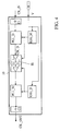
- the display system 1 also comprises a transmission circuit of the clock signal 10 that receives an input clock signal CK_IN coming from the graphics card 5, and supplies, towards an input of the digital transmitter 6, an output clock signal CK_OUT.
- the digital transmitter 6 receives the data D5 at a certain clock frequency, in the case illustrated as an example above 40 MHz.
- the display system 1 comprises an alarm device 9, capable of receiving an external alarm signal, in particular a notification of an alarm situation AL_0.
- Such an alarm device 9 is connected to the transmission circuit of the clock signal 10 and is able to send an alarm signal V to it.
- the transmission circuit of the clock signal 10 is in particular able to prevent the passage of the clock signal between an upstream device or stage, in particular the graphics card 5, and a downstream device or stage, in particular the digital transmitter 6, inhibiting the output and interrupting the supply of the output clock signal CK_OUT: in this case, the graphics card 5 continues to transmit the data D5 with the correct input clock signal CK_IN, but the digital transmitter 6 receives in input an output clock signal CK_OUT that is constantly zero and thus stops sending data D6 representative of the data D4 sent by the microprocessor 4. The result is that the screen 8A stops transmitting interpretable data, so as to display to an operator that an alarm has occurred.
- the transmission circuit of the clock signal 10 comprises:
- the transmission circuit of the clock signal 10 comprises at least:
- the transmission circuit of the clock signal 10 also comprises isolation means, in particular a first and a second condenser C1 and C2 (for example of class Y2) respectively connected to the first and second PLL components and to the input and output terminals of the transmission circuit of the clock signal 10, as well as a further isolation means, in particular a digital isolator IS (for example an AduM110), of the transformer type, inserted between the two PLL components.
- isolation means in particular a first and a second condenser C1 and C2 (for example of class Y2) respectively connected to the first and second PLL components and to the input and output terminals of the transmission circuit of the clock signal 10, as well as a further isolation means, in particular a digital isolator IS (for example an AduM110), of the transformer type, inserted between the two PLL components.
- a digital isolator IS for example an AduM110
- the transmission circuit of the clock signal 10 comprises, starting from the first input terminal CK_IN, the cascade of the first condenser C1, of the first component PLL_D, of the digital isolator IS, of the second component PLL_M and of the second condenser C1, in turn connected to the output terminal CK_OUT.
- the transmission circuit of the clock signal 10 also comprises a first and a second linear regulator, REG_M and REG_D, connected to the second input terminal V and able to supply power to the two PLL components and the digital isolator IS.
- a first and a second linear regulator REG_M and REG_D
- REG_M and REG_D linear regulators
- such linear regulators can be models LP38691-ADJ produced by National Semiconductor.
- the two linear regulators REG_M and REG_D are power supplied rightly from the alarm signal V and therefore:
- figure 5 schematically illustrates the patterns of the various clock signals within the transmission circuit of the clock signal 10 (the delays imposed by the various components, for example by the condensers, are of no importance here, and therefore are illustrated purely for indicating purposes).
- it illustrates:
- the two PLL components neutralise one another the modifications made to the frequency of the clock signal that propagates in the transmission circuit of the clock signal 10.
- Figure 6 again illustrating the patterns of the clock signals CK_IN, CK_D and CK_OUT within the transmission circuit of the clock signal 10, on the other hand, shows how such a transmission circuit works in the presence of an alarm signal.
- the alarm signal V is cancelled at a certain moment in time and the output clock signal CK_OUT is constantly zero from such a moment in time.
- figures 7 and 8 again illustrating the patterns of the clock signals CK_IN, CK_D and CK_OUT, show the operation of the transmission circuit of the clock signal 10 in the case of short-circuit of one of the two components PLL_D or PLL_M, respectively.
- the transmission circuit of the clock signal 10 in the case of a short-circuit of the second component PLL_M, operates like in figure 7 .
- the frequency of the output clock signal CK_OUT is halved, the second component PLL_M not indeed compensating for the modifications or variations in frequency introduced by the first component PLL_D.
- the transmission circuit of the clock signal 10 in the case of a short-circuit of the first component PLL_D, operates like in figure 8 .
- the frequency of the output clock signal CK_OUT is doubled, since the halving carried out by the first component PLL_D is missing.
- the digital transmitter 6 still receives data D5 in output from the graphics card 5, but with an incorrect clock frequency value, which translates into the loss of the display data: this is actually an optimal situation, because it allows the transmission of incorrect display data to be prevented, under all circumstances in the presence of failures.
- a display system of critical data from the safety point of view in the form of synchronous digital signals transmitted through a synchronous transmission channel comprising at least:
- the system comprises at least one transmission circuit 10 as described above for transmitting a clock signal, such a circuit being inserted between two consecutive intermediate devices, in particular the graphics card 5 and the digital transmitter 6, and being controlled by the external alarm signal V received from the alarm device 9 in turn receiving notification of an alarm situation AL-0.
- the external alarm signal V drives the transmission circuit 10 to block the transmission of the clock signal and the consequent displaying of the critical data in an alarm situation.
- the digital isolator IS generally requires a sufficiently low frequency: advantageously, according to an aspect of the present invention, the fact that the first component PLL_D, which divides the frequency of the input clock signal CK_IN, is upstream of such a digital isolator IS, allows the occurrence of distortions to be reduced.
- a digital isolator IS of the transformer type with better performance than opto-isolators, which are slow, is used.
- the presence of the condensers C 1 and C2 ensures the isolation of the PLL components, in particular it ensures that it is impossible to have different energy sources to the voltage due to the alarm signal V.
- the method for transmitting synchronous digital data allows the transmission of synchronous digital data (D5), from an upstream stage 5 to a downstream stage 6 in the presence of a clock signal at a predetermined frequency.
- the invention allows good protection from latent failures, making them immediately visible, and making them look, in practice, as external alarms.
- the alarm device 9 could be integrated in the microprocessor 4.
- a display system could be made in which the upstream device or stage is the microprocessor and the downstream device or stage is the graphics card.
- a system 100 for transmitting synchronous digital signals comprising an upstream device 5 connected for the transmission of synchronous digital data D5 to a downstream device 6,
- the present invention thus provides a transmission circuit of the clock signal, a display system of critical data and a relative method able to enhance the level of safety of a transmission system of critical data from the safety point of view, in particular for use in vital systems, so as to obtain a fail-silent type behaviour and able to allow the detection of internal failures, and to prevent the generation of latent failures, in this way overcoming the drawbacks highlighted in relation to known devices and methods.
- the transmission circuit of the clock signal thanks to the presence of the PLL components, in the absence of the alarm signal V, neutralises the modifications made to the frequency of the clock signal that propagates, whereas, in the presence of the alarm signal V, it prevents the passage of the clock signal, in this way ensuring that incorrect information is not transmitted, for example shown to an operator.
- the two components are no longer able to neutralise one another the modifications made to the frequency of the clock signal, and thus to the downstream device is sent a clock signal with a different frequency value to a nominal frequency, so as to prevent the display system from reading the signals, and consequently preventing the transmission of incorrect information.
- the transmission circuit and the method according to the present invention thus allow a good protection from latent failures, making them immediately visible, and making them look, in practice, as external alarms.
- a failure in one of the PLL components and therefore in the frequency variations applied by them results in an output clock signal being received with a different frequency value to an expected value and consequent detection of the failure itself.
- the transmission circuit of the clock signal comprises upstream and downstream isolators, preferably made from isolation condensers, and a digital isolator of the transformer type, capable of decoupling the first and second PLL components.
- upstream and downstream isolators preferably made from isolation condensers
- a digital isolator of the transformer type capable of decoupling the first and second PLL components.
Landscapes
- Engineering & Computer Science (AREA)
- Computer Networks & Wireless Communication (AREA)
- Signal Processing (AREA)
- Synchronisation In Digital Transmission Systems (AREA)
- Reduction Or Emphasis Of Bandwidth Of Signals (AREA)
- Communication Control (AREA)
Claims (13)
- Übertragungsschaltung (10) eines Taktsignals zur Übertragung synchroner digitaler Signale (D5) zwischen einem vorgelagerten Element (5) und einem nachgelagerten Element (6), die durch die Schaltung (10) verbunden sind, die einen ersten Eingangsanschluss, der mit einem Ausgangsanschluss des vorgelagerten Elements (5) verbunden ist und von diesem ein Eingangstaktsignal (CK_IN) mit einer vorgegebenen Frequenz empfängt, und einen Ausgangsanschluss, der mit einem Eingangsanschluss des nachgelagerten Elements (6) verbunden ist und dieses mit einem Ausgangstaktsignal (CK_OUT) mit einer vorgegebenen Frequenz versorgt, und auch einen zweiten Eingangsanschluss, der ein Alarmsignal (V) von einem externen Element (9) empfängt, aufweist, wobei die Schaltung (10) dadurch gekennzeichnet ist, dass sie mindestens umfasst:- ein erstes Bauteil (PLL_D), das so aufgebaut ist, dass es einen Frequenzwert des Eingangstaktsignals (CK_IN) modifiziert und ein Zwischentaktsignal (CK_D) bereitstellt, und- ein zweites Bauteil (PLL_M), das so aufgebaut ist, dass es einen Frequenzwert des Zwischentaktsignals (CK_D) modifiziert,wobei die ersten und zweiten Bauteile (PLL_D, PLL_M) zwischen dem ersten Eingangsanschluss und dem Ausgangsanschluss miteinander in einer Kaskadenschaltung verbunden sind und mit dem zweiten Eingangsanschluss verbunden sind, um:- in Abwesenheit des externen Alarmsignals (V) gegenseitig die den Taktsignalen auferlegten Modifikationen zu neutralisieren, und- in Anwesenheit des externen Alarmsignals (V) den Durchgang des Taktsignals zu verhindern,wobei im Fall des Versagens eines der ersten und zweiten Bauteile (PLL_D, PLL_M) das nachgelagerte Element (6) ein Taktsignal mit einem von einer Nennfrequenz verschiedenen Frequenzwert empfängt.
- Übertragungsschaltung nach Anspruch 1, dadurch gekennzeichnet, dass die ersten und zweiten Bauteile (PLL_D, PLL_M) Phasenregelkreise sind, die in der Lage sind, die Frequenz eines Eingangssignals zu dividieren beziehungsweise zu multiplizieren.
- Übertragungsschaltung nach Anspruch 2, dadurch gekennzeichnet, dass die ersten und zweiten Bauteile (PLL_D, PLL_M) mit demselben vorgegebenen Koeffizienten teilen beziehungsweise multiplizieren.
- Übertragungsschaltung nach Anspruch 1, dadurch gekennzeichnet, dass diese ein zwischen den ersten Eingangsanschluss (CK_IN) und das erste Bauteil (PLL_D) eingebrachtes Isoliermittel (C1) umfasst.
- Übertragungsschaltung nach Anspruch 1, dadurch gekennzeichnet, dass diese ein zwischen das zweite Bauteil (PLL_M) und den Ausgangsanschluss (CK_OUT) eingebrachtes Isoliermittel (C2) umfasst.
- Übertragungsschaltung nach Anspruch 4 oder 5, dadurch gekennzeichnet, dass das Isoliermittel (C1, C2) ein Kondensator ist.
- Übertragungsschaltung nach einem der vorherigen Ansprüche, dadurch gekennzeichnet, dass diese ein zwischen die ersten und zweiten Bauteile (PLL_D, PLL_M) eingebrachtes weiteres Isoliermittel (IS) umfasst.
- Übertragungsschaltung nach Anspruch 7, dadurch gekennzeichnet, dass das weitere Isoliermittel (IS) einen digitalen Isolator, vorzugsweise nach Art eines Kondensators, umfasst.
- Übertragungsschaltung nach einem der vorherigen Ansprüche, dadurch gekennzeichnet, dass diese auch mindestens einen ersten und einen zweiten Linearregler (REG_M, REG_D) umfasst, die mit dem zweiten Eingangsanschluss (V) und den ersten und zweiten Bauteilen (PLL_D, PLL_M) verbunden sind.
- Übertragungsschaltung nach Anspruch 9, wenn dieser abhängig von Anspruch 7 ist, dadurch gekennzeichnet, dass die ersten und zweiten Linearregler (REG_M, REG_D) mit dem weiteren isoliermittel (IS) verbunden sind.
- Übertragungsschaltung nach einem der vorherigen Ansprüche, dadurch gekennzeichnet, dass der zweite Eingangsanschluss (V) ein Spannungsalarmsignal empfängt, das im Normalfall einen Wert aufweist, der identisch ist mit einem Energieversorgungsspannungswert der ersten und zweiten Bauteile (PLL_D, PLL_M), und im Alarmfall einen Wert von Null aufweist, der in der Lage ist, die Energieversorgung der ersten und zweiten Bauteile (PLL_D, PLL_M) zu stoppen, um den Durchgang des Taktsignals von dem vorgelagerten Element (5) zu dem nachgelagerten Element (6) zu verhindern.
- Anzeigesystem von aus Sicherheitssicht kritischen Daten in Form von synchronen digitalen Signalen, die durch einen synchronen Übertragungskanal übertragen werden, umfassend mindestens:- einen zum Empfang von externen Daten (D0) an einem Eingangsanschluss geeigneten Mikroprozessor (4),- einen zur Anzeige der kritischen Daten an einem Bildschirm (8A) geeigneten Monitor (3), und- eine Vielzahl von Zwischenelementen (5, 6, 7, 8), die zwischen dem Mikroprozessor (4) und dem Bildschirm (8A) miteinander in einer Kaskadenschaltung verbunden sind, dadurch gekennzeichnet, dass dieses mindestens eine Übertragungsschaltung (10) nach einem der vorherigen Ansprüche zur Übertragung eines Taktsignals (CK_IN, CK_OUT) umfasst, wobei die Schaltung zwischen zwei aufeinanderfolgenden Zwischenelementen (5, 6, 7, 8) in die Kaskadenschaltung eingebracht ist und von einem empfangenen externen Alarmsignal (V) eines Alarmelements (9) gesteuert wird, das wiederum die Benachrichtigung über eine Alarmsituation (AL_O) empfängt, wobei das externe Alarmsignal (V) die Übertragungsschaltung (10) zum Blockieren der Übertragung des Taktsignals und zur folgerichtigen Anzeige der kritischen Daten in einem Alarmzustand steuert.
- Verfahren zur Übertragung synchroner digitaler Daten zwischen einem vorgelagerten Abschnitt (5) und einem nachgelagerten Abschnitt (6) in der Anwesenheit eines Taktsignals mit einer vorgegebenen Frequenz, wobei das Verfahren nacheinander die folgenden Schritte vorsieht:- Aufnehmen und Übertragen eines Eingangstaktsignals (CK_IN) von dem vorgelagerten Abschnitt (5) zu einer Übertragungsschaltung (10),- erste Frequenzvariation des Eingangstaktsignals (CK_IN) und Generieren eines Zwischentaktsignals (CK_D),- zweite Frequenzvariation des Zwischentaktsignals (CK_D) und Generieren eines Ausgangstaktsignals (CK_OUT) und- Empfang des zweiten Taktsignals (CK_OUT) durch den nachgelagerten Abschnitt (6),wobei die ersten und zweiten Frequenzvariationen durchgeführt werden, um:- sich in Abwesenheit eines externen Alarmsignals (V) gegenseitig zu neutralisieren,- in Anwesenheit des externen Alarmsignals (V) den Durchgang des Taktsignals (CK_IN, CK_OUT) zu verhindern,wobei ein Fehler in einem der ersten und zweiten Frequenzvariationen dazu führt, dass mit der Detektion des Fehlers der nachgelagerte Abschnitt (6) das Ausgangstaktsignal mit einem von einem erwarteten Wert verschiedenen Frequenzwert empfängt.
Applications Claiming Priority (1)
| Application Number | Priority Date | Filing Date | Title |
|---|---|---|---|
| IT000247A ITMI20080247A1 (it) | 2008-02-18 | 2008-02-18 | Circuito di trasmissione di un segnale di clock per la trasmissione di segnali digitali sincroni. |
Publications (3)
| Publication Number | Publication Date |
|---|---|
| EP2099153A2 EP2099153A2 (de) | 2009-09-09 |
| EP2099153A3 EP2099153A3 (de) | 2010-06-30 |
| EP2099153B1 true EP2099153B1 (de) | 2011-08-10 |
Family
ID=40291656
Family Applications (1)
| Application Number | Title | Priority Date | Filing Date |
|---|---|---|---|
| EP09153117A Not-in-force EP2099153B1 (de) | 2008-02-18 | 2009-02-18 | Taktsignal-Übertragungsschaltung zur Übertragung synchroner digitaler Signale |
Country Status (3)
| Country | Link |
|---|---|
| EP (1) | EP2099153B1 (de) |
| AT (1) | ATE520216T1 (de) |
| IT (1) | ITMI20080247A1 (de) |
Family Cites Families (5)
| Publication number | Priority date | Publication date | Assignee | Title |
|---|---|---|---|---|
| US4868826A (en) * | 1987-08-31 | 1989-09-19 | Triplex | Fault-tolerant output circuits |
| DE10249592A1 (de) * | 2002-10-24 | 2004-06-17 | Abb Research Ltd. | Datenverarbeitungsknoten für ein Leitsystem |
| US6842056B1 (en) * | 2003-06-24 | 2005-01-11 | Intel Corporation | Cascaded phase-locked loops |
| US20060001494A1 (en) * | 2004-07-02 | 2006-01-05 | Bruno Garlepp | Cascaded locked-loop circuits deriving high-frequency, low noise clock signals from a jittery, low-frequency reference |
| JP2006059100A (ja) * | 2004-08-19 | 2006-03-02 | Ricoh Co Ltd | シリアル通信システム装置 |
-
2008
- 2008-02-18 IT IT000247A patent/ITMI20080247A1/it unknown
-
2009
- 2009-02-18 AT AT09153117T patent/ATE520216T1/de not_active IP Right Cessation
- 2009-02-18 EP EP09153117A patent/EP2099153B1/de not_active Not-in-force
Also Published As
| Publication number | Publication date |
|---|---|
| ATE520216T1 (de) | 2011-08-15 |
| ITMI20080247A1 (it) | 2009-08-19 |
| EP2099153A2 (de) | 2009-09-09 |
| EP2099153A3 (de) | 2010-06-30 |
Similar Documents
| Publication | Publication Date | Title |
|---|---|---|
| EP1892872A2 (de) | Fehlerprüfung für Datenübertragung zwischen einer Leitstation und einer Folgestation | |
| EP1237282B1 (de) | Schaltung zur Detektion von Störungen der Periodendauer in einem Taktsignal | |
| CN107480016B (zh) | 一种传输设备接口电路自检方法及其电路自检系统 | |
| EP2823404B1 (de) | Kollisionsdetektion in eia-485 bus-systemen | |
| US8995471B2 (en) | Shelf of a network synchronization device, and network synchronization device | |
| EP2099153A2 (de) | Taktsignal-Übertragungsschaltung zur Übertragung synchroner digitaler Signale | |
| EP0228213B1 (de) | System für das Übertragen und Empfangen von asynchronen Paralleldaten von nichthomogener variabler Breite über ein synchrones Serienübertragungsmittel mit hoher Informationsgeschwindigkeit | |
| EP1837672B1 (de) | Verfahren und Vorrichtung zur Fehlerdetektion | |
| US20160301521A1 (en) | Control system | |
| KR100380658B1 (ko) | 삼중화 제어장치의 직렬통신을 이용한 출력장치와 그제어방법 | |
| US20130054676A1 (en) | Computer network based hazardous condition monitoring system and server | |
| US6016559A (en) | Multifunctional intergrated electronic product and method for preventing operation failure of the same | |
| KR100328475B1 (ko) | 직렬데이타통신시스템에서통신선로의이중화장치와그방법 | |
| US5736889A (en) | Duplexing control apparatus for use in a time division switching device | |
| CN111587551A (zh) | 基于冗余的信息产生数据流的系统 | |
| JPH10313349A (ja) | データ通信装置 | |
| JP2003248633A (ja) | 耐障害性環境でバイナリ信号の状態を符号化/復号する方法 | |
| JPS61216541A (ja) | デ−タ伝送装置 | |
| JP2816746B2 (ja) | シリアルデータ伝送システム | |
| KR100369685B1 (ko) | 교환기의 기준클럭 동기 장치 및 그 방법 | |
| JP2538682B2 (ja) | 基準クロック源自動切替え方式 | |
| JP2596318B2 (ja) | 伝送装置 | |
| KR200403626Y1 (ko) | 통신 시스템의 이중화 제어장치 | |
| JP5664540B2 (ja) | 監視回路、マイクロコンピュータ及び通信システム | |
| KR100247033B1 (ko) | 동기식 전송시스템에서 데이터 통신 채널의 클럭 장애 검출 및 보상장치 |
Legal Events
| Date | Code | Title | Description |
|---|---|---|---|
| PUAI | Public reference made under article 153(3) epc to a published international application that has entered the european phase |
Free format text: ORIGINAL CODE: 0009012 |
|
| AK | Designated contracting states |
Kind code of ref document: A2 Designated state(s): AT BE BG CH CY CZ DE DK EE ES FI FR GB GR HR HU IE IS IT LI LT LU LV MC MK MT NL NO PL PT RO SE SI SK TR |
|
| AX | Request for extension of the european patent |
Extension state: AL BA RS |
|
| PUAL | Search report despatched |
Free format text: ORIGINAL CODE: 0009013 |
|
| AK | Designated contracting states |
Kind code of ref document: A3 Designated state(s): AT BE BG CH CY CZ DE DK EE ES FI FR GB GR HR HU IE IS IT LI LT LU LV MC MK MT NL NO PL PT RO SE SI SK TR |
|
| AX | Request for extension of the european patent |
Extension state: AL BA RS |
|
| RIC1 | Information provided on ipc code assigned before grant |
Ipc: G06F 11/00 20060101ALI20100525BHEP Ipc: H04L 7/00 20060101AFI20090729BHEP Ipc: H04L 25/02 20060101ALN20100525BHEP |
|
| GRAP | Despatch of communication of intention to grant a patent |
Free format text: ORIGINAL CODE: EPIDOSNIGR1 |
|
| 17P | Request for examination filed |
Effective date: 20101228 |
|
| RIC1 | Information provided on ipc code assigned before grant |
Ipc: H04L 7/00 20060101AFI20110124BHEP Ipc: H04L 25/02 20060101ALN20110124BHEP Ipc: G06F 11/00 20060101ALI20110124BHEP |
|
| AKX | Designation fees paid |
Designated state(s): AT BE BG CH CY CZ DE DK EE ES FI FR GB GR HR HU IE IS IT LI LT LU LV MC MK MT NL NO PL PT RO SE SI SK TR |
|
| GRAS | Grant fee paid |
Free format text: ORIGINAL CODE: EPIDOSNIGR3 |
|
| GRAA | (expected) grant |
Free format text: ORIGINAL CODE: 0009210 |
|
| AK | Designated contracting states |
Kind code of ref document: B1 Designated state(s): AT BE BG CH CY CZ DE DK EE ES FI FR GB GR HR HU IE IS IT LI LT LU LV MC MK MT NL NO PL PT RO SE SI SK TR |
|
| REG | Reference to a national code |
Ref country code: GB Ref legal event code: FG4D |
|
| REG | Reference to a national code |
Ref country code: CH Ref legal event code: EP |
|
| REG | Reference to a national code |
Ref country code: IE Ref legal event code: FG4D |
|
| REG | Reference to a national code |
Ref country code: DE Ref legal event code: R096 Ref document number: 602009002043 Country of ref document: DE Effective date: 20111006 |
|
| REG | Reference to a national code |
Ref country code: NL Ref legal event code: VDEP Effective date: 20110810 |
|
| LTIE | Lt: invalidation of european patent or patent extension |
Effective date: 20110810 |
|
| PG25 | Lapsed in a contracting state [announced via postgrant information from national office to epo] |
Ref country code: HR Free format text: LAPSE BECAUSE OF FAILURE TO SUBMIT A TRANSLATION OF THE DESCRIPTION OR TO PAY THE FEE WITHIN THE PRESCRIBED TIME-LIMIT Effective date: 20110810 Ref country code: FI Free format text: LAPSE BECAUSE OF FAILURE TO SUBMIT A TRANSLATION OF THE DESCRIPTION OR TO PAY THE FEE WITHIN THE PRESCRIBED TIME-LIMIT Effective date: 20110810 Ref country code: NO Free format text: LAPSE BECAUSE OF FAILURE TO SUBMIT A TRANSLATION OF THE DESCRIPTION OR TO PAY THE FEE WITHIN THE PRESCRIBED TIME-LIMIT Effective date: 20111110 Ref country code: NL Free format text: LAPSE BECAUSE OF FAILURE TO SUBMIT A TRANSLATION OF THE DESCRIPTION OR TO PAY THE FEE WITHIN THE PRESCRIBED TIME-LIMIT Effective date: 20110810 Ref country code: PT Free format text: LAPSE BECAUSE OF FAILURE TO SUBMIT A TRANSLATION OF THE DESCRIPTION OR TO PAY THE FEE WITHIN THE PRESCRIBED TIME-LIMIT Effective date: 20111212 Ref country code: SE Free format text: LAPSE BECAUSE OF FAILURE TO SUBMIT A TRANSLATION OF THE DESCRIPTION OR TO PAY THE FEE WITHIN THE PRESCRIBED TIME-LIMIT Effective date: 20110810 Ref country code: IS Free format text: LAPSE BECAUSE OF FAILURE TO SUBMIT A TRANSLATION OF THE DESCRIPTION OR TO PAY THE FEE WITHIN THE PRESCRIBED TIME-LIMIT Effective date: 20111210 Ref country code: LT Free format text: LAPSE BECAUSE OF FAILURE TO SUBMIT A TRANSLATION OF THE DESCRIPTION OR TO PAY THE FEE WITHIN THE PRESCRIBED TIME-LIMIT Effective date: 20110810 |
|
| REG | Reference to a national code |
Ref country code: AT Ref legal event code: MK05 Ref document number: 520216 Country of ref document: AT Kind code of ref document: T Effective date: 20110810 |
|
| PG25 | Lapsed in a contracting state [announced via postgrant information from national office to epo] |
Ref country code: GR Free format text: LAPSE BECAUSE OF FAILURE TO SUBMIT A TRANSLATION OF THE DESCRIPTION OR TO PAY THE FEE WITHIN THE PRESCRIBED TIME-LIMIT Effective date: 20111111 Ref country code: AT Free format text: LAPSE BECAUSE OF FAILURE TO SUBMIT A TRANSLATION OF THE DESCRIPTION OR TO PAY THE FEE WITHIN THE PRESCRIBED TIME-LIMIT Effective date: 20110810 Ref country code: SI Free format text: LAPSE BECAUSE OF FAILURE TO SUBMIT A TRANSLATION OF THE DESCRIPTION OR TO PAY THE FEE WITHIN THE PRESCRIBED TIME-LIMIT Effective date: 20110810 Ref country code: LV Free format text: LAPSE BECAUSE OF FAILURE TO SUBMIT A TRANSLATION OF THE DESCRIPTION OR TO PAY THE FEE WITHIN THE PRESCRIBED TIME-LIMIT Effective date: 20110810 Ref country code: CY Free format text: LAPSE BECAUSE OF FAILURE TO SUBMIT A TRANSLATION OF THE DESCRIPTION OR TO PAY THE FEE WITHIN THE PRESCRIBED TIME-LIMIT Effective date: 20110810 Ref country code: PL Free format text: LAPSE BECAUSE OF FAILURE TO SUBMIT A TRANSLATION OF THE DESCRIPTION OR TO PAY THE FEE WITHIN THE PRESCRIBED TIME-LIMIT Effective date: 20110810 |
|
| PG25 | Lapsed in a contracting state [announced via postgrant information from national office to epo] |
Ref country code: BE Free format text: LAPSE BECAUSE OF FAILURE TO SUBMIT A TRANSLATION OF THE DESCRIPTION OR TO PAY THE FEE WITHIN THE PRESCRIBED TIME-LIMIT Effective date: 20110810 |
|
| PG25 | Lapsed in a contracting state [announced via postgrant information from national office to epo] |
Ref country code: CZ Free format text: LAPSE BECAUSE OF FAILURE TO SUBMIT A TRANSLATION OF THE DESCRIPTION OR TO PAY THE FEE WITHIN THE PRESCRIBED TIME-LIMIT Effective date: 20110810 Ref country code: SK Free format text: LAPSE BECAUSE OF FAILURE TO SUBMIT A TRANSLATION OF THE DESCRIPTION OR TO PAY THE FEE WITHIN THE PRESCRIBED TIME-LIMIT Effective date: 20110810 |
|
| PGFP | Annual fee paid to national office [announced via postgrant information from national office to epo] |
Ref country code: FR Payment date: 20120217 Year of fee payment: 4 |
|
| PG25 | Lapsed in a contracting state [announced via postgrant information from national office to epo] |
Ref country code: RO Free format text: LAPSE BECAUSE OF FAILURE TO SUBMIT A TRANSLATION OF THE DESCRIPTION OR TO PAY THE FEE WITHIN THE PRESCRIBED TIME-LIMIT Effective date: 20110810 Ref country code: EE Free format text: LAPSE BECAUSE OF FAILURE TO SUBMIT A TRANSLATION OF THE DESCRIPTION OR TO PAY THE FEE WITHIN THE PRESCRIBED TIME-LIMIT Effective date: 20110810 |
|
| PGFP | Annual fee paid to national office [announced via postgrant information from national office to epo] |
Ref country code: DE Payment date: 20120119 Year of fee payment: 4 |
|
| PLBE | No opposition filed within time limit |
Free format text: ORIGINAL CODE: 0009261 |
|
| STAA | Information on the status of an ep patent application or granted ep patent |
Free format text: STATUS: NO OPPOSITION FILED WITHIN TIME LIMIT |
|
| PG25 | Lapsed in a contracting state [announced via postgrant information from national office to epo] |
Ref country code: DK Free format text: LAPSE BECAUSE OF FAILURE TO SUBMIT A TRANSLATION OF THE DESCRIPTION OR TO PAY THE FEE WITHIN THE PRESCRIBED TIME-LIMIT Effective date: 20110810 |
|
| PGFP | Annual fee paid to national office [announced via postgrant information from national office to epo] |
Ref country code: IT Payment date: 20120228 Year of fee payment: 4 |
|
| 26N | No opposition filed |
Effective date: 20120511 |
|
| REG | Reference to a national code |
Ref country code: DE Ref legal event code: R097 Ref document number: 602009002043 Country of ref document: DE Effective date: 20120511 |
|
| PG25 | Lapsed in a contracting state [announced via postgrant information from national office to epo] |
Ref country code: MC Free format text: LAPSE BECAUSE OF NON-PAYMENT OF DUE FEES Effective date: 20120229 |
|
| REG | Reference to a national code |
Ref country code: IE Ref legal event code: MM4A |
|
| PG25 | Lapsed in a contracting state [announced via postgrant information from national office to epo] |
Ref country code: IE Free format text: LAPSE BECAUSE OF NON-PAYMENT OF DUE FEES Effective date: 20120218 |
|
| PG25 | Lapsed in a contracting state [announced via postgrant information from national office to epo] |
Ref country code: MK Free format text: LAPSE BECAUSE OF FAILURE TO SUBMIT A TRANSLATION OF THE DESCRIPTION OR TO PAY THE FEE WITHIN THE PRESCRIBED TIME-LIMIT Effective date: 20110810 |
|
| PG25 | Lapsed in a contracting state [announced via postgrant information from national office to epo] |
Ref country code: ES Free format text: LAPSE BECAUSE OF FAILURE TO SUBMIT A TRANSLATION OF THE DESCRIPTION OR TO PAY THE FEE WITHIN THE PRESCRIBED TIME-LIMIT Effective date: 20111121 |
|
| PG25 | Lapsed in a contracting state [announced via postgrant information from national office to epo] |
Ref country code: BG Free format text: LAPSE BECAUSE OF FAILURE TO SUBMIT A TRANSLATION OF THE DESCRIPTION OR TO PAY THE FEE WITHIN THE PRESCRIBED TIME-LIMIT Effective date: 20111110 |
|
| PG25 | Lapsed in a contracting state [announced via postgrant information from national office to epo] |
Ref country code: MT Free format text: LAPSE BECAUSE OF FAILURE TO SUBMIT A TRANSLATION OF THE DESCRIPTION OR TO PAY THE FEE WITHIN THE PRESCRIBED TIME-LIMIT Effective date: 20110810 |
|
| REG | Reference to a national code |
Ref country code: CH Ref legal event code: PL |
|
| GBPC | Gb: european patent ceased through non-payment of renewal fee |
Effective date: 20130218 |
|
| PG25 | Lapsed in a contracting state [announced via postgrant information from national office to epo] |
Ref country code: CH Free format text: LAPSE BECAUSE OF NON-PAYMENT OF DUE FEES Effective date: 20130228 Ref country code: DE Free format text: LAPSE BECAUSE OF NON-PAYMENT OF DUE FEES Effective date: 20130903 Ref country code: LI Free format text: LAPSE BECAUSE OF NON-PAYMENT OF DUE FEES Effective date: 20130228 |
|
| REG | Reference to a national code |
Ref country code: FR Ref legal event code: ST Effective date: 20131031 |
|
| REG | Reference to a national code |
Ref country code: DE Ref legal event code: R119 Ref document number: 602009002043 Country of ref document: DE Effective date: 20130903 |
|
| PG25 | Lapsed in a contracting state [announced via postgrant information from national office to epo] |
Ref country code: IT Free format text: LAPSE BECAUSE OF NON-PAYMENT OF DUE FEES Effective date: 20130218 |
|
| PG25 | Lapsed in a contracting state [announced via postgrant information from national office to epo] |
Ref country code: FR Free format text: LAPSE BECAUSE OF NON-PAYMENT OF DUE FEES Effective date: 20130228 Ref country code: GB Free format text: LAPSE BECAUSE OF NON-PAYMENT OF DUE FEES Effective date: 20130218 |
|
| PG25 | Lapsed in a contracting state [announced via postgrant information from national office to epo] |
Ref country code: TR Free format text: LAPSE BECAUSE OF FAILURE TO SUBMIT A TRANSLATION OF THE DESCRIPTION OR TO PAY THE FEE WITHIN THE PRESCRIBED TIME-LIMIT Effective date: 20110810 |
|
| PG25 | Lapsed in a contracting state [announced via postgrant information from national office to epo] |
Ref country code: LU Free format text: LAPSE BECAUSE OF NON-PAYMENT OF DUE FEES Effective date: 20120218 |
|
| PG25 | Lapsed in a contracting state [announced via postgrant information from national office to epo] |
Ref country code: HU Free format text: LAPSE BECAUSE OF FAILURE TO SUBMIT A TRANSLATION OF THE DESCRIPTION OR TO PAY THE FEE WITHIN THE PRESCRIBED TIME-LIMIT Effective date: 20090218 |