EP2092563B1 - Semiconductor photodetector and radiation detecting apparatus - Google Patents
Semiconductor photodetector and radiation detecting apparatus Download PDFInfo
- Publication number
- EP2092563B1 EP2092563B1 EP07850321.6A EP07850321A EP2092563B1 EP 2092563 B1 EP2092563 B1 EP 2092563B1 EP 07850321 A EP07850321 A EP 07850321A EP 2092563 B1 EP2092563 B1 EP 2092563B1
- Authority
- EP
- European Patent Office
- Prior art keywords
- carrier capturing
- regions
- region
- photodiodes
- semiconductor
- Prior art date
- Legal status (The legal status is an assumption and is not a legal conclusion. Google has not performed a legal analysis and makes no representation as to the accuracy of the status listed.)
- Not-in-force
Links
- 239000004065 semiconductor Substances 0.000 title claims description 135
- 230000005855 radiation Effects 0.000 title claims description 24
- 239000000758 substrate Substances 0.000 claims description 72
- 239000012535 impurity Substances 0.000 claims description 26
- 230000006335 response to radiation Effects 0.000 claims description 4
- 239000000969 carrier Substances 0.000 description 32
- 238000010586 diagram Methods 0.000 description 18
- 206010034972 Photosensitivity reaction Diseases 0.000 description 15
- 230000036211 photosensitivity Effects 0.000 description 15
- 239000004020 conductor Substances 0.000 description 13
- 230000000694 effects Effects 0.000 description 8
- 238000001514 detection method Methods 0.000 description 7
- 230000035945 sensitivity Effects 0.000 description 7
- 230000009467 reduction Effects 0.000 description 6
- 230000005012 migration Effects 0.000 description 5
- 238000013508 migration Methods 0.000 description 5
- 229910052782 aluminium Inorganic materials 0.000 description 4
- XAGFODPZIPBFFR-UHFFFAOYSA-N aluminium Chemical compound [Al] XAGFODPZIPBFFR-UHFFFAOYSA-N 0.000 description 4
- 229910052737 gold Inorganic materials 0.000 description 4
- 229910052759 nickel Inorganic materials 0.000 description 4
- 238000007747 plating Methods 0.000 description 4
- 229910000679 solder Inorganic materials 0.000 description 4
- 238000010521 absorption reaction Methods 0.000 description 3
- 230000000452 restraining effect Effects 0.000 description 3
- XUIMIQQOPSSXEZ-UHFFFAOYSA-N Silicon Chemical compound [Si] XUIMIQQOPSSXEZ-UHFFFAOYSA-N 0.000 description 2
- 238000003491 array Methods 0.000 description 2
- 230000015556 catabolic process Effects 0.000 description 2
- 230000008859 change Effects 0.000 description 2
- 238000000605 extraction Methods 0.000 description 2
- 238000000034 method Methods 0.000 description 2
- 230000008569 process Effects 0.000 description 2
- 229910052710 silicon Inorganic materials 0.000 description 2
- 239000010703 silicon Substances 0.000 description 2
- 239000004925 Acrylic resin Substances 0.000 description 1
- 229920000178 Acrylic resin Polymers 0.000 description 1
- 230000000052 comparative effect Effects 0.000 description 1
- 239000000470 constituent Substances 0.000 description 1
- 238000009792 diffusion process Methods 0.000 description 1
- 230000005684 electric field Effects 0.000 description 1
- 239000003822 epoxy resin Substances 0.000 description 1
- 238000004519 manufacturing process Methods 0.000 description 1
- 238000005259 measurement Methods 0.000 description 1
- 229910052751 metal Inorganic materials 0.000 description 1
- 239000002184 metal Substances 0.000 description 1
- 238000012986 modification Methods 0.000 description 1
- 230000004048 modification Effects 0.000 description 1
- 238000002161 passivation Methods 0.000 description 1
- 238000000059 patterning Methods 0.000 description 1
- 229920000647 polyepoxide Polymers 0.000 description 1
- 230000001105 regulatory effect Effects 0.000 description 1
- 239000011347 resin Substances 0.000 description 1
- 229920005989 resin Polymers 0.000 description 1
- 238000004904 shortening Methods 0.000 description 1
- 230000001629 suppression Effects 0.000 description 1
Images


Classifications
-
- H—ELECTRICITY
- H01—ELECTRIC ELEMENTS
- H01L—SEMICONDUCTOR DEVICES NOT COVERED BY CLASS H10
- H01L27/00—Devices consisting of a plurality of semiconductor or other solid-state components formed in or on a common substrate
- H01L27/14—Devices consisting of a plurality of semiconductor or other solid-state components formed in or on a common substrate including semiconductor components sensitive to infrared radiation, light, electromagnetic radiation of shorter wavelength or corpuscular radiation and specially adapted either for the conversion of the energy of such radiation into electrical energy or for the control of electrical energy by such radiation
- H01L27/144—Devices controlled by radiation
- H01L27/146—Imager structures
- H01L27/14601—Structural or functional details thereof
- H01L27/14603—Special geometry or disposition of pixel-elements, address-lines or gate-electrodes
-
- H—ELECTRICITY
- H01—ELECTRIC ELEMENTS
- H01L—SEMICONDUCTOR DEVICES NOT COVERED BY CLASS H10
- H01L27/00—Devices consisting of a plurality of semiconductor or other solid-state components formed in or on a common substrate
- H01L27/14—Devices consisting of a plurality of semiconductor or other solid-state components formed in or on a common substrate including semiconductor components sensitive to infrared radiation, light, electromagnetic radiation of shorter wavelength or corpuscular radiation and specially adapted either for the conversion of the energy of such radiation into electrical energy or for the control of electrical energy by such radiation
- H01L27/144—Devices controlled by radiation
- H01L27/146—Imager structures
- H01L27/14601—Structural or functional details thereof
- H01L27/1464—Back illuminated imager structures
-
- H—ELECTRICITY
- H01—ELECTRIC ELEMENTS
- H01L—SEMICONDUCTOR DEVICES NOT COVERED BY CLASS H10
- H01L27/00—Devices consisting of a plurality of semiconductor or other solid-state components formed in or on a common substrate
- H01L27/14—Devices consisting of a plurality of semiconductor or other solid-state components formed in or on a common substrate including semiconductor components sensitive to infrared radiation, light, electromagnetic radiation of shorter wavelength or corpuscular radiation and specially adapted either for the conversion of the energy of such radiation into electrical energy or for the control of electrical energy by such radiation
- H01L27/144—Devices controlled by radiation
- H01L27/146—Imager structures
- H01L27/14601—Structural or functional details thereof
- H01L27/14634—Assemblies, i.e. Hybrid structures
-
- H—ELECTRICITY
- H01—ELECTRIC ELEMENTS
- H01L—SEMICONDUCTOR DEVICES NOT COVERED BY CLASS H10
- H01L27/00—Devices consisting of a plurality of semiconductor or other solid-state components formed in or on a common substrate
- H01L27/14—Devices consisting of a plurality of semiconductor or other solid-state components formed in or on a common substrate including semiconductor components sensitive to infrared radiation, light, electromagnetic radiation of shorter wavelength or corpuscular radiation and specially adapted either for the conversion of the energy of such radiation into electrical energy or for the control of electrical energy by such radiation
- H01L27/144—Devices controlled by radiation
- H01L27/146—Imager structures
- H01L27/14643—Photodiode arrays; MOS imagers
- H01L27/14654—Blooming suppression
Definitions
- the present invention relates to a semiconductor photodetector, and to a radiation detecting apparatus comprising the semiconductor photodetector.
- the semiconductor photodetector is a backside incident type photodiode array in which a plurality of photodiodes are formed on one surface side of a semiconductor substrate, while the other surface is used as a light-incident surface (see, for example, Patent Document 1: Japanese Patent Application Laid-Open No. HI 1-74553 , and Patent Document 2: WO2005/038923 ).
- the thin layer in the Document 1 aims at eliminating scattered X-rays, and does not take account of the above-mentioned crosstalk.
- the semiconductor photodetector comprises: (1) a semiconductor substrate, one face of which is an incident surface of light to be detected; (2) a plurality of pn junction-type photodiodes formed on the side of a detecting surface that is opposite to the incident surface of the semiconductor substrate; (3) and a carrier capturing portion formed between adjacent photodiodes from among the plurality of photodiodes, on the detecting surface side of the semiconductor substrate; (4) wherein the carrier capturing portion has one or a plurality of carrier capturing regions, respectively including pn-junctions, arranged at intervals.
- a carrier capturing region including a pn junction is formed between adjacent photodiodes among the plurality of photodiodes.
- carriers generated in the vicinity of adjacent photodiodes and about to flow into adjacent photodiodes through diffusing migration are drawn from the carrier capturing region. This eliminates carriers which would flow into the adjacent photodiodes by diffusing migration, and thus can favorably restrain crosstalk from occurring between the photodiodes.
- a photodiode may fall into an electrically floating state when a certain connecting point is damaged because of an initial connection error, a temperature cycle, or the like. In this case, carriers overflowing the photodiode may flow into photodiodes thereabout, thus hindering the latter photodiodes from outputting normal signals.
- carriers which would flow into adjacent photodiodes are drawn from the carrier capturing region. This can favorably restrain carriers from flowing into the adjacent photodiodes.
- the present invention provides a radiation detecting apparatus comprising the semiconductor photodetector having the above-described constitution; and a scintillator, positioned on the incident surface side of the semiconductor substrate, for emitting light in response to radiation incident thereon.
- a radiation detecting apparatus using as a semiconductor photodetector a photodetecting element having the above-described constitution allows favorably suppressing the occurrence of crosstalk between photodiodes, as described above. Also, even when a certain photodiode falls into an electrically floating state because of a breakage of a connecting point, carriers can favorably be restrained from flowing into the adjacent photodiodes. As a result, a high resolution can be attained.
- the present invention can provide a semiconductor photodetector and a radiation detecting apparatus which can favorably restrain crosstalk from occurring.
- the present invention can provide also a semiconductor photodetector and a radiation detecting apparatus in which, even when a certain photodiode falls into an electrically floating state because of a breakage of a connecting point due to an initial connection error, a temperature cycle, etc., carriers are favorably restrained from flowing into adjacent photodiodes.
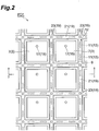
- Figs. 1 and 2 are both plan-view diagrams illustrating schematically the constitution of an embodiment of a semiconductor photodetector according to the present invention.
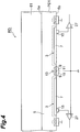
- Fig. 3 is a side-view cross-sectional diagram illustrating the cross-sectional constitution of the semiconductor photodetector taken along the line I-I in Figs. 1 and 2 .
- the constitution of a photodiode array PD1 will be described as a constitution example of a semiconductor photodetector according to the present invention.
- a first conductive type on the substrate side is taken as an n-type
- another second conductive type is taken as a p-type
- the first conductive type may be taken as a p-type
- the second conductive type as an n-type
- the photodiode array PD1 comprises a semiconductor substrate 5 one face (upper face in Fig. 3 ) of which is an incident surface 5a of light to be detected L, the other face (lower face in Fig. 3 ) being a detecting surface 5b on which the photodiodes are formed.
- Figs. 1 and 2 are plan-view diagrams where the photodiode array PD1 is viewed from the detecting surface 5b side.
- Fig. 1 illustrates a plan-view constitution of the photodiode array PD1 in which the below-described electrodes provided on the detecting surface 5b are omitted
- Fig. 2 illustrates a constitution with the electrodes present.
- the photodiode array PD1 comprises a semiconductor substrate 5, one face of which is the incident surface 5a, and plurality of pn junction-type photosensitive regions 3 formed on the detecting surface 5b side that is the opposite side to the incident surface 5a of the substrate 5.
- the semiconductor substrate 5 is an n-type (first conductive type) semiconductor substrate made of silicon (Si), and is for example a silicon substrate with a thickness of 30 to 300 ⁇ m (preferably about 100 ⁇ m) and an impurity concentration of 1 ⁇ 10 12 to 10 15 /cm 3 .
- the plurality of photosensitive regions 3 respectively including pn junctions are arranged as a two-dimensional array on the detecting surface 5b side of the semiconductor substrate 5.
- each of the photosensitive regions 3 functions as a photodiode being a photosensitive pixel that makes up the photodiode array PD1.
- a plurality of p-type (second conductive type) impurity semiconductor regions 7 are formed and arranged as a two-dimensional array on the detecting surface 5b side.
- the photosensitive regions 3 that are the photodiodes comprise pn junctions formed by the p-type regions 7 and the n-type semiconductor substrate 5.
- the p-type regions 7 are used for example p-type impurity semiconductor regions having an impurity concentration of 1 ⁇ 10 13 to 10 20 /cm 3 , and a depth of 0.05 to 20 ⁇ m (preferably about 0.2 ⁇ m).
- the carrier capturing portion 12 is formed on the detecting surface 5b side of the semiconductor substrate 5, between adjacent photosensitive regions 3 among the plurality of photosensitive regions (photodiodes) 3, i.e., between adjacent p-type regions 7.
- the carrier capturing portion 12 is constituted by the plurality of carrier capturing regions 13, comprising each a pn junction, arranged at intervals.
- the arranging directions of the carrier capturing regions 13 extending along the corresponding sides of the photosensitive regions 3, between adjacent photosensitive regions 3, are depicted in Fig. 1 by dot-dashed lines.
- the carrier capturing regions (pn junction regions) 13 comprising pn junctions are constituted thus by the pn junctions formed by the p-type regions 11 and the n-type semiconductor substrate 5.
- the p-type regions 11 are used for example p-type impurity semiconductor regions having an impurity concentration of 1 ⁇ 10 13 to 10 20 /cm 3 , and a depth of 0.05 to 20 ⁇ m (preferably about 0.2 ⁇ m).
- the carrier capturing portion 12 has two carrier capturing regions 13 arranged at intervals between a side of the photosensitive region 3 and a corresponding side of the adjacent photosensitive region 3.
- the carrier capturing portion 12 is formed, for the plurality of photosensitive regions (photodiodes) 3, in such a way that the photosensitive regions 3 are respectively surrounded by the plurality of carrier capturing regions 13 arranged at intervals, as seen from the detecting surface 5b side.
- one photosensitive region 3 as a photodiode is surrounded by a total of eight carrier capturing regions 13, with two carrier capturing regions 13 each on the left side, right side, lower side and upper side of the photosensitive region 3 depicted in Fig. 1 .
- the carrier capturing regions 13 of the carrier capturing portion 12 are arranged so as to be sandwiched between the high-concentration n-type regions 9.
- the high-concentration n-type region 9 has a function of electrically separating from each other adjacent photodiodes of the photosensitive regions 3. Providing such high-concentration n-type regions 9 allows electrically separating the adjacent photodiodes reliably, thereby lowering crosstalk between the photodiodes and regulating the breakdown voltage (reverse breakdown voltage).
- the high-concentration n-type region 9 is used for example an n-type high-concentration impurity semiconductor region having an impurity concentration of 1 ⁇ 10 13 to 10 20 /cm 3 , and a thickness of 0.1 to several tens of ⁇ m (preferably about 3 ⁇ m).
- the thickness of the high-concentration n-type region 9 is preferably larger than the depth of the p-type regions 11 that make up the carrier capturing regions 13.
- the high-concentration n-type regions 9 are formed for the respective photosensitive regions (photodiodes) 3 such that the photosensitive region 3 is surrounded by the high-concentration n-type region 9 with a continuous region pattern, as seen from the detecting surface 5b side.
- the photosensitive region 3 and the corresponding high-concentration n-type region 9 are both surrounded by the plurality of carrier capturing regions 13 arranged at intervals of the carrier capturing portion 12.
- the photosensitive regions 3 located at the edge (chip edge) of the semiconductor substrate 5 it is not necessary to form the high-concentration n-type regions 9 and the carrier capturing regions 13 of the carrier capturing portion 12 on the chip edge side, since there are no adjacent photosensitive regions 3 on the chip edge side.
- a high-concentration n-type region 9 and/or a carrier capturing region 13 may also be formed on such a chip edge side.
- a passivation film and a thermally oxidized film (not depicted) as an electrically insulating film is further formed on the detecting surface 5b that is the front surface of the semiconductor substrate 5.
- an AR film (not depicted) for protecting the incident surface 5a and suppressing reflection of light L.
- the incident surface 5a of the semiconductor substrate 5 in the photodiode array PD1 is made substantially flat as illustrated in Fig. 3 , although the incident surface 5a is not limited to such a constitution.
- the incident surface 5a is not limited to such a constitution.
- such a constitution allows shortening the distance between the incident surface 5a of the n-type semiconductor substrate 5 and the p-type regions 7 that make up the photosensitive regions 3.
- Each electrode 15 includes an electrode pad, an under-bump metal (UBM), and a bump electrode 17.
- UBM under-bump metal
- the electrode pad is made of an aluminum film, for example, and is electrically connected to the p-type region 7 through a contact hole formed in the thermally oxidized film.
- the UBM is formed, for example, by plating an electrode conductor with Ni and Au in succession.
- the bump electrode 17 is made of solder, and is formed on the UBM.
- Each electrode 19 includes an electrode conductor 21, a UBM, and a bump electrode 23.
- the UBM is not shown in the figure.
- the electrode conductor 21 is made of an aluminum film, for example, and is electrically connected to the high-concentration n-type region 9 and p-type region 11 through a contact hole formed in the thermally oxidized film. As is also illustrated in Figs. 2 and 3 , the electrode conductor 21 is formed so as to cover entirely the p-type regions 11 of the carrier capturing regions 13 as well as the high-concentration n-type regions 9 of both sides sandwiching the p-type regions 11, as seen from the detecting surface 5b side of the semiconductor substrate 5.
- the UBM is formed, for example, by plating the electrode conductor 21 with Ni and Au in succession.
- the bump electrode 23 is made of solder, and is formed on the UBM.
- the electrode 19 is connected to a reference potential (for example a ground potential).
- the anode extraction of each photodiode is realized by the electrode 15, whereas the cathode extraction is realized by the electrode 19.
- the photodiode array PD1 are formed depletion layers 25 in the respective boundaries of the pn junctions of the photosensitive regions 3 and the boundaries of the pn junctions of the carrier capturing regions 13.
- each photodiode When the light L to be detected is incident on the photodiode array PD1 from the incident surface 5a side, each photodiode generates a carrier corresponding to the incident light.
- the photocurrent from the thus generated carrier is taken out from the electrode 15 (bump electrode 17) connected to the p-type region 7 of the photosensitive region 3.
- the output from the electrode 15 is connected to the inverting input terminal of a differential amplifier 27.
- the non-inverting input terminal of the differential amplifier 27 is connected to the reference potential in common with the electrode 19.
- the photodiode array PD1 of the present embodiment illustrated in Figs. 1 to 3 has a backside incident type configuration in which, as illustrated in Fig. 3 , a semiconductor substrate 5 has an incident surface 5a and, on the opposite side thereto, a detecting surface 5b such that carrier capturing regions 13 (p-type regions 11) including pn junctions are formed between adjacent photosensitive regions 3 (p-type regions 7), among a plurality of photosensitive regions 3 as photodiodes, on the detecting surface 5b side of the n-type semiconductor substrate 5.
- a bump connection using bump electrodes may be used for connecting the backside incident type photodiode array PD1, in which the light L is incident on the incident surface 5a of the backside of the substrate, to a support member such as a wiring substrate or the like.
- a connecting point may be damaged because of an initial connection error, a temperature cycle, etc., whereby a certain p-type region 7 of the photosensitive region 3 may fall into an electrically floating state.
- a carrier capturing portion 12 by arranging at intervals one or plurality of carrier capturing regions 13 (preferably a plurality of carrier capturing regions 13) comprising respective pn junctions.
- a carrier capturing portion 12 thus constituted, appropriately selecting and setting region patterns such as number, region width, length, interval and the like of the carrier capturing regions 13 formed for the photosensitive regions 3 allows favorably securing the required photosensitivity in the respective photodiodes while suppressing crosstalk generation between the photodiodes.
- the carrier capturing portion 12 is formed in such a way that the photosensitive region 3 of the photodiode is surrounded by the carrier capturing regions 13 arranged at intervals, as seen from the detecting surface 5b side.
- the carriers C that would flow into the adjacent photosensitive regions 3 are reliably eliminated, which enhances further crosstalk generation suppression.
- carriers overflowing out of the p-type region 7 are drawn from the p-type regions 11 of the carrier capturing regions 13 that surround the p-type region 7. Flow of carriers into adjacent photodiodes can be suppressed even more effectively thereby.
- n-type regions 9 are formed between p-type regions 7 and p-type regions 11 on the detecting surface 5b side of the n-type semiconductor substrate 5.
- the p-type regions 7 of adjacent photosensitive regions 3 are electrically separated from each other, which allows reducing even further crosstalk between the p-type regions 7. Flow of carriers into adjacent photodiodes can be suppressed yet more effectively thereby, even when a certain photodiode falls into an electrically floating state because of a breakage of a connecting point.
- such high-concentration n-type regions 9 are preferably formed so as to surround the p-type regions 7 of the photosensitive regions 3, as seen from the detecting surface 5b side of the n-type semiconductor substrate 5. This allows electrically separating the adjacent p-type regions 7 reliably.
- electrodes 19 electrically connected to the p-type regions 11 and the high-concentration n-type regions 9 are formed on the detecting surface 5b side of the n-type semiconductor substrate 5, the electrodes 19 being connected to a reference potential.
- This allows sharing of the electrodes for connecting the p-type regions 11 of the carrier capturing regions 13 to the reference potential, and the electrodes for connecting the high-concentration n-type regions 9 to the reference potential, whereby the number of electrodes can be prevented from increasing.
- the carriers C drawn from the p-type regions 11 disappear within the photodiode array PD1.
- the p-type regions 11 of the carrier capturing regions 13 can be formed in the same process as the p-type regions 7 of the photosensitive regions (photodiodes) 3. In this case, the process of making the photodiode array PD1 will not be complicated.
- the electrodes provided on the detecting surface 5b side of the semiconductor substrate 5 there may be formed a first electrode electrically connected to a carrier capturing region of the carrier capturing portion, and a second electrode electrically connected to a high-concentration impurity semiconductor region, such that the first electrode and the second electrode are connected to respective reference potentials while being electrically insulated from each other.
- the p-type regions of the carrier capturing regions and the high-concentration n-type regions are electrically separated within the photodiode array. This prevents the potential on the carrier capturing region side from fluctuating, which allows restraining current from flowing in as a result of the potential difference between the photodiodes and the carrier capturing regions. As a result, output signals from photodiodes are less likely to be electrically affected, whereby a stable signal output can be realized.
- FIG. 4 is a side-view cross-sectional diagram illustrating schematically the cross-sectional constitution of an embodiment of a radiation detecting apparatus according to the present invention.
- the radiation detecting apparatus RD according to the present embodiment comprises a scintillator 61 for emitting light in response to radiation incident thereon, and the photodiode array PD1 having the above-described constitution.
- the scintillator 61 is arranged on the incident surface 5a side that is the backside of the photodiode array PD1.
- the light emitted from the scintillator 61 enters the photodiode array PD1, as the semiconductor photodetector, from the incident surface 5a of the semiconductor substrate 5.
- the scintillator 61 is bonded to the incident surface 5a of the photodiode array PD1.
- a light-transmitting resin e.g., epoxy resin or acrylic resin
- the radiation detecting apparatus RD of the present embodiment comprises the photodiode array PD1 having the constitution illustrated in Figs. 1 to 3 , and hence allows favorably suppressing the occurrence of crosstalk between the p-type regions 7 of adjacent photosensitive regions 3. Also, even when a certain photodiode falls into an electrically floating state because of a breakage of a connecting point due to an initial connection error, a temperature cycle, etc., carriers are favorably restrained from flowing into adjacent photodiodes. As a result, a high resolution can be achieved in radiation detection using the radiation detecting apparatus RD.
- the photodiode array illustrated in Figs. 1 to 3 will be further described with concrete examples and measurement data.
- the constitution of the semiconductor photodetector is described with a focus on the constitution of the carrier capturing regions 13 (p-type regions 11) of the carrier capturing portion 12 for the photosensitive regions 3 (p-type regions 7) and the effect thereof, and a description of the constitution of the high-concentration n-type regions 9 and so on is omitted.
- the constitution example (a) of Fig. 5 which depicts a constitution identical to that of Fig. 1 .
- the constitution example (b) of Fig. 5 illustrates an assumed constitution in which a carrier capturing region 13 of the carrier capturing portion 12 is formed as a continuous region pattern.
- the carrier capturing portion 12 of the present invention in the constitution example (a) of Fig. 5 , as described above, appropriately selecting and setting the parameters of the region pattern such as region number, region width w, region length L, interval d and the like of the carrier capturing regions 13 that make up the carrier capturing portion 12 allows favorably securing the required photosensitivity in the respective photodiodes, while suppressing crosstalk generation between the photodiodes at the same time.
- the parameters of the region pattern are preferably set taking into account element characteristics, such as the required photosensitivity, crosstalk, and the like, for the element in question.
- the carrier capturing portion 12 having a continuous pattern illustrated in the constitution example (b) of Fig. 5 , carriers generated between photosensitive regions 3 or in the vicinity thereof are drawn from the carrier capturing region 13, whereby crosstalk generation between adjacent photodiodes is suppressed.
- carriers such as inflowing carriers from other channels and carriers generated between photodiode pixels (gaps) are drawn by the carrier capturing region 13, whereby the photosensitivity and obtained signal amount per channel of the photodiode become smaller, which in turn may reduce the detection sensitivity (detection sensitivity of radiation in the radiation detecting apparatus) of the light L in the semiconductor photodetector.
- the detection sensitivity detection sensitivity of radiation in the radiation detecting apparatus
- a carrier capturing portion 12 for the photosensitive regions 3 is formed by arranging at intervals one or plurality of carrier capturing regions 13 respectively including pn junctions, as illustrated in Fig. 1 and the constitution example (a) of Fig 5 .
- Such a constitution allows lowering the cross-talk reduction effect in portions where no carrier capturing regions 13 are formed within the carrier capturing portion 12, while increasing the total signal amount.
- Crosstalk reduction and detection sensitivity enhancement can thereby be favorably balanced.
- the chip thickness of the substrate 5 is 125 ⁇ m
- sensitivity is about 3% higher than for the continuous structure of the constitution example (b).
- the region width w of the carrier capturing regions 13 that constitute the carrier capturing portion 12 is preferably at least 1 ⁇ m.
- the region length L of the carrier capturing regions 13 is preferably at least 1 ⁇ m.
- a carrier capturing portion 12 comprising carrier capturing regions 13 having such a region pattern allows favorably securing the required photosensitivity in the respective photodiodes while suppressing crosstalk generation between the photodiodes.
- the region width w of the carrier capturing regions 13 that constitute the carrier capturing portion 12 is preferably, in particular, at least 5 ⁇ m.
- the region length L of the carrier capturing regions 13 is preferably, in particular, at least 10 ⁇ m.
- the carrier capturing regions 13 are preferably arranged with an interval d such that depletion layers do not come into contact between two adjacent carrier capturing regions 13.
- the carrier capturing regions 13 arranged at intervals function reliably as separated regions. This allows reliably achieving the effect of increasing signal amount in the portions between adjacent carrier capturing regions 13 in the arranging direction, where no carrier capturing regions 13 are formed.
- the carrier capturing regions 13 in the carrier capturing portion 12 are preferably formed in such a way that the distance from the corresponding photosensitive region 3 of the photodiode to the nearest carrier capturing region 13 (p-type region 11) is smaller than the distance to the adjacent photosensitive regions 3, at all points on the periphery of the photosensitive region 3 (p-type region 7). This allows favorably realizing the carrier capturing portion 12 function for reducing crosstalk over the entirety of the carrier capturing regions 13 arranged at intervals.
- Fig. 6 is a graph illustrating the relationship between the region width of carrier capturing regions 13 in the carrier capturing portion 12 and the photosensitivity of the photodiodes.
- the horizontal axis represents the region width w ( ⁇ m)
- a region width w 0 ⁇ m is equivalent to no carrier capturing portion being provided.
- Fig. 6 are depicted graphs of two cases, for a chip thickness of 125 ⁇ m and of 150 ⁇ m, of the dot pattern spaced at intervals of the constitution example (a) illustrated in Fig. 5 .
- Fig. 6 are also depicted graphs of two cases, for a chip thickness of 125 ⁇ m and of 150 ⁇ m, of the continuous pattern of the constitution example (b) illustrated in Fig. 5 .
- These graphs show that using the dot pattern structure of the constitution example (a) affords a greater photosensitivity and an enhanced detection sensitivity obtained by the photodiode with the same region width.
- Fig. 7 is a graph illustrating the relationship between the region width of carrier capturing regions 13 in the carrier capturing portion 12 and crosstalk between photodiodes.
- the horizontal axis represents the region width w ( ⁇ m) and the vertical axis represents crosstalk (%) between photodiodes.
- Fig. 7 as in Fig. 6 , are depicted graphs of two cases, for a chip thickness of 125 ⁇ m and of 150 ⁇ m, of the dot pattern spaced at intervals of the constitution example (a) illustrated in Fig. 5 .
- Fig. 7 are also depicted graphs of two cases, for a chip thickness of 125 ⁇ m and of 150 ⁇ m, of the continuous pattern of the constitution example (b) illustrated in Fig. 5 .
- As these graphs show, although carrier capturing regions adopting the non-continuous dot pattern afford a somewhat smaller crosstalk reduction effect compared to the continuous pattern, they do afford a sufficient crosstalk reduction effect as compared with conventional structures where no carrier capturing portion is provided.
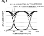
- Fig. 8 is a graph illustrating the signal amount obtained at each position of the photodiode array.
- the horizontal axis represents the scanning position ( ⁇ m) along a predetermined scanning direction in the photodiode array
- the vertical axis represents a normalized current i.e. signal amount obtained at each position, the current being normalized taking as 1 the maximum value of the below-described graph G2.
- the graph G1 depicts the current value change along the scanning direction S1 (including the carrier capturing regions 13)
- the graph G2 depicts the current value change along the scanning direction S2 (not including the carrier capturing regions 13), in the constitution example (a) of Fig. 5 .
- the other graphs illustrate current values obtained in each photodiode prior to addition.
- crosstalk capturing and drawing effects between photodiodes are also achieved in graph G2 obtained for the scanning direction S2 where no carrier capturing regions 13 are formed, although somewhat less effectively than in graph G1 for the scanning direction S1 where carrier capturing regions 13 are formed.
- the antiblooming effect by the carrier capturing portion 12 can be reliably achieved by using a constitution wherein, as described above, the distance to the nearest carrier capturing region 13 (p-type region 11) is smaller than the distance to the adjacent photosensitive region 3, at all points on the periphery of the photosensitive region 3 (p-type region 7).
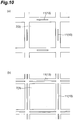
- the high-concentration n-type regions 9 formed between the p-type regions 7 of the photosensitive regions 3 and the p-type regions 11 of the carrier capturing regions 13 can be formed to various patterns in accordance with the constitution of the carrier capturing portion 12, as illustrated for example schematically with dashed lines in the constitution examples (a) and (b) of Fig. 9 .
- the constitution example (a) of Fig. 9 corresponds herein to the constitution illustrated in Fig. 1 .
- Figs. 10 to 12 depict only the constitutions of the photosensitive regions 3 (p-type regions 7) and of the carrier capturing regions 13 (p-type regions 11), omitting the constitutions of the high-concentration n-type regions 9 and so forth.
- a carrier capturing portion 12 comprising four carrier capturing regions 13 surrounding the photosensitive region 3, one at each side, left, right, bottom and top of the photosensitive region 3 of the photodiode.
- the number of carrier capturing regions 13 is the same as in the constitution example (a), but whereas in the constitution example (a) the carrier capturing region 13 is provided for a central portion of the corresponding side of the photosensitive region 3, in the constitution example (b) the carrier capturing region 13 is provided over the entirety of the corresponding side of the photosensitive region 3, with intervals at the corner sections of the photosensitive region 3, where the carrier capturing regions are not provided.
- cross-shaped carrier capturing regions 13 corresponding to the corner sections of the photosensitive region 3 are provided in addition to the carrier capturing regions 13 in the constitution example (a) of Fig. 10 .
- the carrier capturing regions provided at the central portions of each side of the photosensitive region 3 are absent, so that the carrier capturing portion 12 comprises only cross-shaped carrier capturing regions 13 extending from the corner sections of the photosensitive region 3.
- the region pattern of the carrier capturing regions 13 in the carrier capturing portion 12 is a fine dot pattern.
- the carrier capturing regions 13 are alternately arranged in two parallel arranging directions running between adjacent photosensitive regions 3, and in which the arranging positions for the carrier capturing regions 13 are shifted relative to one another.
- the electrodes provided on the detecting surface 5b side of the semiconductor substrate 5 there may be formed a first electrode electrically connected to the carrier capturing regions 13 of the carrier capturing portion 12, and a second electrode electrically connected to the high-concentration n-type regions 9, such that the first electrode and the second electrode are respectively connected to reference potentials while being electrically insulated from each other.
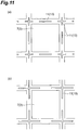
- Figs. 13 and 14 are both plan-view diagrams illustrating schematically the constitution of another embodiment of a semiconductor photodetector according to the present invention.
- Fig. 15 is a side-view cross-sectional diagram illustrating the cross-sectional constitution of the semiconductor photodetector of Figs. 13 and 14 taken along the line II-II.
- the constitution of a photodiode array PD2 will be described as another example of the constitution of a semiconductor photodetector according to the present invention.
- Each electrode 31 includes an electrode conductor 33, a UBM and a bump electrode 35.
- the electrode conductor 33 is made of an aluminum film, for example, and is electrically connected to the high-concentration n-type region 9 through a contact hole formed in a thermally oxidized film. As shown in Figs. 14 and 15 , the electrode conductor 33 is formed so as to cover the high-concentration n-type region 9 as seen from the detecting surface 5b side of the semiconductor substrate 5.
- the UBM is formed, for example, by plating the electrode conductor 33 with Ni and Au in succession.
- the bump electrode 35 is made of solder, and is formed on the UBM.
- the electrode 31 is connected to the non-inverting input terminal of a differential amplifier 27, whereas a middle part of a lead between the electrode 31 and the non-inverting input terminal of the differential amplifier 27 is connected to a reference potential (for example a ground potential). Therefore, the electrode 31 and the non-inverting input terminal of the differential amplifier 27 are connected to a common reference potential.
- Each electrode 41 includes an electrode conductor 43, a UBM, and a bump electrode 45.
- the electrode conductor 43 is made of an aluminum film, for example, and is electrically connected to the p-type region 11 of the carrier capturing region 13 through a contact hole formed in the thermally oxidized film. As shown in Figs. 14 and 15 , the electrode conductor 43 is formed so as to cover the carrier capturing portion 12 where the p-type regions 11 are arranged, as seen from the detecting surface 5b side of the semiconductor substrate 5.
- the UBM is formed, for example, by plating the electrode conductor 43 with Ni and Au in succession.
- the bump electrode 45 is made of solder, and is formed on the UBM.
- the electrodes 41 are electrically insulated from the electrodes 31. While being electrically insulated from the electrodes 31, the electrodes 41 are connected to a reference potential (for example, a ground potential) different from that for the electrodes 31 on the outside of the photodiode array PD2.
- a reference potential for example, a ground potential
- the p-type regions 11 of the carrier capturing regions 13 and the high-concentration n-type regions 9 are electrically separated inside the photodiode array PD2. This prevents the potential on the carrier capturing region 13 side from fluctuating, which allows restraining current from flowing in as a result of the potential difference between the photosensitive regions 3 of the photodiodes and the carrier capturing regions 13. As a result, output signals from photodiodes are less likely to be electrically affected, whereby a stable signal output can be realized.
- various other constitutions may be used as the electrode constitutions.
- the semiconductor photodetector and radiation detecting apparatus according to the present invention are not limited to the above-described embodiments and constitution examples, and may be subject to various modifications.
- the present invention is used in photodiode arrays where a plurality of pn junction-type photodiodes are arranged in a two-dimensional array, however, the invention is not limited thereto, and can also be suitably used in photodiode arrays where a plurality of photodiodes are arranged in a one-dimensional array, for example.
- the semiconductor photodetector and radiation detecting apparatus according to the present invention can also be suitably used in X-ray CT apparatuses.
- the semiconductor photodetector comprises (1) a semiconductor substrate, one face of which is an incident surface of light to be detected; (2) a plurality of pn junction-type photodiodes formed on the side of a detecting surface that is the opposite surface to the incident surface of the semiconductor substrate; and (3) a carrier capturing portion formed between adjacent photodiodes among the plurality of photodiodes, on the detecting surface side of the semiconductor substrate; (4) wherein the carrier capturing portion has one or a plurality of carrier capturing regions, respectively including pn-junctions, arranged at intervals.
- the carrier capturing portion is preferably formed in such a way that at least one photodiode among the plurality of photodiodes is surrounded by the plurality of carrier capturing regions arranged at intervals, as seen from the detecting surface side.
- the carriers that would flow into adjacent photodiodes are reliably removed, which allows suppressing crosstalk generation more favorably. Flow of carriers into adjacent photodiodes can be suppressed yet more effectively thereby, even when a certain photodiode falls into an electrically floating state because of a breakage of a connecting point.
- a high-concentration impurity semiconductor region having the same conductivity type as the semiconductor substrate is preferably formed on the detecting surface side of the semiconductor substrate, between the carrier capturing portion and the photodiode.
- the high-concentration impurity semiconductor region has herein a function of separating adjacent photodiodes (channel stopper), for electrically separating adjacent photodiodes. Crosstalk between photodiodes can be further reduced as a result. Flow of carriers into adjacent photodiodes can be suppressed yet more effectively thereby, even when a certain photodiode falls into an electrically floating state because of a breakage of a connecting point.
- the high-concentration impurity semiconductor region is preferably formed so as to surround at least one photodiode among the plurality of photodiodes, as seen from the detecting surface side. Adjacent photodiodes can then be electrically separated reliably.
- an electrode is preferably formed on the detecting surface side of the semiconductor substrate, the electrode being electrically connected to the carrier capturing region of the carrier capturing portion and to the high-concentration impurity semiconductor region, the electrode being connected to a reference potential.
- This allows sharing of the electrodes for connecting the carrier capturing regions to the reference potential, and the electrodes for connecting the high-concentration impurity semiconductor regions to the reference potential, whereby the number of electrodes can be prevented from increasing.
- the carriers drawn from the carrier capturing regions disappear inside the semiconductor photodetector. Crosstalk between photodiodes can be reduced as a result. Flow of carriers into adjacent photodiodes can be reduced thereby, even when a certain photodiode falls into an electrically floating state because of a breakage of a connecting point.
- the electrodes there may be formed a first electrode electrically connected to the carrier capturing region of the carrier capturing portion, and a second electrode electrically connected to the high-concentration impurity semiconductor region on the detecting surface side of the semiconductor substrate, such that the first electrode and the second electrode are respectively connected to reference potentials while being electrically insulated from each other.
- the carrier capturing regions and the high-concentration impurity semiconductor regions are electrically separated inside the semiconductor photodetector. This prevents the potential on the carrier capturing region side from fluctuating, which allows restraining current from flowing in because of the potential difference between the photodiodes and the carrier capturing regions. As a result, output signals from photodiodes are less likely to be electrically affected, whereby a stable signal output can be realized.
- the semiconductor substrate is of a first conductive type
- the plurality of photodiodes and the one or plurality of carrier capturing regions comprise each a second conductive type impurity semiconductor region and the semiconductor substrate.
- the high-concentration impurity semiconductor region is of the first conductive type, as is the semiconductor substrate.
- the region width w of the carrier capturing regions that constitute the carrier capturing portion is preferably no less than 1 ⁇ m.
- the region length L of the carrier capturing regions is preferably no less than 1 ⁇ m.
- the carrier capturing regions are preferably arranged with an interval such that depletion layers do not come into contact between two adjacent carrier capturing regions.
- the carrier capturing regions are preferably formed in such a way that a distance from the corresponding photodiode to the carrier capturing regions is smaller than a distance to the adjacent photodiodes, at all points on the periphery of the photodiode.
- the radiation detecting apparatus there can be used a constitution comprising a semiconductor photodetector having the above-described constitution and a scintillator positioned on the incident surface side of the semiconductor substrate, for emitting light in response to radiation incident thereon.
- a photodetecting element having the above-described constitution allows favorably suppressing the occurrence of crosstalk between photodiodes, as described above. Flow of carriers into adjacent photodiodes can be suppressed thereby, even when a certain photodiode falls into an electrically floating state because of a breakage of a connecting point. A high resolution can be attained as a result.
- the present invention can provide a semiconductor photodetector and a radiation detecting apparatus which can favorably restrain crosstalk from occurring.
Applications Claiming Priority (2)
| Application Number | Priority Date | Filing Date | Title |
|---|---|---|---|
| JP2006344902A JP5085122B2 (ja) | 2006-12-21 | 2006-12-21 | 半導体光検出素子及び放射線検出装置 |
| PCT/JP2007/073747 WO2008075577A1 (en) | 2006-12-21 | 2007-12-04 | Semiconductor photodetector and radiation detecting apparatus |
Publications (2)
| Publication Number | Publication Date |
|---|---|
| EP2092563A1 EP2092563A1 (en) | 2009-08-26 |
| EP2092563B1 true EP2092563B1 (en) | 2018-09-19 |
Family
ID=39099864
Family Applications (1)
| Application Number | Title | Priority Date | Filing Date |
|---|---|---|---|
| EP07850321.6A Not-in-force EP2092563B1 (en) | 2006-12-21 | 2007-12-04 | Semiconductor photodetector and radiation detecting apparatus |
Country Status (6)
| Country | Link |
|---|---|
| US (1) | US8084836B2 (ja) |
| EP (1) | EP2092563B1 (ja) |
| JP (1) | JP5085122B2 (ja) |
| CN (2) | CN101563779B (ja) |
| IL (1) | IL198839A (ja) |
| WO (1) | WO2008075577A1 (ja) |
Families Citing this family (6)
| Publication number | Priority date | Publication date | Assignee | Title |
|---|---|---|---|---|
| JP5150283B2 (ja) | 2008-01-30 | 2013-02-20 | 浜松ホトニクス株式会社 | 固体撮像装置 |
| JP5357488B2 (ja) * | 2008-10-06 | 2013-12-04 | 浜松ホトニクス株式会社 | 放射線検出器及びその製造方法 |
| US20100108893A1 (en) * | 2008-11-04 | 2010-05-06 | Array Optronix, Inc. | Devices and Methods for Ultra Thin Photodiode Arrays on Bonded Supports |
| JP5247488B2 (ja) * | 2009-01-16 | 2013-07-24 | 浜松ホトニクス株式会社 | フォトダイオードアレイ及び放射線検出器 |
| US9466638B2 (en) * | 2014-10-07 | 2016-10-11 | Terapede Systems Inc. | Seemless tiling and high pixel density in a 3D high resolution x-ray sensor with integrated scintillator grid for low noise and high image quality |
| JP7178819B2 (ja) * | 2018-07-18 | 2022-11-28 | 浜松ホトニクス株式会社 | 半導体光検出装置 |
Citations (1)
| Publication number | Priority date | Publication date | Assignee | Title |
|---|---|---|---|---|
| DE4442853A1 (de) * | 1994-12-01 | 1995-10-26 | Siemens Ag | Photodiodenarray |
Family Cites Families (26)
| Publication number | Priority date | Publication date | Assignee | Title |
|---|---|---|---|---|
| JPH0828493B2 (ja) | 1989-11-06 | 1996-03-21 | 富士通株式会社 | 光検知器 |
| JPH0430577A (ja) * | 1990-05-28 | 1992-02-03 | Canon Inc | 固体撮像素子 |
| JPH05167056A (ja) * | 1991-12-17 | 1993-07-02 | Olympus Optical Co Ltd | 積層型固体撮像装置 |
| DE4439995A1 (de) * | 1994-11-09 | 1996-05-15 | Siemens Ag | Photodiodenarray |
| DE19729413C1 (de) | 1997-07-09 | 1998-11-19 | Siemens Ag | Verfahren zum Herstellen eines Flachbildverstärkers und somit hergestellter Flachbildverstärker |
| JP3939430B2 (ja) | 1998-04-03 | 2007-07-04 | 富士通株式会社 | 光検出素子 |
| US6424022B1 (en) * | 2000-03-12 | 2002-07-23 | Mobilink Telecom, Inc. | Guard mesh for noise isolation in highly integrated circuits |
| CN1324714C (zh) | 2000-04-04 | 2007-07-04 | 浜松光子学株式会社 | 半导体能束探测元件 |
| JP2001352094A (ja) | 2000-04-06 | 2001-12-21 | Hamamatsu Photonics Kk | ホトダイオードアレイ |
| US6426991B1 (en) * | 2000-11-16 | 2002-07-30 | Koninklijke Philips Electronics N.V. | Back-illuminated photodiodes for computed tomography detectors |
| JP4707885B2 (ja) | 2001-06-26 | 2011-06-22 | 浜松ホトニクス株式会社 | 光検出素子 |
| JP2003004855A (ja) | 2001-06-26 | 2003-01-08 | Hamamatsu Photonics Kk | 放射線検出器 |
| US6510195B1 (en) * | 2001-07-18 | 2003-01-21 | Koninklijke Philips Electronics, N.V. | Solid state x-radiation detector modules and mosaics thereof, and an imaging method and apparatus employing the same |
| JP4482253B2 (ja) * | 2001-09-12 | 2010-06-16 | 浜松ホトニクス株式会社 | ホトダイオードアレイ、固体撮像装置、及び、放射線検出器 |
| JP2003086827A (ja) | 2001-09-12 | 2003-03-20 | Hamamatsu Photonics Kk | ホトダイオードアレイ、固体撮像装置、及び、放射線検出器 |
| JP3860758B2 (ja) | 2002-02-07 | 2006-12-20 | 浜松ホトニクス株式会社 | 放射線検出器 |
| JP3975091B2 (ja) | 2002-02-12 | 2007-09-12 | 浜松ホトニクス株式会社 | 放射線検出器 |
| JP4012743B2 (ja) | 2002-02-12 | 2007-11-21 | 浜松ホトニクス株式会社 | 光検出装置 |
| JP3974794B2 (ja) | 2002-02-12 | 2007-09-12 | 浜松ホトニクス株式会社 | 放射線検出器 |
| JP2003232860A (ja) | 2002-02-12 | 2003-08-22 | Hamamatsu Photonics Kk | 放射線検出器 |
| KR20030090865A (ko) * | 2002-05-22 | 2003-12-01 | 동부전자 주식회사 | 시모스 이미지 센서 |
| US6747294B1 (en) * | 2002-09-25 | 2004-06-08 | Polarfab Llc | Guard ring structure for reducing crosstalk and latch-up in integrated circuits |
| US7170143B2 (en) | 2003-10-20 | 2007-01-30 | Hamamatsu Photonics K.K. | Semiconductor photo-detection device and radiation apparatus |
| KR100508864B1 (ko) * | 2003-10-23 | 2005-08-17 | 동부아남반도체 주식회사 | 씨모스 이미지 센서 및 이의 제조 방법 |
| JP4525144B2 (ja) * | 2004-04-02 | 2010-08-18 | ソニー株式会社 | 固体撮像素子及びその製造方法 |
| WO2006011274A1 (ja) | 2004-07-30 | 2006-02-02 | Matsushita Electric Industrial Co., Ltd. | 光検出器 |
-
2006
- 2006-12-21 JP JP2006344902A patent/JP5085122B2/ja active Active
- 2006-12-27 US US11/645,800 patent/US8084836B2/en active Active
-
2007
- 2007-12-04 CN CN2007800472706A patent/CN101563779B/zh active Active
- 2007-12-04 CN CN201110414432.3A patent/CN102446945B/zh active Active
- 2007-12-04 EP EP07850321.6A patent/EP2092563B1/en not_active Not-in-force
- 2007-12-04 WO PCT/JP2007/073747 patent/WO2008075577A1/en active Application Filing
-
2009
- 2009-05-20 IL IL198839A patent/IL198839A/en active IP Right Grant
Patent Citations (1)
| Publication number | Priority date | Publication date | Assignee | Title |
|---|---|---|---|---|
| DE4442853A1 (de) * | 1994-12-01 | 1995-10-26 | Siemens Ag | Photodiodenarray |
Also Published As
| Publication number | Publication date |
|---|---|
| CN101563779B (zh) | 2012-02-29 |
| EP2092563A1 (en) | 2009-08-26 |
| US8084836B2 (en) | 2011-12-27 |
| US20080149943A1 (en) | 2008-06-26 |
| JP2008159711A (ja) | 2008-07-10 |
| CN102446945A (zh) | 2012-05-09 |
| IL198839A (en) | 2017-04-30 |
| WO2008075577A1 (en) | 2008-06-26 |
| CN102446945B (zh) | 2015-07-15 |
| CN101563779A (zh) | 2009-10-21 |
| IL198839A0 (en) | 2010-02-17 |
| JP5085122B2 (ja) | 2012-11-28 |
Similar Documents
| Publication | Publication Date | Title |
|---|---|---|
| US10908302B2 (en) | Semiconductor photo-detection device and radiation detection apparatus | |
| US11888003B2 (en) | Photodetector | |
| US5070380A (en) | Transfer gate for photodiode to CCD image sensor | |
| EP2092563B1 (en) | Semiconductor photodetector and radiation detecting apparatus | |
| CN109937485B (zh) | 光检测装置 | |
| CN113167637A (zh) | 光检测装置 | |
| WO2020121851A1 (ja) | 光検出装置 | |
| JP2017208501A (ja) | 光電変換素子 | |
| EP2763189B1 (en) | Radiation detector | |
| US9520516B2 (en) | Photodetection semiconductor device having light receiving element | |
| TW202347505A (zh) | 光檢測器 | |
| JPWO2019180898A1 (ja) | 固体撮像素子 | |
| JPH04254377A (ja) | 受光素子アレイおよびその信号処理回路の実装構造 | |
| JP2006179696A (ja) | 固体撮像装置 |
Legal Events
| Date | Code | Title | Description |
|---|---|---|---|
| PUAI | Public reference made under article 153(3) epc to a published international application that has entered the european phase |
Free format text: ORIGINAL CODE: 0009012 |
|
| 17P | Request for examination filed |
Effective date: 20090428 |
|
| AK | Designated contracting states |
Kind code of ref document: A1 Designated state(s): AT BE BG CH CY CZ DE DK EE ES FI FR GB GR HU IE IS IT LI LT LU LV MC MT NL PL PT RO SE SI SK TR |
|
| DAX | Request for extension of the european patent (deleted) | ||
| 17Q | First examination report despatched |
Effective date: 20111013 |
|
| GRAP | Despatch of communication of intention to grant a patent |
Free format text: ORIGINAL CODE: EPIDOSNIGR1 |
|
| INTG | Intention to grant announced |
Effective date: 20180528 |
|
| GRAS | Grant fee paid |
Free format text: ORIGINAL CODE: EPIDOSNIGR3 |
|
| GRAA | (expected) grant |
Free format text: ORIGINAL CODE: 0009210 |
|
| AK | Designated contracting states |
Kind code of ref document: B1 Designated state(s): AT BE BG CH CY CZ DE DK EE ES FI FR GB GR HU IE IS IT LI LT LU LV MC MT NL PL PT RO SE SI SK TR |
|
| REG | Reference to a national code |
Ref country code: GB Ref legal event code: FG4D |
|
| REG | Reference to a national code |
Ref country code: CH Ref legal event code: EP |
|
| REG | Reference to a national code |
Ref country code: AT Ref legal event code: REF Ref document number: 1044229 Country of ref document: AT Kind code of ref document: T Effective date: 20181015 |
|
| REG | Reference to a national code |
Ref country code: IE Ref legal event code: FG4D |
|
| REG | Reference to a national code |
Ref country code: DE Ref legal event code: R096 Ref document number: 602007056227 Country of ref document: DE |
|
| REG | Reference to a national code |
Ref country code: NL Ref legal event code: MP Effective date: 20180919 |
|
| PG25 | Lapsed in a contracting state [announced via postgrant information from national office to epo] |
Ref country code: SE Free format text: LAPSE BECAUSE OF FAILURE TO SUBMIT A TRANSLATION OF THE DESCRIPTION OR TO PAY THE FEE WITHIN THE PRESCRIBED TIME-LIMIT Effective date: 20180919 Ref country code: FI Free format text: LAPSE BECAUSE OF FAILURE TO SUBMIT A TRANSLATION OF THE DESCRIPTION OR TO PAY THE FEE WITHIN THE PRESCRIBED TIME-LIMIT Effective date: 20180919 Ref country code: BG Free format text: LAPSE BECAUSE OF FAILURE TO SUBMIT A TRANSLATION OF THE DESCRIPTION OR TO PAY THE FEE WITHIN THE PRESCRIBED TIME-LIMIT Effective date: 20181219 Ref country code: GR Free format text: LAPSE BECAUSE OF FAILURE TO SUBMIT A TRANSLATION OF THE DESCRIPTION OR TO PAY THE FEE WITHIN THE PRESCRIBED TIME-LIMIT Effective date: 20181220 Ref country code: LT Free format text: LAPSE BECAUSE OF FAILURE TO SUBMIT A TRANSLATION OF THE DESCRIPTION OR TO PAY THE FEE WITHIN THE PRESCRIBED TIME-LIMIT Effective date: 20180919 |
|
| REG | Reference to a national code |
Ref country code: LT Ref legal event code: MG4D |
|
| PG25 | Lapsed in a contracting state [announced via postgrant information from national office to epo] |
Ref country code: LV Free format text: LAPSE BECAUSE OF FAILURE TO SUBMIT A TRANSLATION OF THE DESCRIPTION OR TO PAY THE FEE WITHIN THE PRESCRIBED TIME-LIMIT Effective date: 20180919 |
|
| REG | Reference to a national code |
Ref country code: AT Ref legal event code: MK05 Ref document number: 1044229 Country of ref document: AT Kind code of ref document: T Effective date: 20180919 |
|
| PG25 | Lapsed in a contracting state [announced via postgrant information from national office to epo] |
Ref country code: PL Free format text: LAPSE BECAUSE OF FAILURE TO SUBMIT A TRANSLATION OF THE DESCRIPTION OR TO PAY THE FEE WITHIN THE PRESCRIBED TIME-LIMIT Effective date: 20180919 Ref country code: EE Free format text: LAPSE BECAUSE OF FAILURE TO SUBMIT A TRANSLATION OF THE DESCRIPTION OR TO PAY THE FEE WITHIN THE PRESCRIBED TIME-LIMIT Effective date: 20180919 Ref country code: IS Free format text: LAPSE BECAUSE OF FAILURE TO SUBMIT A TRANSLATION OF THE DESCRIPTION OR TO PAY THE FEE WITHIN THE PRESCRIBED TIME-LIMIT Effective date: 20190119 Ref country code: RO Free format text: LAPSE BECAUSE OF FAILURE TO SUBMIT A TRANSLATION OF THE DESCRIPTION OR TO PAY THE FEE WITHIN THE PRESCRIBED TIME-LIMIT Effective date: 20180919 Ref country code: NL Free format text: LAPSE BECAUSE OF FAILURE TO SUBMIT A TRANSLATION OF THE DESCRIPTION OR TO PAY THE FEE WITHIN THE PRESCRIBED TIME-LIMIT Effective date: 20180919 Ref country code: CZ Free format text: LAPSE BECAUSE OF FAILURE TO SUBMIT A TRANSLATION OF THE DESCRIPTION OR TO PAY THE FEE WITHIN THE PRESCRIBED TIME-LIMIT Effective date: 20180919 Ref country code: ES Free format text: LAPSE BECAUSE OF FAILURE TO SUBMIT A TRANSLATION OF THE DESCRIPTION OR TO PAY THE FEE WITHIN THE PRESCRIBED TIME-LIMIT Effective date: 20180919 Ref country code: IT Free format text: LAPSE BECAUSE OF FAILURE TO SUBMIT A TRANSLATION OF THE DESCRIPTION OR TO PAY THE FEE WITHIN THE PRESCRIBED TIME-LIMIT Effective date: 20180919 Ref country code: AT Free format text: LAPSE BECAUSE OF FAILURE TO SUBMIT A TRANSLATION OF THE DESCRIPTION OR TO PAY THE FEE WITHIN THE PRESCRIBED TIME-LIMIT Effective date: 20180919 |
|
| PG25 | Lapsed in a contracting state [announced via postgrant information from national office to epo] |
Ref country code: SK Free format text: LAPSE BECAUSE OF FAILURE TO SUBMIT A TRANSLATION OF THE DESCRIPTION OR TO PAY THE FEE WITHIN THE PRESCRIBED TIME-LIMIT Effective date: 20180919 Ref country code: PT Free format text: LAPSE BECAUSE OF FAILURE TO SUBMIT A TRANSLATION OF THE DESCRIPTION OR TO PAY THE FEE WITHIN THE PRESCRIBED TIME-LIMIT Effective date: 20190119 |
|
| REG | Reference to a national code |
Ref country code: DE Ref legal event code: R097 Ref document number: 602007056227 Country of ref document: DE |
|
| PLBE | No opposition filed within time limit |
Free format text: ORIGINAL CODE: 0009261 |
|
| STAA | Information on the status of an ep patent application or granted ep patent |
Free format text: STATUS: NO OPPOSITION FILED WITHIN TIME LIMIT |
|
| PG25 | Lapsed in a contracting state [announced via postgrant information from national office to epo] |
Ref country code: DK Free format text: LAPSE BECAUSE OF FAILURE TO SUBMIT A TRANSLATION OF THE DESCRIPTION OR TO PAY THE FEE WITHIN THE PRESCRIBED TIME-LIMIT Effective date: 20180919 |
|
| REG | Reference to a national code |
Ref country code: CH Ref legal event code: PL |
|
| 26N | No opposition filed |
Effective date: 20190620 |
|
| GBPC | Gb: european patent ceased through non-payment of renewal fee |
Effective date: 20181219 |
|
| PG25 | Lapsed in a contracting state [announced via postgrant information from national office to epo] |
Ref country code: MC Free format text: LAPSE BECAUSE OF FAILURE TO SUBMIT A TRANSLATION OF THE DESCRIPTION OR TO PAY THE FEE WITHIN THE PRESCRIBED TIME-LIMIT Effective date: 20180919 Ref country code: LU Free format text: LAPSE BECAUSE OF NON-PAYMENT OF DUE FEES Effective date: 20181204 |
|
| REG | Reference to a national code |
Ref country code: IE Ref legal event code: MM4A |
|
| REG | Reference to a national code |
Ref country code: BE Ref legal event code: MM Effective date: 20181231 |
|
| PG25 | Lapsed in a contracting state [announced via postgrant information from national office to epo] |
Ref country code: IE Free format text: LAPSE BECAUSE OF NON-PAYMENT OF DUE FEES Effective date: 20181204 Ref country code: FR Free format text: LAPSE BECAUSE OF NON-PAYMENT OF DUE FEES Effective date: 20181231 Ref country code: SI Free format text: LAPSE BECAUSE OF FAILURE TO SUBMIT A TRANSLATION OF THE DESCRIPTION OR TO PAY THE FEE WITHIN THE PRESCRIBED TIME-LIMIT Effective date: 20180919 |
|
| PG25 | Lapsed in a contracting state [announced via postgrant information from national office to epo] |
Ref country code: BE Free format text: LAPSE BECAUSE OF NON-PAYMENT OF DUE FEES Effective date: 20181231 |
|
| PG25 | Lapsed in a contracting state [announced via postgrant information from national office to epo] |
Ref country code: CH Free format text: LAPSE BECAUSE OF NON-PAYMENT OF DUE FEES Effective date: 20181231 Ref country code: GB Free format text: LAPSE BECAUSE OF NON-PAYMENT OF DUE FEES Effective date: 20181219 Ref country code: LI Free format text: LAPSE BECAUSE OF NON-PAYMENT OF DUE FEES Effective date: 20181231 |
|
| PG25 | Lapsed in a contracting state [announced via postgrant information from national office to epo] |
Ref country code: MT Free format text: LAPSE BECAUSE OF NON-PAYMENT OF DUE FEES Effective date: 20181204 |
|
| PGFP | Annual fee paid to national office [announced via postgrant information from national office to epo] |
Ref country code: DE Payment date: 20191119 Year of fee payment: 13 |
|
| PG25 | Lapsed in a contracting state [announced via postgrant information from national office to epo] |
Ref country code: TR Free format text: LAPSE BECAUSE OF FAILURE TO SUBMIT A TRANSLATION OF THE DESCRIPTION OR TO PAY THE FEE WITHIN THE PRESCRIBED TIME-LIMIT Effective date: 20180919 |
|
| PG25 | Lapsed in a contracting state [announced via postgrant information from national office to epo] |
Ref country code: CY Free format text: LAPSE BECAUSE OF FAILURE TO SUBMIT A TRANSLATION OF THE DESCRIPTION OR TO PAY THE FEE WITHIN THE PRESCRIBED TIME-LIMIT Effective date: 20180919 Ref country code: HU Free format text: LAPSE BECAUSE OF FAILURE TO SUBMIT A TRANSLATION OF THE DESCRIPTION OR TO PAY THE FEE WITHIN THE PRESCRIBED TIME-LIMIT; INVALID AB INITIO Effective date: 20071204 |
|
| REG | Reference to a national code |
Ref country code: DE Ref legal event code: R119 Ref document number: 602007056227 Country of ref document: DE |
|
| PG25 | Lapsed in a contracting state [announced via postgrant information from national office to epo] |
Ref country code: DE Free format text: LAPSE BECAUSE OF NON-PAYMENT OF DUE FEES Effective date: 20210701 |