EP2056450B1 - Verstärkerschaltung und anzeigevorrichtung damit - Google Patents
Verstärkerschaltung und anzeigevorrichtung damit Download PDFInfo
- Publication number
- EP2056450B1 EP2056450B1 EP07739729A EP07739729A EP2056450B1 EP 2056450 B1 EP2056450 B1 EP 2056450B1 EP 07739729 A EP07739729 A EP 07739729A EP 07739729 A EP07739729 A EP 07739729A EP 2056450 B1 EP2056450 B1 EP 2056450B1
- Authority
- EP
- European Patent Office
- Prior art keywords
- stage
- circuit
- amplifier
- logical negation
- input
- Prior art date
- Legal status (The legal status is an assumption and is not a legal conclusion. Google has not performed a legal analysis and makes no representation as to the accuracy of the status listed.)
- Not-in-force
Links
- 238000000926 separation method Methods 0.000 claims description 40
- 239000003990 capacitor Substances 0.000 description 52
- 230000003321 amplification Effects 0.000 description 27
- 238000003199 nucleic acid amplification method Methods 0.000 description 27
- 239000004973 liquid crystal related substance Substances 0.000 description 23
- 238000010586 diagram Methods 0.000 description 20
- 230000007423 decrease Effects 0.000 description 5
- 230000001965 increasing effect Effects 0.000 description 5
- 230000000694 effects Effects 0.000 description 4
- 238000000034 method Methods 0.000 description 4
- 230000003247 decreasing effect Effects 0.000 description 3
- 230000010355 oscillation Effects 0.000 description 2
- 238000009877 rendering Methods 0.000 description 2
- 238000005070 sampling Methods 0.000 description 2
- 239000004020 conductor Substances 0.000 description 1
- 238000005401 electroluminescence Methods 0.000 description 1
- 230000002708 enhancing effect Effects 0.000 description 1
- 238000004519 manufacturing process Methods 0.000 description 1
Images


Classifications
-
- G—PHYSICS
- G09—EDUCATION; CRYPTOGRAPHY; DISPLAY; ADVERTISING; SEALS
- G09G—ARRANGEMENTS OR CIRCUITS FOR CONTROL OF INDICATING DEVICES USING STATIC MEANS TO PRESENT VARIABLE INFORMATION
- G09G3/00—Control arrangements or circuits, of interest only in connection with visual indicators other than cathode-ray tubes
- G09G3/20—Control arrangements or circuits, of interest only in connection with visual indicators other than cathode-ray tubes for presentation of an assembly of a number of characters, e.g. a page, by composing the assembly by combination of individual elements arranged in a matrix no fixed position being assigned to or needed to be assigned to the individual characters or partial characters
- G09G3/34—Control arrangements or circuits, of interest only in connection with visual indicators other than cathode-ray tubes for presentation of an assembly of a number of characters, e.g. a page, by composing the assembly by combination of individual elements arranged in a matrix no fixed position being assigned to or needed to be assigned to the individual characters or partial characters by control of light from an independent source
- G09G3/36—Control arrangements or circuits, of interest only in connection with visual indicators other than cathode-ray tubes for presentation of an assembly of a number of characters, e.g. a page, by composing the assembly by combination of individual elements arranged in a matrix no fixed position being assigned to or needed to be assigned to the individual characters or partial characters by control of light from an independent source using liquid crystals
- G09G3/3611—Control of matrices with row and column drivers
- G09G3/3685—Details of drivers for data electrodes
-
- G—PHYSICS
- G09—EDUCATION; CRYPTOGRAPHY; DISPLAY; ADVERTISING; SEALS
- G09G—ARRANGEMENTS OR CIRCUITS FOR CONTROL OF INDICATING DEVICES USING STATIC MEANS TO PRESENT VARIABLE INFORMATION
- G09G2310/00—Command of the display device
- G09G2310/02—Addressing, scanning or driving the display screen or processing steps related thereto
- G09G2310/0264—Details of driving circuits
- G09G2310/027—Details of drivers for data electrodes, the drivers handling digital grey scale data, e.g. use of D/A converters
-
- G—PHYSICS
- G09—EDUCATION; CRYPTOGRAPHY; DISPLAY; ADVERTISING; SEALS
- G09G—ARRANGEMENTS OR CIRCUITS FOR CONTROL OF INDICATING DEVICES USING STATIC MEANS TO PRESENT VARIABLE INFORMATION
- G09G2310/00—Command of the display device
- G09G2310/02—Addressing, scanning or driving the display screen or processing steps related thereto
- G09G2310/0264—Details of driving circuits
- G09G2310/0297—Special arrangements with multiplexing or demultiplexing of display data in the drivers for data electrodes, in a pre-processing circuitry delivering display data to said drivers or in the matrix panel, e.g. multiplexing plural data signals to one D/A converter or demultiplexing the D/A converter output to multiple columns
Definitions
- the present invention relates to amplifier circuits for amplifying analog input signals and driving signal lines based on the amplified signals, and also to a display device using the amplifier circuits to drive data signal lines.
- liquid crystal display devices When driving a data signal line (also referred to as a "source line”), liquid crystal display devices use a method in which a D/A converter is used to convert a digital video signal into an analog video signal, and an amplifier circuit (also referred to as an “amplifier” , an “output circuit” , or an “analog buffer”) provided at the subsequent stage of the D/A converter is used to amplify the analogvideo signal, which amplified signal is used to drive the data signal line.
- an amplifier circuit also referred to as an "amplifier” , an “output circuit” , or an “analog buffer”
- the reason for using this method is that the data signal line has a large capacitive component, and therefore voltage on the data signal line cannot be changed at a sufficient rate by simply driving the data signal line based on an output signal from the D/A converter.
- Patent Document 1 describes an amplifier circuit configured by cascading three inverters, in which a resistive element and a capacitive element are provided in the second-stage inverter.
- Patent Document 2 describes an amplifier circuit including an input amplification stage and an output amplification stage, in which a resistive circuit is interposed between an output terminal of the output amplification stage and a signal output terminal.
- the amplifier circuit described in Patent Document 1 has problems such as increased circuit complexity due to the resistive element and the capacitive element provided in the second-stage inverter, and high power consumption by the last-stage inverter.
- the amplifier circuit described in Patent Document 2 has a problem where the rate of change (hereinafter, referred to as the "slew rate") of the voltage on the signal line decreases due to the resistive circuit provided for the output terminal of the output amplification stage.
- the present invention aims to provide an amplifier circuit having enhanced stability and low-power-consumption capability with the slew rate maintained, and also to provide a display device including the same.
- a first aspect of the present invention is directed to an amplifier circuit for amplifying an analog input signal and driving a signal line based on the amplified signal, the circuit including:
- the first transistor has a lower channel width-to-length ratio than the second transistor.
- the amplifying portion includes:
- the amplifying portion further includes an input capacitive element having an electrode connected to the input terminal of the first-stage logical negation circuit, and another electrode supplied with a constant voltage , and the input capacitive element has a capacitance value not allowing the threshold setting switch associated with the first-stage logical negation circuit to be rendered conductive when the feedback control switch is rendered conductive, provided that the analog input signal is at a level within a predetermined range.
- the first-stage logical negation circuit included in the amplifying portion has a logic threshold voltage not allowing the threshold setting switch associated with the first-stage logical negation circuit to be rendered conductive when the feedback control switch is rendered conductive, provided that the analog input signal is at a level within a predetermined range.
- the amplifying portion includes:
- the second-from-last-stage logical negation circuit included in the amplifying portion includes a third transistor of the first conduction type having a source terminal supplied with the first source voltage and a gate terminal supplied with an output signal from the previous-stage amplifier, and a fourth transistor of the second conduction type having a source terminal supplied with the second source voltage and a gate terminal supplied with the same output signal from the previous-stage amplifier, and the third transistor has a lower current drive capability than the fourth transistor.
- the separation switch is made up of a single transistor having a conductive terminal connected to a drain terminal of the first transistor and another conductive terminal connected to a drain terminal of the second transistor.
- the separation switch is made up of a single transistor having a conductive terminal supplied with the second source voltage and another conductive terminal connected to a drain terminal of the second transistor.
- the amplifying portion further includes an input capacitive element having an electrode connected to the input terminal of the first-stage logical negation circuit and another electrode supplied with a constant voltage, and the input capacitive element has a capacitance value not allowing the threshold setting switch associated with the first-stage logical negation circuit to be rendered conductive when the feedback control switch is rendered conductive , provided that the analog input signal is at a level within a predetermined range.
- the first-stage logical negation circuit included in the amplifying portion has a logic threshold voltage not allowing the threshold setting switch associated with the first-stage logical negation circuit to be rendered conductive when the feedback control switch is rendered conductive, provided that the analog input signal is at a level within a predetermined range.
- the amplifying portion includes:
- the amplifying portion further includes:
- the amplifying portion further includes:
- a fifteenth aspect of the present invention is directed to a matrix-type display device including:
- the voltage on the signal line varies for a while after the separation switch is rendered conductive, due to current flowing through the second transistor included in the last-stage amplifier. Accordingly, the rate of change of the voltage on the signal line does not change by reducing the current drive capability of the first transistor.
- the output resistance of the last-stage amplifier increases, so that the amplifier circuit has frequency characteristics with an increased phase margin, resulting in reduced power consumption of the amplifier circuit. As such, it is possible to enhance stability and low-power-consumption capability of the amplifier circuit, while maintaining the slew rate.
- the last-stage amplifier including the second transistor, and the first transistor having a lower current drive capability than the second transistor.
- the amplifying portion using n (where n is an odd number) logical negation circuits , n threshold setting switches, n capacitive elements (first-stage and interstage capacitive elements), and a feedback control switch, making it possible to enhance stability and low-power-consumption capability of an amplifier circuit configured by cascading the n logical negation circuits, while maintaining the slew rate.
- the threshold setting switch associated with the first-stage logical negation circuit is prevented from being rendered conductive, making it possible to prevent any amplification error.
- n where n is an odd number
- logical negation circuits (n-1) threshold setting switches, (n-1) capacitive elements (first-stage and interstage capacitive elements), and a feedback control switch, making it possible to enhance stability and low-power-consumption capability of an amplifier circuit configured by cascading the n logical negation circuits, while maintaining the slew rate.
- no threshold setting switch and interstage capacitive element are provided in association with the last-stage logical negation circuit, and therefore it is possible to reduce circuit complexity by a corresponding degree.
- the amplification factor of the last-stage logical negation circuit can be prevented from decreasing excessively.
- the circuit complexity of the amplifier circuit can be reduced.
- the threshold setting switch associated with the first-stage logical negation circuit is prevented from being rendered conductive, making it possible to prevent any amplification error.
- the amplifying portion using a logical negation circuit and a differential amplifier, making it possible to enhance stability and low-power-consumption capability of an amplifier circuit configured by cascading the differential amplifier and the logical negation circuit, while maintaining the slew rate.
- the amplifier control switch and the input control switch it is possible to suitably control the amplifier control switch and the input control switch to invert and amplify the difference between the analog input signal and the output signal from the logical negation circuit in the differential amplifier.
- the data signal lines are driven using the amplifier circuit having enhanced stability and low-power-consumption capability with the slew rate maintained, and therefore it is possible to enhance image quality and low-power-consumption capability of a display device, while maintaining display speed.
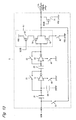
- FIG. 1 is a circuit diagram for an amplifier circuit according to a first embodiment of the present invention.
- the amplifier circuit 1 shown in FIG. 1 uses a plurality of cascaded amplifiers (inverters) to amplify an analog input signal AIN and drive a signal line SL based on the amplified signal (details will be described later).
- the amplifier circuit 1 is used, for example, when driving a data signal line in a liquid crystal display device.
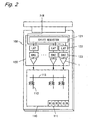
- FIG. 2 is a block diagram illustrating the configuration of a liquid crystal display device including the amplifier circuits 1.
- the liquid crystal display device shown in FIG. 2 has a pixel array 110, a data signal line drive circuit 120, and a scanning signal line drive circuit (not shown) integrally formed on a liquid crystal panel 100.
- the pixel array 110 includes a plurality of two-dimensionally arranged pixel circuits 111, a plurality of data signal lines 112, and a plurality of scanning signal lines 113.
- the data signal lines 112 are each connected commonly to the pixel circuits 111 arranged in the same column, whereas the scanning signal lines 113 are each connected commonly to the pixel circuits 111 arranged in the same row.
- the scanning signal line drive circuit sequentially selects and activates the scanning signal lines 113, thereby sequentially selecting the pixel circuits 111 for one row.
- the data signal line drive circuit 120 drives the data signal lines 112 in a line-sequential manner based on digital video signals DIN.
- the pixel array 110 includes m (where m is an integer of 2 or more) data signal lines 112, and the digital video signal DIN is a k-bit signal. Also, an interval in which the digital video signal DIN changes is referred to as a "cycle".
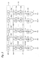
- FIG. 3 is a block diagram illustrating a detailed configuration of the data signal line drive circuit 120.
- the data signal line drive circuit 120 includes an m -stage shift register 121, 2 m latches 122 (which are grouped into m input-side latches 122a and m output-side latches 122b), m D/A converters 123, and m amplifier circuits 1, as shown in FIG. 3 .
- the shift register 121 consists of m cascaded flip-flops. In association with each stage of the shift register 121, the k-bit input-side latch 122a, the k-bit output-side latch 122b, the D/A converter 123, and the amplifier circuit 1 are provided.
- a circuit provided in association with the i 'th stage (where i is an integer from 1 to m ) of the shift register is referred to as the " i 'th circuit".
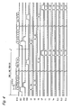
- FIG. 4 is a timing chart for the data signal line drive circuit 120.
- the data signal line drive circuit 120 is supplied with the digital video signal DIN, which changes per cycle.
- a source start pulse SSP (omitted in FIG. 4 ) is brought into a predetermined level (which is assumed hereinafter to be "high level") for one cycle within one line period.
- the shift register 121 shifts the source startpulse SSP by one stage per cycle. Accordingly, output signals SS1 to SS m from the shift register 121 are brought into high level for one cycle in the order: SS1, SS2, ..., SS m .
- the i 'th input-side latch 122a memorizes the digital video signal DIN when the output signal SS i from the shift register 121 changes from high to low level.
- a latch pulse LP is brought into a predetermined level (which is assumed hereinafter to be "high level") for one cycle.
- the latch pulse LP changes from low to high level
- the i 'th output-side latch 122b memorizes the digital video signal memorized in the i 'th input-side latch 122a. This allows the m digital video signals memorized in m input-side latches 122a to be collectively transferred to m output-side latches 122b.
- the i 'th D/A converter 123 converts the digital video signal memorized in the i 'th output-side latch 122b into an analog video signal.
- the i 'th amplifier circuit 1 has an output terminal connected to a data signal line SLi.
- the i 'th amplifier circuit 1 amplifies an analog input signal outputted from the i 'th D/A converter 123 and drives the data signal line SLi based on the amplified signal.
- the amplifier circuit 1 includes inverters 11 to 13 serving as logical negation circuits , switches 21 to 23, capacitors 31 to 33, stop control switches 41 to 43, a feedback control switch 51, a separation switch 61, and an initial setting switch 71, as shown in FIG. 1 .
- the switches 21 to 23, the feedback control switch 51, and the separation switch 61 are analog switches in which a P-type transistor and an N-type transistor are connected in parallel.
- the inverters 11 to 13 are cascaded, and serve as amplifiers independently of each other, as will be described later.
- the inverter 13 includes a P-type transistor 14 and an N-type transistor 15.
- the P-type transistor 14 has a source terminal supplied with a high level source voltage VDD
- the N-type transistor 15 has a source terminal supplied with a low level source voltage VSS via the stop control switch 43.
- Gate terminals of the P-type transistor 14 and the N-type transistor 15 are both connected to an output terminal of the inverter 12 via the capacitor 33. This allows the gate terminals of the P-type transistor 14 and the N-type transistor 15 to be supplied with an output signal from the inverter 12.
- drain terminals of the P-type transistor 14 and the N-type transistor 15 are connected to a common node, which serves as an output terminal of the inverter 13.
- the inverters 11 and 12 are configured similarly.
- the switches 21 to 23 are provided between the input and output terminals of the inverters 11 to 13, respectively, and serve as threshold setting switches for selecting whether or not to short-circuit the input and output terminals of the inverters 11 to 13.
- the capacitor 31 has an electrode connected to an input terminal for the analog input signal AIN, and another electrode connected to the input terminal of the inverter 11.
- the capacitor 31 serves as a first-stage capacitive element provided between the input terminal for the analog input signal AIN and the input terminal of the first-stage inverter 11.
- the capacitor 32 has an electrode connected to the output terminal of the inverter 11, and another electrode connected to the input terminal of the inverter 12.
- the capacitor 33 has an electrode connected to the output terminal of the inverter 12, and another electrode connected to the input terminal of the inverter 13.
- Each of the capacitors 32 and 33 serves as an interstage capacitive element provided between the input terminal of the inverter 12, 13 not provided at the first stage and the output terminal of the inverter 11, 12 provided at the previous stage.
- the stop control switches 41 to 43 are provided between the source terminals of the N-type transistors included in their respective inverters 11 to 13 and the low level source voltage VSS.
- the stop control switches 41 to 43 are controlled based on a common control signal to be turned “ON” when the amplifier circuit 1 is in operation, and "OFF” when in rest.
- the feedback control switch 51 is provided between the output terminal of the inverter 13 and one electrode of the capacitor 31 (the electrode being connected to the input terminal for the analog input signal AIN, which is referred to hereinafter as the "input-side electrode"), and selects whether or not to feed back an output signal from the last-stage inverter 13 to an input to the first-stage inverter 11.
- the inverters 11 to 13, the switches 21 to 23, the capacitors 31 to 33, and the feedback control switch 51 constitute an amplifying portion including a plurality of cascaded amplifiers (the inverters 11 to 13), which negatively feeds back the output signal from the last-stage amplifier (the inverter 13) to the input to the first-stage amplifier (the inverter 11).
- the separation switch 61 is providedbetween the output terminal of the inverter 13 and the signal line SL, and selects whether or not to supply an output signal from the amplifying portion (an output signal from the last-stage inverter 13) to the signal line SL.
- the initial setting switch 71 is provided between the signal line SL and the low level source voltage VSS, and selects whether or not to supply the low level source voltage VSS to the signal line SL.
- the switches 21 to 23 are controlled based on a common control signal (hereinafter, referred to as a "switch control signal SC1").
- the feedback control switch 51 and the separation switch 61 are controlled based on a common control signal (hereinafter, referred to as a “switch control signal SC2”) different from the switch control signal SC1.
- the initial setting switch 71 is controlled based on a negation of the switch control signal SC2 (hereinafter, referred to by "SC2B"). These switches are brought into “ON” state when signals supplied to their control terminals are at high level.
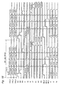
- FIG. 5 is a timing chart for control signals supplied to the amplifier circuit 1.
- the operation of the amplifier circuit 1 will be described below on the assumption that the stop control switches 41 to 43 are in "ON" state.
- the amplifier circuit 1 drives the signal line SL once per line period. Therefore, the switch control signals SC1 and SC2 are each brought into high level once within one line period, as shown in FIG. 5 . More specifically, within one line period, first, the switch control signal SC1 is brought into high level for a predetermined time period t1, and the switch control signal SC1 changes to low level before the switch control signal SC2 is brought into high level for a predetermined time period t2. Note that in FIG. 5 , the switch control signal SC1 changes to high level before the switch control signal SC2 changes to low level, but it may change to high level after the switch control signal SC2 changes to low level.
- each of the initial setting period and the writing period occurs once within one line period.
- the switches 21 to 23 and the initial setting switch 71 are brought into "ON” state, whereas the feedback control switch 51 and the separation switch 61 are brought into “OFF” state. Therefore, during the initial setting period, the signal line SL is connected to the low level source voltage VSS via the initial setting switch 71, so that the voltage on the signal line SL becomes equal to the low level source voltage VSS. In addition, the input and output terminals of the inverters 11 to 13 are short-circuited.
- both the input and output voltages of the inverters 11 to 13 become the logic threshold voltages of the inverters.
- the logic threshold voltages of the inverters match one another, but in fact, there are production variations, and therefore the logic threshold voltages of the inverters do not completely match one another. Accordingly, the capacitor 32 holds the difference in the logic threshold voltage between the inverters 11 and 12, and the capacitor 33 holds the difference in the logic threshold voltage between the inverters 12 and 13.
- the input-side electrode of the capacitor 31 is supplied with the analog input signal AIN, and therefore the capacitor 31 holds the difference between the voltage of the analog input signal AIN (hereinafter, referred to as the "input voltage Va") and the logic threshold voltage of the inverter 11.
- the voltage of the signal line SL becomes equal to the low level source voltage VSS, whereas the input voltages of the inverters 11 to 13 become equal to their respective logic threshold voltages. Thereafter, the writing period starts.
- the switches 21 to 23 and the initial setting switch 71 are brought into "OFF” state, whereas the feedback control switch 51 and the separation switch 61 are brought into “ON” state. Therefore, during the writing period, the signal line SL is connected to the output terminal of the inverter 13 via the separation switch 61, whereas the output terminal of the inverter 13 is connected to the input-side electrode of the capacitor 31 via the feedback control switch 51.
- the input-side electrode of the capacitor 31 is supplied with the output voltage of the inverter 13. Therefore, when the output voltage of the inverter 13 is lower than the input voltage Va, the input-side electrode of the capacitor 31 becomes lower in voltage. Since the capacitors 31 to 33 retain predetermined potential differences, and the inverters 11 to 13 have the characteristics as shown in FIG. 6 , as the input-side electrode of the capacitor 31 becomes lower in voltage, the input voltage of the inverter 11 falls; the output voltage of the inverter 11 and the input voltage of the inverter 12 rise; the output voltage of the inverter 12 and the input voltage of the inverter 13 fall; and the output voltage of the inverter 13 rises.
- the output voltage of the inverter 13 when the output voltage of the inverter 13 is higher than the input voltage Va, the input-side electrode of the capacitor 31 becomes higher in voltage.
- the input voltage of the inverter 11 rises
- the output voltage of the inverter 11 and the input voltage of the inverter 12 fall
- the output voltage of the inverter 12 and the input voltage of the inverter 13 rise
- the output voltage of the inverter 13 falls.
- the output voltage of the inverter 13 rises when it is lower than the input voltage Va, and falls when higher than the input voltage Va, with the result that it ultimately becomes equal to the input voltage Va.
- the inverter serves as an amplifier.
- the input voltages of the inverters 11 to 13 are set at the logic threshold voltage in the initial setting period. Therefore, during the writing period, the inverters 11 to 13 all serve as amplifiers, and when the input voltage of the inverter 11 changes, the output voltage of the inverter 13 changes significantly. Thus, by cascading the inverters 11 to 13 serving as amplifiers, it becomes possible to amplify the analog input signal AIN with a high amplification factor.
- the last-stage inverter 13 included in the amplifier circuit 1 has the following features. While typical inverters consist of P- and N-type transistors having the same current drive capability, the last-stage inverter 13 consists of the P-type transistor 14 and the N-type transistor 15 having different current drive capabilities. More specifically, corresponding to the fact that the initial setting switch 71 is provided between the signal line SL and the low level source voltage VSS, a transistor having a lower current drive capability than the P-type transistor 14 is used as the N-type transistor 15 having a source terminal supplied with the low level source voltage VSS. To this end, a transistor sized smaller than the P-type transistor 14 may be used as the N-type transistor 15. Concretely, the ratio of channel width Wn to channel length Ln (Wn / Ln) of the N-type transistor 15 may be set smaller than the ratio of channel width Wp to channel length Lp (Wp / Lp) of the P-type transistor 14.
- the separation switch 61 and the initial setting switch 71 are alternately brought into "ON" state, so that the voltage on the signal line SL becomes equal to the low level source voltage VSS during the initial setting period, and with the input voltage Va during the writing period.
- the output voltage of the inverter 13 is lower than the input voltage Va, and therefore the output voltage of the inverter 13 (i.e. , the voltage on the signal line SL) rises.
- the reason why the voltage on the signal line SL rises is that current flows from the high level source voltage VDD through the P-type transistor 14 to the signal line SL.
- a single inverter can be represented by an equivalent circuit as shown in FIG. 7 .
- A denotes an amplification factor for a DC component of the inverter
- R denotes a resistance of the inverter
- C denotes a capacitance value of the output stage of the inverter.
- an open-loop gain Ao of the amplifying portion including the inverters 11 to 13 can be given by the following equation (1).
- ⁇ is a signal frequency.
- Ao A ⁇ 1 / 1 + j ⁇ R ⁇ 1 ⁇ C ⁇ 1 ⁇ A ⁇ 2 / 1 + j ⁇ R ⁇ 2 ⁇ C ⁇ 2 ⁇ A ⁇ 3 / 1 + j ⁇ R ⁇ 3 ⁇ C ⁇ 3
- the amplifying portion has frequency characteristics as shown in FIG. 8 .
- the amplification factor is represented by a broken line deflected at pole frequencies (in FIG. 8 , pA and pB), and the phase difference changes by 90° centering about the pole frequencies.
- the minimum from among the values 1 / R1C1, 1 / R2C2, and 1 / R3C3 is the first pole frequency pA
- the second minimum value is the second pole frequency pB.
- the phase difference ⁇ at frequency u where the amplification factor is 1 (0 dB) needs to be about 60° or more.
- 1 / R3C3 is the minimum from among the values 1 / R1C1, 1 / R2C2, and 1 / R3C3, and is set as the first pole frequency pA.
- the N-type transistor 15 has a lower current drive capability than the P-type transistor 14. Accordingly, the inverter 13 has a higher resistance R3 than typical inverters. Therefore, in the case of using the inverter 13 for an amplifying portion, the first pole frequency pA is lower than those of typical inverters.
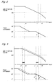
- FIG. 9 is a graph showing frequency characteristics of the amplifier circuit 1.
- the frequency characteristics of the amplifier circuit 1 are indicated by solid lines, and frequency characteristics of an amplifier circuit using typical inverters are indicated by dashed lines.
- the amplifier circuit 1 has a lower first pole frequency (pA' ⁇ pA), and therefore the broken line representing the amplification factor shifts toward a lower frequency.
- the frequency where the amplification factor is 1 decreases from u to u'
- the phase difference at the frequency where the amplification factor is 1 increases from ⁇ to ⁇ '.
- the operational stability of the amplifier circuit 1 is enhanced.
- the resistance as viewed from the output side increases, so that power consumed by the inverter 13 decreases, resulting in decreased power consumption of the entire amplifier circuit 1.
- the voltage on the signal line SL varies for a while after the separation switch 61 is rendered conductive, due to current flowing through the P-type transistor 14 included in the last-stage inverter 13. Accordingly, the rate of change of the voltage on the signal line SL does not change by reducing the current drive capability of the N-type transistor 15.
- the output resistance of the last-stage inverter 13 increases, so that in accordance with the frequency characteristics of the amplifier circuit 1, the phase margin increases, whereas the power consumption of the amplifier circuit 1 decreases. As such, it is possible to enhance the stability and the low-power-consumption capability of the amplifier circuit, while maintaining the slew rate.
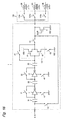
- FIG. 10 is a circuit diagram for an amplifier circuit according to a second embodiment of the present invention.
- the amplifier circuit 2 shown in FIG. 10 is obtained by providing the amplifier circuit 1 according to the first embodiment ( FIG. 1 ) with an inverter 16 (including a separation switch 62) in place of the inverter 13, and omitting the separation switch 61 and the capacitor 33.
- the amplifier circuit 2 can be used for driving a data signal line in a liquid crystal display device (see FIGS. 2 and 3 ).
- the same elements as those in the first embodiment are denoted by the same reference characters, and any descriptions thereof will be omitted.
- the switches 21 and 22 serving as threshold setting switches are respectively provided in associated with the inverters 11 and 12 not provided at the last stage.
- the capacitor 32 serving as an interstage capacitive element is provided between the input terminal of the inverter 12 not provided either at the first or last stage and the output terminal of the inverter 11 at the previous stage.
- the amplifier circuit 2 is used in the case where a substantially desired amplification factor can be achieved with the two inverters 11 and 12.
- the last-stage inverter 16 is not required to have a significantly high amplification factor. Therefore, even when no capacitor is provided between the inverters 12 and 16 so that the logic threshold voltage of the inverter 12 is supplied directly to the input terminal of the inverter 16 during the initial setting period, the inverter 16 is able to amplify an input signal to a required degree.
- the separation switch 62 is made up of a single transistor, and is provided in the inverter 16.
- the separation switch 62 is made up of a single P-type transistor having a source terminal connected to the drain terminal of the P-type transistor 14 included in the inverter 16, and a drain terminal connected to the drain terminal of the N-type transistor 15 included in the inverter 16.
- the separation switch 62 has a gate terminal supplied with a negation (SC2B) of the switch control signal SC2.
- the switch control signal SC2 is brought into low level, and therefore the separation switch 62 is brought into "OFF” state.
- the initial setting switch 71 is in "ON” state, and therefore whether the N-type transistor 15 included in the inverter 16 is in "ON” or “OFF” state, the voltage on the signal line SL becomes equal to the low level source voltage VSS.
- the switch control signal SC2 is brought into high level, and therefore the separation switch 62 is brought into "ON” state. Accordingly, as in the first embodiment, at the beginning of the writing period, current flows from the high level source voltage VDD through the P-type transistor 14 to the signal line SL, thereby increasing the voltage on the signal line SL.
- the separation switch 62 even when the separation switch 62 is used in place of the separation switch 61, it is possible to select whether or not to supply an output signal from the amplifying portion to the signal line SL. In addition, by using the separation switch 62 made up of a single transistor, it becomes possible to reduce the circuit complexity of the amplifier circuit 2.
- the P- and N-type transistors included in the inverter 12 at the second stage from last can be configured in the same manner as used for the last-stage inverter 16, such that the N-type transistor has a lower current drive capability than the P-type transistor.
- the N-type transistor has a lower current drive capability than the P-type transistor.
- An amplifier circuit 3 shown in FIG. 11 is obtained by modifying the amplifier circuit 2 such that the P-type transistor 14 and the separation switch 62 are connected in reverse order within an inverter 17.
- the separation switch 62 is made up of a single P-type transistor having a source terminal supplied with the high level source voltage VDD and a drain terminal connected to the source terminal of the P-type transistor 14.
- the separation switch 62 has a gate terminal supplied with a negation (SC2B) of the switch control signal SC2.
- SC2B negation
- FIG. 12 is a circuit diagram for an amplifier circuit according to a third embodiment of the present invention.
- the amplifier circuit 4 shown in FIG. 12 is obtained by adding a capacitor 34 to the amplifier circuit 2 according to the second embodiment ( FIG. 10 ).
- the amplifier circuit 4 can be used for driving a data signal line in a liquid crystal display device (see FIGS. 2 and 3 ).
- the same elements as those in the first or second embodiment are denoted by the same reference characters, and any descriptions thereof will be omitted.
- the capacitor 34 has an electrode connected to the input terminal of the inverter 11, and another electrode supplied with the low level source voltage VSS.
- the capacitor 34 serves as an input capacitive element having an electrode connected to the input terminal of the first-stage inverter 11, and another electrode supplied with a constant voltage.
- the capacitor 34 has a capacitance value not allowing the switch 21 to be rendered conductive when the feedback control switch 51 is rendered conductive, provided that the input voltage Va is within a predetermined range (between minimum and maximum values).
- the input voltage of the inverter 11 when it is brought into writing state, the input voltage of the inverter 11 might decrease from the logic threshold voltage by up to (the maximum value of the input voltage Va - the low level source voltage VSS). As a result, the switch 21 might be brought into "ON" state, so that charge accumulated in the capacitor 31 might flow through the switch 21, resulting in an amplification error.
- the capacitor 34 having a predetermined capacitance value may be provided at the input terminal of the first-stage inverter 11, as in the amplifier circuit 4.
- Providing the capacitor 34 makes it possible to allow the input voltage of the inverter 11 to only change to such a slight extent as not to render the switch 21 conductive even if the voltage of the input-side electrode of the capacitor 31 changes by the greatest amount.
- the amplifier circuit 4 according to the present embodiment makes it possible to prevent the switch 21 from bringing into "ON" state during the writing state, thereby preventing any amplification error.
- the logic threshold voltage of the first-stage inverter 11 may be increased.
- the inverter 11 may have a logic threshold voltage not allowing the switch 21 to be rendered conductive when the feedback control switch 51 is rendered conductive, provided that the input voltage Va is within a predetermined range. Using such an inverter 11 also makes it possible to prevent any amplification error.
- FIG. 13 a variant similar to that of the second embodiment can be configured for the amplifier circuit 4 according to the present embodiment (see FIG. 13 ).
- An amplifier circuit 5 shown in FIG. 13 operates in a similar manner to the amplifier circuit 4, and achieves similar effects to those achieved by the amplifier circuit 4.
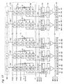
- FIG. 14 is a circuit diagram for an amplifier circuit according to a fourth embodiment of the present invention.
- the amplifier circuit 6 shown in FIG. 14 is obtained by providing the amplifier circuit 1 according to the first embodiment ( FIG. 1 ) with a differential amplifier 18, switches 24, 25, and a capacitor 35, in place of the inverters 11 and 12, the switches 21 and 22, and the capacitors 31 and 32, and omitting the stop control switch 42.
- the amplifier circuit 6 can be used for driving a data signal line in a liquid crystal display device (see FIGS. 2 and 3 ).
- the same elements as those in the first embodiment are denoted by the same reference characters, and any descriptions thereof will be omitted.
- the differential amplifier 18 has a positive-side input terminal connected to the input terminal for the analog input signal AIN.
- the differential amplifier 18 has a negative-side input terminal connected to the input terminal for the analog input signal AIN via the capacitor 35 and the switch 25.
- the differential amplifier 18 has an inverted output terminal connected to one electrode of the capacitor 33.
- the differential amplifier 18 has a non-inverted output terminal connected to the negative-side input terminal of the differential amplifier 18 via the switch 24.
- the stop control switch 41 is provided between a source terminal of an N-type transistor included in the differential amplifier 18 and the low level source voltage VSS.
- the capacitor 35 serves as a first-stage capacitive element having an electrode connected to the negative-side input terminal of the differential amplifier 18.
- the switch 24 serves as an amplifier control switch for selecting whether or not to short-circuit the non-inverted output terminal and the negative-side input terminal of the differential amplifier 18.
- the switch 25 serves as an input control switch for selecting whether or not to provide the analog input signal AIN to an electrode of the capacitor 35 (the electrode being connected to the input terminal for the analog input signal AIN via the switch 25; hereinafter, referred to as the "input-side electrode").
- the differential amplifier 18 inverts and amplifies the difference between the input voltage Va and the output voltage of the inverter 13. A signal outputted from the inverted output terminal of the differential amplifier 18 is supplied to one electrode of the capacitor 33.
- the inverter 13, the differential amplifier 18, the switches 23 to 25, the capacitors 33 and 35, and the feedback control switch 51 constitute an amplifying portion including a plurality of cascaded amplifiers (the differential amplifier 18 and the inverter 13), which negatively feeds back the output signal from the last-stage amplifier (the inverter 13) to an input to the first-stage amplifier (the differential amplifier 18).
- the switches 23 to 25 are controlledbased on the switch control signal SC1.
- the feedback control switch 51 and the separation switch 61 are controlled based on the switch control signal SC2.
- the initial setting switch 71 is controlled based on the negation SC2B of the switch control signal SC2. These switches are brought into "ON" state when the signals supplied to the control terminals are brought into high level.
- the switch control signals SC1 and SC2 change as in the first embodiment (see FIG. 5 ).
- the switches 23 to 25 and the initial setting switch 71 are brought into "ON” state, whereas the feedback control switch 51 and the separation switch 61 are brought into “OFF” state. Therefore, during the initial setting period, the signal line SL is connected to the low level source voltage VSS via the initial setting switch 71, so that the voltage on the signal line SL becomes equal to the low level source voltage VSS.
- the input and output terminals of the inverter 13 are short-circuited via the switch 23, and therefore both the input and output voltages of the inverter 13 become equal to the logic threshold voltage of the inverter 13.
- the non-inverted output terminal and the negative-side input terminal of the differential amplifier 18 are short-circuited via the switch 24 , and therefore the non-inverted output voltage and the negative-side input voltage of the differential amplifier 18 are equalized (hereinafter, which voltage is referred to as an initial voltage Vi; the initial voltage Vi being substantially equal to the input voltage Va).
- the input-side electrode of the capacitor 35 is connected to the input terminal for the analog input signal AIN via the switch 25, and therefore the input voltage Va is applied to the input-side electrode of the capacitor 35.
- the capacitor 33 holds the difference between the logic threshold voltage of the inverter 13 and the inverted output voltage of the differential amplifier 18 with the input voltage Va provided to the positive-side input terminal and the initial voltage Vi provided to the negative-side input terminal, whereas the capacitor 35 holds the difference between the input voltage Va and the initial voltage Vi.
- the feedback control switch 51 and the separation switch 61 are brought into "ON” state, whereas the switches 23 to 25 and the initial setting switch 71 are brought into “OFF” state. Accordingly, during the writing period, the signal line SL is connected to the high level source voltage VDD via the P-type transistor 14 and the separation switch 61 or connected to the low level source voltage VSS via the N-type transistor 15 and the separation switch 61, depending on the output voltage from the differential amplifier 18.
- the negative-side input voltage of the differential amplifier 18 becomes lower than the initial voltage Vi, so that the inverted output voltage of the differential amplifier 18 falls, and the output voltage of the inverter 13 rises.
- the negative-side input voltage of the differential amplifier 18 becomes higher than the initial voltage Vi, so that the inverted output voltage of the differential amplifier 18 rises, and the output voltage of the inverter 13 falls.
- the output voltage of the inverter 13 rises when it is lower than the input voltage Va, and falls when higher than the input voltage Va, with the result that it ultimately becomes equal to the input voltage Va.
- the amplifying portion having the differential amplifier 18 and the inverter 13 cascaded operates in a similar manner to the amplifying portion having three inverters cascaded.
- the amplifier circuit 6 according to the present embodiment makes it possible to enhance the stability and the low-power-consumption capability of the amplifier circuit, while maintaining the slew rate.
- An amplifier circuit 7 shown in FIG. 15 has the switch 24 and the capacitor 35 disposed differently from where they are in the amplifier circuit 6. The difference between the amplifier circuit 7 and the amplifier circuit 6 will be described below.
- the positive-side input terminal of the differential amplifier 18 is connected to the input terminal for the analog input signal AIN via the capacitor 35.
- the negative-side input terminal of the differential amplifier 18 is connected to the input terminal for the analog input signal AIN via the switch 25.
- the inverted output terminal of the differential amplifier 18 is connected to one electrode of the capacitor 33, and also connected to the positive-side input terminal of the differential amplifier 18 via the switch 24.
- the capacitor 35 serves as a first-stage capacitive element having an electrode connected to the positive-side input terminal of the differential amplifier 18, and another electrode provided with the analog input signal AIN.
- the switch 24 serves as an amplifier control switch for selecting whether or not to short-circuit the positive-side input terminal and the inverted output terminal of the differential amplifier 18.
- the switch 25 serves as an input control switch for selecting whether or not to provide the analog input signal AIN to the negative-side input terminal of the differential amplifier 18.
- the inverted output terminal and the positive-side input terminal of the differential amplifier 18 are short-circuited via the switch 24, and therefore the inverted output voltage and the positive-side input voltage of the differential amplifier 18 become equal to the initial voltage Vi substantially equal to the input voltage Va.
- the input voltage Va is applied to the input-side electrode of the capacitor 35 (the electrode being connected to the input terminal for the analog input signal AIN).
- the capacitor 33 holds the difference between the logic threshold voltage of the inverter 13 and the inverted output voltage of the differential amplifier 18 with the initial voltage Vi provided to the positive-side input terminal and the input voltage Va provided to the negative-side input terminal, whereas the capacitor 35 holds the difference between the input voltage Va and the initial voltage Vi.
- the negative-side input voltage of the differential amplifier 18 falls, so that the inverted output voltage of the differential amplifier 18 falls, and the output voltage of the inverter 13 rises.
- the negative-side input voltage of the differential amplifier 18 rises, so that the inverted output voltage of the differential amplifier 18 rises, and the output voltage of the inverter 13 falls. In this manner, the output voltage of the inverter 13 rises when it is lower than the input voltage Va, and falls when higher than the input voltage Va, with the result that it ultimately becomes equal to the input voltage Va.
- the amplifier circuit 7 makes it possible to enhance the stability and the low-power-consumption capability of the amplifier circuit, while maintaining the slew rate.
- a fifth embodiment will be described with respect to other usage patterns of the amplifier circuits according to the embodiments.
- the following description will be given with respect to an example where the amplifier circuit 1 according to the first embodiment is used to drive three data signal lines SR, SG, and SB in a time-division manner.
- selection switches 126r, 126g, and 126b may be provided between the amplifier circuit 1 and the data signal lines SR, SG, and SB, as shown in FIG. 16 , such that one of them can be selectively controlled to be brought into "ON" state.
- FIG. 17 is a block diagram illustrating a detailed configuration of a data signal line drive circuit according to the present embodiment.
- the data signal line drive circuit shown in FIG. 17 three k-bit input-side latches 124a, three k-bit output-side latches 124b, a data selection portion 125, a D/A converter 123, an amplifier circuit 1, and selection switches 126 are provided in association with each stage of a shift register 121.
- FIG. 18 is a timing chart for the data signal line drive circuit according to the present embodiment.
- three digital video signals DIN_R, DIN_G, and DIN_B which change per cycle, are supplied in parallel to the data signal line drive circuit.
- the three input-side latches 124a at the i ' th stage memorize the digital video signals DIN_R, DIN_G, and DIN_B when an output signal SS i from the shift register 121 changes from high to low level.
- a latch pulse LP is brought into high level for one cycle, and the 3 m digital video signals memorized in 3 m input-side latches 124a are collectively transferred to 3 m output-side latches 124b.
- Inputted to the i'th data selection portion 125 are three digital video signals (3k bits in total) outputted from three output-side latches 124b at the i 'th stage, and selection control signals SSD_R, SSD_G, and SSD_B.
- the selection control signals SSD_R, SSD_G, and SSD_B are brought into high level for a predetermined time period once within one line period, and the i 'th data selection portion 125 selects and outputs one (k bits) of the three digital video signals in accordance with the selection control signals SSD_R, SSD_G, and SSD_B. Accordingly, within one line period, the three digital video signals are sequentially selected and outputted from the i 'th data selection portion 125.
- the i 'th D/A converter 123 converts the digital video signal outputted from the i 'th data selection portion 125 into ananalogvideosignal.
- the output terminal of the i 'th amplifier circuit 1 is connected to three data signal lines SR i , SG i , and SBi via the selection switches 126.
- the i 'th amplifier circuit 1 amplifies the analog input signal outputted from the i 'th D/A converter 123, and drives any of the data signal lines SR i , SG i , and SBi based on the amplified signal.
- FIG. 19 is a timing chart for control signals supplied to the amplifier circuit 1 and the selection switches 126.
- the selection switches 126r, 126g, and 126b are brought into "ON" state when their respective sampling control signals SMP_R, SMP_G, and SMP_B are at high level.
- the sampling control signals SMP_R, SMP_G, and SMP_B are brought into high level for a predetermined time period once within one line period.
- the data signal lines SR i , SG i , and SB i are sequentially selected and driven once within one line period.
- the amplifier circuit 1 according to the first embodiment can also be used in a liquid crystal display device in which a plurality of data signal lines are driven in a time-division manner.
- the amplifier circuits 2 to 7 according to the second to fourth embodiments can also be used to configure similar liquid crystal display devices.
- the initial setting switch 71 is provided between the signal line SL and the low level source voltage VSS to select whether or not to supply the low level source voltage VSS to the signal line SL, but alternatively, it may be provided between the signal line SL and the high level source voltage VDD to select whether or not to supply the high level source voltage VDD to the signal line SL.
- a transistor having a lower current drive capability than the N-type transistor 15 is used as the P-type transistor 14 having a source terminal supplied with the high level source voltage VDD.
- the amplifier circuits according to the first to third embodiments include amplifying portions each having three inverters cascaded, but the number of inverters included in the amplifying portion may be arbitrary so long as it is an odd number.
- the third embodiment has been described with respect to the case where the capacitor 34 having a predetermined capacitance value is provided to the amplifier circuit 2 according to the second embodiment (or an inverter having a predetermined logic threshold voltage is used as the first-stage inverter 11), a similar approach may be applied to the amplifier circuit 1 according to the first embodiment.
- the amplifier circuit according to each embodiment of the present invention may be used for driving data signal lines in a liquid crystal display device shown in FIG. 20 .
- a pixel array 110, a shift register 221 and analog switches 222, which constitute a part 220 of a data signal line drive circuit, and a scanning signal line drive circuit (not shown) are integrally formed on a liquid crystal panel 200.
- a D/A converter 230 and an amplifier circuit 240, which constitute the remaining part of the data signal line drive circuit, are provided outside the liquid crystal panel 200. In this manner, the amplifier circuit according to each embodiment of the present invention may be provided outside the liquid crystal panel.
- the amplifier circuit according to each embodiment of the present invention may be used for driving the data signal lines in a dot-sequential manner.
- the amplifier circuit according to each embodiment of the present invention may be used for driving data signal lines of display devices other than the liquid crystal display device (e.g., an organic electroluminescence display device).
- the amplifier circuit of the present invention is characterized by stably operating with low power consumption while maintaining the slew rate, and therefore can be widely used in circuits for amplifying analog input signals to drive signal lines (e.g. , a data signal line drive circuit in a liquid crystal display device).
- drive signal lines e.g. , a data signal line drive circuit in a liquid crystal display device.
Landscapes
- Engineering & Computer Science (AREA)
- Chemical & Material Sciences (AREA)
- Crystallography & Structural Chemistry (AREA)
- Physics & Mathematics (AREA)
- Computer Hardware Design (AREA)
- General Physics & Mathematics (AREA)
- Theoretical Computer Science (AREA)
- Amplifiers (AREA)
- Liquid Crystal Display Device Control (AREA)
- Control Of Indicators Other Than Cathode Ray Tubes (AREA)
Claims (15)
- Verstärkerschaltung zum Verstärken eines analogen Eingangssignals und zum Ansteuern einer Signalleitung (SL) basierend auf dem verstärkten Signal, mit:einem Verstärkungsabschnitt, der mehrere in Kaskade geschaltete Verstärker enthält und ein Ausgangssignal aus dem Verstärker der letzten Stufe zu einem Eingang in den Verstärker der ersten Stufe negativ rückkoppelt;einem Trennschalter (61, 62) zum Auswählen, ob ein Ausgangssignal aus dem Verstärkungsabschnitt der Signalleitung (SL) zuzuführen ist; undeinen Anfangseinstellungsschalter (71) zum Auswählen, ob eine erste Quellenspannung der Signalleitung (SL) zuzuführen ist,wobei der in dem Verstärkungsabschnitt enthaltene Verstärker der letzten Stufe einen ersten Transistor (15) mit einem ersten Leitungstyp, der einen Source-Anschluss, dem die erste Quellenspannung zugeführt wird, und einen Gate-Anschluss, dem ein Ausgangssignal aus dem Verstärker der vorhergehenden Stufe zugeführt wird, besitzt, und einen zweiten Transistor (14) mit einem zweiten Leitungstyp, der einen Source-Anschluss, dem eine zweite Quellenspannung zugeführt wird, und einen Gate-Anschluss, dem dasselbe Ausgangssignal aus dem Verstärker der vorhergehenden Stufe zugeführt wird, besitzt, enthält undwobei der erste Transistor (15) eine geringere Stromansteuerfähigkeit als der zweite Transistor (14) besitzt.
- Verstärkerschaltung nach Anspruch 1, wobei der erste Transistor (15) ein kleineres Kanalbereite-zu-Länge-Verhältnis als der zweite Transistor (14) besitzt.
- Verstärkerschaltung nach Anspruch 1,
wobei der Verstärkungsabschnitt enthält:eine ungeradzahlige Anzahl in Kaskade geschalteter logischer Negationsschaltungen (11, 12, 13, 16, 17), wobei jede als ein Verstärker dient;Schwelleneinstellschalter (21, 22, 23), die in Verbindung mit ihren jeweiligen logischen Negationsschaltungen (11, 12, 13, 16, 17) vorgesehen sind, um auszuwählen, ob die Eingangs- und Ausgangsanschlüsse jeder logischen Negationsschaltung (11, 12, 13, 16, 17) kurzzuschließen sind;einen Rückkopplungssteuerschalter (51) zum Auswählen, ob ein Ausgangssignal aus der logischen Negationsschaltung (13, 16, 17) der letzten Stufe zu einem Eingang in die logische Negationsschaltung der ersten Stufe rückzukoppeln ist;ein kapazitives Element (31) der ersten Stufe, das zwischen einem Eingangsanschluss für das analoge Eingangssignal und dem Eingangsanschluss der logischen Negationsschaltung (11) der ersten Stufe vorgesehen ist; undkapazitive Zwischenstufenelemente (32, 33), die zwischen den Eingangsanschlüssen der logischen Negationsschaltungen (12, 13) außer der logischen Negationsschaltung (11) der ersten Stufe und den Ausgangsanschlüssen der logischen Negationsschaltungen (11, 12) ihrer vorhergehenden Stufe vorgesehen sind. - Verstärkerschaltung nach Anspruch 3,
wobei der Verstärkungsabschnitt ferner ein kapazitives Eingangselement (34) enthält, das eine Elektrode, die mit dem Eingangsanschluss der logischen Negationsschaltung (11) der ersten Stufe verbunden ist, und eine weitere Elektrode, der eine konstante Spannung zugeführt wird, besitzt, und
wobei das kapazitive Eingangselement (34) einen Kapazitätswert besitzt, der nicht erlaubt, dass der der logischen Negationsschaltung (11) der ersten Stufe zugeordnete Schwelleneinstellschalter (21) leitend gemacht wird, wenn der Rückkopplungssteuerschalter (51) leitend gemacht wird, vorausgesetzt, dass sich das analoge Eingangssignal auf einem Pegel innerhalb eines vorgegebenen Bereichs befindet. - Verstärkerschaltung nach Anspruch 3, wobei die logische Negationsschaltung (11) der ersten Stufe, die in dem Verstärkungsabschnitt enthalten ist, eine logische Schwellenspannung besitzt, die nicht erlaubt, dass der der logischen Negationsschaltung (11) der ersten Stufe zugeordnete Schwelleneinstellschalter (21) leitend gemacht wird, wenn der Rückkopplungssteuerschalter (51) leitend gemacht wird, vorausgesetzt, dass sich das analoge Eingangssignal auf einem Pegel innerhalb eines vorgegebenen Bereichs befindet.
- Verstärkerschaltung nach Anspruch 1, wobei der Verstärkungsabschnitt enthält:eine ungeradzahlige Anzahl in Kaskade geschalteter logischer Negationsschaltungen (11, 12, 13, 16, 17), wobei jede als ein Verstärker dient;Schwelleneinstellschalter (21, 22), die in Verbindung mit ihren jeweiligen logischen Negationsschaltungen (11, 12) außer der logischen Negationsschaltung (16, 17) der letzten Stufe vorgesehen sind, um auszuwählen, ob die Eingangs- und Ausgangsanschlüsse jeder logischen Negationsschaltung (11, 12) kurzzuschließen sind;einen Rückkopplungssteuerschalter (51) zum Auswählen, ob ein Ausgangssignal aus der logischen Negationsschaltung (16, 17) der letzten Stufe zu einem Eingang in die logische Negationsschaltung (11) der ersten Stufe rückzukoppeln ist;ein kapazitives Element (31) der ersten Stufe, das zwischen einem Eingangsanschluss für das analoge Eingangssignal und dem Eingangsanschluss der logischen Negationsschaltung (11) der ersten Stufe vorgesehen ist; undein kapazitives Zwischenstufenelement (32), das zwischen dem Eingangsanschluss der logischen Negationsschaltungen (12) außer den logischen Negationsschaltungen (11, 16, 17) der ersten und der letzten Stufe und dem Ausgangsanschluss der logischen Negationsschaltung (11) ihrer vorhergehenden Stufe vorgesehen ist.
- Verstärkerschaltung nach Anspruch 6,
wobei die logische Negationsschaltung (12) der zweitletzten Stufe, die in dem Verstärkungsabschnitt enthalten ist, einen dritten Transistor mit dem ersten Leitungstyp, der einen Source-Anschluss, dem die erste Quellenspannung zugeführt wird, und einen Gate-Anschluss, dem ein Ausgangssignal aus dem Verstärker der vorhergehenden Stufe zugeführt wird, besitzt, und einen vierten Transistor mit dem zweiten Leitungstyp, der einen Source-Anschluss, dem die zweite Quellenspannung zugeführt wird, und einen Gate-Anschluss, dem dasselbe Ausgangssignal aus dem Verstärker der vorhergehenden Stufe zugeführt wird, besitzt, enthält und
wobei der dritte Transistor eine geringere Stromansteuerfähigkeit als der vierte Transistor besitzt. - Verstärkerschaltung nach Anspruch 6, wobei der Trennschalter (62) aus einem einzigen Transistor gebildet ist, der einen leitfähigen Anschluss, der mit einem Drain-Anschluss des ersten Transistors (15) verbunden ist, und einen weiteren leitfähigen Anschluss, der mit einem Drain-Anschluss des zweiten Transistors (14) verbunden ist, besitzt.
- Verstärkerschaltung nach Anspruch 6, wobei der Trennschalter (62) aus einem einzigen Transistor gebildet ist, der einen leitfähigen Anschluss, dem die zweite Quellenspannung zugeführt wird, und einen weiteren leitfähigen Anschluss, der mit einem Drain-Anschluss des zweiten Transistors (14) verbunden ist, besitzt.
- Verstärkerschaltung nach Anspruch 6,
wobei der Verstärkungsabschnitt ferner ein kapazitives Eingangselement (34) enthält, das eine Elektrode, die mit dem Eingangsanschluss der logischen Negationsschaltung (11) der ersten Stufe verbunden ist, und eine weitere Elektrode, der eine konstante Spannung zugeführt wird, besitzt, und
wobei das kapazitive Eingangselement (34) einen Kapazitätswert besitzt, der nicht erlaubt, dass der der logischen Negationsschaltung (11) der ersten Stufe zugeordnete Schwelleneinstellschalter (21) leitend gemacht wird, wenn der Rückkopplungssteuerschalter (51) leitend gemacht wird, vorausgesetzt, dass sich das analoge Eingangssignal auf einem Pegel innerhalb eines vorgegebenen Bereichs befindet. - Verstärkerschaltung nach Anspruch 6, wobei die logische Negationsschaltung (11) der ersten Stufe, die in dem Verstärkungsabschnitt enthalten ist, eine logische Schwellenspannung besitzt, die nicht erlaubt, dass der der logischen Negationsschaltung (11) der ersten Stufe zugeordnete Schwelleneinstellschalter (21) leitend gemacht wird, wenn der Rückkopplungssteuerschalter (51) leitend gemacht wird, vorausgesetzt, dass sich das analoge Eingangssignal auf einem Pegel innerhalb eines vorgegebenen Bereichs befindet.
- Verstärkerschaltung nach Anspruch 1, wobei der Verstärkungsabschnitt enthält:eine logische Negationsschaltung (13), die als der Verstärker der letzten Stufe dient;einen Schwelleneinstellschalter (23) zum Auswählen, ob die Eingangs- und Ausgangsanschlüsse der logischen Negationsschaltung (13) kurzzuschlie-βen sind;einen Differentialverstärker (18), um den Unterschied zwischen dem analogen Eingangssignal und dem Ausgangssignal aus der logischen Negationsschaltung (13) zu invertieren und zu verstärken;einen Rückkopplungssteuerschalter (51) zum Auswählen, ob das Ausgangssignal aus der logischen Negationsschaltung (13) dem Differentialverstärker (18) bereitzustellen ist; undein kapazitives Zwischenstufenelement (33), das zwischen einem invertierten Ausgangsanschluss des Differentialverstärkers und dem Eingangsanschluss der logischen Negationsschaltung (13) vorgesehen ist.
- Verstärkerschaltung nach Anspruch 12, wobei der Verstärkungsabschnitt ferner enthält:ein kapazitives Element (35) der ersten Stufe mit einer Elektrode, die mit einem Eingangsanschluss der negativen Seite des Differentialverstärkers (18) verbunden ist;einen Verstärkersteuerschalter (24) zum Auswählen, ob der Eingangsanschluss der negativen Seite und ein nichtinvertierter Ausgangsanschluss des Differentialverstärkers (18) kurzzuschließen sind; undeinen Eingangssteuerschalter (25) zum Auswählen, ob das analoge Eingangssignal einer weiteren Elektrode des kapazitiven Elements (35) der ersten Stufe bereitzustellen ist.
- Verstärkerschaltung nach Anspruch 12, wobei der Verstärkungsabschnitt ferner enthält:ein kapazitives Element (35) der ersten Stufe mit einer Elektrode, die mit einem Eingangsanschluss der positiven Seite des Differentialverstärkers (18) verbunden ist, und einer weiteren Elektrode, der das analoge Eingangssignal zugeführt wird;einen Verstärkersteuerschalter (24) zum Auswählen, ob der Eingangsanschluss der positiven Seite und der invertierte Ausgangsanschluss des Differentialverstärkers (18) kurzzuschließen sind; undeinen Eingangssteuerschalter (25) zum Auswählen, ob das analoge Eingangssignal dem Eingangsanschluss der negativen Seite des Differentialverstärkers (18) bereitzustellen ist.
- Anzeigevorrichtung des Matrixtyps mit:mehreren zweidimensional angeordneten Bildpunktschaltungen (111);mehreren Datensignalleitungen (112), die mit den Bildpunktschaltungen (111), die in derselben Spalte angeordnet sind, gemeinsam verbunden sind; undeiner Datensignalleitungs-Treiberschaltung (120), die eine Verstärkerschaltung nach einem der Ansprüche 1 bis 14 enthält, und die Datensignalleitungen (112) unter Verwendung der Verstärkerschaltung ansteuert.
Applications Claiming Priority (2)
| Application Number | Priority Date | Filing Date | Title |
|---|---|---|---|
| JP2006229035 | 2006-08-25 | ||
| PCT/JP2007/056291 WO2008023473A1 (en) | 2006-08-25 | 2007-03-27 | Amplifier circuit and display apparatus having the same |
Publications (3)
| Publication Number | Publication Date |
|---|---|
| EP2056450A1 EP2056450A1 (de) | 2009-05-06 |
| EP2056450A4 EP2056450A4 (de) | 2011-11-02 |
| EP2056450B1 true EP2056450B1 (de) | 2013-01-23 |
Family
ID=39106567
Family Applications (1)
| Application Number | Title | Priority Date | Filing Date |
|---|---|---|---|
| EP07739729A Not-in-force EP2056450B1 (de) | 2006-08-25 | 2007-03-27 | Verstärkerschaltung und anzeigevorrichtung damit |
Country Status (5)
| Country | Link |
|---|---|
| US (1) | US8384641B2 (de) |
| EP (1) | EP2056450B1 (de) |
| JP (1) | JP5008670B2 (de) |
| CN (1) | CN101507106B (de) |
| WO (1) | WO2008023473A1 (de) |
Families Citing this family (6)
| Publication number | Priority date | Publication date | Assignee | Title |
|---|---|---|---|---|
| KR100893392B1 (ko) * | 2007-10-18 | 2009-04-17 | (주)엠씨테크놀로지 | 전압 증폭 출력 회로 및 이를 이용하는 액정 표시 장치의구동 장치 |
| US7847603B2 (en) | 2008-02-13 | 2010-12-07 | Himax Technologies Limited | Driving circuits in electronic device |
| US8279156B2 (en) * | 2009-10-13 | 2012-10-02 | Himax Technologies Limited | Output amplifier of source driver with high impedance and inverted high impedance control signals |
| CN112564650B (zh) * | 2020-12-21 | 2023-06-16 | 深圳市纽瑞芯科技有限公司 | 一种用于流水线逐次逼近型adc的残差放大器电路 |
| CN114677977B (zh) * | 2022-03-10 | 2024-04-09 | 广东奥素液芯微纳科技有限公司 | 一种基于反相器的微流控像素电路及芯片 |
| CN120823790A (zh) * | 2024-04-11 | 2025-10-21 | 京东方科技集团股份有限公司 | 门电路、驱动方法、发光组件和显示基板 |
Family Cites Families (20)
| Publication number | Priority date | Publication date | Assignee | Title |
|---|---|---|---|---|
| US5374966A (en) * | 1993-04-15 | 1994-12-20 | Westinghouse Electric Corporation | Low noise impedance-matched video amplifier |
| CN1136529C (zh) * | 1994-05-31 | 2004-01-28 | 夏普株式会社 | 信号放大器和图像显示装置 |
| JP3529212B2 (ja) * | 1995-12-12 | 2004-05-24 | シャープ株式会社 | 反転増幅回路 |
| JP4095174B2 (ja) | 1997-08-05 | 2008-06-04 | 株式会社東芝 | 液晶ディスプレイ装置 |
| KR100326878B1 (ko) | 1997-08-05 | 2002-05-09 | 니시무로 타이죠 | 증폭회로 |
| JP2000267136A (ja) * | 1999-03-18 | 2000-09-29 | Toshiba Corp | 液晶表示装置 |
| US6137741A (en) * | 1999-09-16 | 2000-10-24 | Winbond Electronics Corporation | Sense amplifier with cascode output |
| TW507098B (en) * | 1999-10-29 | 2002-10-21 | Toshiba Corp | Load drive circuit and liquid crystal display device |
| JP2002064150A (ja) * | 2000-06-05 | 2002-02-28 | Mitsubishi Electric Corp | 半導体装置 |
| US7136058B2 (en) | 2001-04-27 | 2006-11-14 | Kabushiki Kaisha Toshiba | Display apparatus, digital-to-analog conversion circuit and digital-to-analog conversion method |
| JP4183436B2 (ja) * | 2001-04-27 | 2008-11-19 | 東芝松下ディスプレイテクノロジー株式会社 | 表示装置 |
| TW526465B (en) * | 2001-04-27 | 2003-04-01 | Toshiba Corp | Display apparatus, digital/analog converting circuit and digital/analog converting method |
| JP2003068083A (ja) | 2001-08-28 | 2003-03-07 | Hitachi Ltd | 半導体集積回路 |
| US6870895B2 (en) | 2002-12-19 | 2005-03-22 | Semiconductor Energy Laboratory Co., Ltd. | Shift register and driving method thereof |
| JP4043371B2 (ja) | 2003-01-16 | 2008-02-06 | 三菱電機株式会社 | 液晶表示装置 |
| KR100637060B1 (ko) * | 2003-07-08 | 2006-10-20 | 엘지.필립스 엘시디 주식회사 | 아날로그 버퍼 및 그 구동 방법과, 그를 이용한 액정 표시장치 및 그 구동 방법 |
| JP4573544B2 (ja) | 2004-03-09 | 2010-11-04 | 三菱電機株式会社 | 表示装置 |
| CN100353667C (zh) | 2004-11-16 | 2007-12-05 | 矽成积体电路股份有限公司 | 用于稳定逻辑转换点的输入缓冲器电路 |
| KR100604067B1 (ko) * | 2004-12-24 | 2006-07-24 | 삼성에스디아이 주식회사 | 버퍼 및 이를 이용한 데이터 집적회로와 발광 표시장치 |
| JP2007171225A (ja) * | 2005-12-19 | 2007-07-05 | Sony Corp | 増幅回路、液晶表示装置用駆動回路及び液晶表示装置 |
-
2007
- 2007-03-27 EP EP07739729A patent/EP2056450B1/de not_active Not-in-force
- 2007-03-27 JP JP2008530815A patent/JP5008670B2/ja not_active Expired - Fee Related
- 2007-03-27 CN CN2007800310913A patent/CN101507106B/zh not_active Expired - Fee Related
- 2007-03-27 WO PCT/JP2007/056291 patent/WO2008023473A1/ja not_active Ceased
- 2007-03-27 US US12/310,028 patent/US8384641B2/en not_active Expired - Fee Related
Also Published As
| Publication number | Publication date |
|---|---|
| WO2008023473A1 (en) | 2008-02-28 |
| EP2056450A1 (de) | 2009-05-06 |
| CN101507106A (zh) | 2009-08-12 |
| EP2056450A4 (de) | 2011-11-02 |
| JPWO2008023473A1 (ja) | 2010-01-07 |
| CN101507106B (zh) | 2012-05-02 |
| US8384641B2 (en) | 2013-02-26 |
| JP5008670B2 (ja) | 2012-08-22 |
| US20090295780A1 (en) | 2009-12-03 |
Similar Documents
| Publication | Publication Date | Title |
|---|---|---|
| US10650770B2 (en) | Output circuit and data driver of liquid crystal display device | |
| US8031146B2 (en) | Data driver device and display device for reducing power consumption in a charge-share operation | |
| JP4515821B2 (ja) | 駆動回路、動作状態検出回路及び表示装置 | |
| KR100293962B1 (ko) | 액정표시패널을구동하는액정구동회로 | |
| US6326913B1 (en) | Interpolating digital to analog converter and TFT-LCD source driver using the same | |
| US20120019502A1 (en) | Source driver for a liquid crystal display device and liquid crystal display device using the same | |
| US8487922B2 (en) | Capacitive load drive circuit and display device including the same | |
| EP2056450B1 (de) | Verstärkerschaltung und anzeigevorrichtung damit | |
| KR20000000788A (ko) | Tft-lcd 구동 회로 | |
| US10720121B2 (en) | Half-power buffer amplifier, data driver and display apparatus including the same | |
| US10902806B2 (en) | Half-power buffer amplifier, source driver, and display apparatus including the same | |
| KR20190001563A (ko) | 디스플레이 장치, 소스 구동 회로 및 그 제어 방법 | |
| US12205512B2 (en) | Output buffer circuit, display driver, data driver, and display device | |
| KR102554201B1 (ko) | 디스플레이 드라이버 ic 및 이를 포함하는 디스플레이 장치 | |
| JP2005149691A (ja) | シフトレジスタ回路 | |
| US11189244B2 (en) | Output amplifier and display driver integrated circuit including the same | |
| US7463231B2 (en) | Grayscale voltage generating circuit and method | |
| US7459967B2 (en) | Differential amplifier, digital-to-analog converter and display device | |
| US8159271B2 (en) | Scan driver | |
| US9053655B2 (en) | Driver of display unit | |
| US20090251495A1 (en) | Liquid crystal driving circuit | |
| CN114974154B (zh) | 输出电路、数据驱动器及显示装置 | |
| US20240363086A1 (en) | Digital-to-analog converter, data driver, and display device | |
| US7512855B2 (en) | Shift register circuit | |
| US20250308425A1 (en) | Level voltage generation circuit, display driver, and display device |
Legal Events
| Date | Code | Title | Description |
|---|---|---|---|
| PUAI | Public reference made under article 153(3) epc to a published international application that has entered the european phase |
Free format text: ORIGINAL CODE: 0009012 |
|
| 17P | Request for examination filed |
Effective date: 20090210 |
|
| AK | Designated contracting states |
Kind code of ref document: A1 Designated state(s): AT BE BG CH CY CZ DE DK EE ES FI FR GB GR HU IE IS IT LI LT LU LV MC MT NL PL PT RO SE SI SK TR |
|
| AX | Request for extension of the european patent |
Extension state: AL BA HR MK RS |
|
| A4 | Supplementary search report drawn up and despatched |
Effective date: 20111004 |
|
| RIC1 | Information provided on ipc code assigned before grant |
Ipc: H03F 3/72 20060101AFI20110927BHEP Ipc: G09G 3/36 20060101ALI20110927BHEP Ipc: G02F 1/13 20060101ALI20110927BHEP |
|
| REG | Reference to a national code |
Ref country code: DE Ref legal event code: R079 Ref document number: 602007028219 Country of ref document: DE Free format text: PREVIOUS MAIN CLASS: H03F0001340000 Ipc: H03F0003720000 |
|
| DAX | Request for extension of the european patent (deleted) | ||
| RIC1 | Information provided on ipc code assigned before grant |
Ipc: H03F 3/72 20060101AFI20120706BHEP Ipc: G09G 3/36 20060101ALI20120706BHEP Ipc: G02F 1/13 20060101ALI20120706BHEP |
|
| GRAP | Despatch of communication of intention to grant a patent |
Free format text: ORIGINAL CODE: EPIDOSNIGR1 |
|
| RIN1 | Information on inventor provided before grant (corrected) |
Inventor name: MAEDA, KAZUHIRO Inventor name: SHIMIZU, SHINSAKU |
|
| GRAS | Grant fee paid |
Free format text: ORIGINAL CODE: EPIDOSNIGR3 |
|
| GRAA | (expected) grant |
Free format text: ORIGINAL CODE: 0009210 |
|
| AK | Designated contracting states |
Kind code of ref document: B1 Designated state(s): AT BE BG CH CY CZ DE DK EE ES FI FR GB GR HU IE IS IT LI LT LU LV MC MT NL PL PT RO SE SI SK TR |
|
| REG | Reference to a national code |
Ref country code: GB Ref legal event code: FG4D |
|
| REG | Reference to a national code |
Ref country code: CH Ref legal event code: EP |
|
| REG | Reference to a national code |
Ref country code: AT Ref legal event code: REF Ref document number: 595412 Country of ref document: AT Kind code of ref document: T Effective date: 20130215 Ref country code: CH Ref legal event code: EP |
|
| REG | Reference to a national code |
Ref country code: IE Ref legal event code: FG4D |
|
| REG | Reference to a national code |
Ref country code: DE Ref legal event code: R096 Ref document number: 602007028219 Country of ref document: DE Effective date: 20130321 |
|
| REG | Reference to a national code |
Ref country code: NL Ref legal event code: T3 |
|
| REG | Reference to a national code |
Ref country code: AT Ref legal event code: MK05 Ref document number: 595412 Country of ref document: AT Kind code of ref document: T Effective date: 20130123 |
|
| REG | Reference to a national code |
Ref country code: LT Ref legal event code: MG4D |
|
| PG25 | Lapsed in a contracting state [announced via postgrant information from national office to epo] |
Ref country code: IS Free format text: LAPSE BECAUSE OF FAILURE TO SUBMIT A TRANSLATION OF THE DESCRIPTION OR TO PAY THE FEE WITHIN THE PRESCRIBED TIME-LIMIT Effective date: 20130523 Ref country code: BE Free format text: LAPSE BECAUSE OF FAILURE TO SUBMIT A TRANSLATION OF THE DESCRIPTION OR TO PAY THE FEE WITHIN THE PRESCRIBED TIME-LIMIT Effective date: 20130123 Ref country code: ES Free format text: LAPSE BECAUSE OF FAILURE TO SUBMIT A TRANSLATION OF THE DESCRIPTION OR TO PAY THE FEE WITHIN THE PRESCRIBED TIME-LIMIT Effective date: 20130504 Ref country code: SE Free format text: LAPSE BECAUSE OF FAILURE TO SUBMIT A TRANSLATION OF THE DESCRIPTION OR TO PAY THE FEE WITHIN THE PRESCRIBED TIME-LIMIT Effective date: 20130123 Ref country code: AT Free format text: LAPSE BECAUSE OF FAILURE TO SUBMIT A TRANSLATION OF THE DESCRIPTION OR TO PAY THE FEE WITHIN THE PRESCRIBED TIME-LIMIT Effective date: 20130123 Ref country code: BG Free format text: LAPSE BECAUSE OF FAILURE TO SUBMIT A TRANSLATION OF THE DESCRIPTION OR TO PAY THE FEE WITHIN THE PRESCRIBED TIME-LIMIT Effective date: 20130423 Ref country code: LT Free format text: LAPSE BECAUSE OF FAILURE TO SUBMIT A TRANSLATION OF THE DESCRIPTION OR TO PAY THE FEE WITHIN THE PRESCRIBED TIME-LIMIT Effective date: 20130123 |
|
| PG25 | Lapsed in a contracting state [announced via postgrant information from national office to epo] |
Ref country code: LV Free format text: LAPSE BECAUSE OF FAILURE TO SUBMIT A TRANSLATION OF THE DESCRIPTION OR TO PAY THE FEE WITHIN THE PRESCRIBED TIME-LIMIT Effective date: 20130123 Ref country code: GR Free format text: LAPSE BECAUSE OF FAILURE TO SUBMIT A TRANSLATION OF THE DESCRIPTION OR TO PAY THE FEE WITHIN THE PRESCRIBED TIME-LIMIT Effective date: 20130424 Ref country code: PL Free format text: LAPSE BECAUSE OF FAILURE TO SUBMIT A TRANSLATION OF THE DESCRIPTION OR TO PAY THE FEE WITHIN THE PRESCRIBED TIME-LIMIT Effective date: 20130123 Ref country code: FI Free format text: LAPSE BECAUSE OF FAILURE TO SUBMIT A TRANSLATION OF THE DESCRIPTION OR TO PAY THE FEE WITHIN THE PRESCRIBED TIME-LIMIT Effective date: 20130123 Ref country code: SI Free format text: LAPSE BECAUSE OF FAILURE TO SUBMIT A TRANSLATION OF THE DESCRIPTION OR TO PAY THE FEE WITHIN THE PRESCRIBED TIME-LIMIT Effective date: 20130123 Ref country code: PT Free format text: LAPSE BECAUSE OF FAILURE TO SUBMIT A TRANSLATION OF THE DESCRIPTION OR TO PAY THE FEE WITHIN THE PRESCRIBED TIME-LIMIT Effective date: 20130523 |
|
| PG25 | Lapsed in a contracting state [announced via postgrant information from national office to epo] |
Ref country code: DK Free format text: LAPSE BECAUSE OF FAILURE TO SUBMIT A TRANSLATION OF THE DESCRIPTION OR TO PAY THE FEE WITHIN THE PRESCRIBED TIME-LIMIT Effective date: 20130123 Ref country code: MC Free format text: LAPSE BECAUSE OF NON-PAYMENT OF DUE FEES Effective date: 20130331 Ref country code: EE Free format text: LAPSE BECAUSE OF FAILURE TO SUBMIT A TRANSLATION OF THE DESCRIPTION OR TO PAY THE FEE WITHIN THE PRESCRIBED TIME-LIMIT Effective date: 20130123 Ref country code: RO Free format text: LAPSE BECAUSE OF FAILURE TO SUBMIT A TRANSLATION OF THE DESCRIPTION OR TO PAY THE FEE WITHIN THE PRESCRIBED TIME-LIMIT Effective date: 20130123 Ref country code: CZ Free format text: LAPSE BECAUSE OF FAILURE TO SUBMIT A TRANSLATION OF THE DESCRIPTION OR TO PAY THE FEE WITHIN THE PRESCRIBED TIME-LIMIT Effective date: 20130123 Ref country code: SK Free format text: LAPSE BECAUSE OF FAILURE TO SUBMIT A TRANSLATION OF THE DESCRIPTION OR TO PAY THE FEE WITHIN THE PRESCRIBED TIME-LIMIT Effective date: 20130123 |
|
| REG | Reference to a national code |
Ref country code: CH Ref legal event code: PL |
|
| PG25 | Lapsed in a contracting state [announced via postgrant information from national office to epo] |
Ref country code: CY Free format text: LAPSE BECAUSE OF FAILURE TO SUBMIT A TRANSLATION OF THE DESCRIPTION OR TO PAY THE FEE WITHIN THE PRESCRIBED TIME-LIMIT Effective date: 20130123 |
|
| PLBE | No opposition filed within time limit |
Free format text: ORIGINAL CODE: 0009261 |
|
| STAA | Information on the status of an ep patent application or granted ep patent |
Free format text: STATUS: NO OPPOSITION FILED WITHIN TIME LIMIT |
|
| GBPC | Gb: european patent ceased through non-payment of renewal fee |
Effective date: 20130423 |
|
| REG | Reference to a national code |
Ref country code: FR Ref legal event code: ST Effective date: 20131129 |
|
| PG25 | Lapsed in a contracting state [announced via postgrant information from national office to epo] |
Ref country code: IT Free format text: LAPSE BECAUSE OF FAILURE TO SUBMIT A TRANSLATION OF THE DESCRIPTION OR TO PAY THE FEE WITHIN THE PRESCRIBED TIME-LIMIT Effective date: 20130123 |
|
| 26N | No opposition filed |
Effective date: 20131024 |
|
| REG | Reference to a national code |
Ref country code: IE Ref legal event code: MM4A |
|
| PG25 | Lapsed in a contracting state [announced via postgrant information from national office to epo] |
Ref country code: LI Free format text: LAPSE BECAUSE OF NON-PAYMENT OF DUE FEES Effective date: 20130331 Ref country code: FR Free format text: LAPSE BECAUSE OF NON-PAYMENT OF DUE FEES Effective date: 20130402 Ref country code: CH Free format text: LAPSE BECAUSE OF NON-PAYMENT OF DUE FEES Effective date: 20130331 Ref country code: IE Free format text: LAPSE BECAUSE OF NON-PAYMENT OF DUE FEES Effective date: 20130327 Ref country code: GB Free format text: LAPSE BECAUSE OF NON-PAYMENT OF DUE FEES Effective date: 20130423 |
|
| REG | Reference to a national code |
Ref country code: DE Ref legal event code: R097 Ref document number: 602007028219 Country of ref document: DE Effective date: 20131024 |
|
| PG25 | Lapsed in a contracting state [announced via postgrant information from national office to epo] |
Ref country code: MT Free format text: LAPSE BECAUSE OF FAILURE TO SUBMIT A TRANSLATION OF THE DESCRIPTION OR TO PAY THE FEE WITHIN THE PRESCRIBED TIME-LIMIT Effective date: 20130123 |
|
| PG25 | Lapsed in a contracting state [announced via postgrant information from national office to epo] |
Ref country code: TR Free format text: LAPSE BECAUSE OF FAILURE TO SUBMIT A TRANSLATION OF THE DESCRIPTION OR TO PAY THE FEE WITHIN THE PRESCRIBED TIME-LIMIT Effective date: 20130123 |
|
| PG25 | Lapsed in a contracting state [announced via postgrant information from national office to epo] |
Ref country code: HU Free format text: LAPSE BECAUSE OF FAILURE TO SUBMIT A TRANSLATION OF THE DESCRIPTION OR TO PAY THE FEE WITHIN THE PRESCRIBED TIME-LIMIT; INVALID AB INITIO Effective date: 20070327 Ref country code: LU Free format text: LAPSE BECAUSE OF NON-PAYMENT OF DUE FEES Effective date: 20130327 |
|
| PGFP | Annual fee paid to national office [announced via postgrant information from national office to epo] |
Ref country code: NL Payment date: 20160321 Year of fee payment: 10 |
|
| PGFP | Annual fee paid to national office [announced via postgrant information from national office to epo] |
Ref country code: DE Payment date: 20160330 Year of fee payment: 10 |
|
| REG | Reference to a national code |
Ref country code: DE Ref legal event code: R119 Ref document number: 602007028219 Country of ref document: DE |
|
| REG | Reference to a national code |
Ref country code: NL Ref legal event code: MM Effective date: 20170401 |
|
| PG25 | Lapsed in a contracting state [announced via postgrant information from national office to epo] |
Ref country code: DE Free format text: LAPSE BECAUSE OF NON-PAYMENT OF DUE FEES Effective date: 20171003 Ref country code: NL Free format text: LAPSE BECAUSE OF NON-PAYMENT OF DUE FEES Effective date: 20170401 |