EP2030237B1 - Efficient transistor structure - Google Patents
Efficient transistor structure Download PDFInfo
- Publication number
- EP2030237B1 EP2030237B1 EP07809055A EP07809055A EP2030237B1 EP 2030237 B1 EP2030237 B1 EP 2030237B1 EP 07809055 A EP07809055 A EP 07809055A EP 07809055 A EP07809055 A EP 07809055A EP 2030237 B1 EP2030237 B1 EP 2030237B1
- Authority
- EP
- European Patent Office
- Prior art keywords
- regions
- drain
- source
- region
- integrated circuit
- Prior art date
- Legal status (The legal status is an assumption and is not a legal conclusion. Google has not performed a legal analysis and makes no representation as to the accuracy of the status listed.)
- Ceased
Links
- 239000000758 substrate Substances 0.000 claims description 65
- 230000001788 irregular Effects 0.000 claims description 6
- 238000000034 method Methods 0.000 description 52
- 230000003287 optical effect Effects 0.000 description 18
- 230000001413 cellular effect Effects 0.000 description 7
- 238000001914 filtration Methods 0.000 description 7
- 239000004065 semiconductor Substances 0.000 description 5
- 238000005530 etching Methods 0.000 description 3
- 238000004891 communication Methods 0.000 description 2
- 229910003460 diamond Inorganic materials 0.000 description 2
- 239000010432 diamond Substances 0.000 description 2
- 238000009792 diffusion process Methods 0.000 description 2
- 230000006870 function Effects 0.000 description 2
- 230000001133 acceleration Effects 0.000 description 1
- 230000003044 adaptive effect Effects 0.000 description 1
- 230000002411 adverse Effects 0.000 description 1
- 230000005540 biological transmission Effects 0.000 description 1
- 238000006243 chemical reaction Methods 0.000 description 1
- 230000000295 complement effect Effects 0.000 description 1
- 239000004020 conductor Substances 0.000 description 1
- 230000007423 decrease Effects 0.000 description 1
- 230000001419 dependent effect Effects 0.000 description 1
- 230000000694 effects Effects 0.000 description 1
- 239000007943 implant Substances 0.000 description 1
- 230000006698 induction Effects 0.000 description 1
- 150000002500 ions Chemical class 0.000 description 1
- 229910044991 metal oxide Inorganic materials 0.000 description 1
- 150000004706 metal oxides Chemical class 0.000 description 1
- 230000010355 oscillation Effects 0.000 description 1
- 229910021420 polycrystalline silicon Inorganic materials 0.000 description 1
- 229920005591 polysilicon Polymers 0.000 description 1
- 230000005236 sound signal Effects 0.000 description 1
- 239000000725 suspension Substances 0.000 description 1
Images


Classifications
-
- H—ELECTRICITY
- H10—SEMICONDUCTOR DEVICES; ELECTRIC SOLID-STATE DEVICES NOT OTHERWISE PROVIDED FOR
- H10D—INORGANIC ELECTRIC SEMICONDUCTOR DEVICES
- H10D89/00—Aspects of integrated devices not covered by groups H10D84/00 - H10D88/00
- H10D89/10—Integrated device layouts
-
- H—ELECTRICITY
- H10—SEMICONDUCTOR DEVICES; ELECTRIC SOLID-STATE DEVICES NOT OTHERWISE PROVIDED FOR
- H10D—INORGANIC ELECTRIC SEMICONDUCTOR DEVICES
- H10D84/00—Integrated devices formed in or on semiconductor substrates that comprise only semiconducting layers, e.g. on Si wafers or on GaAs-on-Si wafers
- H10D84/01—Manufacture or treatment
- H10D84/0123—Integrating together multiple components covered by H10D12/00 or H10D30/00, e.g. integrating multiple IGBTs
- H10D84/0126—Integrating together multiple components covered by H10D12/00 or H10D30/00, e.g. integrating multiple IGBTs the components including insulated gates, e.g. IGFETs
- H10D84/0135—Manufacturing their gate conductors
-
- H—ELECTRICITY
- H10—SEMICONDUCTOR DEVICES; ELECTRIC SOLID-STATE DEVICES NOT OTHERWISE PROVIDED FOR
- H10D—INORGANIC ELECTRIC SEMICONDUCTOR DEVICES
- H10D64/00—Electrodes of devices having potential barriers
- H10D64/20—Electrodes characterised by their shapes, relative sizes or dispositions
- H10D64/23—Electrodes carrying the current to be rectified, amplified, oscillated or switched, e.g. sources, drains, anodes or cathodes
- H10D64/251—Source or drain electrodes for field-effect devices
- H10D64/257—Source or drain electrodes for field-effect devices for lateral devices wherein the source or drain electrodes are characterised by top-view geometrical layouts, e.g. interdigitated, semi-circular, annular or L-shaped electrodes
-
- H—ELECTRICITY
- H10—SEMICONDUCTOR DEVICES; ELECTRIC SOLID-STATE DEVICES NOT OTHERWISE PROVIDED FOR
- H10D—INORGANIC ELECTRIC SEMICONDUCTOR DEVICES
- H10D64/00—Electrodes of devices having potential barriers
- H10D64/20—Electrodes characterised by their shapes, relative sizes or dispositions
- H10D64/27—Electrodes not carrying the current to be rectified, amplified, oscillated or switched, e.g. gates
- H10D64/311—Gate electrodes for field-effect devices
- H10D64/411—Gate electrodes for field-effect devices for FETs
- H10D64/511—Gate electrodes for field-effect devices for FETs for IGFETs
- H10D64/517—Gate electrodes for field-effect devices for FETs for IGFETs characterised by the conducting layers
- H10D64/519—Gate electrodes for field-effect devices for FETs for IGFETs characterised by the conducting layers characterised by their top-view geometrical layouts
-
- H—ELECTRICITY
- H10—SEMICONDUCTOR DEVICES; ELECTRIC SOLID-STATE DEVICES NOT OTHERWISE PROVIDED FOR
- H10D—INORGANIC ELECTRIC SEMICONDUCTOR DEVICES
- H10D84/00—Integrated devices formed in or on semiconductor substrates that comprise only semiconducting layers, e.g. on Si wafers or on GaAs-on-Si wafers
- H10D84/01—Manufacture or treatment
- H10D84/0123—Integrating together multiple components covered by H10D12/00 or H10D30/00, e.g. integrating multiple IGBTs
- H10D84/0126—Integrating together multiple components covered by H10D12/00 or H10D30/00, e.g. integrating multiple IGBTs the components including insulated gates, e.g. IGFETs
- H10D84/013—Manufacturing their source or drain regions, e.g. silicided source or drain regions
-
- H—ELECTRICITY
- H10—SEMICONDUCTOR DEVICES; ELECTRIC SOLID-STATE DEVICES NOT OTHERWISE PROVIDED FOR
- H10D—INORGANIC ELECTRIC SEMICONDUCTOR DEVICES
- H10D84/00—Integrated devices formed in or on semiconductor substrates that comprise only semiconducting layers, e.g. on Si wafers or on GaAs-on-Si wafers
- H10D84/01—Manufacture or treatment
- H10D84/02—Manufacture or treatment characterised by using material-based technologies
- H10D84/03—Manufacture or treatment characterised by using material-based technologies using Group IV technology, e.g. silicon technology or silicon-carbide [SiC] technology
- H10D84/038—Manufacture or treatment characterised by using material-based technologies using Group IV technology, e.g. silicon technology or silicon-carbide [SiC] technology using silicon technology, e.g. SiGe
-
- H—ELECTRICITY
- H10—SEMICONDUCTOR DEVICES; ELECTRIC SOLID-STATE DEVICES NOT OTHERWISE PROVIDED FOR
- H10D—INORGANIC ELECTRIC SEMICONDUCTOR DEVICES
- H10D84/00—Integrated devices formed in or on semiconductor substrates that comprise only semiconducting layers, e.g. on Si wafers or on GaAs-on-Si wafers
- H10D84/80—Integrated devices formed in or on semiconductor substrates that comprise only semiconducting layers, e.g. on Si wafers or on GaAs-on-Si wafers characterised by the integration of at least one component covered by groups H10D12/00 or H10D30/00, e.g. integration of IGFETs
- H10D84/82—Integrated devices formed in or on semiconductor substrates that comprise only semiconducting layers, e.g. on Si wafers or on GaAs-on-Si wafers characterised by the integration of at least one component covered by groups H10D12/00 or H10D30/00, e.g. integration of IGFETs of only field-effect components
- H10D84/83—Integrated devices formed in or on semiconductor substrates that comprise only semiconducting layers, e.g. on Si wafers or on GaAs-on-Si wafers characterised by the integration of at least one component covered by groups H10D12/00 or H10D30/00, e.g. integration of IGFETs of only field-effect components of only insulated-gate FETs [IGFET]
-
- H—ELECTRICITY
- H10—SEMICONDUCTOR DEVICES; ELECTRIC SOLID-STATE DEVICES NOT OTHERWISE PROVIDED FOR
- H10D—INORGANIC ELECTRIC SEMICONDUCTOR DEVICES
- H10D89/00—Aspects of integrated devices not covered by groups H10D84/00 - H10D88/00
-
- H—ELECTRICITY
- H10—SEMICONDUCTOR DEVICES; ELECTRIC SOLID-STATE DEVICES NOT OTHERWISE PROVIDED FOR
- H10B—ELECTRONIC MEMORY DEVICES
- H10B63/00—Resistance change memory devices, e.g. resistive RAM [ReRAM] devices
- H10B63/10—Phase change RAM [PCRAM, PRAM] devices
Definitions
- the present invention relates to transistor structures, and more particularly to transistor structures with reduced chip area.
- Integrated circuits or chips may include a large number of interconnected transistors.
- the transistors and other circuit elements are interconnected in various ways to provide desired circuit functions. It is usually most efficient to fabricate multiple integrated circuits on a single wafer. After processing, the integrated circuits that are fabricated on the wafer are separated and then packaged. The wafer can accommodate a fixed number of integrated circuits for a given integrated circuit size. Reducing the size of individual transistors in the integrated circuit may help to reduce the overall size of the integrated circuit. This, in turn, allows an increased number of integrated circuits or chips to be made on each wafer and reduces the cost of the integrated circuits.
- an exemplary transistor 10 includes a drain 12, a gate 14, a source 16 and a body 18 or substrate tap.
- the transistor 10 in FIG. 1 is an NMOS transistor.
- the body 18 is connected to the source 16 as shown in FIG. 2 .
- the body 18 includes a p + region and may include a contact tap 30.
- the source 16 includes an n + region and may include a contact tap 32.
- the drain 12 includes an n + region and may include a contact tap 34. Additional transistors may be fabricated on one or sides of the transistor 10 as indicated by "" in FIG. 3 .
- the body 18 may be repeated between sources 16 of adjacent transistors.
- the body 18 takes up valuable chip area and increases the size of the transistor and the integrated circuit. Additional transistors can be arranged on one or more sides of the transistor 10 as shown by "" in FIG. 4 .
- EP 1 420 450 A2 relates to a semiconductor differential circuit used for a high-frequency circuit of a portable telephone, an oscillation apparatus, an amplifying apparatus and a switching apparatus using the semiconductor differential circuit.
- the semiconductor differential circuit has the drain electrode D1 and drain electrode D1' which are examples of rectangular first drain electrodes and the drain electrodes D2 and drain electrodes D2' which are examples of rectangular second drain electrodes. Further, it has the gate electrode G1 and gate electrodes G1' which are examples of the first gate electrodes and are placed to surround the drain electrodes D1 and D1' respectively. Gate electrode G2 and gate electrodes G2' which are examples of second gate electrodes are placed to surround the drain electrodes D2 and D2' respectively.
- a source electrode S1 in a longitudinal shape is placed between the gate electrode G1 and gate electrode G1' and between the gate electrode G2 and gate electrode G2'.
- a source electrode S2 in a longitudinal shape is connected to the source electrode S1 to cross it. This electrode is placed between the gate electrode G1 and gate electrode G2 and between the gate electrode G1' and gate electrode G2'.
- a source electrode S3 is placed to surround the gate electrodes G1, G1', G2, G2' and the source electrodes S1 and S2. The source electrodes S1 and S2 are connected to the source electrode S3.
- US 5,838,050 relates to a complementary metal oxide semiconductor (CMOS) device with a hexagonal device configuration.
- the CMOS hexagon device consists of four identical hexagon cells over a semiconductor substrate. That is, the four hexagon cells have the same size, shape and structure.
- Each hexagon cell has a hexagonal ring gate which includes a conducting portion and a dielectric layer deployed over the substrate.
- the conducting portion consists of conducting materials, such as polysilicon.
- the region enclosed by each hexagonal ring gate is a drain region.
- the drain regions are n-type diffusion regions if the substrate is a p-type substrate.
- a hexagon drain contact is formed over the centre of each drain region.
- Each ring gate is surrounded by a source region, which is an n-type diffusion region if the substrate is p-type.
- An integrated circuit comprises a first source, a first drain, a second source, a first gate arranged between the first source and the first drain, and a second gate arranged between the first drain and the second source.
- the first and second gates define alternating first and second regions in the drain. The first and second gates are arranged farther apart in the first regions than in the second regions.
- a well substrate contact is arranged in the first regions.
- R well substrate contacts are arranged in the first regions, where R is an integer greater than one.
- R is an integer that is greater than three and less than seven.
- the integrated circuit includes a plurality of transistors.
- the transistors include PMOS transistors.
- the R well substrate contacts are associated with respective ones of R transistors.
- the integrated circuit comprises a second drain; and a third gate arranged between the second source and the second drain.
- the second and third gates define alternating third and fourth regions.
- the second and third gates are arranged farther apart in the third regions than in the fourth regions.
- first regions are arranged adjacent to the fourth regions and the second regions are arranged adjacent to the third regions.
- the first and third regions include R well substrate contacts.
- a method for providing an integrated circuit comprises providing a first source; providing a first drain; providing a second source; locating a first gate between the first source and the first drain; locating a second gate between the first drain and the second source; defining alternating first and second regions in the drain using the first and second gates; and arranging the first and second gates farther apart in the first regions as compared to the second regions.
- the method includes locating a well substrate contact in the first regions.
- the method includes locating R well substrate contacts in the first regions, where R is an integer greater than one.
- R is an integer that is greater than three and less than seven.
- the integrated circuit includes a plurality of transistors.
- the transistors include PMOS transistors.
- the method includes associating the R well substrate contacts with respective ones of R transistors.
- the method includes providing a second drain; providing a third gate between the second source and the second drain; defining alternating third and fourth regions using the second and third gates; and arranging the second and third gates are arranged farther apart in the third regions than in the fourth regions.
- the method includes arranging the first regions adjacent to the fourth regions and the second regions adjacent to the third regions.
- the first and third regions include R well substrate contacts, where R is an integer greater than one.
- An integrated circuit comprises a first drain region having a generally rectangular shape.
- First, second, third and fourth source regions have a generally rectangular shape and are arranged adjacent to sides of the first drain region.
- a gate region is arranged between the first, second, third and fourth source regions and the first drain region.
- First, second, third and fourth substrate contact regions are arranged adjacent to corners of the first drain region.
- the first, second, third and fourth source regions have a length that is substantially equal to a length of the drain region.
- the first, second, third and fourth source regions have a width that is less than a width of the first drain region.
- the width of the first, second, third and fourth source regions is approximately one-half the width of the first drain region.
- a second drain region has a generally rectangular shape and has one side that is arranged adjacent to the first source region.
- Fifth, sixth and seventh source regions have a generally rectangular shape.
- the fifth, sixth and seventh source regions are arranged adjacent to other sides of the second drain region.
- a gate region is arranged between the first, fifth, sixth and seventh source regions and the second drain region.
- Fifth and sixth substrate contact regions are arranged adjacent to corners of the second drain region.
- the integrated circuit includes laterally-diffused MOSFET transistors.
- a method for providing an integrated circuit comprises providing a first drain region having a generally rectangular shape; arranging sides of first, second, third and fourth source regions, which have a generally rectangular shape, adjacent to sides of the first drain region; arranging a gate region between the first, second, third and fourth source regions and the first drain region; and arranging first, second, third and fourth substrate contact regions adjacent to corners of the first drain region.
- the first, second, third and fourth source regions have a length that is substantially equal to a length of the drain region.
- the first, second, third and fourth source regions have a width that is less than a width of the first drain region.
- the width of the first, second, third and fourth source regions is approximately one-half the width of the first drain region.
- the method includes arranging one side of a second drain region, which has a generally rectangular shape, adjacent to the first source region; and arranging fifth, sixth and seventh source regions, which have a generally rectangular shape, adjacent to other sides of the second drain region.
- the method includes arranging a gate region between the first, fifth, sixth and seventh source regions and the second drain region.
- the method includes arranging fifth and sixth substrate contact regions adjacent to corners of the second drain region.
- the integrated circuit includes laterally-diffused MOSFET transistors.
- An integrated circuit comprises a first drain region having a symmetric shape across at least one of horizontal and vertical centerlines.
- a first gate region has a first shape that surrounds the first drain region.
- a second drain region has the symmetric shape.
- a second gate region has the first shape that surrounds the second drain region.
- a connecting gate region connects the first and second gate regions.
- a first source region is arranged adjacent to and on one side of the first gate region, the second gate region and the connecting gate region.
- a second source region is arranged adjacent to and on one side of side of the first gate region, the second gate region and the connecting gate region.
- the symmetric shape tapers as a distance from a center of the symmetric shape increases.
- First and second substrate contacts are arranged in the first and second source regions.
- the integrated circuit includes laterally-diffused MOSFET transistors.
- the symmetric shape is a circular shape.
- the symmetric shape is an elliptical shape.
- the symmetric shape is a polygonal shape.
- the symmetric shape is a hexagonal shape.
- a method for providing an integrated circuit comprises providing a first drain region having a symmetric shape across at least one of horizontal and vertical centerlines; providing a first gate region having a first shape that surrounds the first drain region; providing a second drain region having the symmetric shape; providing a second gate region having the first shape that surrounds the second drain region; connecting a connecting gate region to the first and second gate regions; arranging a first source region adjacent to and on one side of the first gate region, the second gate region and the connecting gate region; and arranging a second source region adjacent to and on one side of side of the first gate region, the second gate region and the connecting gate region.
- the symmetric shape tapers as a distance from a center of the symmetric shape increases.
- the method includes arranging first and second substrate contacts in the first and second source regions.
- the integrated circuit includes laterally-diffused MOSFET transistors.
- the symmetric shape is a circular shape.
- the symmetric shape is an elliptical shape.
- the symmetric shape is a polygonal shape.
- the symmetric shape is a hexagonal shape.
- An integrated circuit comprises first and second drain regions having a generally rectangular shape.
- First, second and third source regions that have a generally rectangular shape, wherein the first source region is arranged between first sides of the first and second drain regions and the second and third source regions are arranged adjacent to second sides of the first and second drain regions.
- a fourth source region is arranged adjacent to third sides of the first and second drain regions.
- a fifth source region is arranged adjacent to fourth sides of the first and second drain regions.
- a gate region is arranged between the first, second, third, fourth and fifth source regions and the first and second drain regions.
- First and second drain contacts are arranged in the first and second drain regions.
- a method for providing an integrated circuit comprises providing first and second drain regions having a generally rectangular shape; arranging a first source region between first sides of the first and second drain regions; arranging second and third source regions adjacent to second sides of the first and second drain regions; arranging a fourth source region adjacent to third sides of the first and second drain regions; arranging a fifth source region adjacent to fourth sides of the first and second drain regions; arranging a gate region between the first, second, third, fourth and fifth source regions and the first and second drain region; and arranging first and second drain contacts in the first and second drain regions.
- the first, second and third source regions have a length that is substantially equal to a length of the first drain region and wherein the fourth and fifth source regions have a length that is greater than or equal to a length of the first and second drain regions.
- the first, second and third source regions have a width that is less than a width of the first drain region.
- the width of the first, second and third source regions is approximately one-half the width of the first drain region.
- the fourth and fifth source regions are driven from sides thereof.
- the first and second drain contacts have a size that is greater than a minimum drain contact size.
- the drain contacts have one of a regular shape and an irregular shape.
- the drain contacts are one of square, rectangular, and cross-shaped.
- the first, second and third source regions include source contacts.
- the first and second drain regions and the firs, second and third source regions are arranged in a first row and further comprising N additional rows, wherein drain regions of at least one of the N additional rows share one of the fourth and fifth source regions.
- FIG. 1 is an electrical symbol for a transistor with a drain, source, gate and body according to the prior art
- FIG. 2 is an electrical symbol for a transistor with a drain, source, gate and body, which is connected to the source according to the prior art
- FIG. 3 is an exemplary layout of the transistor of FIG. 2 according to the prior art
- FIG. 4 is an exemplary layout of multiple transistors that are arranged in a row according to the prior art
- FIG. 5A is a first exemplary layout of transistors including a body that is arranged in the source;
- FIG. 5B is a second exemplary layout of transistors including a body having edges that align with the gates in plan view;
- FIG. 6 is a second exemplary layout of transistors including a body that is arranged in the source;
- FIG. 7 is a third exemplary layout of transistors including a body that is arranged in the source;
- FIG. 8 is a fourth exemplary layout of transistors including a body that is arranged in the source;
- FIG. 9 is a fifth exemplary layout of transistors including a body that is arranged in the source.
- FIG. 10 is a cross-sectional view of a PMOS transistor according to the prior art.
- FIG. 11 is a plan view of a sixth exemplary layout including well substrate contacts
- FIG. 12A is a plan view of a seventh exemplary layout for reducing R DSon ;
- FIG. 12B is a plan view of the seventh exemplary layout of FIG. 12A ;
- FIG. 12C is a plan view of an eighth exemplary layout for reducing R DSon ;
- FIG. 12D is a plan view of a ninth exemplary layout for reducing R DSon that is similar to FIG. 12C ;
- FIG. 12E is a plan view of a tenth exemplary layout for reducing R DSon that is similar to FIG. 12C ;
- FiGs. 12F-12I illustrate other exemplary drain contacts
- FIG. 13 is a plan view of a eleventh exemplary layout for reducing R DSon ;
- FIG. 14 is a plan view of a twelfth exemplary layout for reducing R DSon ;
- FIG. 15 is a plan view of a thirteenth exemplary layout for reducing R DSon .
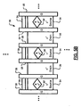
- a transistor 50 according to the present invention is shown to include one or more sources 54 and one or more drains 56.
- the sources 54 and the drains 56 include n + regions. While an NMOS transistor is shown, skilled artisans will appreciate that the present invention also applies to other types of transistors such as PMOS transistors.
- Gates 58 are located between adjacent pairs of sources 54 and drains 56. In one implementation, the gates 58 that are located on opposite sides of the sources 54 are connected together as shown at 64. In other configurations, however, the gates 58 need not be connected together.
- a body 66 including a p + region is arranged inside of and is surrounded by the source 54.
- the body 66 preferably has a shape that tapers as a distance between a midportion of the body 66 and adjacent gates decreases.
- the body 66 may touch or not touch the gates 58 in the plan views of FIGs. 5A and 5B .
- one or both edges of the body 66 may be spaced from the gates 58 in plan view (as shown in FIG. 5A ) and/or substantially aligns with the gates in plan view (as shown in FIG. 5B ).
- the body 66 has a diamond shape.
- FIGs. 6 and 7 other exemplary shapes for the body 66 are shown.
- the body 66 has a hexagon shape.
- the body is generally football shaped.
- Skilled artisans will appreciate that there are a wide variety of other suitable shapes.
- a circular body is shown in FIG. 8 , which is described.
- Other suitable shapes include an ellipse, an octagon, etc.
- the gates 58 can be arranged such that they are closer together when there are no contact taps and further apart when there are contact taps.
- a source contact tap 70 which is not located in the body 66, is located in a region where the adjacent gates 58 are located farther apart.
- a body contact tap 80 which is located in the body 66, is located in the source 54 where the adjacent gates 58 are located farther apart.
- the transistor 120 includes a gate contact 122, a source contact 126, a drain contact 128 and a negative (N)-well contact 130.
- the source contact 126 provides a connection to a P++ region 134 formed an N-type substrate layer 138.
- the N-type layer 138 is formed in a P-type substrate 140.
- the P++ region 134 forms the source.
- the drain contact 128 provides an electrical connection to a P++ region 136 formed in the N-type layer 138.
- the P++ region 136 forms the drain.
- the N-well contact 130 provides a connection to an N++ region 141 or N-well.
- FIG. 11 a plan view of a sixth exemplary layout is shown.
- ESD electrostatic discharge
- the N-well contact area may be approximately 2.5 to 3 times the area in NMOS transistors.
- the source-drain resistance may be less important. Therefore, the layout in FIG. 11 minimizes the N-well contact areas and the source-drain area.
- Skilled artisans will appreciate that while the foregoing description relates to PMOS transistors, similar principles apply to NMOS transistors.
- gate regions 200-1, 200-2, ..., and 200-G are defined between source regions 224-1, 224-2, ..., and 224-S (collectively source regions 224) and drain regions 220-1, 220-2, ..., and 220-D (collectively drain regions 220).
- Adjacent gates 200-1 and 200-2 define regions 210 having a wider width than adjacent regions 212 having narrower widths. Drain regions 220 and source regions 224 are alternately defined between the adjacent gates 200.
- Groups of transistors 230-11, 230-12, ..., and 230-XY are arranged adjacent to each other. Adjacent groups of transistors 230 share R N-well contacts 260, where R is an integer greater than one. The R N-well contacts 260 can be located between the adjacent groups of transistors 230 in regions 210 where the gates 200 are spaced further apart.
- each group may include 4-6 transistors.
- the R N-well contacts 260 are provided for adjacent groups in both vertical and horizontal directions. Therefore, abutting edges of the adjacent groups without the R N-well contacts 260 can be located in regions 212 where the gates are spaced closer together. In other words, the gates 200 can be arranged closer together to minimize areas of the regions 212 without the R N-well contacts 260.
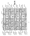
- FIG. 12A an exemplary high-density layout for laterally diffused MOSFET (LDMOS) transistors 300 is shown.
- the layout tends to reduce turn-on drain-source resistance R DSon .
- the transistors 300 include source (S) regions 304, drain (D) regions 306 and gates 310. Some, none or all of the source regions 304 may include one or more source contacts 311. For illustration purposes, not all of the source regions 304 are shown with source contacts 311.
- Source regions 304 are arranged along sides of the drain regions 306. More particularly, the drain regions 306 may have a generally rectangular shape. The source regions 304 may be arranged along each side of the generally rectangular drain regions 306. Substrate contacts 330 may be provided adjacent to corners of the drain regions 306 at intersections between adjacent source regions 304. Drain contacts 334 may also be provided at a central location within the drain regions 306.
- Each drain region 306 may be arranged adjacent to source regions 304 that are common with other adjacent drain regions 306. For example in dotted area 331 in FIG. 12A , drain region 306-1 shares the source region 304-1 with the drain region 306-2. Drain region 306-1 shares the source region 304-2 with the drain region 306-3. Drain region 306-1 shares the source region 304-3 with the drain region 306-4. Drain region 306-1 shares the source region 304-4 with the drain region 306-5. This pattern may be repeated for adjacent drain regions 306.
- Each of the drain regions 306 may have an area that is greater than or equal to two times the area of each of the source regions 304.
- the drain regions 306 have a width "b" and a height "a”.
- the source regions 304 have a width (or height) "d” and a height (or width) "c”.
- the drain regions 306 may have substantially the same length as the source regions 304.
- the drain regions 306 may have greater than or equal to two times the width of the source regions 304.
- Drain contacts 334-1 and 334-3 may be associated with drain regions 306-1 and 306-3, respectively.
- Substrate contacts 330 are located adjacent to corners of the drain regions 306-1.
- Source contacts 311-1, 311-2, ... and 311-B may be arranged in source regions 304-2 and 304-4, where B is an integer.
- Drain contacts 334-1 and 334-3 may be arranged in each of the drain regions 306-1 and 306-3, respectively. Drain contact 334-1 may define an area that is greater than the area of the source contact 311-1 in the source region 304-2.
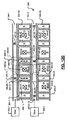
- FIG. 12C another exemplary high-density layout for laterally diffused MOSFET (LDMOS) transistors 340 is shown.
- the layout tends to provide low turn-on drain-source resistance R DSon .
- the transistors 340 include source regions 304-11, 304-12, ... 304-4Q, drain regions 306-11, 306-12, ... 306-4T and gates 310, where Q and T are integers. While four rows are shown in FIG. 12B , additional and/or fewer rows and/or columns may be employed. Some, none or all of the source regions 304 may include source contacts 311. For illustration purposes, not all of the source regions 304 are shown with source contacts. For example, source region 304-12 includes source contacts 311-1, 311-2, ... and 311-B, where B is an integer.
- elongated source regions 344-1, 344-2, 344-3, ... and 344-R are arranged between rows (or columns) of drain regions 306 and may be driven by drivers 346-1, 346-2, ..., and 346-R arranged on one or both sides (or tops) of the layout in FIG. 12B .
- the elongated source regions 344-1, 344-2, 344-3, ... and 344-R may extend adjacent to sides of at least two drain regions 306 such as at least drain regions 306-11 and 306-12.
- Each of the drain regions 306 may have an area that is greater than or equal to two times the area of each of the source regions 304 (such as source region 304-12).
- the drain regions 306 may have substantially the same length as the source regions 304 (such as source region 304-12).
- the drain regions 306 (such as drain region 306-11) may have greater than or equal to two times the width of the source regions 304 (such as source region 304-12).
- Substrate contacts 347-11, 347-12, 347-21, 347-22, 347-23, ... 347-51, 347-52 may be arranged in some, none or all of the elongated source regions 344.
- the placement and number of substrate contracts 347 may be uniform or varied for each of the elongated source regions 344.
- the substrate contacts 347 shown in FIG. 12C may be offset from the substrate contacts 347 in adjacent elongated source regions 344.
- Each of the elongated source regions 344 may include the same number or a different number of substrate contacts 347 than adjacent elongated source regions 344.
- the substrate contacts 347 may be aligned or offset as shown. Some elongated source regions 344 may include no substrate contacts 347. Still other variations are contemplated.
- first areas 345-A1, 345-A2, 345-A3 and 345-A4 may provide useful transistor areas.
- first areas 345-A1, 345-A2, 345-A3 and 345-A4 may be located between drain region 306-12 and source regions 304-12, 344-1, 304-13, and 344-2, respectively.
- Second areas 345-B1, 345-B2, 345-B3 and 345-B4 may provide less useful transistor areas.
- second areas 345-B1, 345-B2, 345-B3 and 345-B4 may be located between source regions 304-12, 344-1, 304-13, and 344-2.
- the substrate contacts 347-11, 347-12, 347-21, 347-22, 347-23, ... may be arranged in some, none or all of the second areas 345-B1, 345-B2, 345-B3 and 345-B4 of the source regions 344-1, 344-2, ... and 344-R, for example as shown in FIG. 12D .
- the substrate contacts 347-11, 347-12, 347-21, 347-22, 347-23, ... are shown arranged in the elongated substrate regions 344-1 and 344-2 and tend to lower R DS_ON .
- the source regions 304 may have a height that is less than or equal to a width "c" of the source regions 304 (as shown in FIG. 12A ) and a width that is less than or equal to a width "d" of the source regions 304 (as shown in FIG. 12A ).
- substrate contacts 330-1 and 330-2 are provided between pairs of elongated source regions 344-1 A and 344-1 B and 344-2A and 344-2B, respectively.
- the elongated source regions 344-1A and 344-2A are driven from one side by drivers 346-1 A and 346-2A.
- the elongated source regions 344-1 B and 344-2B are driven from another side by drivers 346-1B and 346-2B.
- Drain contacts 334 in FiGs. 12A-12E may have a minimum size or a size that is greater than the minimum size. Drain contacts 334 may have a simple or regular shape and/or an irregular or complex shape.
- the drain contacts 334 may have a square or rectangular shape (as shown at 344 in FIG. 12A ), a cross shape (as shown at 344-W in FIG. 12F ), clover-leaf shapes (as shown at 334-X and 334-Y in FIGS. 12G and 12H , respectively), a modified cross-shaped region (as shown at 334-Z in FIG. 12I ) and/or other suitable shapes such as but not limited to diamond, circular, symmetric, non-symmetric, etc..
- the substrate contacts 347 may similarly have a simple or regular shape and/or an irregular or complex shape similar to the drain contacts 334.
- the number of source contacts B in a given source region may be an integer that is greater than one and less than six.
- B may be equal to 3 or 4.
- the area of the drain contact 334-3 may be greater than or equal to 2*B* (the area one of source contacts 311-1, 311-2, ... or 311-B).
- the drain contact region 334-3 may have an area that is approximately greater than or equal to 6 times an area of one source contact 311-1, 311-2, ... or 311-B.
- the drain contact region 334-3 may an area that is approximately greater than or equal to 8 times an area of one source contact 311-1, 311-2, ... or 311-B.
- the complex shapes in FiGs. 12F-12I and/or other complex shapes can be employed for the drain contacts 334.
- the drain contacts 334 can employ deep implant ions in and/or below the drain contacts 334.
- a relief area may be provided in one or both sides of the source region 344 in areas 345-B1, 345-B2, 345-B3 and 345-B.
- a substrate contact region 330 can be positioned in the relief area.
- the shape of the elongate source region 344 can be adjusted on an opposite side of the relief area to offset the effect of the relief area and to prevent reduction in current density in areas of the elongate source region 344 near the relief areas.
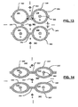
- drain, source and gate regions can also have other shapes that can be used to minimize R DSON .
- drain regions 348 can have a circular shape as shown in FIG. 13 , an elliptical shape as shown in FIG. 14 and/or other suitable shapes.
- Gate regions 349 include circular-shaped gate regions 350 that are connected by linear gate connecting regions 352. Similar elements are identified in FIG. 14 using a prime symbol ("'").
- the drain regions 348 are located in the circular-shaped gate regions 350.
- Source regions 360 are located in between the gate regions 349 in areas other than the inside of the circular shaped gate regions 350.
- Substrate contacts 364 are located in the source regions 360.
- the drain regions 348 may also include a contact region 366.
- the linear gate regions 352 may have a vertical spacing "g" that is minimized to increase density. Likewise, lateral spacing identified at "f" between adjacent circular-shaped gate regions 350 may be minimized to increase density.
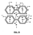
- Drain areas 368 can also have polygon shapes.
- the drain areas can have a hexagon shape as shown in FIG. 15 , although other polygon shapes can be used.
- Gate regions 369 include hexagon-shaped gate regions 370 that are connected by linear gate connecting regions 372.
- the drain regions 368 are located in the hexagon-shaped gate regions 370.
- Source regions 380 are located in between the gate regions 369 in areas other than the inside of the hexagon-shaped gate regions 370.
- Substrate contacts 384 are located in the source regions 380.
- the drain regions may also include a contact region 386.
- the linear gate connecting regions 372 preferably have a vertical spacing "j" that is minimized to increase density. Likewise lateral spacing identified at "i" between adjacent hexagon-shaped gate regions 370 is minimized to increase density.
- the shapes for the drain and gate areas in FIGs. 13-15 can be any shape that is symmetric about at least one of the horizontal and vertical centerlines of the drain areas.
- the transistors in FIGs. 13-15 may be LDMOS transistors.
- the shape of the drain regions may include any symmetric shape. The shape may taper as a distance from a center point of the drain area increases and/or as a center point of the drain area increases in a direction towards one or more other transistors.
- the teachings of the disclosure can be implemented in transistors of a hard disk drive (HDD).
- the HDD includes a hard disk assembly (HDA) and a HDD PCB.
- the HDA may include a magnetic medium, such as one or more platters that store data, and a read/write device.
- the read/write device may be arranged on an actuator arm and may read and write data on the magnetic medium.
- the HDA includes a spindle motor that rotates the magnetic medium and a voice-coil motor (VCM) that actuates the actuator arm.
- VCM voice-coil motor
- a preamplifier device amplifies signals generated by the read/write device during read operations and provides signals to the read/write device during write operations.
- the HDD PCB includes a read/write channel module (hereinafter, "read channel"), a hard disk controller (HDC) module, a buffer, nonvolatile memory, a processor, and a spindle/VCM driver module.
- the read channel processes data received from and transmitted to the preamplifier device.
- the HDC module controls components of the HDA and communicates with an external device (not shown) via an I/O interface.
- the external device may include a computer, a multimedia device, a mobile computing device, etc.
- the I/O interface may include wireline and/or wireless communication links.
- the HDC module may receive data from the HDA, the read channel, the buffer, nonvolatile memory, the processor, the spindle/VCM driver module, and/or the I/O interface.
- the processor may process the data, including encoding, decoding, filtering, and/or formatting.
- the processed data may be output to the HDA, the read channel, the buffer, nonvolatile memory, the processor, the spindle/VCM driver module, and/or the I/O interface.
- the HDC module may use the buffer and/or nonvolatile memory to store data related to the control and operation of the HDD.
- the buffer may include DRAM, SDRAM, etc.
- the nonvolatile memory may include flash memory (including NAND and NOR flash memory), phase change memory, magnetic RAM, or multi-state memory, in which each memory cell has more than two states.
- the spindle/VCM driver module controls the spindle motor and the VCM.
- the HDD PCB includes a power supply that provides power to the components of the HDD.
- the teachings of the disclosure can further implemented in transistors of a DVD drive or of a CD drive.
- the DVD drive includes a DVD PCB and a DVD assembly (DVDA).
- the DVD PCB includes a DVD control module, a buffer, nonvolatile memory, a processor 424, a spindle/FM (feed motor) driver module, an analog front-end module, a write strategy module, and a DSP module.
- the DVD control module controls components of the DVDA and communicates with an external device (not shown) via an I/O interface.
- the external device may include a computer, a multimedia device, a mobile computing device, etc.
- the I/O interface may include wireline and/or wireless communication links.
- the DVD control module may receive data from the buffer, nonvolatile memory, the processor, the spindle/FM driver module, the analog front-end module, the write strategy module, the DSP module, and/or the I/O interface.
- the processor may process the data, including encoding, decoding, filtering, and/or formatting.
- the DSP module performs signal processing, such as video and/or audio coding/decoding.
- the processed data may be output to the buffer, nonvolatile memory, the processor, the spindle/FM driver module, the analog front-end module, the write strategy module, the DSP module, and/or the I/O interface.
- the DVD control module may use the buffer and/or nonvolatile memory to store data related to the control and operation of the DVD drive.
- the buffer may include DRAM, SDRAM, etc.
- the nonvolatile memory may include flash memory (including NAND and NOR flash memory), phase change memory, magnetic RAM, or multi-state memory, in which each memory cell has more than two states.
- the DVD PCB includes a power supply that provides power to the components of the DVD drive.
- the DVDA may include a preamplifier device, a laser driver, and an optical device, which may be an optical read/write (ORW) device or an optical read-only (OR) device.
- a spindle motor rotates an optical storage medium, and a feed motor actuates the optical device relative to the optical storage medium.
- the laser driver When reading data from the optical storage medium, the laser driver provides a read power to the optical device.
- the optical device detects data from the optical storage medium, and transmits the data to the preamplifier device.
- the analog front-end module receives data from the preamplifier device and performs such functions as filtering and A/D conversion.
- the write strategy module transmits power level and timing information to the laser driver.
- the laser driver controls the optical device to write data to the optical storage medium.
- the teachings of the disclosure can further be implemented in a transistors of a high definition television (HDTV).
- the HDTV includes a HDTV control module, a display, a power supply, memory, a storage device, a WLAN interface and associated antenna 444, and an external interfaces.
- the HDTV can receive input signals from the WLAN interface and/or the external interface, which sends and receives information via cable, broadband Internet, and/or satellite.
- the HDTV control module may process the input signals, including encoding, decoding, filtering, and/or formatting, and generate output signals.
- the output signals may be communicated to one or more of the display, memory, the storage device, the W LAN interface, and the external interface.
- Memory may include random access memory (RAM) and/or nonvolatile memory such as flash memory, phase change memory, or multi-state memory, in which each memory cell has more than two states.
- the storage device may include an optical storage drive, such as a DVD drive, and/or a hard disk drive (HDD).
- the HDTV control module communicates externally via the WLAN interface and/or the external interface.
- the power supply provides power to the components of the HDTV.
- the teachings of the disclosure may be implemented in a transistors of a vehicle.
- the vehicle may include a vehicle control system, a power supply, memory, a storage device, and a WLAN interface and associated antenna.
- the vehicle control system may be a powertrain control system, a body control system, an entertainment control system, an anti-lock braking system (ABS), a navigation system, a telematics system, a lane departure system, an adaptive cruise control system, etc.
- the vehicle control system may communicate with one or more sensors and generate one or more output signals.
- the sensors may include temperature sensors, acceleration sensors, pressure sensors, rotational sensors, airflow sensors, etc.
- the output signals may control engine operating parameters, transmission operating parameters, suspension parameters, etc.
- the power supply provides power to the components of the vehicle.
- the vehicle control system 447 may store data in Memory and/or the storage device.
- Memory may include random access memory (RAM) and/or nonvolatile memory such as flash memory, phase change memory, or multi-state memory, in which each memory cell has more than two states.
- the storage device may include an optical storage drive, such as a DVD drive, and/or a hard disk drive (HDD).
- the vehicle control system may communicate externally using the WLAN interface.
- the teachings of the disclosure can further be implemented in a transistors of a cellular phone.
- the cellular phone includes a phone control module, a power supply, memory, a storage device, and a cellular network interface.
- the cellular phone may include a WLAN interface and associated antenna, a microphone, an audio output such as a speaker and/or output jack, a display, and a user input device such as a keypad and/or pointing device.
- the phone control module may receive input signals from the cellular network interface, the WLAN interface, the microphone, and/or the user input device.
- the phone control module may process signals, including encoding, decoding, filtering, and/or formatting, and generate output signals.
- the output signals may be communicated to one or more of memory, the storage device, the cellular network interface, the WLAN interface, and the audio.
- Memory may include random access memory (RAM) and/or nonvolatile memory such as flash memory, phase change memory, or multi-state memory, in which each memory cell has more than two states.
- the storage device may include an optical storage drive, such as a DVD drive, and/or a hard disk drive (HDD).
- the power supply 462 provides power to the components of the cellular phone.
- the teachings of the disclosure can further be implemented in a transistors of a set top box.
- the set top box includes a set top control module, a display, a power supply, memory, a storage device, and a WLAN interface and associated antenna.
- the set top control module may receive input signals from the WLAN interface and an external interface, which can send and receive information via cable, broadband Internet, and/or satellite.
- the set top control module may process signals, including encoding, decoding, filtering, and/or formatting, and generate output signals.
- the output signals may include audio and/or video signals in standard and/or high definition formats.
- the output signals may be communicated to the WLAN interface and/or to the display.
- the display may include a television, a projector, and/or a monitor.
- the power supply provides power to the components of the set top box.
- Memory may include random access memory (RAM) and/or nonvolatile memory such as flash memory, phase change memory, or multi-state memory, in which each memory cell has more than two states.
- RAM random access memory
- nonvolatile memory such as flash memory, phase change memory, or multi-state memory, in which each memory cell has more than two states.
- the storage device may include an optical storage drive, such as a DVD drive, and/or a hard disk drive (HDD).
- HDD hard disk drive
- the teachings of the disclosure can further be implemented in a transistors of a media player.
- the media player may include a media player control module, a power supply, memory, a storage device, a WLAN interface and associated antenna, and an external interface.
- the media player control module may receive input signals from the WLAN interface and/or the external interface.
- the external interface may include USB, infrared, and/or Ethernet.
- the input signals may include compressed audio and/or video, and may be compliant with the MP3 format. Additionally, the media player control module may receive input from a user input such as a keypad, touchpad, or individual buttons.
- the media player control module may process input signals, including encoding, decoding, filtering, and/or formatting, and generate output signals.
- the media player control module may output audio signals to an audio output and video signals to a display.
- the audio output may include a speaker and/or an output jack.
- the display may present a graphical user interface, which may include menus, icons, etc.
- the power supply provides power to the components of the media player.
- Memory may include random access memory (RAM) and/or nonvolatile memory such as flash memory, phase change memory, or multi-state memory, in which each memory cell has more than two states.
- the storage device may include an optical storage drive, such as a DVD drive, and/or a hard disk drive (HDD).
Landscapes
- Metal-Oxide And Bipolar Metal-Oxide Semiconductor Integrated Circuits (AREA)
- Insulated Gate Type Field-Effect Transistor (AREA)
- Semiconductor Integrated Circuits (AREA)
- Electrodes Of Semiconductors (AREA)
- Internal Circuitry In Semiconductor Integrated Circuit Devices (AREA)
- Amplifiers (AREA)
- Thin Film Transistor (AREA)
Applications Claiming Priority (10)
| Application Number | Priority Date | Filing Date | Title |
|---|---|---|---|
| US79856806P | 2006-05-08 | 2006-05-08 | |
| US82100806P | 2006-08-01 | 2006-08-01 | |
| US82333206P | 2006-08-23 | 2006-08-23 | |
| US82435706P | 2006-09-01 | 2006-09-01 | |
| US82551706P | 2006-09-13 | 2006-09-13 | |
| US11/524,113 US7851872B2 (en) | 2003-10-22 | 2006-09-20 | Efficient transistor structure |
| US11/586,467 US7528444B2 (en) | 2003-10-22 | 2006-10-25 | Efficient transistor structure |
| US11/586,471 US7652338B2 (en) | 2003-10-22 | 2006-10-25 | Efficient transistor structure |
| US11/586,470 US7863657B2 (en) | 2003-10-22 | 2006-10-25 | Efficient transistor structure |
| PCT/US2007/011207 WO2007136556A2 (en) | 2006-05-08 | 2007-05-08 | Efficient transistor structure |
Publications (2)
| Publication Number | Publication Date |
|---|---|
| EP2030237A2 EP2030237A2 (en) | 2009-03-04 |
| EP2030237B1 true EP2030237B1 (en) | 2011-02-09 |
Family
ID=38723776
Family Applications (1)
| Application Number | Title | Priority Date | Filing Date |
|---|---|---|---|
| EP07809055A Ceased EP2030237B1 (en) | 2006-05-08 | 2007-05-08 | Efficient transistor structure |
Country Status (6)
| Country | Link |
|---|---|
| EP (1) | EP2030237B1 (https=) |
| JP (1) | JP5137947B2 (https=) |
| KR (1) | KR101373792B1 (https=) |
| CN (1) | CN101490843B (https=) |
| TW (4) | TWI407566B (https=) |
| WO (1) | WO2007136556A2 (https=) |
Cited By (1)
| Publication number | Priority date | Publication date | Assignee | Title |
|---|---|---|---|---|
| EP2100334B1 (en) * | 2006-12-28 | 2016-04-13 | Marvell World Trade Ltd. | Geometry of mos device with low on-resistance |
Families Citing this family (5)
| Publication number | Priority date | Publication date | Assignee | Title |
|---|---|---|---|---|
| CN102623496B (zh) * | 2011-01-27 | 2014-11-05 | 无锡华润上华半导体有限公司 | 矩阵型mos场效应晶体管 |
| JP5586546B2 (ja) * | 2011-03-23 | 2014-09-10 | 株式会社東芝 | 半導体装置 |
| US11195794B2 (en) * | 2020-02-05 | 2021-12-07 | Samsung Electronics Co., Ltd. | Stacked integrated circuit devices including a routing wire |
| CN111599862A (zh) * | 2020-05-21 | 2020-08-28 | Oppo广东移动通信有限公司 | 晶体管以及集成电路 |
| DE112021003691T5 (de) * | 2020-07-10 | 2023-04-20 | Sony Group Corporation | Ansteuerungsschaltkreisarraysubstrat, anzeigevorrichtung und elektronische einrichtung |
Family Cites Families (24)
| Publication number | Priority date | Publication date | Assignee | Title |
|---|---|---|---|---|
| US4409499A (en) * | 1982-06-14 | 1983-10-11 | Standard Microsystems Corporation | High-speed merged plane logic function array |
| JPS6076160A (ja) * | 1983-10-03 | 1985-04-30 | Seiko Epson Corp | 半導体集積回路 |
| JPH01207976A (ja) * | 1988-02-15 | 1989-08-21 | Nec Corp | 半導体装置 |
| CA2046554A1 (en) * | 1990-07-10 | 1992-01-11 | Masahiro Kugishima | Basic cell and arrangement structure thereof |
| JPH07161984A (ja) * | 1993-12-06 | 1995-06-23 | Mitsubishi Electric Corp | 半導体集積回路装置 |
| JPH07283377A (ja) * | 1994-01-03 | 1995-10-27 | Texas Instr Inc <Ti> | 小型ゲートアレイおよびその製造方法 |
| JP2611687B2 (ja) * | 1995-06-26 | 1997-05-21 | セイコーエプソン株式会社 | 半導体装置 |
| US5838050A (en) * | 1996-06-19 | 1998-11-17 | Winbond Electronics Corp. | Hexagon CMOS device |
| US6236258B1 (en) * | 1998-08-25 | 2001-05-22 | International Business Machines Corporation | Wordline driver circuit using ring-shaped devices |
| JP2000208759A (ja) * | 1999-01-12 | 2000-07-28 | Rohm Co Ltd | 半導体装置 |
| DE19958906A1 (de) * | 1999-12-07 | 2001-07-05 | Infineon Technologies Ag | Herstellung von integrierten Schaltungen |
| JP2001339047A (ja) * | 2000-05-29 | 2001-12-07 | Matsushita Electric Ind Co Ltd | 半導体装置 |
| TW447129B (en) * | 2000-06-30 | 2001-07-21 | United Microelectronics Corp | Array type SOI transistor layout |
| JP4124981B2 (ja) * | 2001-06-04 | 2008-07-23 | 株式会社ルネサステクノロジ | 電力用半導体装置および電源回路 |
| US6566710B1 (en) * | 2001-08-29 | 2003-05-20 | National Semiconductor Corporation | Power MOSFET cell with a crossed bar shaped body contact area |
| US6724044B2 (en) * | 2002-05-10 | 2004-04-20 | General Semiconductor, Inc. | MOSFET device having geometry that permits frequent body contact |
| JP5179692B2 (ja) * | 2002-08-30 | 2013-04-10 | 富士通セミコンダクター株式会社 | 半導体記憶装置及びその製造方法 |
| US7079829B2 (en) * | 2002-11-15 | 2006-07-18 | Matsushita Electric Industrial Co, Ltd. | Semiconductor differential circuit, oscillation apparatus, switching apparatus, amplifying apparatus, mixer apparatus and circuit apparatus using same, and semiconductor differential circuit placement method |
| KR100485174B1 (ko) | 2002-12-24 | 2005-04-22 | 동부아남반도체 주식회사 | 모스 트랜지스터 제조 방법 |
| JP3708082B2 (ja) * | 2003-02-27 | 2005-10-19 | 株式会社ルネサステクノロジ | 電力半導体装置 |
| US7091565B2 (en) * | 2003-10-22 | 2006-08-15 | Marvell World Trade Ltd. | Efficient transistor structure |
| TWI241720B (en) * | 2004-01-16 | 2005-10-11 | Super Nova Optoelectronics Cor | Replaceable light emitting diode packaging structure |
| JP2005311131A (ja) * | 2004-04-22 | 2005-11-04 | Toshiba Corp | 不揮発性半導体記憶装置及びその製造方法 |
| JP2007258314A (ja) * | 2006-03-22 | 2007-10-04 | Seiko Npc Corp | 半導体装置の製造方法及び半導体装置 |
-
2007
- 2007-05-08 TW TW096116397A patent/TWI407566B/zh not_active IP Right Cessation
- 2007-05-08 EP EP07809055A patent/EP2030237B1/en not_active Ceased
- 2007-05-08 WO PCT/US2007/011207 patent/WO2007136556A2/en not_active Ceased
- 2007-05-08 KR KR1020087029444A patent/KR101373792B1/ko not_active Expired - Fee Related
- 2007-05-08 TW TW096116398A patent/TWI429078B/zh not_active IP Right Cessation
- 2007-05-08 TW TW096116400A patent/TWI420665B/zh not_active IP Right Cessation
- 2007-05-08 CN CN2007800259194A patent/CN101490843B/zh not_active Expired - Fee Related
- 2007-05-08 TW TW096116401A patent/TW200805663A/zh unknown
- 2007-05-08 JP JP2009509836A patent/JP5137947B2/ja not_active Expired - Fee Related
Cited By (2)
| Publication number | Priority date | Publication date | Assignee | Title |
|---|---|---|---|---|
| EP2100334B1 (en) * | 2006-12-28 | 2016-04-13 | Marvell World Trade Ltd. | Geometry of mos device with low on-resistance |
| US9466596B2 (en) | 2006-12-28 | 2016-10-11 | Marvell World Trade Ltd. | Geometry of MOS device with low on-resistance |
Also Published As
| Publication number | Publication date |
|---|---|
| TW200802870A (en) | 2008-01-01 |
| KR20090013219A (ko) | 2009-02-04 |
| CN101490843A (zh) | 2009-07-22 |
| WO2007136556A2 (en) | 2007-11-29 |
| TW200802869A (en) | 2008-01-01 |
| JP5137947B2 (ja) | 2013-02-06 |
| TWI429078B (zh) | 2014-03-01 |
| TWI407566B (zh) | 2013-09-01 |
| WO2007136556A3 (en) | 2008-07-03 |
| TW200805662A (en) | 2008-01-16 |
| TWI420665B (zh) | 2013-12-21 |
| CN101490843B (zh) | 2011-01-26 |
| WO2007136556B1 (en) | 2008-08-28 |
| EP2030237A2 (en) | 2009-03-04 |
| TW200805663A (en) | 2008-01-16 |
| JP2009536789A (ja) | 2009-10-15 |
| KR101373792B1 (ko) | 2014-03-13 |
Similar Documents
| Publication | Publication Date | Title |
|---|---|---|
| US7528444B2 (en) | Efficient transistor structure | |
| CN102709285B (zh) | 具有低导通电阻的mos器件的几何图形 | |
| US9373392B2 (en) | Memory cells with rectifying device | |
| EP2030237B1 (en) | Efficient transistor structure | |
| CN112713150B (zh) | 存储器阵列及用于形成包括存储器单元串的存储器阵列的方法 | |
| US6864518B1 (en) | Bit cells having offset contacts in a memory array | |
| US20250098217A1 (en) | Gate-all-around field effect transistor structures | |
| US20250096130A1 (en) | Gate-all-around field effect transistor structures | |
| US20250248100A1 (en) | Variable stack nanosheet devices and methods for making the same | |
| US20250096075A1 (en) | Memory cell structures using full backside connectivity | |
| US20250098302A1 (en) | Compact logic cells using full backside connectivity | |
| CN118235533A (zh) | 包括存储器单元串的存储器阵列及用于形成包括存储器单元串的存储器阵列的方法 |
Legal Events
| Date | Code | Title | Description |
|---|---|---|---|
| PUAI | Public reference made under article 153(3) epc to a published international application that has entered the european phase |
Free format text: ORIGINAL CODE: 0009012 |
|
| 17P | Request for examination filed |
Effective date: 20081205 |
|
| AK | Designated contracting states |
Kind code of ref document: A2 Designated state(s): DE FR GB |
|
| 17Q | First examination report despatched |
Effective date: 20090403 |
|
| DAX | Request for extension of the european patent (deleted) | ||
| RBV | Designated contracting states (corrected) |
Designated state(s): DE FR GB |
|
| GRAP | Despatch of communication of intention to grant a patent |
Free format text: ORIGINAL CODE: EPIDOSNIGR1 |
|
| GRAC | Information related to communication of intention to grant a patent modified |
Free format text: ORIGINAL CODE: EPIDOSCIGR1 |
|
| GRAS | Grant fee paid |
Free format text: ORIGINAL CODE: EPIDOSNIGR3 |
|
| GRAA | (expected) grant |
Free format text: ORIGINAL CODE: 0009210 |
|
| AK | Designated contracting states |
Kind code of ref document: B1 Designated state(s): DE FR GB |
|
| REG | Reference to a national code |
Ref country code: GB Ref legal event code: FG4D |
|
| REF | Corresponds to: |
Ref document number: 602007012434 Country of ref document: DE Date of ref document: 20110324 Kind code of ref document: P |
|
| REG | Reference to a national code |
Ref country code: DE Ref legal event code: R096 Ref document number: 602007012434 Country of ref document: DE Effective date: 20110324 |
|
| PLBE | No opposition filed within time limit |
Free format text: ORIGINAL CODE: 0009261 |
|
| STAA | Information on the status of an ep patent application or granted ep patent |
Free format text: STATUS: NO OPPOSITION FILED WITHIN TIME LIMIT |
|
| 26N | No opposition filed |
Effective date: 20111110 |
|
| REG | Reference to a national code |
Ref country code: DE Ref legal event code: R097 Ref document number: 602007012434 Country of ref document: DE Effective date: 20111110 |
|
| REG | Reference to a national code |
Ref country code: FR Ref legal event code: PLFP Year of fee payment: 10 |
|
| REG | Reference to a national code |
Ref country code: FR Ref legal event code: PLFP Year of fee payment: 11 |
|
| REG | Reference to a national code |
Ref country code: FR Ref legal event code: PLFP Year of fee payment: 12 |
|
| PGFP | Annual fee paid to national office [announced via postgrant information from national office to epo] |
Ref country code: DE Payment date: 20180529 Year of fee payment: 12 |
|
| PGFP | Annual fee paid to national office [announced via postgrant information from national office to epo] |
Ref country code: FR Payment date: 20180525 Year of fee payment: 12 |
|
| PGFP | Annual fee paid to national office [announced via postgrant information from national office to epo] |
Ref country code: GB Payment date: 20180529 Year of fee payment: 12 |
|
| REG | Reference to a national code |
Ref country code: DE Ref legal event code: R119 Ref document number: 602007012434 Country of ref document: DE |
|
| GBPC | Gb: european patent ceased through non-payment of renewal fee |
Effective date: 20190508 |
|
| PG25 | Lapsed in a contracting state [announced via postgrant information from national office to epo] |
Ref country code: GB Free format text: LAPSE BECAUSE OF NON-PAYMENT OF DUE FEES Effective date: 20190508 Ref country code: DE Free format text: LAPSE BECAUSE OF NON-PAYMENT OF DUE FEES Effective date: 20191203 |
|
| PG25 | Lapsed in a contracting state [announced via postgrant information from national office to epo] |
Ref country code: FR Free format text: LAPSE BECAUSE OF NON-PAYMENT OF DUE FEES Effective date: 20190531 |