EP2019332A1 - Procédé de génération de données de photomasques, procédé de génération de photomasques, procédé d'exposition, et procédé de fabrication du dispositif - Google Patents
Procédé de génération de données de photomasques, procédé de génération de photomasques, procédé d'exposition, et procédé de fabrication du dispositif Download PDFInfo
- Publication number
- EP2019332A1 EP2019332A1 EP08161096A EP08161096A EP2019332A1 EP 2019332 A1 EP2019332 A1 EP 2019332A1 EP 08161096 A EP08161096 A EP 08161096A EP 08161096 A EP08161096 A EP 08161096A EP 2019332 A1 EP2019332 A1 EP 2019332A1
- Authority
- EP
- European Patent Office
- Prior art keywords
- pattern
- original plate
- optical system
- projection optical
- generating
- Prior art date
- Legal status (The legal status is an assumption and is not a legal conclusion. Google has not performed a legal analysis and makes no representation as to the accuracy of the status listed.)
- Granted
Links
- 238000000034 method Methods 0.000 title claims abstract description 52
- 238000004519 manufacturing process Methods 0.000 title claims description 7
- 230000003287 optical effect Effects 0.000 claims abstract description 86
- 238000005286 illumination Methods 0.000 claims abstract description 41
- 238000012545 processing Methods 0.000 claims abstract description 29
- 210000001747 pupil Anatomy 0.000 claims abstract description 26
- 238000009826 distribution Methods 0.000 claims abstract description 18
- 230000005540 biological transmission Effects 0.000 claims abstract description 12
- 239000000758 substrate Substances 0.000 claims description 34
- 230000006870 function Effects 0.000 description 69
- 238000004364 calculation method Methods 0.000 description 34
- 230000014509 gene expression Effects 0.000 description 21
- 230000010287 polarization Effects 0.000 description 21
- 238000003860 storage Methods 0.000 description 21
- 230000004075 alteration Effects 0.000 description 14
- 230000001427 coherent effect Effects 0.000 description 14
- 238000012546 transfer Methods 0.000 description 12
- 230000004907 flux Effects 0.000 description 9
- 230000000873 masking effect Effects 0.000 description 8
- 230000010354 integration Effects 0.000 description 7
- 230000015572 biosynthetic process Effects 0.000 description 6
- 230000008569 process Effects 0.000 description 6
- 239000004065 semiconductor Substances 0.000 description 6
- 238000004088 simulation Methods 0.000 description 6
- 238000007796 conventional method Methods 0.000 description 5
- 239000007788 liquid Substances 0.000 description 5
- 238000007493 shaping process Methods 0.000 description 5
- 239000011651 chromium Substances 0.000 description 4
- 230000000694 effects Effects 0.000 description 4
- 238000003384 imaging method Methods 0.000 description 4
- 239000000463 material Substances 0.000 description 4
- 238000010894 electron beam technology Methods 0.000 description 3
- 239000004973 liquid crystal related substance Substances 0.000 description 3
- 230000010363 phase shift Effects 0.000 description 3
- 230000008859 change Effects 0.000 description 2
- 238000011960 computer-aided design Methods 0.000 description 2
- 238000000354 decomposition reaction Methods 0.000 description 2
- 238000001459 lithography Methods 0.000 description 2
- 230000007246 mechanism Effects 0.000 description 2
- 238000012544 monitoring process Methods 0.000 description 2
- 230000009467 reduction Effects 0.000 description 2
- VYZAMTAEIAYCRO-UHFFFAOYSA-N Chromium Chemical compound [Cr] VYZAMTAEIAYCRO-UHFFFAOYSA-N 0.000 description 1
- 241000276498 Pollachius virens Species 0.000 description 1
- 229910052804 chromium Inorganic materials 0.000 description 1
- 238000012937 correction Methods 0.000 description 1
- 230000003247 decreasing effect Effects 0.000 description 1
- 238000005530 etching Methods 0.000 description 1
- 239000011521 glass Substances 0.000 description 1
- 238000007654 immersion Methods 0.000 description 1
- 238000009434 installation Methods 0.000 description 1
- 238000012804 iterative process Methods 0.000 description 1
- 238000013178 mathematical model Methods 0.000 description 1
- 238000005259 measurement Methods 0.000 description 1
- 238000012986 modification Methods 0.000 description 1
- 230000004048 modification Effects 0.000 description 1
- 238000004806 packaging method and process Methods 0.000 description 1
- 229920002120 photoresistant polymer Polymers 0.000 description 1
- 230000004044 response Effects 0.000 description 1
- 238000001228 spectrum Methods 0.000 description 1
- 230000001360 synchronised effect Effects 0.000 description 1
- 239000010409 thin film Substances 0.000 description 1
Images


Classifications
-
- G—PHYSICS
- G03—PHOTOGRAPHY; CINEMATOGRAPHY; ANALOGOUS TECHNIQUES USING WAVES OTHER THAN OPTICAL WAVES; ELECTROGRAPHY; HOLOGRAPHY
- G03F—PHOTOMECHANICAL PRODUCTION OF TEXTURED OR PATTERNED SURFACES, e.g. FOR PRINTING, FOR PROCESSING OF SEMICONDUCTOR DEVICES; MATERIALS THEREFOR; ORIGINALS THEREFOR; APPARATUS SPECIALLY ADAPTED THEREFOR
- G03F1/00—Originals for photomechanical production of textured or patterned surfaces, e.g., masks, photo-masks, reticles; Mask blanks or pellicles therefor; Containers specially adapted therefor; Preparation thereof
- G03F1/36—Masks having proximity correction features; Preparation thereof, e.g. optical proximity correction [OPC] design processes
-
- G—PHYSICS
- G03—PHOTOGRAPHY; CINEMATOGRAPHY; ANALOGOUS TECHNIQUES USING WAVES OTHER THAN OPTICAL WAVES; ELECTROGRAPHY; HOLOGRAPHY
- G03F—PHOTOMECHANICAL PRODUCTION OF TEXTURED OR PATTERNED SURFACES, e.g. FOR PRINTING, FOR PROCESSING OF SEMICONDUCTOR DEVICES; MATERIALS THEREFOR; ORIGINALS THEREFOR; APPARATUS SPECIALLY ADAPTED THEREFOR
- G03F7/00—Photomechanical, e.g. photolithographic, production of textured or patterned surfaces, e.g. printing surfaces; Materials therefor, e.g. comprising photoresists; Apparatus specially adapted therefor
- G03F7/70—Microphotolithographic exposure; Apparatus therefor
- G03F7/70425—Imaging strategies, e.g. for increasing throughput or resolution, printing product fields larger than the image field or compensating lithography- or non-lithography errors, e.g. proximity correction, mix-and-match, stitching or double patterning
- G03F7/70433—Layout for increasing efficiency or for compensating imaging errors, e.g. layout of exposure fields for reducing focus errors; Use of mask features for increasing efficiency or for compensating imaging errors
- G03F7/70441—Optical proximity correction [OPC]
Definitions
- the present invention generally relates to an original plate data generation method, an original plate generation method, and an exposure method.
- An exposure apparatus is used in a photolithographic process for manufacturing a semiconductor device such as an integrated circuit (IC).
- An exposure apparatus illuminates an original plate (also referred to as a "mask” or a “reticle”) and exposes a circuit pattern drawn on the original plate onto a substrate (a wafer) via a projection optical system.
- a resolution which indicates how minute a pattern can be formed on the substrate and a throughput which is indicated by a number of substrates that can be completely exposure-processed in a unit of time are used as indexes for the capacity of the exposure apparatus.
- conventional methods increase a driving speed of a stage that supports a substrate or increase an amount of light intensity on a surface of a substrate.
- NA numerical aperture
- a representative conventional method inserts an auxiliary pattern having a size with which the auxiliary pattern is not resolved, into an original plate on which a contact hole pattern to be transferred is drawn. This method is one of the conventional methods for decreasing the k1 factor.
- Japanese Patent Application Laid-Open No. 2004-221594 discusses a method for deriving how an auxiliary pattern is inserted by a numerical calculation.
- the method discussed in Japanese Patent Application Laid-Open No. 2004-221594 obtains a distribution of an approximate image plane intensity (amplitude) by a numerical calculation to derive an interference map indicating the distribution of the approximate image plane intensity (amplitude).
- the method discussed in Japanese Patent Application Laid-Open No. 2004-221594 arranges an auxiliary pattern around a pattern to be transferred using the interference map.
- the present invention is directed to a method for generating original plate data adapted to improve a resolution and a throughput of an exposure apparatus.
- Fig. 1 illustrates a configuration of a computer according to exemplary embodiments of the present invention.
- Fig. 2 is a flow chart illustrating original plate data generation processing according to the exemplary embodiments of the present invention.
- Figs. 3A through 3F illustrate original plate data generation processing according to a first exemplary embodiment of the present invention.
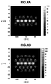
- Figs. 4A and 4B illustrate an aerial image simulation result according to the first exemplary embodiment of the present invention.
- Fig. 5 illustrates a graph showing the result in Figs. 4A and 4B according to the first exemplary embodiment of the present invention.
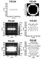
- Figs. 6A through 6F illustrate original plate data generation processing according to a second exemplary embodiment of the present invention.
- Figs. 7A and 7B illustrate an aerial image simulation result according to the second exemplary embodiment of the present invention.
- Fig. 8 illustrates a graph showing the result in Fig. 7A and 7B according to the second exemplary embodiment of the present invention.
- Fig. 9 illustrates an example of a hardware configuration of an exposure apparatus.
- the conception according to an exemplary embodiment of the present invention can be expressed as hardware or put into a mathematical model. Accordingly, an exemplary embodiment of the present invention can be installed in a computer system as a program.
- the software function of the computer system includes a program having computer-executable program codes and can determine a pattern of a mask which is an original plate and generate original plate data.
- the software codes can be stored on at least a storage medium such as a machine-readable medium or a memory, as one or more modules.
- the exemplary embodiment of the present invention which will be described below, can be described in the form of program codes and can function as one or more software products.
- a computer 1 includes a bus 10, a control unit 20, a display unit 30, a storage unit 40, an input unit 60, and a storage medium interface 70.
- the control unit 20, the display unit 30, the storage unit 40, the input unit 60, and the storage medium interface 70 are connected to one another via the bus 10.
- a storage medium 80 can be connected to the storage medium interface 70.
- the storage unit 40 stores pattern data 40a, an interference map 40b, an approximate aerial image 40c, original plate (a mask or a reticle) data 40d, effective light source information 40e, NA information 40f, ⁇ information 40g, aberration information 40h, polarization information 40i, resist information 40j, and an original plate data generation program 40k.
- the pattern data 40a is information about a pattern arranged on a mask surface (an object plane) of the projection optical system.
- the pattern data 40a is necessary for calculating an interference map or an approximate aerial image, which will be described below.
- the pattern data 40a can be data of a pattern whose layout is designed in a designing process of an integrated circuit (IC) (hereinafter referred to as a "layout pattern") itself or a pattern including an auxiliary pattern.
- IC integrated circuit
- the approximate aerial image 40c indicates a distribution of the approximate aerial images on a wafer surface, which will be described below.
- the original plate data 40d is data for drawing a pattern made of chromium (Cr) on the mask surface.
- the effective light source information 40e is information about a distribution of the intensity of light formed on a pupil plane 142 of a projection optical system 140 of an exposure apparatus 100, which will be described below (see Fig. 9 ).
- the effective light source 40e is equivalent to a distribution of an angle of a light flux incident on the mask surface of the projection optical system 140.
- the NA information 40f is information about the number of numerical apertures NA on the image side of the projection optical system 140.
- the ⁇ information 40g is information about a wavelength ⁇ of an exposure light emitted from the exposure apparatus 100.
- the aberration information 40h is information about aberrations occurring in the projection optical system 140.
- a phase shift occurs due to the double refraction.
- the phase shift can be considered as a kind of aberration.
- the polarization information 40i is information about the polarization of the illumination light emitted from an illumination device 110 of the exposure apparatus 100.
- the resist information 40j is information about the photo-sensitive resist to be coated on a wafer.
- the interference map 40b is an interference map discussed in Japanese Patent Application Laid-Open No. 2004-221594 .
- the original plate data generation program 40k is a program for generating data such as an original plate pattern.
- the control unit 20 is a central processing unit (CPU), a graphical processing unit (GPU), a digital signal processor (DSP), or a microcomputer.
- the control unit 20 includes a cache memory for temporarily storing data or information.
- the display unit 30 is a display device such as a cathode ray tube (CRT) display or a liquid crystal display.
- the storage unit 40 is a memory or a hard disk.
- the input unit 60 is an input device such as a keyboard and a pointing device such as a mouse.
- the storage medium interface 70 is a floppy disk drive, a compact disk read only memory (CD-ROM) drive, or a universal serial bus (USB) interface, for example.
- the storage medium 80 is, for example, a floppy disk, a CD-ROM, or a USB memory.
- a method for generating an original plate pattern by arranging an auxiliary pattern using an interference map or an approximate aerial image according to the present exemplary embodiment will be described.
- the dimensions of a pattern on the mask surface and that on the wafer surface differ corresponding to a magnification of the projection optical system 140.
- the dimension of the pattern on the mask surface corresponds one-on-one to that on the wafer surface by multiplying the dimension of the pattern on the mask surface by the magnification. Therefore, a coordinate system for the mask surface corresponds one-on-one to that for the wafer surface.
- the interference map is the Fourier transform of a function indicating a pattern on the mask surface (mask function).
- N' usually has a numerical value "1".
- the resulting value at each position of the interference map indicates a degree of interference between the light from each position and the light reflected from the pattern A.
- the resolution for the pattern A can be improved because the light from each position is intensified with the light from the pattern A. For example, the light from a position at which the value indicated by the interference map is "0" does not interfere with the diffracted light from the pattern A.
- a method for deriving an approximate aerial image will be described.
- a mask pattern and a wafer pattern (image of the mask pattern) in a semiconductor exposure apparatus are in a mutual relationship of a partial coherent image formation.
- the partial coherent image formation can be calculated using the TCC.
- the TCC is generally defined as a coefficient on a pupil plane of a projection optical system. More specifically, the TCC is an overlapped portion among an effective light source, a pupil function of the projection optical system, and a complex conjugate of the pupil function for the projection optical system.
- TCC f ⁇ , g ⁇ , f “ , g “ ⁇ S ( f , g ) P ( f + f ⁇ , g + g ⁇ ) P * f + f “ , g + g " ⁇ dfdg
- S(f, g) denotes a coordinate on the pupil plane
- P(f, g) denotes a pupil function
- * denotes a complex conjugate
- the range of integration is from "- ⁇ " to " ⁇ ".
- the aberration in the projection optical system, the polarization of the illumination light, and the resist information can be included in the pupil function P(f, g). Accordingly, the term "pupil function" used herein can include the polarization, the aberration, and the resist information.
- a (f, g) denotes a function indicating a diffracted light distribution of the pattern on the object plane (the function obtained by Fourier-transforming the pattern on the object plane).
- the expression (4) includes a term similar to a Fourier transform format, and a simple addition is only repeated in the expression (4). It is useful to perform a calculation combining the Fourier transform and an addition loop, as expressed in an expression (5) below by modifying the expression (4) :
- I x ⁇ y ⁇ f ⁇ , g ⁇ a ( f ⁇ , g ⁇ ) exp [ - i ⁇ 2 ⁇ ⁇ ⁇ f ⁇ x + g ⁇ y ] ⁇ F - 1 W f ⁇ , g ⁇ f " , g " ⁇ a * f " , g "
- F -1 denotes the inverse Fourier transform.
- the function "W f', g' (f", g")" is a two-dimensional function, which herein is referred to as a "two-dimensional transmission cross coefficient".
- the two-dimensional transmission cross coefficient "W f', g' (f", g")" is an addition loop, and is re-calculated every time the value for the term (f', g') varies.
- the TCC which is a four-dimensional function as shown in the expression (2), is not necessary and the expression (5) performs only the double loop calculation.
- the method for calculating an aerial image expressed by the expressions (7) and (8) is referred to herein as an aerial image decomposition method.
- the function "Y f',g' (x, y) " defined for each coordinate (f' , g') is referred to as an aerial image component expressing function (aerial image component).
- a point spread function (a function expressing a distribution of intensity of a point image) can be determined.
- a position at which the point spread function is positive is taken as the aperture and a position at which the point spread function is negative is taken as a light shielding section (alternatively, an aperture whose phase is 180 degrees), then a pattern having a similar function to a Fresnel lens can be generated. By performing coherent illumination using the generated pattern as the mask, an isolated contact hole can be exposed.
- the Fresnel lens can be defined when coherent illumination is performed based on the point spread function.
- a point spread function cannot be calculated because an image plane amplitude cannot be calculated during the partially coherent image formation.
- a point spread function can be calculated by Fourier-transformation of a modulation transfer function.
- the modulation transfer function during coherent illumination can be calculated by convolution integration of the pupil function and the effective light source, which results in the pupil function itself.
- the modulation transfer function during incoherent illumination can be calculated by an autocorrelation of the pupil function.
- the modulation transfer function can be obtained by the effective light source for the pupil function even during incoherent illumination.
- the modulation transfer function during partially coherent illumination can be approximated by convolution integration of the pupil function and the effective light source. That is, "W 0, 0 (f", g")” is approximated as the modulation transfer function. Therefore, by Fourier-transform of the function "W 0, 0 (f", g")", the point spread function during the partial coherent illumination can be calculated.
- an isolated contact hole can be exposed producing the same effect as that of a Fresnel lens.
- the deriving of the approximate aerial image "Y 0, 0 (x, y)" is equivalent to the calculation of the convolution integration of the point spread function and the mask function during partially coherent image formation.
- the function "W 0, 0 (f", g")” is an approximation of the modulation transfer function during partially coherent illumination.
- the function "W f', g' (f", g")” other than the function “W 0, 0 (f", g")” is the modulation transfer function omitted at the time of approximating the modulation transfer function during partially coherent illumination. Therefore, the function “Y f',g' (x, y) " other than the function "Y 0,0 (x, y)” is a component omitted at the time of convolution-integration of the point spread function and the mask pattern during partially coherent illumination. Therefore, if M' ⁇ 1 in the expression (9), then the accuracy of approximation can be improved.
- an approximate aerial image represents is described. If an approximate aerial image is calculated for a pattern B on the object plane (mask surface), then the value at each position of the approximate aerial image indicates a degree of interference and intensification between the light from each position and the light from the pattern B. Thus, the resolution of the pattern A can be improved as in the case of using the interference map.
- a pattern on the mask surface (mask pattern) using an approximate aerial image or an interference map it is useful to arrange a pattern at a position at which the value for the approximate aerial image or the interference map reaches a peak (extreme value). It is useful to arrange a primary pattern SP at the position at which the value for the approximate aerial image or the interference map reaches a maximum value and to arrange auxiliary patterns HP which are not resolved at positions at which the value for the approximate aerial image and the interference map reaches a peak.
- step S201 the control unit 20 of the computer 1 sets initial values for various data of the exposure apparatus. More specifically, the control unit 20 determines and sets the pattern data 40a, the effective light source information 40e, the NA information 40f, the ⁇ information 40g, the aberration information 40h, the polarization information 40i, and the resist information 40j.
- a user previously inputs, via the input unit 60, the pattern data 40a ( Fig. 3A ), the effective light source 40e ( Fig. 3B ), the ⁇ information 40g (248 nm, for example), and the polarization information 40i (for example, "unpolarized”).
- the user previously inputs via the input unit 60 the resist information 40j (for example, “not considered"), the NA information 40f (for example, "0.73"), and the aberration information 40h ("no aberration", for example).
- the control unit 20 receives the input information from the input unit 60 and stores the received information on the storage unit 40.
- the pattern data 40a, the effective light source information 40e, the ⁇ information 40g, the polarization information 40i, the resist information 40j, the NA information 40f, and the aberration information 40h are hereafter collectively referred to as "calculation information" for calculating the interference map 40b or the approximate aerial image 40c.
- the storage medium 80 storing the original plate data generation program 40k is connected to the storage medium interface 70. Accordingly, the original plate data generation program 40k is stored on the storage unit 40 via the control unit 20 at the time of installation thereof.
- a user inputs an instruction for starting the original plate data generation process via the input unit 60.
- the control unit 20 Upon receiving the instruction for starting the original plate data generation program 40k, the control unit 20 refers to the storage unit 40 to start the original plate data generation program 40k. Then, the control unit 20 displays the calculation information for calculating the interference map 40b or the approximate aerial image 40c on the display unit 30 according to the original plate data generation program 40k. Furthermore, the control unit 20, in response to the user instruction, determines and stores the calculation information for the interference map 40b or the approximate aerial image 40c.
- step 5202 the control unit 20 assigns a numerical value "1" for an operator "i" as its initial value.
- the operator i can be assigned with a positive integer equal to or greater than 1.
- step S203 the control unit 20 generates the interference map 40b or the approximate aerial image 40c. Then, the user inputs an instruction for calculating the interference map 40b or the approximate aerial image 40c via the input unit 60.
- the control unit 20 Upon receiving the instruction for calculating the interference map 40b or the approximate aerial image 40c, the control unit 20 refers to the storage unit 40 according to the received user instruction. The control unit 20 receives the calculation information from the storage unit 40. The control unit 20, using the expression (1) or the expressions (2) through (9), calculates the interference map 40b or the approximate aerial image 40c based on the information stored on the storage unit 40.
- control unit 20 calculates the interference map 40b and the approximate aerial image 40c using the pattern on the object plane of the projection optical system as the layout pattern indicated by the pattern data 40a. Furthermore, the control unit 20 displays the calculated interference map 40b or approximate aerial image 40c on the display unit 30.
- step S204 the user who has viewed the pattern data 40a and the approximate aerial image 40c arranges the primary patterns and the auxiliary patterns based on the interference map 40b or the approximate aerial image 40c calculated by the control unit 20.
- the primary patterns and the auxiliary patterns which transmit light are arranged at positions at which the value for the interference map 40b or the approximate aerial image 40c reaches a peak or an area satisfying a predetermined condition.
- the primary patterns are arranged at positions corresponding to the position of the pattern on the object plane of the projection optical system (generally, the positions are nearly the same).
- the auxiliary patterns which are not resolved are arranged at positions at which the value for the interference map 40b or the approximate aerial image 40c reaches a peak.
- the layout pattern indicated by the pattern data itself, the layout pattern whose dimension is changed, and the layout pattern whose position is changed can be used as the primary pattern.
- the control unit 20 After receiving the instruction for disposing the primary patterns and the auxiliary patterns, the control unit 20 arranges the primary patterns and the auxiliary patterns based on the received instruction. Furthermore, the control unit 20 determines a transmissivity of the portion of the mask surface on which no pattern is drawn (namely, a background transmissivity). The control unit 20 refers to the storage unit 40 and generates a first pattern including the primary patterns, the auxiliary patterns, and the mask background transmissivity information.
- step S206 the control unit 20 substitutes the pattern data 40a with the i-th pattern generated in step S204.
- step S204 the control unit 20 generates a second pattern further including auxiliary patterns at positions at which the value reaches a peak or in a portion satisfying a predetermined condition based on the approximate aerial image 40c or the interference map 40b calculated in step S203.
- step S208 the control unit 20 generates the original plate data 40d using the second pattern as the original plate pattern. Then, the control unit 20 displays the original plate data 40d on the display unit 30 and stores the original plate data 40d on the storage unit 40.
- the calculation for the interference map or the approximate aerial image and the disposition (arrangement) of the auxiliary pattern are repeated to generate the original plate data 40d.
- the number of repeated calculations is not limited to a specific number. That is, the number of repeated calculations can be determined by considering the costs for generating the original plate and the effect of improving the throughput of the exposure apparatus.
- the repeated calculations comprise an iterative process.
- the data obtained in the middle of the repeated calculations for example , the data obtained at a next-to-last calculation of the repeated calculations, can be used as the original plate data 40d.
- the original plate data 40d can include not only the data generated based on the interference map or the approximate aerial image described above but also other data.
- the other data can include a layout pattern that is not arranged as an auxiliary pattern, a scattering bar, or a pattern arranged by an optical process correction (OPC).
- OPC optical process correction
- an original plate As a method for generating an original plate, it is also useful to generate an original plate having a pattern made of Cr based on the input original plate data 40d which is generated by an electron beam (EB) lithography apparatus.
- EB electron beam
- auxiliary patterns in step S204 will be described.
- Various methods can be used for arranging the auxiliary patterns.
- a method for arranging the auxiliary patterns at peak positions of an interference map or an approximate aerial image can be used.
- a method for arranging the auxiliary patterns at positions at which a differential value of the interference map or the approximate aerial image becomes 0 can be used.
- the auxiliary patterns can be arranged at a barycentric position of an area in which the interference map or the approximate aerial image has a value equal to or greater (or smaller) than a predetermined threshold value.
- the barycentric position can be calculated by processing the area in which the interference map or the approximate aerial image has a value equal to or greater than (or smaller than) the predetermined threshold value as a closed region.
- the light flux from the auxiliary patterns arranged in the above-described manner and the light flux from the primary pattern intensify each other to form a target pattern on a photosensitive material.
- the resolution of the exposure apparatus 100 can be improved by performing a pattern-exposure using the mask provided with auxiliary patterns arranged in the above-described manner. Furthermore, the throughput of the exposure apparatus 100 can be improved due to an increase in the light intensity.
- a first exemplary embodiment of the present invention is described below.
- the wavelength of the light source of the exposure apparatus is 248 nm and the NA for the projection optical system is 0.86. It is further supposed that no aberration occurs in the projection optical system, the illumination light is not polarized, and the resist is not considered.
- the layout pattern includes five 100 nm ⁇ 100 nm patterns arranged in a single row.
- Data for the patterns is used as the pattern data 40a.
- the effective light source information 40e is determined based on the effective light source as shown in Fig. 3B .
- vertical and horizontal axes indicate mutually orthogonal coordinate axes on the pupil plane of the projection optical system.
- the degree of light and dark corresponds to the light intensity.
- an NA value "0.86" is set for the NA information 40f.
- a wavelength value "248 nm” is set for the ⁇ information 40g.
- the aberration information 40h, the polarization information 40i, and the resist information 40j are set "null".
- Fig. 3C illustrates a calculation result of the function "Y 0, 0 (x, y)" as an approximate aerial image.
- Vertical and horizontal axes in Figs. 3C and 3E indicate mutually orthogonal coordinate axes on the image plane. The degree of light and dark at each position indicates an image intensity value, as indicated with a numerical value in a right portion of Figs. 3C and 3E .
- a first pattern (Fig. 3D ) can be obtained.
- the primary patterns and the auxiliary patterns are transmission portions each having a light transmissivity of 100%.
- the background transmissivity is 0%.
- the pattern on the object plane of the projection optical system is replaced with the first pattern ( Fig. 3D ), and the pattern data 40a is used as the data for the first pattern.
- Fig. 3E illustrates a calculation result of the function "Y 0, 0 (x, y)" based on the pattern data 40a.
- auxiliary patterns are arranged at the detected peak positions.
- a second pattern including auxiliary patterns HP1 through HP10 arranged around the first pattern ( Fig. 3F ) can be obtained.
- the resulting second pattern is used as the original plate data 40d.
- the light transmissivity of each of the auxiliary patterns HP1 through HP10 is 100% in the present exemplary embodiment.
- Fig. 4A illustrates a result of an aerial image simulation performed using the mask pattern illustrated in Fig. 3D .
- Fig. 4B illustrates a result of an aerial image simulation performed using the mask pattern illustrated in Fig. 3F .
- Figs. 4A and 4B indicate mutually orthogonal coordinate axes on the image plane.
- the degree of light and dark at each position indicates a light intensity value, as indicated with a numerical value in a right portion of Figs. 4A and 4B .
- white-line squares correspond to primary patterns and auxiliary patterns illustrated in Figs. 3D and 3F , which plainly indicate the patterns and the results of the calculation. Because the dimension of the mask surface and that of the wafer surface are supposed to be equivalent to each other in the present exemplary embodiment, the position of the patterns on the mask surface and the position on the wafer surface can be appropriately reduced in an actual reduction projection optical system.
- Fig. 5 illustrates results of the calculation illustrated in Figs. 4A and 4B in a graph according to the first exemplary embodiment of the present invention.
- a horizontal axis indicates a position x
- a dotted line illustrates a result of the calculation illustrated in Fig. 4A
- a solid line illustrates a result of the calculation illustrated in Fig. 4B .
- a maximum intensity in the example in Fig. 4B is higher than the example of Fig. 4A . More specifically, the maximum intensity in the example in Fig. 4B is higher than the example of Fig. 4A by 6%. That is, the light intensity (light quantity) at the position at which a target pattern is formed becomes high.
- the present exemplary embodiment can further improve the resolution and the throughput of the exposure apparatus than in the case of using the pattern illustrated in Fig. 3F as the original plate data 40d.
- a second exemplary embodiment of the present invention is described below.
- the wavelength of the light source of the exposure apparatus is 248 nm and the NA for the projection optical system is 0.86. It is further supposed that no aberration occurs in the projection optical system, the illumination light is not polarized, and the resist is not considered.
- the layout pattern includes five 100 nm ⁇ 100 nm patterns arranged in a single row. Data for the patterns is used as the pattern data 40a.
- Fig. 6B illustrates the effective light source. The effective light source information 40e is determined based on the effective light source.
- vertical and horizontal axes indicate mutually orthogonal coordinate axes on the pupil plane of the projection optical system.
- the degree of light and dark corresponds to the light intensity.
- an NA value "0.86" is set for the NA information 40f.
- a wavelength value "248 nm” is set for the ⁇ information 40g.
- the aberration information 40h, the polarization information 40i, and the resist information 40j are set "null".
- Fig. 6C illustrates a result of the calculation for the interference map using the information.
- FIG. 6C and 6E indicate mutually orthogonal coordinate axes on the object plane.
- the degree of light and dark at each position indicates an image plane intensity (amplitude) value, as indicated with a numerical value in a right portion of Figs. 6C and 6E .
- a first pattern (Fig. 6D ) can be obtained.
- the primary patterns and the auxiliary patterns are transmission portions each having a light transmissivity of 100%.
- the background transmissivity is 0%.
- the pattern on the object plane of the projection optical system is replaced with the first pattern ( Fig. 6D ), and the pattern data 40a is used as the data for the first pattern.
- Fig. 6E illustrates a calculation result of the interference map based on the pattern data 40a.
- auxiliary patterns are arranged at the detected peak positions.
- a second pattern including auxiliary patterns HP11 through HP22 arranged around the first pattern ( Fig. 6F ) can be obtained.
- the resulting second pattern is used as the original plate data 40d.
- the light transmissivity of each of the auxiliary patterns HP11 through HP22 is 100% in the present exemplary embodiment.
- Fig. 7A illustrates a result of an aerial image simulation performed using the mask pattern illustrated in Fig. 6D .
- Fig. 7B illustrates a result of an aerial image simulation performed using the mask pattern illustrated in Fig. 6F .
- Figs. 7A and 7B indicate mutually orthogonal coordinate axes on the image plane.
- the degree of light and dark at each position indicates a light intensity value, as indicated with a numerical value in a right portion of Figs. 7A and 7B .
- white-line squares correspond to primary patterns and auxiliary patterns illustrated in Figs. 6D and 6F , which plainly indicate the patterns and the results of the calculation.
- Fig. 8 illustrates results of the calculation illustrated in Figs. 7A and 7B in a graph according to the second exemplary embodiment of the present invention.
- a horizontal axis indicates a position x
- a dotted line illustrates a result of the calculation illustrated in Fig. 7A
- a solid line illustrates a result of the calculation illustrated in Fig. 7B .
- a maximum intensity in the example in Fig. 7B is higher than the example of Fig. 7A . More specifically, the maximum intensity in the example in Fig. 7B is higher than the example of Fig. 7A by 6%. That is, the light intensity (light quantity) at the position at which a target pattern is formed becomes high.
- the present exemplary embodiment can improve the throughput of the exposure apparatus by generating an original plate (mask) using the pattern data illustrated in Fig. 6F as the original plate data 40d, as in the first exemplary embodiment.
- the original plate data 40d can be generated by performing the processing according to the flow chart of Fig. 2 .
- the predetermined number n is set at 2.
- a third exemplary embodiment of the present invention is described below. Now, a mask 130 generated by the processing according to the present exemplary embodiment and the exposure apparatus 100 to which the effective light source can be applied is described in detail with reference to Fig. 9 .
- Fig. 9 illustrates an example of a configuration of the exposure apparatus 100.
- the exposure apparatus 100 includes the illumination device 110, a mask stage 132, the projection optical system 140, a main control unit 150, a monitor and input device 152, a substrate stage 176, and liquid 180 as a medium.
- the exposure apparatus 100 is an immersion exposure apparatus that immerse a final surface of the projection optical system 140 and the substrate 170 in the liquid 180 and exposes the substrate 170 to the pattern of the mask 130 which is an original plate via the liquid 180.
- the exposure apparatus 100 is a step-and-scan type projection exposure apparatus.
- the present embodiment can also be applied to a step-and-repeat type projection exposure apparatus or other type exposure apparatuses.
- the illumination device 110 illuminates the mask 130 on which a circuit pattern to be transferred is formed, and includes a light source unit and an illumination optical system.
- the light source unit includes a laser 112 as the light source and a beam shaping system 114.
- the beam shaping system 114 a beam expander having a plurality of cylindrical lenses, for example, can be used.
- the beam shaping system 114 converts an aspect ratio of a cross section of a parallel beam emitted from the laser 112 into a desired value to shape the beam into a desired one.
- the beam shaping system 114 forms a light flux having a dimension and an angle of divergence necessary to illuminate an optical integrator 118.
- the optical integrator 118 will be described below.
- the illumination optical system illuminates the mask 130.
- the illumination optical system includes a condenser optical system 116, a polarization control unit 117, the optical integrator 118, an aperture stop 120, a condenser lens 122, a folding mirror 124, a masking blade 126, and an imaging lens 128.
- the illumination optical system can implement various illumination modes such as normal circular illumination, annular illumination, and multipolar illumination.
- the condenser optical system 116 consists of a plurality of optical elements.
- the condenser optical system 116 can efficiently introduce a light flux having a desired shape into the optical integrator 118.
- the condenser optical system 116 includes a zoom lens system, for example, and controls the shape and the distribution of the angle of the beam incident on the optical integrator 118.
- the condenser optical system 116 includes an exposure amount adjustment unit which can change the exposure amount of the illumination light on the mask 130 at every illumination operation.
- the exposure amount adjustment unit is controlled by the main control unit 150.
- An exposure amount monitor can be provided between the optical integrator 118 and the mask 130 or other appropriate position to measure the exposure amount and feed back a result of the measurement.
- the polarization control unit 117 includes a polarization element, for example.
- the polarization control unit 117 is arranged at a position at which the polarization control unit 117 is substantially conjugated with a pupil 142 of the projection optical system 140.
- the polarization control unit 117 controls a state of polarization in a predetermined area of the effective light source formed in the pupil 142.
- the polarization control unit 117 including a plurality of types of polarization elements is provided on a turret that can be rotated by an actuator (not illustrated) and the main control unit 150 controls the driving of the actuator.
- the optical integrator 118 equalizes the illumination lights that illuminate the mask 130.
- the optical integrator 118 is configured as a fly-eye lens that converts an angular distribution of the incident light into a positional distribution and allows the light to exit therefrom.
- the fly-eye lens includes a combination of multiple rod lenses (minute lens elements), and a Fourier-transform relationship is maintained between a light incident surface and a light exit surface.
- the optical integrator 118 is not limited to the fly-eye lens.
- Optical rods, diffraction gratings, and a plurality of pairs of cylindrical lens array boards arranged so that the pairs are orthogonal to one another are alternatives included within the scope of the optical integrator 118.
- the aperture stop 120 Immediately behind the light exit surface of the optical integrator 118, the aperture stop 120 having a fixed shape and diameter is provided.
- the aperture stop 120 is arranged at a position substantially conjugate with the pupil 142 of the projection optical system 140.
- the shape of the aperture of the aperture stop 120 is equivalent to an outer shape of the light intensity distribution (effective light source) of the pupil 142 of the projection optical system 140.
- the aperture stop 120 can determine the shape of the effective light source.
- the aperture stop 120 can be exchanged by an aperture stop exchanging mechanism (actuator) 121 so that the aperture stop 120 is positioned within an optical path according to illumination conditions.
- the driving of the actuator 121 is controlled by a drive control unit 151 which is controlled by the main control unit 150.
- the aperture stop 120 can be integrated with the polarization control unit 117.
- the condenser lens 122 condenses a plurality of light fluxes emitted from a secondary light source provided in the proximity of the light exit surface of the optical integrator 118 and transmitted through the aperture stop 120. Then, the light is reflected on the folding mirror 124.
- the condenser lens 122 evenly illuminates a surface of the masking blade 126 which is an illumination target surface by Kohler illumination.
- the masking blade 126 consists of a plurality of movable light shielding boards.
- the masking blade 126 has a nearly rectangular arbitrary aperture shape equivalent to an effective area of the projection optical system 140.
- the light fluxes transmitted through the aperture of the masking blade 126 are used to illuminate the mask 130.
- the masking blade 126 is an aperture stop whose aperture width can be automatically varied to change the transfer area.
- the imaging lens 128 irradiates the surface of the mask 130 with the light to transfer the aperture shape of the masking blade 126 to reduction-project the pattern on the mask 130 onto the substrate 170.
- a pattern to be transferred and an auxiliary pattern are formed on the mask 130.
- the mask 130 is supported and driven by the mask stage 132.
- the diffracted light is transmitted from the mask 130 through the projection optical system 140 and then is projected on the substrate 170.
- the mask 130 and the substrate 170 are arranged at a position that establishes an optically conjugate positional relationship.
- the exposure apparatus 100 namely a scanner, transfers the pattern on the mask 130 to the substrate 170 by synchronous-scanning of the mask 130 and the substrate 170.
- a step-and-repeat type exposure apparatus an exposure is performed in a state where the mask 130 and the substrate 170 are stationary.
- a binary mask, a halftone mask, or a phase shift mask can be used as the mask 130.
- the mask stage 132 supports the mask 130 and moves the mask 130 in an X direction and a Y direction orthogonal to the X direction.
- the mask stage 132 is connected to a moving mechanism such as a linear motor.
- the exposure apparatus 100 scans the mask 130 and the substrate 170 in a synchronous state using the main control unit 150.
- the projection optical system 140 has a function for forming on the substrate 170 an image of a diffracted light transmitted through the mask 130 to obtain the pattern formed thereon.
- an optical system including a plurality of lens elements or an optical system including a plurality of lens elements and at least one concave mirror can be used.
- an optical system having a plurality of lens elements and at least one diffractive optical element such as a kinoform can be used.
- the main control unit 150 performs the driving and control of each unit and section.
- the main control unit 150 controls the illumination based on information input via an input unit of the monitoring and input device 152 and information from the illumination device 110.
- Control information of the main control unit 150 and other information is displayed on a monitor of the monitoring and input device 152.
- a photoresist 172 is coated on a wafer 174.
- a liquid crystal substrate can be used instead of the wafer 174.
- the substrate 170 is supported by the substrate stage 176.
- liquid 180 a material having a high transmissivity with respect to the exposure wavelength, with which no smear adheres to the projection optical system, and well matches the resist process is used.
- the light flux emitted from the laser 112 during the exposure is introduced into the optical integrator 118 via the condenser optical system 116 after the beam is shaped by the beam shaping system 114.
- the optical integrator 118 equalizes the illumination light and the aperture stop 120 sets the effective light source intensity distribution.
- the illumination light illuminates the mask 130 via the condenser lens 122, the folding mirror 124, the masking blade 126, and the imaging lens 128 under an optimum illumination condition.
- the light flux transmitted through the mask 130 is reduction-projected on the substrate 170 by the projection optical system 140 at a predetermined reduction ratio.
- the final surface of the projection optical system 140 facing the substrate 170 is immersed in the liquid 180 having a high refractive index. Accordingly, the NA value of the projection optical system 140 becomes high and the resolution on the substrate 170 becomes high. Furthermore, by the polarization control, an image having high contrast is formed on the resist 172.
- the exposure apparatus 100 can provide a high-quality device (a semiconductor device, an liquid crystal display (LCD) device, an imaging device (charge-coupled device (CCD)), or a thin film magnetic head) by transferring the pattern on the resist with a high accuracy.
- a high-quality device a semiconductor device, an liquid crystal display (LCD) device, an imaging device (charge-coupled device (CCD)), or a thin film magnetic head
- a method will be described for manufacturing a device (a semiconductor IC device or a LCD device) utilizing the exposure apparatus 100 to which the mask 130 generated according to the exemplary embodiments of the present invention is applied.
- a circuit of the device is designed. More specifically, based on a functional specification of the device, the device is designed at a schematic level. Then, the layout of the device is designed.
- the above-described layout pattern is worked out using computer aided design (CAD) software to generate the pattern data 40a.
- CAD computer aided design
- a mask suitable for forming the designed circuit pattern is prepared. More specifically, the original plate data 40d is generated with the method according to the exemplary embodiments of the present invention.
- the original plate data 40d is input to the EB lithography apparatus to draw the pattern of Cr on the mask 130 based on the original plate data 40d.
- the mask 130 is prepared.
- the exposure apparatus 100 performs processing for exposing the substrate (a wafer or a glass substrate) applied with a photosensitive material, processing for developing the substrate (photosensitive material), and other publicly known processing.
- the publicly known processings include etching, removing the resist, dicing, bonding, and packaging.
- a device having a quality higher than a conventional device can be manufactured. Furthermore, the present exemplary embodiments can generate data for a mask suitable for improving the throughput of the exposure apparatus. Thus, the time taken for manufacturing a semiconductor device can be reduced.
- an exposure method using a binary mask is used.
- a similar original plate data generation method can be applied if a halftone mask is used.
- a halftone mask is a mask whose light shielding portion of a binary mask is a semi-translucent member and a 180 degrees phase difference is provided to the aperture of the mask.
Landscapes
- Physics & Mathematics (AREA)
- General Physics & Mathematics (AREA)
- Exposure And Positioning Against Photoresist Photosensitive Materials (AREA)
- Preparing Plates And Mask In Photomechanical Process (AREA)
Applications Claiming Priority (1)
| Application Number | Priority Date | Filing Date | Title |
|---|---|---|---|
| JP2007191939A JP4484909B2 (ja) | 2007-07-24 | 2007-07-24 | 原版データ作成方法、原版作成方法、露光方法および原版データ作成プログラム |
Publications (2)
| Publication Number | Publication Date |
|---|---|
| EP2019332A1 true EP2019332A1 (fr) | 2009-01-28 |
| EP2019332B1 EP2019332B1 (fr) | 2010-06-16 |
Family
ID=39930380
Family Applications (1)
| Application Number | Title | Priority Date | Filing Date |
|---|---|---|---|
| EP08161096A Active EP2019332B1 (fr) | 2007-07-24 | 2008-07-24 | Procédé de génération de données de photomasques, procédé de génération de photomasques, procédé d'exposition, et procédé de fabrication du dispositif |
Country Status (7)
| Country | Link |
|---|---|
| US (1) | US8239787B2 (fr) |
| EP (1) | EP2019332B1 (fr) |
| JP (1) | JP4484909B2 (fr) |
| KR (1) | KR100993851B1 (fr) |
| CN (1) | CN101354529B (fr) |
| DE (1) | DE602008001533D1 (fr) |
| TW (1) | TWI412880B (fr) |
Cited By (1)
| Publication number | Priority date | Publication date | Assignee | Title |
|---|---|---|---|---|
| EP2151714A3 (fr) * | 2008-08-06 | 2010-09-01 | Canon Kabushiki Kaisha | Programme et procédé de génération de données de masques |
Families Citing this family (20)
| Publication number | Priority date | Publication date | Assignee | Title |
|---|---|---|---|---|
| JP4484909B2 (ja) * | 2007-07-24 | 2010-06-16 | キヤノン株式会社 | 原版データ作成方法、原版作成方法、露光方法および原版データ作成プログラム |
| JP5311326B2 (ja) * | 2008-02-18 | 2013-10-09 | ルネサスエレクトロニクス株式会社 | フォトマスク、パターンの形成方法および電子デバイスの製造方法 |
| JP4635085B2 (ja) * | 2008-03-03 | 2011-02-16 | 株式会社東芝 | 半導体装置の製造方法 |
| NL2003716A (en) | 2008-11-24 | 2010-05-26 | Brion Tech Inc | Harmonic resist model for use in a lithographic apparatus and a device manufacturing method. |
| NL2005804A (en) * | 2010-01-14 | 2011-07-18 | Asml Netherlands Bv | Method and apparatus for enhancing signal strength for improved generation and placement of model-based sub-resolution assist features (mb-sraf). |
| JP5279745B2 (ja) | 2010-02-24 | 2013-09-04 | 株式会社東芝 | マスクレイアウト作成方法、マスクレイアウト作成装置、リソグラフィ用マスクの製造方法、半導体装置の製造方法、およびコンピュータが実行可能なプログラム |
| JP5450262B2 (ja) * | 2010-05-28 | 2014-03-26 | 株式会社東芝 | 補助パターン配置方法、プログラムおよびデバイス製造方法 |
| JP5603685B2 (ja) * | 2010-07-08 | 2014-10-08 | キヤノン株式会社 | 生成方法、作成方法、露光方法、デバイスの製造方法及びプログラム |
| JP2012063431A (ja) | 2010-09-14 | 2012-03-29 | Toshiba Corp | 補助パターンの位置決定方法、フォトマスクの製造方法及び半導体装置の製造方法 |
| JP5627394B2 (ja) * | 2010-10-29 | 2014-11-19 | キヤノン株式会社 | マスクのデータ及び露光条件を決定するためのプログラム、決定方法、マスク製造方法、露光方法及びデバイス製造方法 |
| JP2012099596A (ja) * | 2010-11-01 | 2012-05-24 | Panasonic Corp | 照明形状の最適化方法、マスク形状の最適化方法及びパターン形成方法 |
| CN102142131B (zh) * | 2011-05-12 | 2012-09-12 | 北京大学 | 基于加密相息图的数字图像水印嵌入、提取方法及其系统 |
| JP5656905B2 (ja) * | 2012-04-06 | 2015-01-21 | キヤノン株式会社 | 決定方法、プログラム及び情報処理装置 |
| FR3000234B1 (fr) * | 2012-12-21 | 2015-02-27 | Commissariat Energie Atomique | Procede d'estimation de motifs a imprimer sur plaque ou sur masque par lithographie a faisceau d'electrons et dispositif d'impression correspondant |
| JP6192372B2 (ja) * | 2013-06-11 | 2017-09-06 | キヤノン株式会社 | マスクパターンの作成方法、プログラムおよび情報処理装置 |
| JP6238687B2 (ja) * | 2013-11-12 | 2017-11-29 | キヤノン株式会社 | マスクパターン作成方法、光学像の計算方法 |
| KR20150086992A (ko) * | 2014-01-21 | 2015-07-29 | 한국전자통신연구원 | 시공간적 간섭 분석 장치 및 방법 |
| JP6335735B2 (ja) * | 2014-09-29 | 2018-05-30 | Hoya株式会社 | フォトマスク及び表示装置の製造方法 |
| CN108153115A (zh) * | 2017-12-19 | 2018-06-12 | 上海集成电路研发中心有限公司 | 极紫外光刻掩模、其制作方法及生成掩模图案的方法 |
| CN110703438B (zh) * | 2019-12-16 | 2020-04-17 | 墨研计算科学(南京)有限公司 | 一种基于极坐标矢量计算光刻模型的方法及装置 |
Citations (5)
| Publication number | Priority date | Publication date | Assignee | Title |
|---|---|---|---|---|
| EP1439420A1 (fr) * | 2003-01-14 | 2004-07-21 | ASML Masktools B.V. | Procédé de correction de l'effet de proximité optique assisté par ordinateur pour masques pour trous de contact |
| EP1494070A2 (fr) * | 2003-06-30 | 2005-01-05 | ASML MaskTools B.V. | Une méthode, un produit de logiciel et un appareil pour produire des structures auxiliaires utilisant une carte de champs d'image |
| EP1513012A2 (fr) * | 2003-09-05 | 2005-03-09 | ASML MaskTools B.V. | Procédé et dispositif de placement des structures auxiliaires balancés en phase utilisant un modèle pour lithographie optique avec une résolution au-dessous de la longeur d'onde d'exposition |
| EP1528429A2 (fr) * | 2003-10-31 | 2005-05-04 | ASML MaskTools B.V. | Procédé d'évaluation d'images de réticule au moyen d'un simulateur d'images aériennes |
| US20050179886A1 (en) * | 2004-01-30 | 2005-08-18 | Xuelong Shi | Method of predicting and minimizing model OPC deviation due to mix/match of exposure tools using a calibrated eigen decomposition model |
Family Cites Families (13)
| Publication number | Priority date | Publication date | Assignee | Title |
|---|---|---|---|---|
| JP3275863B2 (ja) * | 1999-01-08 | 2002-04-22 | 日本電気株式会社 | フォトマスク |
| US6214497B1 (en) * | 1999-06-29 | 2001-04-10 | Micron Technology, Inc. | Method to eliminate side lobe printing of attenuated phase shift masks |
| TW552561B (en) * | 2000-09-12 | 2003-09-11 | Asml Masktools Bv | Method and apparatus for fast aerial image simulation |
| JP3592666B2 (ja) * | 2001-12-04 | 2004-11-24 | 株式会社東芝 | 露光用マスクパターンの補正方法、プログラム、マスクパターン形成方法、及び半導体装置の製造方法 |
| KR100486270B1 (ko) | 2002-10-07 | 2005-04-29 | 삼성전자주식회사 | 웨이퍼 상의 임계 선폭을 제어할 수 있는 포토 마스크제조 방법, 이에 의한 포토 마스크 및 이를 이용한 노광방법 |
| JP4886169B2 (ja) | 2003-02-21 | 2012-02-29 | キヤノン株式会社 | マスク及びその設計方法、露光方法、並びに、デバイス製造方法 |
| US7088419B2 (en) * | 2003-05-30 | 2006-08-08 | Cdm Optics, Inc. | Lithographic systems and methods with extended depth of focus |
| SG125970A1 (en) | 2003-12-19 | 2006-10-30 | Asml Masktools Bv | Feature optimization using interference mapping lithography |
| US7506299B2 (en) * | 2003-12-19 | 2009-03-17 | Asml Holding N.V. | Feature optimization using interference mapping lithography |
| US7310796B2 (en) * | 2004-08-27 | 2007-12-18 | Applied Materials, Israel, Ltd. | System and method for simulating an aerial image |
| JP4413825B2 (ja) | 2005-07-13 | 2010-02-10 | 株式会社東芝 | 潜像計算方法、マスクパターン作成方法および半導体装置の製造方法 |
| KR100874913B1 (ko) | 2006-12-12 | 2008-12-19 | 삼성전자주식회사 | 마스크 패턴을 배치하는 방법 및 이를 이용한 장치 |
| JP4484909B2 (ja) * | 2007-07-24 | 2010-06-16 | キヤノン株式会社 | 原版データ作成方法、原版作成方法、露光方法および原版データ作成プログラム |
-
2007
- 2007-07-24 JP JP2007191939A patent/JP4484909B2/ja active Active
-
2008
- 2008-07-15 US US12/173,525 patent/US8239787B2/en active Active
- 2008-07-15 TW TW097126787A patent/TWI412880B/zh active
- 2008-07-23 KR KR1020080071506A patent/KR100993851B1/ko active IP Right Grant
- 2008-07-24 CN CN200810130060XA patent/CN101354529B/zh active Active
- 2008-07-24 EP EP08161096A patent/EP2019332B1/fr active Active
- 2008-07-24 DE DE602008001533T patent/DE602008001533D1/de active Active
Patent Citations (6)
| Publication number | Priority date | Publication date | Assignee | Title |
|---|---|---|---|---|
| EP1439420A1 (fr) * | 2003-01-14 | 2004-07-21 | ASML Masktools B.V. | Procédé de correction de l'effet de proximité optique assisté par ordinateur pour masques pour trous de contact |
| JP2004221594A (ja) | 2003-01-14 | 2004-08-05 | Asml Masktools Bv | コンタクト・ホール・マスクの光学的近接補正設計の方法 |
| EP1494070A2 (fr) * | 2003-06-30 | 2005-01-05 | ASML MaskTools B.V. | Une méthode, un produit de logiciel et un appareil pour produire des structures auxiliaires utilisant une carte de champs d'image |
| EP1513012A2 (fr) * | 2003-09-05 | 2005-03-09 | ASML MaskTools B.V. | Procédé et dispositif de placement des structures auxiliaires balancés en phase utilisant un modèle pour lithographie optique avec une résolution au-dessous de la longeur d'onde d'exposition |
| EP1528429A2 (fr) * | 2003-10-31 | 2005-05-04 | ASML MaskTools B.V. | Procédé d'évaluation d'images de réticule au moyen d'un simulateur d'images aériennes |
| US20050179886A1 (en) * | 2004-01-30 | 2005-08-18 | Xuelong Shi | Method of predicting and minimizing model OPC deviation due to mix/match of exposure tools using a calibrated eigen decomposition model |
Non-Patent Citations (1)
| Title |
|---|
| COBB N ET AL: "MATHEMATICAL AND CAD FRAMEWORK FOR PROXIMITY CORRECTION", PROCEEDINGS OF THE SPIE - THE INTERNATIONAL SOCIETY FOR OPTICAL ENGINEERING, SPIE, BELLINGHAM, VA; US, vol. 2726, 13 March 1996 (1996-03-13), pages 208 - 222, XP008022569 * |
Cited By (2)
| Publication number | Priority date | Publication date | Assignee | Title |
|---|---|---|---|---|
| EP2151714A3 (fr) * | 2008-08-06 | 2010-09-01 | Canon Kabushiki Kaisha | Programme et procédé de génération de données de masques |
| US8321815B2 (en) | 2008-08-06 | 2012-11-27 | Canon Kabushiki Kaisha | Recording medium storing original data generation program, original data generation method, original fabricating method, exposure method, and device manufacturing method |
Also Published As
| Publication number | Publication date |
|---|---|
| KR20090010916A (ko) | 2009-01-30 |
| DE602008001533D1 (de) | 2010-07-29 |
| CN101354529A (zh) | 2009-01-28 |
| EP2019332B1 (fr) | 2010-06-16 |
| JP4484909B2 (ja) | 2010-06-16 |
| KR100993851B1 (ko) | 2010-11-11 |
| US20090027650A1 (en) | 2009-01-29 |
| US8239787B2 (en) | 2012-08-07 |
| JP2009031320A (ja) | 2009-02-12 |
| TWI412880B (zh) | 2013-10-21 |
| TW200912522A (en) | 2009-03-16 |
| CN101354529B (zh) | 2011-07-20 |
Similar Documents
| Publication | Publication Date | Title |
|---|---|---|
| EP2019332B1 (fr) | Procédé de génération de données de photomasques, procédé de génération de photomasques, procédé d'exposition, et procédé de fabrication du dispositif | |
| JP5235322B2 (ja) | 原版データ作成方法及び原版データ作成プログラム | |
| EP2040120B1 (fr) | Procédé de génération de données de masque, procédé de fabrication de masque, procédé d'exposition, procédé de fabrication de dispositif, et logiciel | |
| JP5188644B2 (ja) | 原版データの生成方法、原版作成方法、原版データを作成するためのプログラム及び処理装置 | |
| JP5300354B2 (ja) | 生成方法、原版作成方法、露光方法、デバイス製造方法及びプログラム | |
| JP4804294B2 (ja) | 原版データ作成プログラム、原版データ作成方法、原版作成方法、露光方法及びデバイスの製造方法 | |
| KR101185865B1 (ko) | 원판 데이터 작성 프로그램을 기억한 기록매체, 원판 데이터 작성 방법, 원판 제조 방법, 노광 방법 및 디바이스 제조 방법 | |
| JP5662762B2 (ja) | 有効光源を算出する方法及びプログラム、露光方法並びにデバイス製造方法 | |
| US8247141B2 (en) | Method of generating reticle data, memory medium storing program for generating reticle data and method of producing reticle | |
| JP5607308B2 (ja) | 原版データ生成プログラムおよび方法 | |
| JP5491272B2 (ja) | 決定方法、露光方法及びプログラム | |
| JP2014075444A (ja) | 照明条件を決定する方法及びプログラム、露光方法並びにデバイス製造方法 |
Legal Events
| Date | Code | Title | Description |
|---|---|---|---|
| PUAI | Public reference made under article 153(3) epc to a published international application that has entered the european phase |
Free format text: ORIGINAL CODE: 0009012 |
|
| AK | Designated contracting states |
Kind code of ref document: A1 Designated state(s): AT BE BG CH CY CZ DE DK EE ES FI FR GB GR HR HU IE IS IT LI LT LU LV MC MT NL NO PL PT RO SE SI SK TR |
|
| AX | Request for extension of the european patent |
Extension state: AL BA MK RS |
|
| 17P | Request for examination filed |
Effective date: 20090728 |
|
| AKX | Designation fees paid |
Designated state(s): DE IT NL |
|
| GRAP | Despatch of communication of intention to grant a patent |
Free format text: ORIGINAL CODE: EPIDOSNIGR1 |
|
| GRAS | Grant fee paid |
Free format text: ORIGINAL CODE: EPIDOSNIGR3 |
|
| GRAA | (expected) grant |
Free format text: ORIGINAL CODE: 0009210 |
|
| AK | Designated contracting states |
Kind code of ref document: B1 Designated state(s): DE IT NL |
|
| REF | Corresponds to: |
Ref document number: 602008001533 Country of ref document: DE Date of ref document: 20100729 Kind code of ref document: P |
|
| REG | Reference to a national code |
Ref country code: NL Ref legal event code: T3 |
|
| PLBE | No opposition filed within time limit |
Free format text: ORIGINAL CODE: 0009261 |
|
| STAA | Information on the status of an ep patent application or granted ep patent |
Free format text: STATUS: NO OPPOSITION FILED WITHIN TIME LIMIT |
|
| 26N | No opposition filed |
Effective date: 20110317 |
|
| REG | Reference to a national code |
Ref country code: DE Ref legal event code: R097 Ref document number: 602008001533 Country of ref document: DE Effective date: 20110316 |
|
| REG | Reference to a national code |
Ref country code: DE Ref legal event code: R082 Ref document number: 602008001533 Country of ref document: DE Representative=s name: WESER & KOLLEGEN, DE |
|
| PGFP | Annual fee paid to national office [announced via postgrant information from national office to epo] |
Ref country code: NL Payment date: 20230622 Year of fee payment: 16 Ref country code: IT Payment date: 20230620 Year of fee payment: 16 |
|
| PGFP | Annual fee paid to national office [announced via postgrant information from national office to epo] |
Ref country code: DE Payment date: 20230620 Year of fee payment: 16 |