EP2018643B1 - Composant inductif et procede de realisation d'un composant inductif - Google Patents
Composant inductif et procede de realisation d'un composant inductif Download PDFInfo
- Publication number
- EP2018643B1 EP2018643B1 EP07728738A EP07728738A EP2018643B1 EP 2018643 B1 EP2018643 B1 EP 2018643B1 EP 07728738 A EP07728738 A EP 07728738A EP 07728738 A EP07728738 A EP 07728738A EP 2018643 B1 EP2018643 B1 EP 2018643B1
- Authority
- EP
- European Patent Office
- Prior art keywords
- magnetic
- ceramic layer
- layers
- dielectric ceramic
- ceramic layers
- Prior art date
- Legal status (The legal status is an assumption and is not a legal conclusion. Google has not performed a legal analysis and makes no representation as to the accuracy of the status listed.)
- Not-in-force
Links
- 238000000034 method Methods 0.000 title claims abstract description 40
- 230000001939 inductive effect Effects 0.000 title claims abstract description 34
- 238000004519 manufacturing process Methods 0.000 title claims abstract description 6
- 239000000919 ceramic Substances 0.000 claims abstract description 173
- 238000004804 winding Methods 0.000 claims abstract description 49
- 239000004020 conductor Substances 0.000 claims abstract description 11
- 239000000696 magnetic material Substances 0.000 claims description 12
- 230000015572 biosynthetic process Effects 0.000 claims 1
- 239000011248 coating agent Substances 0.000 claims 1
- 238000000576 coating method Methods 0.000 claims 1
- 238000010276 construction Methods 0.000 abstract 1
- 239000000463 material Substances 0.000 description 17
- 229910000859 α-Fe Inorganic materials 0.000 description 16
- 230000008569 process Effects 0.000 description 15
- 230000035699 permeability Effects 0.000 description 10
- 238000005516 engineering process Methods 0.000 description 8
- 238000005245 sintering Methods 0.000 description 7
- 239000011888 foil Substances 0.000 description 4
- 229910010293 ceramic material Inorganic materials 0.000 description 3
- 238000007650 screen-printing Methods 0.000 description 3
- 239000000969 carrier Substances 0.000 description 2
- 230000000295 complement effect Effects 0.000 description 2
- 239000003989 dielectric material Substances 0.000 description 2
- 238000010292 electrical insulation Methods 0.000 description 2
- 230000004907 flux Effects 0.000 description 2
- 238000009413 insulation Methods 0.000 description 2
- 239000002184 metal Substances 0.000 description 2
- HPYIMVBXZPJVBV-UHFFFAOYSA-N barium(2+);iron(3+);oxygen(2-) Chemical compound [O-2].[O-2].[O-2].[O-2].[O-2].[O-2].[O-2].[O-2].[O-2].[O-2].[O-2].[O-2].[O-2].[O-2].[O-2].[O-2].[O-2].[O-2].[O-2].[Fe+3].[Fe+3].[Fe+3].[Fe+3].[Fe+3].[Fe+3].[Fe+3].[Fe+3].[Fe+3].[Fe+3].[Fe+3].[Fe+3].[Ba+2] HPYIMVBXZPJVBV-UHFFFAOYSA-N 0.000 description 1
- 230000008901 benefit Effects 0.000 description 1
- 238000006243 chemical reaction Methods 0.000 description 1
- 230000008878 coupling Effects 0.000 description 1
- 238000010168 coupling process Methods 0.000 description 1
- 238000005859 coupling reaction Methods 0.000 description 1
- 239000011521 glass Substances 0.000 description 1
- 238000007373 indentation Methods 0.000 description 1
- 239000011810 insulating material Substances 0.000 description 1
- 230000010354 integration Effects 0.000 description 1
- 238000002955 isolation Methods 0.000 description 1
- 238000010030 laminating Methods 0.000 description 1
- 238000003475 lamination Methods 0.000 description 1
- 230000000149 penetrating effect Effects 0.000 description 1
- 238000002360 preparation method Methods 0.000 description 1
- 238000004080 punching Methods 0.000 description 1
- 230000009467 reduction Effects 0.000 description 1
- 230000003068 static effect Effects 0.000 description 1
- 239000000758 substrate Substances 0.000 description 1
- 230000009466 transformation Effects 0.000 description 1
Images

Classifications
-
- H—ELECTRICITY
- H01—ELECTRIC ELEMENTS
- H01F—MAGNETS; INDUCTANCES; TRANSFORMERS; SELECTION OF MATERIALS FOR THEIR MAGNETIC PROPERTIES
- H01F17/00—Fixed inductances of the signal type
- H01F17/0006—Printed inductances
- H01F17/0013—Printed inductances with stacked layers
-
- H—ELECTRICITY
- H01—ELECTRIC ELEMENTS
- H01F—MAGNETS; INDUCTANCES; TRANSFORMERS; SELECTION OF MATERIALS FOR THEIR MAGNETIC PROPERTIES
- H01F41/00—Apparatus or processes specially adapted for manufacturing or assembling magnets, inductances or transformers; Apparatus or processes specially adapted for manufacturing materials characterised by their magnetic properties
- H01F41/02—Apparatus or processes specially adapted for manufacturing or assembling magnets, inductances or transformers; Apparatus or processes specially adapted for manufacturing materials characterised by their magnetic properties for manufacturing cores, coils, or magnets
-
- H—ELECTRICITY
- H01—ELECTRIC ELEMENTS
- H01F—MAGNETS; INDUCTANCES; TRANSFORMERS; SELECTION OF MATERIALS FOR THEIR MAGNETIC PROPERTIES
- H01F17/00—Fixed inductances of the signal type
- H01F17/04—Fixed inductances of the signal type with magnetic core
- H01F17/043—Fixed inductances of the signal type with magnetic core with two, usually identical or nearly identical parts enclosing completely the coil (pot cores)
-
- H—ELECTRICITY
- H01—ELECTRIC ELEMENTS
- H01F—MAGNETS; INDUCTANCES; TRANSFORMERS; SELECTION OF MATERIALS FOR THEIR MAGNETIC PROPERTIES
- H01F27/00—Details of transformers or inductances, in general
- H01F27/28—Coils; Windings; Conductive connections
- H01F27/2804—Printed windings
-
- H—ELECTRICITY
- H01—ELECTRIC ELEMENTS
- H01F—MAGNETS; INDUCTANCES; TRANSFORMERS; SELECTION OF MATERIALS FOR THEIR MAGNETIC PROPERTIES
- H01F41/00—Apparatus or processes specially adapted for manufacturing or assembling magnets, inductances or transformers; Apparatus or processes specially adapted for manufacturing materials characterised by their magnetic properties
- H01F41/02—Apparatus or processes specially adapted for manufacturing or assembling magnets, inductances or transformers; Apparatus or processes specially adapted for manufacturing materials characterised by their magnetic properties for manufacturing cores, coils, or magnets
- H01F41/0206—Manufacturing of magnetic cores by mechanical means
- H01F41/0233—Manufacturing of magnetic circuits made from sheets
-
- H—ELECTRICITY
- H01—ELECTRIC ELEMENTS
- H01F—MAGNETS; INDUCTANCES; TRANSFORMERS; SELECTION OF MATERIALS FOR THEIR MAGNETIC PROPERTIES
- H01F41/00—Apparatus or processes specially adapted for manufacturing or assembling magnets, inductances or transformers; Apparatus or processes specially adapted for manufacturing materials characterised by their magnetic properties
- H01F41/02—Apparatus or processes specially adapted for manufacturing or assembling magnets, inductances or transformers; Apparatus or processes specially adapted for manufacturing materials characterised by their magnetic properties for manufacturing cores, coils, or magnets
- H01F41/04—Apparatus or processes specially adapted for manufacturing or assembling magnets, inductances or transformers; Apparatus or processes specially adapted for manufacturing materials characterised by their magnetic properties for manufacturing cores, coils, or magnets for manufacturing coils
- H01F41/041—Printed circuit coils
-
- H—ELECTRICITY
- H01—ELECTRIC ELEMENTS
- H01F—MAGNETS; INDUCTANCES; TRANSFORMERS; SELECTION OF MATERIALS FOR THEIR MAGNETIC PROPERTIES
- H01F1/00—Magnets or magnetic bodies characterised by the magnetic materials therefor; Selection of materials for their magnetic properties
- H01F1/01—Magnets or magnetic bodies characterised by the magnetic materials therefor; Selection of materials for their magnetic properties of inorganic materials
- H01F1/03—Magnets or magnetic bodies characterised by the magnetic materials therefor; Selection of materials for their magnetic properties of inorganic materials characterised by their coercivity
- H01F1/12—Magnets or magnetic bodies characterised by the magnetic materials therefor; Selection of materials for their magnetic properties of inorganic materials characterised by their coercivity of soft-magnetic materials
- H01F1/34—Magnets or magnetic bodies characterised by the magnetic materials therefor; Selection of materials for their magnetic properties of inorganic materials characterised by their coercivity of soft-magnetic materials non-metallic substances, e.g. ferrites
- H01F1/342—Oxides
- H01F1/344—Ferrites, e.g. having a cubic spinel structure (X2+O)(Y23+O3), e.g. magnetite Fe3O4
- H01F1/348—Hexaferrites with decreased hardness or anisotropy, i.e. with increased permeability in the microwave (GHz) range, e.g. having a hexagonal crystallographic structure
-
- Y—GENERAL TAGGING OF NEW TECHNOLOGICAL DEVELOPMENTS; GENERAL TAGGING OF CROSS-SECTIONAL TECHNOLOGIES SPANNING OVER SEVERAL SECTIONS OF THE IPC; TECHNICAL SUBJECTS COVERED BY FORMER USPC CROSS-REFERENCE ART COLLECTIONS [XRACs] AND DIGESTS
- Y10—TECHNICAL SUBJECTS COVERED BY FORMER USPC
- Y10T—TECHNICAL SUBJECTS COVERED BY FORMER US CLASSIFICATION
- Y10T29/00—Metal working
- Y10T29/49—Method of mechanical manufacture
- Y10T29/49002—Electrical device making
- Y10T29/4902—Electromagnet, transformer or inductor
- Y10T29/49073—Electromagnet, transformer or inductor by assembling coil and core
Definitions
- the present invention relates to a method for producing an inductive component which is formed from a plurality of layers. Moreover, the invention also relates to such an inductive component.
- Static magnetic devices such as transformers and inductors
- transformers and inductors are essential elements of circuits that are designed to store and convert energy, to match impedance, to filter, to suppress electromagnetic interference, or even to voltage or current conversion.
- these components are also essential components of resonant circuits.
- Inductive components are based on the generation of alternating magnetic fields by primary currents, which in turn induce secondary currents. At high frequencies they can therefore be manufactured with acceptable compactness and efficiency without magnetic materials by suitable arrangement of the current paths.
- partially planar windings which can be integrated into conventional multi-layer circuit carriers of organic or ceramic materials, have proven to be successful compared with the wire-wound, relatively expensive components.
- circuit carrier made of FR4 material or the LTCC (Low Temperature Cofired Ceramics) technology to call.
- LTCC Low Temperature Cofired Ceramics
- unsintered ceramic green sheets are punched and screen printed using metal-filled, electrically conductive pastes and provided with vias and planar conductive structures and then sintered together in the stack. This results in thermally resilient, low-loss, hermetically sealed substrates that can be conventionally further populated.
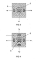
- Fig. 1 The two spatial areas with high magnetic permeability on the one hand and good insulation of the windings on the other hand are in basic form in Fig. 1 shown.
- a ring core 1 is shown, which is surrounded on the one hand by a primary winding 2 and on the other hand by a secondary winding 3.
- Fig. 2 Another basic design is in Fig. 2 shown.
- two ring cores 1a and 1b are provided, which are arranged side by side in the horizontal direction, wherein both ring cores 1a and 1b are surrounded by a primary winding 2 and a secondary winding 3, which are arranged horizontally one above the other.
- Fig. 3 is a sectional view in the plane of the primary winding 2 as shown Fig. 2 shown.
- the winding 2 can be seen, which surrounds a central region 11 of the ferrite core, which is formed by the ring cores 1a and 1b.
- a ferrite core of the inductive component is formed.
- the vertical ferrite legs detected in the sectional view are closed by ferrite covering layers on the top and bottom sides of these ring cores 1a and 1b.
- the windings 2 and 3 and the ring cores 1a and 1b are embedded in a dielectric 4.
- Fig. 4 is a further sectional view shown, which shows an approximation to a pot core with five vertical legs of ferrite material.
- the Legs are characterized by the central region 11 and the vertical outer legs 1a, 1b, 1c and 1d. Again, the arrangement is embedded in an insulating dielectric medium.
- a method of fabricating a monolithic integrated planar transformer based on LTCC technology is known.
- the in the Fig. 1 and 2 The basic structures shown are made by combining a low-permeability material at higher resistivity and a higher-permeability material at lower resistivity.
- the integration of these two materials is carried out by punching out openings in the films of the one material, filling the openings with pieces of film or film stacks of the other material and then sintering together.
- This intarsia process is complex and error-prone even with well-matched materials and thus relatively expensive, since the films must be processed on impact.
- WO 2005/032226 shows the features of the preamble of claim 1.
- the present invention is therefore based on the object to provide a method with which an inductive component with high dielectric strength can be produced with little effort. In addition, it is also an object to provide such an inductive component.
- this is formed from a plurality of layers.
- an electrically conductive material is arranged as a winding or winding of the component on a first non-magnetic, dielectric ceramic layer.
- at least one continuous recess is formed in the non-magnetic dielectric ceramic layer.
- a first magnetic ceramic layer or a corresponding layer stack is disposed on an upper surface of this non-magnetic dielectric ceramic layer.
- a separate second magnetic ceramic layer or a corresponding one Layer stack is placed on a bottom surface of the non-magnetic dielectric ceramic layer.
- This thus created intermediate state of the inductive component is then subjected to at least one further process step, in which at least one of the magnetic ceramic layers is plastically deformed, such that the two magnetic ceramic layers are contacted in the region of the recess and form a magnetic core of the device.
- an inductive component can be produced in a low-cost and thus also cost-effective manner.
- the inductive component can be generated with an optimized dielectric strength between the windings or the windings of the inductive component.
- the order of the process steps is not specified by the list above. In particular, the first two steps can also be performed in reverse order.
- the electrically conductive material is embedded or printed in the non-magnetic dielectric ceramic layer.
- the non-magnetic dielectric ceramic layer and the magnetic ceramic layers are preferably provided as foils.
- the dimensions of the recess in the plane of the ceramic layer are made larger in comparison with the thickness of the ceramic layer.
- the windings or windings are thus preferably embedded conventionally in the non-magnetic dielectric ceramic layer or at least printed there.
- lay numbers from 5 to 10 are sufficient for a variety of applications and thus results in a relatively low material thickness of the entire inductive component of a few 100 microns.
- at least one non-magnetic, dielectric ceramic layer is provided with preferably punched openings whose extent is large in comparison to the material thickness of the multilayer.
- a recess has a diameter between 1 mm and 3 mm, preferably about 2 mm.
- At least one closed covering film of ferrite is then advantageously laminated to the upper side and the underside of this non-magnetic, dielectric ceramic layer in an advantageous manner.
- the windings are covered by another non-magnetic dielectric ceramic layer and thus are substantially completely surrounded by nonmagnetic dielectric material.
- a direct connection with the magnetic ceramic layers is not provided in this embodiment.
- the process step for plastically deforming at least one magnetic ceramic layer as a sintering process is advantageously carried out.
- This sintering process is performed so that the magnetic ceramic layers, which are preferably ferrite foils, are centered on each other by plastic deformation due to the softening of the glass portion in the recess of the non-magnetic dielectric ceramic material.
- a support can be applied, which is arranged to support the deformation of this ceramic layer.
- the deformation can be carried out in a location-specific manner, and the deformation of the magnetic ceramic layers into the recess and thus also the contacting of the two magnetic ceramic layers can be improved.
- the contact surface between the two magnetic ceramic layers can thereby be made as large as possible.
- a plurality of non-magnetic, dielectric layers are stacked, wherein at least one recess is formed in each of the non-magnetic, dielectric ceramic layers and the non-magnetic, dielectric ceramic layers are arranged one above the other such that these recesses overlap at least in regions.
- a recess is formed in a non-magnetic, dielectric ceramic layer of different dimensions to a recess of at least a second non-magnetic, dielectric ceramic layer.
- the non-magnetic dielectric ceramic layers are then preferably stacked such that one through all non-magnetic, dielectric ceramic layers continuous recess is formed at least partially tapered.
- a recess is formed, which is initially formed to be tapered and then widens again.
- this taper and subsequent expansion in a cross-sectional view is formed such that the continuous recess is formed symmetrically to a horizontal symmetry line in a cross-sectional view.
- the taper is formed as a stepped profile.
- Stepped magnetic vias offer a high degree of design freedom in terms of the number of dielectric and magnetic layers.
- a magnetic material is applied, wherein the magnetic ceramic layer is arranged on the non-magnetic, dielectric ceramic layer, that the magnetic material is positioned in the region of the recess.
- the magnetic material is preferably applied with such a structure that substantially corresponds to the inverse configuration of the tapered recess of the plurality of stacked non-magnetic dielectric ceramic layers. With more turns and higher number of layers, such a step design in the region of this recess avoids too small radii of curvature of the outer magnetic ceramic layers, in particular of the ferrite layers.
- this magnetic material is printed on the magnetic ceramic layers.
- a reduction of the plastic deformation of the magnetic ceramic layers in the region of the recess can thereby be achieved.
- this magnetic material is printed as a thick-film ferritic paste by a screen printing process.
- ferrite paste can be repeatedly printed on the magnetic ceramic layers in the region of the recess before laminating in order to close the recess completely and thus to be able to form without an air gap.
- At least two non-magnetic, dielectric ceramic layers are formed, between which a magnetic layer, in particular a magnetic ceramic layer, is formed.
- this magnetic ceramic layer is formed as a continuous layer. This allows you to set specific field lines. For example, field lines can escape laterally without penetrating all turns. The size of this leakage inductance can be adjusted specifically by the thickness of this additionally introduced magnetic ceramic layer.
- the electrically conductive material for forming turns may be formed on an upper side and a lower side of this nonmagnetic dielectric ceramic layer.
- the electrically conductive material may be arranged to form a primary winding and a secondary winding of the inductive component.
- the non-magnetic, dielectric ceramic layer is preferably formed with a thickness between 20 ⁇ m and 200 ⁇ m, in particular between 50 ⁇ m and 100 ⁇ m.
- the conductor tracks or windings can be completely embedded in highly insulating, dielectric ceramic. Due to the high dielectric strength, these ceramic layers can be made correspondingly thinner, whereby costs can be saved and the size can be minimized.
- the inductive component is preferably designed as a monolithically integrated planar transformer.
- the functions of magnetic permeability and electrical insulation are realized in their respective space regions by tailoring specific ceramics, respectively, resulting in high efficiency of the design and the requirement and application of the component.
- different ceramics can be used.
- hexa-ferrite ceramics in particular barium-hexa-ferrite ceramics, can preferably be used. These have a permeability between about 10 and 30.
- a second class of ceramics may be used when frequencies in the middle range of about 10 to about 30 MHz are required.
- CuNiZn ferrite materials can be used.
- the permeability Ceramics used for components for use in this medium frequency range have permeability values of about 150 to about 500.
- ceramics used in this class have permeability values between about 500 and 1000.
- An inductive component according to the invention is constructed from a plurality of layers, and in particular realized as a monolithically integrated planar transformer.
- the inductive component comprises at least one electrically conductive winding which is arranged on a first non-magnetic, dielectric ceramic layer. At least one continuous recess is formed in this at least one non-magnetic, dielectric ceramic layer.
- the inductor further includes a first magnetic ceramic layer disposed on an upper surface of the non-magnetic dielectric ceramic layer.
- a second magnetic ceramic layer is on a bottom side arranged this non-magnetic dielectric ceramic layer.
- At least one of these two magnetic ceramic layers is plastically deformed in the region of the recess in such a way that it is connected to the other magnetic ceramic layer in the region of the recess and, overall, a magnetic core of the component is formed by these two ceramic layers.
- the inductive component provided in this way has an optimized dielectric strength between the windings or windings and, moreover, can be produced inexpensively.
- non-magnetic material herein is meant a material having a relative magnetic permeability close to or equal to 1 as compared to the magnetic material used for the magnetic ceramic layer.
- FIG. 5 an example of a completed monolithically integrated planar transformer I is shown, which forms the starting point of the illustrated invention. It is a longitudinal section through a Layer stack shown, with only the essential part of the planar transformer I is shown for the invention.
- the sectional view shows a planar transformer I with a low number of turns, which was produced in LTCC technology.
- the planar transformer I has a non-magnetic, dielectric ceramic layer 5, which is formed as a foil.
- On the upper side 51 of this dielectric ceramic layer 5 self-contained conductive traces or windings 511, 512, 513 and 514 are arranged in the exemplary embodiment, which surround the transformer core in a specific sense of rotation and constitute turns of a primary winding of the planar transformer 1.
- this primary winding is spiral-shaped. At non-illustrated ends of this winding contacts are provided, through which an electrical connection with a power supply can be made possible.
- a secondary winding is formed, which comprises the windings 521, 522, 523 and 524.
- This secondary winding also has ends which are provided for further electrical contacting.
- Both the turns 511 to 514 of the primary winding and the turns 521 to 524 of the secondary winding are printed in a conventional manner on the upper side 51 and on the lower side 52 of the dielectric ceramic layer 5, respectively.
- planar transformer I has a continuous recess 53, which is produced by a stamping process.
- a first magnetic ceramic layer 6 is arranged on the upper side 51 and directly on the windings 511 to 514.
- a second magnetic ceramic layer 7 is disposed on the underside 52 and directly on the windings 521 to 524 of the secondary winding.
- these two separate magnetic ceramic layers 6 and 7 are plastically deformed and connected to each other in the middle.
- a magnetic via is formed in the region of the recess 53, as a result of which the two magnetic ceramic layers 6 and 7 form a magnetic core of the planar transformer I.
- the magnetic ceramic layers 6 and 7 are also contacted with one another at the edge regions facing away from the recess 53 in the x-direction.
- This contacting at the edge regions is also formed by a plastic deformation of at least one of the ceramic layers 6 or 7.
- the indentations in the y-direction in the region of the recess 53 resulting from the plastic deformation of the ceramic layers 6 and 7 can be planarized as required by a subsequent doctoring process.
- a further dielectric paste can be applied at the appropriate points, which is formed flat by this doctor blade process.
- the in Fig. 5 shown finished planar transformer I is formed such that first the dielectric ceramic layer 5 is prepared and prepared for further processing. For this purpose, the at least one recess 53 is punched out. Further, then, the electrically conductive material for forming the windings 511 to 514 and the windings 521 to 524 printed on the corresponding surfaces of this dielectric ceramic layer 5.
- the recess in the x-direction and also in the z-direction (perpendicular to the plane of the figure) is punched out with dimensions which are substantially greater than the thickness (y-direction) of the dielectric ceramic layer 5.
- a central region 9 of the magnetic core of the planar transformer I is formed.
- the sintering process takes place.
- the plastic deformation thus takes place through the lamination process.
- a stack of a plurality of magnetic layers may be formed in each case corresponding to the requirements of the component.
- FIG. 6 An embodiment of a monolithically integrated planar transformer II, which was produced in LTCC technology is in Fig. 6 shown. Again, a longitudinal sectional view of a partial section of a completed planar transformer II shown. The sectional view shows a structure of the planar transformer II, which has a high number of turns.
- the planar transformer II has non-magnetic dielectric ceramic layers 5a, 5b, 5c, 5d and 5e stacked one above the other. On the dielectric ceramic layers 5a, 5b, 5d and 5e windings are respectively applied to the upper sides.
- the turns 511b, 512b, 513b and 514b are mentioned, which are printed on an upper side 51b of the dielectric ceramic layer 5b.
- the windings 511a, 512a, 513a and 514a are printed on an upper side 51a of the dielectric ceramic layer 5a. These windings are assigned in the embodiment of a primary winding of the planar transformer II.
- the unspecified, printed on the dielectric ceramic layers 5d and 5e turns are associated with a secondary winding of the planar transformer II.
- the windings can also be arranged such that turns arranged on an upper side, for example on the top side of the dielectric ceramic layer 5a, are alternately assigned one of the primary winding and the subsequent secondary winding in the x direction.
- the dielectric ceramic layer 5c is arranged as a final covering layer.
- the turns of the planar transformer II are thereby completely surrounded by dielectric ceramic material.
- magnetic ceramic layers 6 and 7 are laminated on the opposite sides of the stacked dielectric ceramic layer 5a to 5e, which are plastically deformed in the region of a recess 53 ', so that they are interconnected in this area. As a result, a central region 9 'of the magnetic core of the planar transformer II is also formed here.
- the stacked dielectric ceramic layers 5a to 5e each have recesses having different dimensions.
- the dielectric ceramic layers 5a to 5e are stacked in such a way that the individual recesses formed in each of these ceramic layers form a common continuous recess 53 '.
- the dielectric ceramic layer 5c in the sectional view shown has a recess which, at least in the x-direction, is larger than the recesses formed individually in the electrical ceramic layers 5b, 5a and 5d.
- the recesses formed in the dielectric ceramic layers 5b and 5d are larger than the recess formed in the dielectric ceramic layer 5a.
- the dielectric ceramic layers 5a to 5e are stacked on top of each other in such a way that a tapering recess 53 'results in the y direction from the upper dielectric ceramic layer 5c to the centrally arranged dielectric ceramic layer 5a.
- a stepped profile is realized. Starting from the central dielectric ceramic layer 5a, this recess 53 'widens in the y-direction up to the lower dielectric ceramic layer 5e again. Also, a step profile is formed.
- the planar transformer II is formed symmetrically with respect to an axis of symmetry drawn through the dielectric ceramic layer 5a in the x direction.
- planar transformer II shown in the completed state is preferably analogous to the preparation of the in Fig. 5 shown planar transformer I performed.
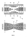
- Fig. 7 is a further longitudinal section through a planar transformer III shown, which is shown in a not yet completed process stage. Again, only a partial section is shown, which shows the essential structure in a central region of the device.
- the configuration and arrangement of the non-magnetic, dielectric ceramic layers 5a to 5e is analogous to the embodiment according to FIG Fig. 6 ,
- the first magnetic ceramic layer 6 or possibly a corresponding layer stack is provided with an additional structure comprising the layers 6a and 6b.
- These layers 6a and 6b are made of a magnetic material, and are applied in the embodiment of ferritic thick-film paste by means of screen printing. It can be seen that these layers 6a and 6b are formed on the surface of the magnetic ceramic layer 6 facing the dielectric ceramic layers 5a to 5e.
- These layers 6a and 6b are formed as a stepped profile and designed so that they are designed as a complementary structure to the step configuration of the dielectric ceramic layers 5c and 5b.
- layers 7a and 7b are also arranged on the second magnetic ceramic layer 7 or, if appropriate, a corresponding layer stack, which are designed as a stepped profile and as a complementary structure with respect to the step profile which is produced by the dielectric ceramic layers 5d and 5e .
- the magnetic ceramic layers 6 and 7 are positioned in a subsequent process such that, as in FIG Fig. 7 4, the layers 6a and 6b and the layers 7a and 7b are disposed substantially in the region of the step profile formed by the dielectric ceramic layers 5a to 5b.
- these structures of the ceramic layers 6 and 7 are laminated onto the stacked form of the dielectric ceramic layers 5a to 5e to form a recess 53 " of planar transformer III.
- FIG. 8 is a further longitudinal sectional view of another Ausfaturigsbeispiels of a monolithically integrated planar transformer IV shown.
- the planar transformer IV is shown in a completed state. It can be seen that between an dielectric ceramic layer 5a and a dielectric ceramic layer 5f an intermediate layer is formed, which is formed as a further magnetic ceramic layer 10. In a symmetrical arrangement are to this Magnetic ceramic layer 10 each stacked and in the region of a recess 53 '''stepped designed dielectric ceramic layers 5a, 5b and 5c and 5f, 5g and 5h arranged.
- a central region 9 "of the magnetic core of the planar transformer IV is formed, and by integrating a central magnetic ceramic layer 10, which may be a ferrite foil, field lines of the primary winding (in the exemplary embodiment, the turns arranged on the ceramic layers 5g, 5h) are present.
Landscapes
- Engineering & Computer Science (AREA)
- Power Engineering (AREA)
- Manufacturing & Machinery (AREA)
- Microelectronics & Electronic Packaging (AREA)
- Coils Or Transformers For Communication (AREA)
- Manufacturing Cores, Coils, And Magnets (AREA)
Abstract
Claims (8)
- Procédé de fabrication d'un composant inductif, qui est constitué de plusieurs couches, dans lequel on effectue les stades suivants :a) on met un matériau ( 511 à 514 ; 521 à 524 ), conducteur de l'électricité, comme enroulement du composant ( I, II, III, VI ) sur une première couche ( 5; 5a à 5h ) en céramique diélectrique amagnétique ;b) on forme au moins un évidement ( 53, 53', 53", 53"') traversant dans la couche ( 5, 5a à 5h ) diélectrique amagnétique ;c) on met une première couche ( 6 ) en céramique magnétique sur une face supérieure et une deuxième couche ( 7 ) en céramique magnétique sur une face inférieure de la couche ( 5, 5a à 5h ) en céramique diélectrique amagnétique ; etd) on effectue un stade opératoire, dans lequel on déforme plastiquement au moins l'une des couches ( 6, 7 ) en céramique magnétiques, de manière à ce que les deux couches ( 6, 7 ) en céramique magnétiques soient en contact dans la zone de l'évidement ( 53, 53', 53", 53''') et forment un noyau magnétique du composant ( I, II, III, VI ),dans lequel le procédé est caractérisé en ce que on dépose sur le matériau ( 511 à 514 ; 521 à 524 ), conducteur de l'électricité, une autre couche diélectrique amagnétique, notamment une couche ( 5c, 5f ) en céramique, dans lequel on empile une multiplicité de couches ( 5a à 5h ) en céramique diélectriques amagnétiques, dans lesquelles on forme respectivement au moins un évidement, les couches ( 5a à 5h ) en céramique diélectriques amagnétiques étant superposées, de manière à ce que les évidements se chevauchent, au moins par endroit,
et dans lequel on forme et on empile les évidements des couches ( 5a à 5h ) en céramique respectives, de dimension différente, de façon à former un évidement (53', 53", 53''') traversant toutes les couches ( 5a à 5h ) en céramique diélectriques amagnétiques et se rétrécissant au moins par endroit. - Procédé suivant la revendication 1,
caractérisé en ce que
on met au moins sur une couche ( 6, 7 ) en céramique magnétique, pendant le stade d ), un appui pour favoriser la déformation de cette couche ( 6, 7 ) en céramique. - Procédé suivant l'une des revendications précédentes,
caractérisé en ce que
on dépose un matériau ( 6a, 6b ; 7a, 7b ) magnétique, au moins sur une couche ( 6, 7 ) en céramique magnétique, la couche ( 6, 7 ) en céramique magnétique étant disposée suivant le stade c) sur la couche ( 5, 5a à 5h ) en céramique diélectrique amagnétique, de manière à mettre le matériau ( 6a, 6 ; 7a, 7b ) magnétique en position dans la zone de l'évidement ( 53, 53', 53', 53'''). - Procédé suivant l'une des revendications précédentes,
caractérisé en ce que
on forme au moins deux couches ( 5a à 5h ) en céramique diélectriques amagnétiques entre lesquelles on forme une couche magnétique, notamment une couche ( 10 ) en céramique. - Procédé suivant l'une des revendications précédentes,
caractérisé en ce que
on forme les couches ( 5, 5a à 5h ) en céramique diélectrique amagnétique en une épaisseur comprise entre 20µm et 200µm, notamment entre 50µm et 100µm. - Composant inductif, qui comporte une multiplicité de couches et dans lequel- au moins un enroulement conducteur de l'électricité du composant ( I, II, III, VI ) est disposé sur une première couche ( 5, 5a à 5h ) en céramique diélectrique amagnétique, dans laquelle est formée au moins un évidement ( 53, 53', 53", 53"') traversant ;- et une première couche ( 6 ) en céramique magnétique est disposée sur une face supérieure et une deuxième couche ( 16 ) en céramique magnétique sur une face inférieure de la couche ( 5, 5a à 5h ) en céramique diélectrique amagnétique, au moins une couche ( 6, 7 ) en céramique magnétique étant déformée plastiquement dans la zone de l'évidement ( 53, 53', 53" , 53" ), de manière à être reliée à l'autre couche ( 6, 7 ) en céramique magnétique et à former un noyau magnétique du composant ( I, II, III, VI ),dans lequel l'élément inductif est caractérisé en ce que une multiplicité de couches ( 5a à 5h ) en céramique diélectriques amagnétiques est empilée, couches dans lesquelles respectivement au moins un évidement est formé, les couches ( 5a à 5h ) en céramique diélectriques amagnétiques étant superposées, de manière à ce que les évidements se chevauchent au moins par endroit,
et dans lequel les évidements des couches ( 5a à 5h ) en céramique respectives ont des dimensions différentes et les couches ( 5a à 5h ) en céramique sont empilées, de manière à former un évidement ( 53', 53", 53''') traversant toutes les couches ( 5a à 5h ) en céramique diélectriques amagnétiques, l'évidement se rétrécissant au moins par endroit. - Composant inductif suivant la revendication 6,
caractérisé en ce que
le rétrécissement a un profil en gradin. - Composant inductif suivant l'une des revendications 6 ou 7,
caractérisé en ce qu'au moins deux couches ( 5a à 5h ) en céramique diélectriques amagnétiques sont formées, couches entre lesquelles est formée une couche magnétique, notamment une couche ( 10 ) en céramique.
Applications Claiming Priority (2)
| Application Number | Priority Date | Filing Date | Title |
|---|---|---|---|
| DE102006022785A DE102006022785A1 (de) | 2006-05-16 | 2006-05-16 | Induktives Bauelement und Verfahren zum Herstellen eines induktiven Bau-elements |
| PCT/EP2007/054285 WO2007131884A1 (fr) | 2006-05-16 | 2007-05-03 | composant inductif et procédé de réalisation d'un composant inductif |
Publications (2)
| Publication Number | Publication Date |
|---|---|
| EP2018643A1 EP2018643A1 (fr) | 2009-01-28 |
| EP2018643B1 true EP2018643B1 (fr) | 2010-11-24 |
Family
ID=38330479
Family Applications (1)
| Application Number | Title | Priority Date | Filing Date |
|---|---|---|---|
| EP07728738A Not-in-force EP2018643B1 (fr) | 2006-05-16 | 2007-05-03 | Composant inductif et procede de realisation d'un composant inductif |
Country Status (8)
| Country | Link |
|---|---|
| US (1) | US7973631B2 (fr) |
| EP (1) | EP2018643B1 (fr) |
| JP (1) | JP4971432B2 (fr) |
| KR (1) | KR101433838B1 (fr) |
| CN (1) | CN101443863B (fr) |
| DE (2) | DE102006022785A1 (fr) |
| TW (1) | TW200802436A (fr) |
| WO (1) | WO2007131884A1 (fr) |
Families Citing this family (16)
| Publication number | Priority date | Publication date | Assignee | Title |
|---|---|---|---|---|
| DE102006025098B4 (de) * | 2006-05-19 | 2008-06-05 | Fraunhofer-Gesellschaft zur Förderung der angewandten Forschung e.V. | Sensor zur Ermittlung der elektrischen Leitfähigkeit flüssiger Medien und ein Verfahren zu seiner Herstellung |
| WO2009125656A1 (fr) * | 2008-04-08 | 2009-10-15 | 株式会社村田製作所 | Composant électronique |
| CN102637677A (zh) * | 2012-04-24 | 2012-08-15 | 上海宏力半导体制造有限公司 | 电感及其形成方法、射频器件、集成无源器件 |
| WO2013183452A1 (fr) * | 2012-06-08 | 2013-12-12 | 株式会社村田製作所 | Composant électronique et procédé de fabrication de celui-ci |
| JP6090902B2 (ja) * | 2012-10-17 | 2017-03-08 | Necトーキン株式会社 | コイル部品 |
| WO2015069279A1 (fr) * | 2013-11-08 | 2015-05-14 | Empire Technology Development Llc | Appareil et procédés pour détecter l'alignement d'un substrat durant un processus d'impression |
| JP5999119B2 (ja) * | 2014-02-10 | 2016-09-28 | 株式会社村田製作所 | インダクタ |
| KR101762778B1 (ko) | 2014-03-04 | 2017-07-28 | 엘지이노텍 주식회사 | 무선 충전 및 통신 기판 그리고 무선 충전 및 통신 장치 |
| DE102014218638A1 (de) * | 2014-09-17 | 2016-03-31 | Siemens Aktiengesellschaft | Herstellen eines Bauteils mit einem Keramikpulverkörper |
| KR20160117943A (ko) * | 2015-04-01 | 2016-10-11 | 삼성전기주식회사 | 코일 부품 |
| DE102015206697A1 (de) * | 2015-04-15 | 2016-10-20 | Schaeffler Technologies AG & Co. KG | Primärteil einer elektrischen Maschine, elektrische Maschine und Verfahren zur Herstellung eines Primärteils |
| DE102018204366A1 (de) * | 2018-03-22 | 2019-09-26 | Robert Bosch Gmbh | Induktives Bauelement und Hochfrequenz-Filtervorrichtung |
| KR102019877B1 (ko) | 2019-05-08 | 2019-11-04 | 국방과학연구소 | 코일형 전도성 미세 입자를 이용한 유효 투자율을 가지는 입자-매질 복합소재 |
| US11387678B2 (en) | 2019-09-27 | 2022-07-12 | Apple Inc. | Stacked resonant structures for wireless power systems |
| US20210098180A1 (en) * | 2019-09-30 | 2021-04-01 | Advanced Semiconductor Engineering, Inc. | Inductor structure |
| CN113593858A (zh) * | 2021-08-13 | 2021-11-02 | 上海东归电子系统科技有限公司 | 一种基于金属化陶瓷的感应加热变压器绕组结构 |
Family Cites Families (18)
| Publication number | Priority date | Publication date | Assignee | Title |
|---|---|---|---|---|
| KR890004585B1 (ko) * | 1980-09-11 | 1989-11-16 | 아사히가세이고교가부시키가이샤 | 마이크로코일(microcoil) |
| US5349743A (en) * | 1991-05-02 | 1994-09-27 | At&T Bell Laboratories | Method of making a multilayer monolithic magnet component |
| WO1996042095A1 (fr) * | 1995-06-13 | 1996-12-27 | Nihon Shingo Kabushiki Kaisha | Transformateur plat |
| JPH09199331A (ja) * | 1996-01-18 | 1997-07-31 | Matsushita Electric Ind Co Ltd | コイル部品およびその製造方法 |
| JPH10189342A (ja) * | 1996-12-24 | 1998-07-21 | Matsushita Electric Ind Co Ltd | コモンモードチョークコイルおよびその製造方法 |
| US6198374B1 (en) * | 1999-04-01 | 2001-03-06 | Midcom, Inc. | Multi-layer transformer apparatus and method |
| JP2001007468A (ja) * | 1999-06-24 | 2001-01-12 | Nec Kansai Ltd | 配線基板,多層配線基板およびその製造方法 |
| DE60137613D1 (de) * | 2000-06-20 | 2009-03-26 | Murata Manufacturing Co | Spulenvorrichtung und Verfahren zu ihrer Herstellung |
| DE10030605A1 (de) * | 2000-06-21 | 2002-01-03 | Philips Corp Intellectual Pty | Elektronisches Bauteil |
| ITTO20001128A1 (it) * | 2000-12-04 | 2002-06-04 | Fiat Ricerche | Induttore planare con nucleo ferromagnetico e relativo metodo di fabbricazione. |
| JP4092914B2 (ja) * | 2001-01-26 | 2008-05-28 | セイコーエプソン株式会社 | マスクの製造方法、有機エレクトロルミネッセンス装置の製造方法 |
| US6611046B2 (en) * | 2001-06-05 | 2003-08-26 | 3M Innovative Properties Company | Flexible polyimide circuits having predetermined via angles |
| JP2002373810A (ja) * | 2001-06-14 | 2002-12-26 | Tdk Corp | チップ型コモンモードチョークコイル |
| KR100466884B1 (ko) * | 2002-10-01 | 2005-01-24 | 주식회사 쎄라텍 | 적층형 코일 부품 및 그 제조방법 |
| CN100587560C (zh) * | 2003-04-01 | 2010-02-03 | 夏普株式会社 | 发光装置用组件、发光装置、背侧光照射装置、显示装置 |
| AU2003266683A1 (en) * | 2003-09-29 | 2005-04-14 | Tamura Corporation | Multilayer laminated circuit board |
| JP2005268455A (ja) * | 2004-03-17 | 2005-09-29 | Murata Mfg Co Ltd | 積層型電子部品 |
| JP2007081613A (ja) * | 2005-09-13 | 2007-03-29 | Seiko Epson Corp | 弾性表面波デバイス及びその製造方法 |
-
2006
- 2006-05-16 DE DE102006022785A patent/DE102006022785A1/de not_active Withdrawn
-
2007
- 2007-05-03 WO PCT/EP2007/054285 patent/WO2007131884A1/fr not_active Ceased
- 2007-05-03 CN CN2007800177067A patent/CN101443863B/zh not_active Expired - Fee Related
- 2007-05-03 US US12/300,909 patent/US7973631B2/en not_active Expired - Fee Related
- 2007-05-03 JP JP2009510399A patent/JP4971432B2/ja not_active Expired - Fee Related
- 2007-05-03 DE DE502007005763T patent/DE502007005763D1/de active Active
- 2007-05-03 KR KR1020087030628A patent/KR101433838B1/ko not_active Expired - Fee Related
- 2007-05-03 EP EP07728738A patent/EP2018643B1/fr not_active Not-in-force
- 2007-05-09 TW TW096116383A patent/TW200802436A/zh unknown
Also Published As
| Publication number | Publication date |
|---|---|
| JP2009537976A (ja) | 2009-10-29 |
| EP2018643A1 (fr) | 2009-01-28 |
| JP4971432B2 (ja) | 2012-07-11 |
| CN101443863B (zh) | 2012-05-30 |
| TW200802436A (en) | 2008-01-01 |
| US7973631B2 (en) | 2011-07-05 |
| WO2007131884A1 (fr) | 2007-11-22 |
| DE102006022785A1 (de) | 2007-11-22 |
| DE502007005763D1 (de) | 2011-01-05 |
| US20090102591A1 (en) | 2009-04-23 |
| CN101443863A (zh) | 2009-05-27 |
| KR101433838B1 (ko) | 2014-08-27 |
| KR20090015975A (ko) | 2009-02-12 |
Similar Documents
| Publication | Publication Date | Title |
|---|---|---|
| EP2018643B1 (fr) | Composant inductif et procede de realisation d'un composant inductif | |
| DE69519476T2 (de) | Herstellungsverfahren für einen Magnetkreis in einem integrierten Kreis | |
| JP3621300B2 (ja) | 電源回路用積層インダクタ | |
| KR100552010B1 (ko) | 적층전자부품 및 그 제조방법 | |
| DE19723068C1 (de) | Induktives Bauelement | |
| DE3145585C2 (fr) | ||
| EP2158597B1 (fr) | Composant inductif monolithique, procédé de fabrication du composant et utilisation du composant | |
| EP3547338A1 (fr) | Composant électronique et son procédé de fabrication | |
| DE102018113765B4 (de) | Transformator mit einer durchkontaktierung für einen magnetkern | |
| DE10002377A1 (de) | Spule und Spulensystem zur Integration in eine mikroelektronische Schaltung sowie mikroelektronische Schaltung | |
| DE68908234T2 (de) | Integrierter Kondensator und Spulen/Transformatoren mit isoliertem, amorphem Metallband. | |
| DE69007703T2 (de) | Induktoren des Typs aus gestapelten Schichten zusammengesetzter Wirkung, einschliesslich Induktoren mit Induktivität und Gegeninduktivität und ihr Herstellungsverfahren. | |
| WO2020025500A1 (fr) | Procédé de fabrication d'un composant inductif et composant inductif | |
| WO2015176919A1 (fr) | Composant passif inductif multicouches et corps de film permettant la production de ce dernier | |
| DE69623867T2 (de) | Chip-Antenne | |
| DE102016223195A1 (de) | Transformatorvorrichtung, Transformator und Verfahren zur Herstellung einer Transformatorvorrichtung | |
| DE102008049756A1 (de) | Schaltungsträger mit Transformator | |
| DE202019102273U1 (de) | Induktives Bauelement | |
| DE102014114205A1 (de) | Planarer Miniaturtransformator | |
| DE4312455A1 (de) | Nicht-reziprokes Schaltungselement | |
| DE112017004276T5 (de) | Verfahren zur herstellung einer induktiven komponente und eine induktive komponente | |
| DE3628021A1 (de) | Chip-bauteil mit wenigstens einer spule und verfahren zu dessen herstellung | |
| DE10338471A1 (de) | Miniaturisierte, magnetische Bauelemente und Verfahren zu ihrer Herstellung mit Hilfe von Wafer-Level-Technologie | |
| DE102013205655A1 (de) | Mehrlagiges induktives passives Bauelement und Folienkörper zu dessen Herstellung | |
| DE102023101144A1 (de) | Filter zur Unterdrückung von Gleichtaktstörungen und/oder Gegentaktstörungen |
Legal Events
| Date | Code | Title | Description |
|---|---|---|---|
| PUAI | Public reference made under article 153(3) epc to a published international application that has entered the european phase |
Free format text: ORIGINAL CODE: 0009012 |
|
| 17P | Request for examination filed |
Effective date: 20080925 |
|
| AK | Designated contracting states |
Kind code of ref document: A1 Designated state(s): AT BE BG CH CY CZ DE DK EE ES FI FR GB GR HU IE IS IT LI LT LU LV MC MT NL PL PT RO SE SI SK TR |
|
| AX | Request for extension of the european patent |
Extension state: AL BA HR MK RS |
|
| DAX | Request for extension of the european patent (deleted) | ||
| RBV | Designated contracting states (corrected) |
Designated state(s): DE FR GB HU IT |
|
| 17Q | First examination report despatched |
Effective date: 20090529 |
|
| GRAP | Despatch of communication of intention to grant a patent |
Free format text: ORIGINAL CODE: EPIDOSNIGR1 |
|
| GRAS | Grant fee paid |
Free format text: ORIGINAL CODE: EPIDOSNIGR3 |
|
| GRAA | (expected) grant |
Free format text: ORIGINAL CODE: 0009210 |
|
| AK | Designated contracting states |
Kind code of ref document: B1 Designated state(s): DE FR GB HU IT |
|
| REG | Reference to a national code |
Ref country code: GB Ref legal event code: FG4D Free format text: NOT ENGLISH |
|
| REF | Corresponds to: |
Ref document number: 502007005763 Country of ref document: DE Date of ref document: 20110105 Kind code of ref document: P |
|
| PLBE | No opposition filed within time limit |
Free format text: ORIGINAL CODE: 0009261 |
|
| STAA | Information on the status of an ep patent application or granted ep patent |
Free format text: STATUS: NO OPPOSITION FILED WITHIN TIME LIMIT |
|
| 26N | No opposition filed |
Effective date: 20110825 |
|
| REG | Reference to a national code |
Ref country code: DE Ref legal event code: R097 Ref document number: 502007005763 Country of ref document: DE Effective date: 20110825 |
|
| PG25 | Lapsed in a contracting state [announced via postgrant information from national office to epo] |
Ref country code: IT Free format text: LAPSE BECAUSE OF FAILURE TO SUBMIT A TRANSLATION OF THE DESCRIPTION OR TO PAY THE FEE WITHIN THE PRESCRIBED TIME-LIMIT Effective date: 20101124 |
|
| REG | Reference to a national code |
Ref country code: DE Ref legal event code: R081 Ref document number: 502007005763 Country of ref document: DE Owner name: SIEMENS AKTIENGESELLSCHAFT, DE Free format text: FORMER OWNER: OSRAM GESELLSCHAFT MIT BESCHRAENKTER HAFTUNG, 81543 MUENCHEN, DE Effective date: 20111214 |
|
| REG | Reference to a national code |
Ref country code: DE Ref legal event code: R081 Ref document number: 502007005763 Country of ref document: DE Owner name: SIEMENS AKTIENGESELLSCHAFT, DE Free format text: FORMER OWNER: OSRAM AG, 81543 MUENCHEN, DE Effective date: 20121126 |
|
| PG25 | Lapsed in a contracting state [announced via postgrant information from national office to epo] |
Ref country code: HU Free format text: LAPSE BECAUSE OF FAILURE TO SUBMIT A TRANSLATION OF THE DESCRIPTION OR TO PAY THE FEE WITHIN THE PRESCRIBED TIME-LIMIT Effective date: 20101124 |
|
| REG | Reference to a national code |
Ref country code: FR Ref legal event code: PLFP Year of fee payment: 9 |
|
| PGFP | Annual fee paid to national office [announced via postgrant information from national office to epo] |
Ref country code: GB Payment date: 20150511 Year of fee payment: 9 |
|
| PGFP | Annual fee paid to national office [announced via postgrant information from national office to epo] |
Ref country code: FR Payment date: 20150513 Year of fee payment: 9 |
|
| PGFP | Annual fee paid to national office [announced via postgrant information from national office to epo] |
Ref country code: DE Payment date: 20150720 Year of fee payment: 9 |
|
| REG | Reference to a national code |
Ref country code: DE Ref legal event code: R119 Ref document number: 502007005763 Country of ref document: DE |
|
| GBPC | Gb: european patent ceased through non-payment of renewal fee |
Effective date: 20160503 |
|
| REG | Reference to a national code |
Ref country code: FR Ref legal event code: ST Effective date: 20170131 |
|
| PG25 | Lapsed in a contracting state [announced via postgrant information from national office to epo] |
Ref country code: FR Free format text: LAPSE BECAUSE OF NON-PAYMENT OF DUE FEES Effective date: 20160531 Ref country code: DE Free format text: LAPSE BECAUSE OF NON-PAYMENT OF DUE FEES Effective date: 20161201 |
|
| PG25 | Lapsed in a contracting state [announced via postgrant information from national office to epo] |
Ref country code: GB Free format text: LAPSE BECAUSE OF NON-PAYMENT OF DUE FEES Effective date: 20160503 |