EP2015556A2 - Mehrzweckgerät mit Scannermodul und Bildscanvorrichtung mit dem Scannermodul - Google Patents
Mehrzweckgerät mit Scannermodul und Bildscanvorrichtung mit dem Scannermodul Download PDFInfo
- Publication number
- EP2015556A2 EP2015556A2 EP08160134A EP08160134A EP2015556A2 EP 2015556 A2 EP2015556 A2 EP 2015556A2 EP 08160134 A EP08160134 A EP 08160134A EP 08160134 A EP08160134 A EP 08160134A EP 2015556 A2 EP2015556 A2 EP 2015556A2
- Authority
- EP
- European Patent Office
- Prior art keywords
- light
- scanner module
- document
- functional device
- module according
- Prior art date
- Legal status (The legal status is an assumption and is not a legal conclusion. Google has not performed a legal analysis and makes no representation as to the accuracy of the status listed.)
- Ceased
Links
Images












Classifications
-
- H—ELECTRICITY
- H04—ELECTRIC COMMUNICATION TECHNIQUE
- H04N—PICTORIAL COMMUNICATION, e.g. TELEVISION
- H04N1/00—Scanning, transmission or reproduction of documents or the like, e.g. facsimile transmission; Details thereof
- H04N1/024—Details of scanning heads ; Means for illuminating the original
- H04N1/028—Details of scanning heads ; Means for illuminating the original for picture information pick-up
- H04N1/02815—Means for illuminating the original, not specific to a particular type of pick-up head
-
- G—PHYSICS
- G02—OPTICS
- G02B—OPTICAL ELEMENTS, SYSTEMS OR APPARATUS
- G02B26/00—Optical devices or arrangements for the control of light using movable or deformable optical elements
- G02B26/08—Optical devices or arrangements for the control of light using movable or deformable optical elements for controlling the direction of light
- G02B26/10—Scanning systems
-
- G—PHYSICS
- G06—COMPUTING OR CALCULATING; COUNTING
- G06V—IMAGE OR VIDEO RECOGNITION OR UNDERSTANDING
- G06V10/00—Arrangements for image or video recognition or understanding
- G06V10/10—Image acquisition
-
- H—ELECTRICITY
- H04—ELECTRIC COMMUNICATION TECHNIQUE
- H04N—PICTORIAL COMMUNICATION, e.g. TELEVISION
- H04N1/00—Scanning, transmission or reproduction of documents or the like, e.g. facsimile transmission; Details thereof
- H04N1/024—Details of scanning heads ; Means for illuminating the original
- H04N1/028—Details of scanning heads ; Means for illuminating the original for picture information pick-up
- H04N1/02815—Means for illuminating the original, not specific to a particular type of pick-up head
- H04N1/0282—Using a single or a few point light sources, e.g. a laser diode
- H04N1/02835—Using a single or a few point light sources, e.g. a laser diode in combination with a light guide, e.g. optical fibre, glass plate
Definitions
- the present disclosure relates generally to a scanner module and an image scanning apparatus employing the same and, more particularly, to a scanner module that is capable of uniformly distributing illumination over a predetermined area of a document, and an image scanning apparatus employing the same.
- An image scanning apparatus generally includes a scanner module.
- a scanner module includes a number of components. These components include, for example, a sensing unit, an illuminator, a reflecting mirror, and an imaging lens. The scanning is performed by the illuminator first illuminating the document to be scanned.
- the light source in an illuminator is generally a lamp.
- the lamp in newer scanners may be either a cold cathode fluorescent lamp (CCFL) or a xenon lamp, while older scanners may have a standard fluorescent lamp. Specifically, the illuminator bounces the light from the illuminator off the reflecting mirror on to the document to be scanned.
- CCFL cold cathode fluorescent lamp
- the image of the document is reflected by an angled mirror or by a series of mirrors. In some scanners, there may only be two mirrors while others may use greater number of mirrors. Each mirror is slightly curved to focus the image it reflects onto a smaller surface. The last mirror reflects the image onto a lens. The lens focuses the image through a filter onto the sensing unit.
- a light source for a scanner module may beneficially have a number of features.
- the light source should provide sufficient brightness in an area on the paper where the image is to be read.
- the light source should allow for an uniform distribution of illumination over the document to ensure that the image is scanned properly.
- Various kinds of light sources have been developed to provide the light as part of the illuminator.
- a high intensity white light emitting diode (LED) has been developed as a light source to be used in a scanner module.
- the sensor unit used in the scanner module may be of different structures based on the type of image to be scanned. For example, a single-row structure may be used for scanning a black and white image but a plural row structure may be used for color image scanning.
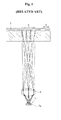
- FIG. 1 is a pictorial diagram illustrating a scanning module with a general color sensor unit for color image scanning.
- a sensor unit 7 includes color image sensors 7a provided in plural rows. These color image sensors 7a may be arranged according to the various colors being sensed. Furthermore, the rows of the color image sensor 7a are spaced apart from each other at a predetermined distance. An image from a predetermined scanning area A of a document 1 is focused on the sensor unit 7 by the imaging lens 5. For proper scanning, it may be beneficial that scanning area A on document 1 is illuminated uniformly.
- the focus position of a scanner module is the position where light is reflected from the document being scanned on to the sensor unit. Ideally, it would be most beneficial that the focus position of the scanning module be the same for all scanners. That is, the focus position be one as designated in the design specification of the scanner module. However, due to defects introduced during the manufacturing process of scanners, there may be deviations in the focus positions of the actual scanner modules.
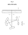
- FIGS. 2 and 3 are schematic views illustrating deviations in the focus position of the scanner module.
- the solid line indicates the light path of an ideally assembled scanner module where components thereof are properly positioned. That is, the solid line indicates the intended light path.
- the reflecting mirror 11 may be dislocated during the manufacture or during normal operation of the scanner module. Because of this dislocation, the focus position of the scanner module may deviate from the ideal position.
- a reflecting mirror 11 is dislocated as illustrated in FIG. 2 or if a sensor unit 25 is dislocated as illustrated in FIG. 3 , light may be incident via the abnormal light paths L 2 and L 4 instead of the ideal light paths L 1 and L 3 . Furthermore, this light that is incident via the abnormal light paths L 2 and L 4 is focused on the sensor units 15 and 25.
- the focusing position on the document 10 may be affected by operating conditions of the scanner module. For example, if the scanner module operates under high or low temperature environment characteristics, e.g., the position and/or the size of optical elements may be affected, resulting in a draft or deviation of the light path, which in turn may cause the focusing position on the document 1 to change.
- high or low temperature environment characteristics e.g., the position and/or the size of optical elements may be affected, resulting in a draft or deviation of the light path, which in turn may cause the focusing position on the document 1 to change.
- Various known techniques may be used to attempt to minimize the effect of the variation in the focusing position of the scanner module.
- the uniformity of illumination across the document 1 is maintained despite some deviation of the light path within a tolerable range.
- the conventional image scanner includes first and second LEDs 35a and 35b mounted on a substrate 31. LEDs 35a and 35b are spaced apart from each other in the X-direction. Furthermore, first and second condensing lenses 37a and 37b are provided integrally with the first and second LEDs 35a and 35b, respectively. First and second condensing lenses 37a and 37b are used to condense light.
- the first and second condensing lenses 37a and 37b are arranged to make light emitted from the first and second LEDs 35a and 35b travel in a direction not parallel to the direction normal to the substrate 31. Furthermore, as shown in FIG. 4 , the first and second condensing lenses 37a and 37b illuminate a predetermined position C of a document mount 39 on which the document is to be mounted.
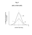
- FIG. 5 is a graph illustrating illumination distribution on a surface of a document in a case where the light source and the condensing lens are arranged as illustrated in FIG. 4 .
- the reference numeral I indicates the illumination distribution of light that is emitted from the first LED 35a and condensed by the first condensing lens 37a so as to illuminate the document placed on the document mount 39.
- Reference numeral II indicates the illumination distribution of light that is emitted from the second LED 35b and condensed by the second condensing lens 37b so as to illuminate the surface of the document.
- the reference numeral III indicates the summation of the distribution curves I and II.
- the illumination distribution has the maximum value at a center position C.
- Center position C is equidistant from the light sources 35a and 35b in the X-direction. Therefore, according to the curve III obtained by summing the two illumination distributions, the illumination distribution on the document 1 has generally a Gaussian distribution with respect to the center position C.
- the above-discussed image scanner may be used to scan images, it suffers from various shortcomings.
- the illumination in the above-discussed image scanner is the most at the center position C of the document rather than being distributed uniformly over a larger area of the document. This may affect the quality of the scanned image because generally, a larger area than point C of a document needs to be scanned.
- the disclosed scanner module is configured to overcome one or more limitations of the above-discussed image scanner.
- the multi-functional device having scanner module comprises an illuminator configured to illuminate a document by emitting light onto the document.
- the illuminator comprises a light source configured to emit the light and a light guide unit configured to guide the light emitted from the light source to illuminate at least two areas on the document, center positions of the at least two areas on the document being spaced apart from each other.
- the apparatus comprises a multi-functional device having scanner module.
- the multi-functional device having scanner module comprises an illuminator configured to illuminate light onto a document.
- the illuminator comprises a light source configured to emit the light and a light guide unit configured to guide light emitted from the light source to illuminate at least two areas on the document, center positions of the at least two areas on the document mount being spaced apart from each other.
- FIG. 6 is a schematic view illustrating an optical arrangement of a scanner module 10 according to an embodiment.
- a scanner module 10 may include an illumination device 100 that irradiates light onto an object 55 placed on the manuscript board 51, an image sensor 130, which receives the light reflected from the object 55, and which converts the light into electric signals, a plurality of reflection mirrors 140, which direct the light reflected from the object 55 toward the image sensor 130, and a focus lens 120 arranged in front of the image sensor 130 in the optical path such that the light can be focused on the image sensor 130.
- the image sensor 130 reads image information of the object 55 based on the light that is focused on the image sensor 130 through the focus lens 120.
- the image sensor 130 can provided with various arrangement of sensing elements according to the desired image scanning application.
- the image sensor 130 may be arranged in a single row or in a plurality of rows of sensor elements for color image scanning of red/green/blue or red/green/blue/white-black.
- a plurality of reflecting mirrors 140 may be provided between the object 55 and the focus lens 120.
- the plurality of reflecting mirrors 140 reflect light from the object 55, to change the direction in which the light travels, thereby allowing a predetermined optical path in a limited space. While, for illustrative purposes, four reflecting mirrors 140 are shown in FIG. 6 , one skilled in the art will appreciate that the number of reflecting mirrors 140 can be varied without departing from the scope of the disclosure.
- the scanner module 10 may further include a light aperture or window 150 to regulate the light traveling toward the image sensor 130.
- the light window 150 is disposed between the illumination device 100 and the reflection mirrors 140 to prevent undesired light from reaching the image sensor 130.
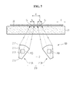
- FIG. 7 is a schematic view illustrating an optical arrangement of an illuminator of a scanner module according to an embodiment
- FIG. 8 is a perspective view of the illuminator of FIG. 7 .
- the illuminator 100 illuminates the document or manuscript board 51 by sending light along a sub-scanning direction (see the Y-direction in FIG. 10 ).
- This sub-scanning direction is substantially perpendicular to an image scanning direction (X-direction) of the scanner module.
- the illuminator may include a light source 200 emitting light, and a light guide unit 210 extending lengthwise in the sub-scanning direction Y and facing the manuscript board 51.
- the light guide unit 210 guides the light toward the object 55 by diffusing the light from the light source 200.
- the light guide unit 210 includes a pair of light guide members 210A and 210B facing the manuscript board 51, and each extend longitudinally along the sub-scan direction (Y-direction as shown in FIG. 8 ) defining the lengths of the light guide units while along the image scan direction (X-direction) the widths of the light guide units 210 are defined.
- the light source 200 may include light emitting diodes capable of emitting light having a wavelength band of three primary colors, namely, red, green and blue.
- the light emitting diodes may be semiconductor devices, an may be capable of generating a sufficient amount of light within a relatively short period of time in comparison to a CCFL or the xenon lamp.
- the start-up time of the scanner module 10 can be shortened and power consumption can be reduced.
- the light emitting diode which is a semiconductor device
- the start-up time of the light source may be shorter in comparison with that a light source utilizing a CCFL which may require the start-up time in excess of, e.g., 30 seconds.
- a light emitting diode may also be advantageous as a light source over a CCFL as unlike a CCFL that is driven at high voltage, e.g., at several hundreds to thousands of voltages, the semiconductor light source can be driven at a low voltage, obviating the need for the use of inverters used for voltage boosting and AC generation.
- the manufacturing cost can be reduced and space utilization can be improved.
- the inverters can be omitted, power consumption can be reduced.
- the semiconductor light source according to an embodiment of the present invention may be capable of relatively stable light output over wider temperature range.
- a semiconductor light source may also reduce the amount of the electromagnetic waves, which may be a source of noise for internal circuits.
- the semiconductor light source of an embodiment of the present invention may be more durable as compared with the CCFL which is made from thin glass material.
- the light emitting diodes may have longer operating life, e.g. of about hundred thousand hours, as compared to a CCFL.
- the light emitting diodes can be fabricated without mercury (Hg) that may present environmental concern.
- light emitting diodes capable of emitting light having a wavelength band of three primary colors are used as the light source 200
- the scope of the application of the present invention is not so limited.
- a white light emitting diode coated with fluorescent material to generate blue color or an ultraviolet ray to generate a white color can also be used as the light source 200.
- various types of point light sources other than a light emitting diode can alternatively be used as the light source 200.
- the light guide members 210A and 210B convert the optical path of light irradiated from the light source 200 such that the light can be irradiated onto at least two regions A 1 and A 2 .
- the light guide members 210A and 210B are spaced apart from each other in the image scan direction.
- the light guide member 210A provided on one side of the image scan direction will be referred to as the first light guide member and the light guide member 210B provided on the other side of the image scan direction will be referred to as the second light guide member.
- the centers C 1 and C 2 of the two regions A 1 and A 2 are spaced apart from each other in the image scan direction X by a distance d. Therefore, the light can be illuminated onto the center C of the object 55 placed on the manuscript board 51 as well as a predetermine region of the object 55 which deviates from the center C of the object 55.
- the illumination device 100 can illuminate the light onto the first and second regions A 1 and A 2 and a pair of light guide members 210A and 210B are provided to guide the light onto the first and second regions A 1 and A 2 .
- the illumination device 100 may further include a holder 230 for guiding the installation position of the light guide members 210A and 210B when the light guide members 210A and 210B are installed in the optical path.
- the light guide members 210A and 210B may have elongated shapes extending in the sub-scan direction Y, and may include transparent materials, such as, e.g., PMMA (polymethyl methacrylate). Each of the light guide members 210A and 210B may have an incident surface 211, a guide surface 213, a reflective surface 215 and an exit surface 217.
- the light from the light source 200 is incident onto the incident surface 211.
- the incident surface 211 is formed on at least one longitudinal end portion of the light guide members 210A and 210B and the light source 200 faces the incident surface 211.
- FIG. 9 shows incident surfaces 211 that are formed on both longitudinal end portions of the light guide members 210A and 210B.
- the light sources 200 are provided to correspond to the incident surfaces 211 formed on both longitudinal end portions of the light guide members 210A and 210B to irradiate light to the incident surfaces 211, thereby increasing the amount of light in the illuminator 100.
- the light guide members 210A and 210B when installed in the holder 230, are slantingly arranged such that the light reflected from the object 55 does not interfere with the light guide members 210A and 210B. That is, as shown in FIG. 7 , the central line of light that is output from the light guide members 210A and 210B is inclined relative to a central optical axis Z of the light.
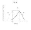
- FIG. 10 is a graph showing light distribution on a surface of a document to be scanned in the width direction of the light guide members 210A and 210B when the light source and the light guide members 210A and 210B are arranged as shown in FIG. 7 .
- reference numeral 251 represents a light distribution curve on the surface of the manuscript placed on the manuscript board 51 when the light is output from the first light guide member 210A
- reference numeral 253 represents a curve showing light distribution on the manuscript board 51 when the light is output from the second light guide member 210B
- reference numeral 255 represents a curve showing the total light distribution on the manuscript board 51.
- the amount of light irradiated onto the manuscript board 51 is maximized at the center C 1 of the first region A 1 and at the center C 2 of the second region A 2 .
- the center C 1 of the first region A 1 is spaced apart from the center C 2 of the second region A 2 by the distance d.
- the amount of light irradiated onto the first and second regions A 1 and A 2 is substantially constant in the region between the center C 1 of the first region A 1 and the center C 2 of the second region A 2 .
- the illumination device 100 having the above structure can illuminate light over a relatively large region of the manuscript as compared with the conventional illumination device.
- the illumination device 100 can be employed in the scanner module 10 capable of performing color scanning operation, and the optical elements constituting the scanner module 10 may have a relatively large assembling tolerance, so that productivity of the scanner module 10 can be improved.
- the scanner module 10 employs the illumination device 100 capable of illuminating light over the relatively large region of the manuscript, so that the output value of the image sensor 130 may remain uniform despite possible deviations in positioning of the reflection mirrors 140 and the focus lens 120 during assembly of the illumination device 100.
- the exit surface 217 faces the manuscript board 51.
- the light that is diffused and reflected by the reflective surface 215 and the guide surface 213 may be output through the exit surface 217.
- the exit surface 217 may function as a condenser lens that focuses the light on the manuscript board 51, so that light illuminated in the first region A 1 may have a Gaussian distribution.
- the exit surface 217 is provided as a convex lens having an arc-shape section with a predetermined curvature.
- the reflective surface 215 is disposed in opposition to the exit surface 217 so as to diffuse and reflect the light incident through the incident surface 211, thereby allowing the light to be uniformly output through the entire surface of the exit surface 217. To this end, the light is preferably subject to scattered reflection over the entire area of the reflective surface 215.
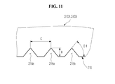
- the reflective surface 215 may be formed with a plurality of reflective grooves 215a and 215b so that the light from the light source 200 is subject to a scattered reflection.
- the reflective grooves 215a and 215b may have triangular sectional shapes to guide the light received from the light source 200 through the incident surface 211 at longitudinal end portions of the light guide members 210A and 210B toward the exit surface 217 of the light guide members 210A and 210B.
- the amount of light reflected toward the exit surface 217 of the light guide members 210A and 210B by the reflective grooves 215a and 215b may increase proportionally to the height H of the triangular section of the reflective grooves 215a and 215b and to the inclination angle ⁇ 1 of the lateral side of the triangular section. Therefore, the amount of light irradiated from the light guide members 210A and 210B can be adjusted by properly adjusting the height H and the inclination angle ⁇ 1 of the triangular section of the reflective grooves 215a and 215b.
- the present invention is not so limited.
- the reflective grooves 215a and 215b may also have arc-shaped sections or rectangular-shaped sections.
- the reflective surface 215 of the light guide members 210A and 210B may be formed with first and second reflective grooves 215a and 215b, which are symmetrically formed while being inclined along the widths of light guide members 210A and 210B.
- the first and second reflective grooves 215a and 215b may cross each other on the reflective surface 215.
- the light irradiated from the light source 200 can be guided toward the exit surface 217 of the light guide members 210A and 210B while being diffused in the lateral direction by the first and second reflective grooves 215a and 215b, so that the light can be uniformly distributed in the width direction of the light guide members 210A and 210B when the light is received through the incident surfaces 211 at longitudinal end portions of the light guide members 210A and 21 0B.
- the amount of light diffused in the width direction of the light guide members 210A and 210B may increase proportionally to the inclination angle of the first and second reflective grooves 215a and 215b.
- FIG. 13 is a graph of light distribution curve on across the width of a manuscript board 51 when the light is illuminated with the light guide members 210A and 210B having the first and second reflective grooves 215a and 215b, which are symmetrically patterned while being non-parallel with respect to each other, and when the light irradiated from the longitudinal end portions of the light guide members 210A and 210B is emitted through the exit surface 217.
- the reflective surface 215 may be provided with a micro-lens shape or a cylindrical shape.
- the reflective surface 215 can scatter the incident light, so that the light can be uniformly output through the exit surface 217.
- a light diffusion material such as a white pigment, can be coated on the reflective surface 215 such that light can be uniformly irradiated from the exit surface 217.
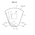
- the guide surface 213 is formed on both sides of the light guide members 210A and 210b in order to guide the incident light, which is incident into the incident surface 211, such that the incident light can be irradiated through substantially the entire area of the exit surface 217 by internal total reflection.
- a plurality of guide surfaces 213 are symmetrically formed at both sides of the light guide members 210A and 210b to reflect the light, which is reflected from the reflective surface 215 at various reflection angles, toward the exit surface of the light guide members 210A and 210b. If the plural guide surfaces 213 are symmetrically formed on both sides of the light guide members 210A and 210b, most of the light reflected from the reflective surface 215 may be guided toward the exit surface 217 of the light guide members 210A and 210b while being reflected by the guide surfaces 213, so that the amount of light leaked out of the light guide members 210A and 210b through the guide surfaces 213 can be reduced.
- the guide surfaces 213 may serve as a virtual light source together with the reflective surface 215. Therefore, the light distribution on the surface of the manuscript can be adjusted by properly adjusting the angle of guide surfaces 213 when the light is irradiated through the exit surface 217 of the light guide members 210A and 210b.
- the guide surfaces 213 may include a first guide surface 213a, which extends from both sides of the reflective surface 215 while forming an obtuse angle relative to the reflective surface 215, and a second guide surface 213b, which extends from the first guide surface 213a while forming an obtuse angle relative to the first guide surface 213a.
- the first and second guide surfaces 213a and 213b are formed on both sides of the light guide members 210A and 210b, the light reflected from the reflective surface 215 at a relatively large reflection angle can be reflected toward the exit surface 217 of the light guide members 210A and 210b by the first guide surface 213a, and the light reflected from the reflective surface 215 at a relatively small reflection angle can be reflected toward the exit surface 217 of the light guide members 210A and 210b by the second guide surface 213b, so that the amount of light leaked out of the light guide members 210A and 210b can be reduced.
- the incident angle of the light incident onto the first and second guide surfaces 213a and 213b from the reflective surface 215 is desirably greater than a critical incident angle ⁇ 2 that ensures total reflection of the light.
- the angle between the reflective surface 215 and the first guide surface 213a is equal to or greater than the sum of the critical incident angle ⁇ 2 that ensures total reflection of the light and an angle of 90°.
- the angle between the first guide surface 213a and the second guide surface 213b may also be designed such that the incident angle of the light, which is incident onto the second guide surface 213b from the reflective surface 215, may be equal to or greater than the critical incident angle ⁇ 2. Since the minimum incident angle of the light incident on the second guide surface 213b may correspond to an angle between a virtual line L (shown in FIG.
- the angle between the virtual line L and the second guide surface 213b may preferably be equal to or greater than the sum of the critical incident angle ⁇ 2 and an angle of 90°.
- the light guide members 210A and 210B may be formed with polymethyl methacrylate, the critical incident angle ⁇ 2 of which may be 41.8°. Therefore, the angle between the reflective surface 215 and the first guide surface 213a and the angle between the virtual line L and the second guide surface 213b mat be made to be equal to or greater than 131.8°.
- the angle between the reflective surface 215 and the first guide surface 213a, and the angle between the virtual line L and the second guide surface 213b are both described as being equal to or greater than ⁇ 2 plus 90°, since the light may be subject to Lambertian reflection at the reflective surface 215, the amount of light incident on the first guide surface 213a may be relatively small.
- the scattering reflection and the uniform light distribution may be achieved by setting only the angle between the virtual line L and the second guide surface 213b greater than the sum of the critical incident angle ⁇ 2 and an angle of 90°.
- the light guide members 210A and 210B may be formed with material other than polymethyl methacrylate.
- the light guide members 210A and 210B may alternatively formed with colorless transparent resin.
- the critical incident angle according to the type of resins can be calculated using Snell's law.
- FIG. 15 is a block diagram of the image scanning apparatus according an embodiment of the present invention.
- the image scanning apparatus may include the scanner module 10e and an image processing unit 20 which processes the image obtained from the scanner module 10.
- the image scanning apparatus of the present invention may include an MFP (multi-function printer), a copy machine, a facsimile machine, a scanner, or the like.
- the image processing unit 20 may include at least one of a file forming unit 21 for forming an image file based on the image obtained from the image sensor of the scanner module 10 and an image forming unit 25 for forming an image on a printing medium based on the image obtained from the image sensor.
- the file forming unit 21 may be a microprocessor, microcontroller or the like, that includes a CPU to execute one or more computer instructions to implement the operation of forming the image files from the image data received from the image sensor of the scanner module 10, and may further include a memory device, e.g., a Random Access Memory (RAM), Read-Only-Memory (ROM), a flesh memory, or the like, to store the one or more computer instructions.
- a memory device e.g., a Random Access Memory (RAM), Read-Only-Memory (ROM), a flesh memory, or the like, to store the one or more computer instructions.
- the image forming unit may include any of various printing mechanisms, e.g., one utilizing electro-photographic image forming technique, which may include photosensitive member to which latent images are formed, and the latent image of which is developed into a toner image that is transferred and fixed on a printing medium, e.g., a sheet of paper, one that utilizes ink jet technique including an ink jet print head that places tiny ink droplets through nozzles of the print head directly on the paper, or the like.
- a printing medium e.g., a sheet of paper
- ink jet technique including an ink jet print head that places tiny ink droplets through nozzles of the print head directly on the paper, or the like.
- the image scanning apparatus employs the scanner module 10 having the illumination device 100 described above, the image sensors aligned in a plurality of rows can output uniform values even if the position of optical elements, such as reflection mirrors, becomes out of alignment by various external parameters.
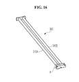
- a pair of light guide members 310A and 310B may be extruded as an integral body, e.g., by using a single mold.
- FIG. 16 illustrates a structure in which a first light guiding member 310A and a second light guiding member 310B may be connected at opposite ends thereof.
- the first light guiding member 310A and the second light guiding member 310A are extruded as an integrally formed body or from the same single mold, e.g., through an injection molding process, and are assembled together.
- the light source which irradiates light toward the light guide members 310A and 310B, may also be integrally formed with a single substrate 360.
- a coupling structure 370 may be provided between the light source substrate 360 and the light guide members 310A and 310B to improve assembling process for the illumination device 100. This extrusion and simultaneous assembly as described above may help to further alleviate the problem of assembling tolerance, simplify assembling work, and decrease production costs.
- first and second guide surfaces 213a and 213b are shown in FIG. 14 as having linear cross-sectional shapes, the present invention is not so limited.
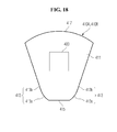
- a first guide surface 413a of light guide member 410A and/or 410B may have a curved shape and a second guide surface 413b of the light guide members 410A and 410B may have a linear sectional shape.
- a reflective member 535 is formed on at least one of a reflective surface 515 and a guide surface 513 of light guide members 510A and 510B.
- the reflective member 535 is formed on the guide surface 513 and the reflective surface 515, respectively.
- the reflective member 535 may be obtained by forming the reflective groove structure on the guide surface 513 or the reflective surface 515 as previously described, or, for example, by coating or printing the guide surface 513 or the reflective surface 515 with a material having high reflectivity of about 90% or more in the wavelength band of the light irradiated from the light source 500. Such material having high reflectivity is generally known in the art, and thus is no described in detailed herein for the sake of brevity.
- FIG. 7 shows the exit surface 217 in the form of the convex lens having an arcuate shape
- the present invention is not so limited.
- the exit surface may be prepared in the form of a flat lens having a plane shape or a Fresnel lens pattern.
- FIG. 9 shows the incident surface 211 formed at both longitudinal end portions of the light guide members 210A and 210B
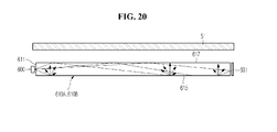
- a light source 600 may be installed only at one longitudinal end portion of light guide members 610A and/or 610B, so that only one incident surface 611 may be formed on one longitudinal end portion of light guide members 610A and/or 610B.
- a reflective plate 631 may be provided at the other longitudinal end portion of light guide members 610A and/or 610B.
- FIG. 12 shows the first and second reflective grooves 215a and 215b that cross each other as one possible illustrative pattern thereof, the present invention is not so limited.
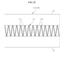
- first and second reflective grooves 711 a and 711 b of a reflective surface 711 may be patterned not to cross each other, but are alternately arranged along the light guide members 710A and 710B, achieving the same beneficial aspects contemplated by the present disclosure.
- first and second reflective grooves 215a and 215b are described to have the same inclination angle across the length of the light guide members.
- the light distribution on the surface of the manuscript may not be uniform in the width direction of the light guide members 210A and 210B at the vicinity of the longitudinal end portions of the light guide members 210A and 210B.
- the inclination angle of first and second reflective grooves 811 a and 811 b formed in a reflective surface 811 may gradually increase from the center towards the ends of light guide members 810A and 810B. In this case, light can be effectively diffused even at the end portiions of the light guide members 810A and 810B.
- the amount of light radiated from the both longitudinal ends of the light guide members 810A and 810B may increase proportionally to the inclination angle of the first and second reflective grooves 811 a and 811 b formed in the light guide members 810A and 810B. Therefore, if the inclination angle of the first and second reflective grooves 811a and 811b is gradually increased from the center towards the ends of light guide members 810A and 810B as described above, the amount of light irradiated onto the object 55 from the both longitudinal ends of the light guide members 810A and 810B may increase.
- the inclination angle of the first and second reflective grooves 911 a and 911 b gradually increases from the center to the both ends of light guide members 910A and 910B, and at the same time, the interval between the first and second reflective grooves 911 a and 911b increases proportionally to the inclination angle of the first and second reflective grooves 911 a and 911 b.
- the amount of light radiated onto the object from the both longitudinal ends of the light guide members 910A and 910B may be reduced, so the difference between the amount of light irradiated onto the object 55 from the center of the light guide members 910A and 910B and the amount of light irradiated onto the object 55 from the both longitudinal ends of the light guide members 910A and 910B can be reduced.
- the present invention can also be applied to an MMT (mirror moving type), in which one light source and one reflection mirror are integrated in a single module and two reflection mirrors are integrated in another single module such that the modules including the mirrors can read the image while moving along the object.
- MMT mirror moving type
Landscapes
- Engineering & Computer Science (AREA)
- Multimedia (AREA)
- Physics & Mathematics (AREA)
- Signal Processing (AREA)
- Optics & Photonics (AREA)
- General Physics & Mathematics (AREA)
- Theoretical Computer Science (AREA)
- Facsimile Scanning Arrangements (AREA)
- Light Sources And Details Of Projection-Printing Devices (AREA)
- Facsimile Heads (AREA)
- Facsimiles In General (AREA)
Applications Claiming Priority (1)
| Application Number | Priority Date | Filing Date | Title |
|---|---|---|---|
| KR1020070069502A KR101279034B1 (ko) | 2007-07-11 | 2007-07-11 | 스캐너 모듈 및 이를 채용한 화상독취장치 |
Publications (2)
| Publication Number | Publication Date |
|---|---|
| EP2015556A2 true EP2015556A2 (de) | 2009-01-14 |
| EP2015556A3 EP2015556A3 (de) | 2009-07-15 |
Family
ID=39870679
Family Applications (1)
| Application Number | Title | Priority Date | Filing Date |
|---|---|---|---|
| EP08160134A Ceased EP2015556A3 (de) | 2007-07-11 | 2008-07-10 | Mehrzweckgerät mit Scannermodul und Bildscanvorrichtung mit dem Scannermodul |
Country Status (5)
| Country | Link |
|---|---|
| US (2) | US8228567B2 (de) |
| EP (1) | EP2015556A3 (de) |
| JP (1) | JP5670014B2 (de) |
| KR (1) | KR101279034B1 (de) |
| CN (1) | CN101415056A (de) |
Families Citing this family (36)
| Publication number | Priority date | Publication date | Assignee | Title |
|---|---|---|---|---|
| US8059168B2 (en) * | 2005-03-14 | 2011-11-15 | Gtech Corporation | System and method for scene change triggering |
| US8072651B2 (en) * | 2005-03-14 | 2011-12-06 | Gtech Corporation | System and process for simultaneously reading multiple forms |
| US8233200B2 (en) * | 2005-03-14 | 2012-07-31 | Gtech Corporation | Curvature correction and image processing |
| US7852523B2 (en) * | 2007-07-11 | 2010-12-14 | Samsung Electronics Co., Ltd. | Scanner module and image scanning apparatus employing the same |
| US7924478B2 (en) * | 2007-07-11 | 2011-04-12 | Samsung Electronics Co., Ltd. | Scanner module and image scanning apparatus employing the same |
| KR101279034B1 (ko) | 2007-07-11 | 2013-07-02 | 삼성전자주식회사 | 스캐너 모듈 및 이를 채용한 화상독취장치 |
| US8379275B2 (en) * | 2007-07-31 | 2013-02-19 | Samsung Electronics Co., Ltd. | Scanner module and image scanning apparatus employing the same |
| US8358447B2 (en) | 2007-07-31 | 2013-01-22 | Samsung Electronics Co., Ltd. | Scanner module and image scanning apparatus employing the same |
| EP2395738B1 (de) | 2007-07-31 | 2016-03-23 | Samsung Electronics Co., Ltd. | Mehrzweckvorrichtung mit Scannermodul und Bildscanvorrichtung mit dem Scannermodul |
| TW201101798A (en) * | 2009-06-30 | 2011-01-01 | E Pin Optical Industry Co Ltd | Tetra-mirror multi-reflection scanning module |
| JP5293479B2 (ja) * | 2009-07-17 | 2013-09-18 | 富士ゼロックス株式会社 | 画像読取装置及び画像形成装置 |
| JP4757340B2 (ja) | 2009-10-30 | 2011-08-24 | シャープ株式会社 | 照明装置、その照明装置を備える画像読取り装置、その画像読取り装置を備える画像形成装置 |
| JP5573107B2 (ja) * | 2009-11-04 | 2014-08-20 | ウシオ電機株式会社 | 照明装置 |
| KR101364848B1 (ko) | 2009-12-28 | 2014-02-19 | 케논 콤포넨트 가부시키가이샤 | 밀착형 이미지 센서 유닛, 및 그것을 사용한 화상 판독 장치 |
| WO2011096411A1 (ja) * | 2010-02-05 | 2011-08-11 | 株式会社 東芝 | 照明装置、及び照明装置を備える画像読取装置 |
| JP5126279B2 (ja) | 2010-04-26 | 2013-01-23 | コニカミノルタビジネステクノロジーズ株式会社 | 画像読取装置 |
| JP5139507B2 (ja) | 2010-12-10 | 2013-02-06 | キヤノン・コンポーネンツ株式会社 | イメージセンサユニット、及び、画像読取装置 |
| JP5204207B2 (ja) | 2010-12-17 | 2013-06-05 | キヤノン・コンポーネンツ株式会社 | イメージセンサユニットおよびそれを用いた画像読取装置 |
| JP5244952B2 (ja) | 2010-12-21 | 2013-07-24 | キヤノン・コンポーネンツ株式会社 | イメージセンサユニット、及び、画像読取装置 |
| JP5384471B2 (ja) | 2010-12-28 | 2014-01-08 | キヤノン・コンポーネンツ株式会社 | イメージセンサユニット、及び、画像読取装置 |
| JP5729542B2 (ja) * | 2011-01-11 | 2015-06-03 | 株式会社リコー | ライン照明光学系、及び画像読取装置 |
| US8493637B2 (en) * | 2011-01-21 | 2013-07-23 | Seiko Epson Corporation | Image forming optical element, image forming optical array, and image reading device |
| JP2012199764A (ja) * | 2011-03-22 | 2012-10-18 | Konica Minolta Business Technologies Inc | 画像読み取り装置 |
| JP5400188B2 (ja) * | 2011-05-11 | 2014-01-29 | キヤノン・コンポーネンツ株式会社 | イメージセンサユニットおよびそれを用いた画像読取装置、画像形成装置 |
| JP5422604B2 (ja) * | 2011-05-31 | 2014-02-19 | 京セラドキュメントソリューションズ株式会社 | 画像読取装置及びこれを備えた画像形成装置 |
| JP2013078102A (ja) * | 2011-06-17 | 2013-04-25 | Rohm Co Ltd | イメージセンサモジュール |
| JP5518953B2 (ja) * | 2011-08-09 | 2014-06-11 | キヤノン・コンポーネンツ株式会社 | イメージセンサユニットおよび画像読取装置 |
| CN102710884B (zh) * | 2012-03-16 | 2014-05-21 | 苏州佳世达电通有限公司 | 扫描装置 |
| JP2014123941A (ja) | 2012-11-21 | 2014-07-03 | Canon Inc | 照明装置および画像読取装置 |
| KR102012890B1 (ko) * | 2013-03-25 | 2019-08-21 | 휴렛-팩커드 디벨롭먼트 컴퍼니, 엘.피. | 스캔 대상물의 위치에 따른 기능 수행 방법 및 이를 수행하기 위한 화상형성장치 |
| AP2016009037A0 (en) * | 2013-04-21 | 2016-02-29 | Mobileoct Ltd | Polarized light imaging apparatus and methods thereof for separating light from a surface of a sample its deeper diffuse layers |
| JP5915639B2 (ja) * | 2013-12-25 | 2016-05-11 | コニカミノルタ株式会社 | 導光体、導光装置及び画像読取装置 |
| CN107347257B (zh) * | 2015-02-20 | 2019-08-20 | 三菱电机株式会社 | 导光体、光源装置及图像读取装置 |
| JP2016171423A (ja) * | 2015-03-12 | 2016-09-23 | キヤノン株式会社 | 画像読取装置 |
| JP6540425B2 (ja) * | 2015-09-25 | 2019-07-10 | ウシオ電機株式会社 | 線状光源装置 |
| CN110313168B (zh) * | 2017-02-22 | 2022-03-22 | 三菱电机株式会社 | 照明装置及图像读取装置 |
Citations (6)
| Publication number | Priority date | Publication date | Assignee | Title |
|---|---|---|---|---|
| JPH06178050A (ja) * | 1992-12-08 | 1994-06-24 | Ricoh Co Ltd | 画像読み取り装置 |
| US6127675A (en) * | 1995-08-24 | 2000-10-03 | Matsushita Electric Industrial Co., Ltd. | Linear illumination device |
| US20020054387A1 (en) * | 2000-08-11 | 2002-05-09 | Masahiko Yokota | Image sensor and image reading apparatus |
| US20020131275A1 (en) * | 2001-01-16 | 2002-09-19 | Estec Co., Ltd. | LED illuminating device and lighting apparatus employing the same |
| US20040071436A1 (en) * | 2002-08-07 | 2004-04-15 | Samsung Electronics Co., Ltd. | Optical guide and image forming apparatus using the same |
| JP2004170858A (ja) | 2002-11-22 | 2004-06-17 | Canon Inc | 画像読取装置 |
Family Cites Families (46)
| Publication number | Priority date | Publication date | Assignee | Title |
|---|---|---|---|---|
| GB1394572A (en) * | 1971-11-22 | 1975-05-21 | Secr Defence | Facsimile scanning apparatus |
| JPH02226626A (ja) | 1989-02-27 | 1990-09-10 | Omron Tateisi Electron Co | 色識別光センサ |
| JPH06208066A (ja) * | 1993-01-08 | 1994-07-26 | Fuji Xerox Co Ltd | 光学走査装置 |
| JP2693098B2 (ja) * | 1993-01-19 | 1997-12-17 | キヤノン株式会社 | 導光体、導光体を有する照明装置、照明装置を有する読取装置及び画像処理システム |
| KR0158247B1 (ko) * | 1993-01-19 | 1999-03-20 | 미따라이 하지메 | 도광체와, 이 도광체를 갖는 조명 장치, 그리고 이 조명 장치를 갖는 화상 판독장치 및 정보 처리 장치 |
| JP3334833B2 (ja) * | 1995-08-24 | 2002-10-15 | 松下電器産業株式会社 | 線状照明装置 |
| US5483053A (en) * | 1994-09-27 | 1996-01-09 | Hewlett-Packard Company | Variable resolution color image scanner having an exposure delay between successive linear photosensors detecting different colors |
| JPH08152771A (ja) * | 1994-11-28 | 1996-06-11 | Sharp Corp | デジタル複写機 |
| JP3176303B2 (ja) | 1996-02-09 | 2001-06-18 | キヤノン株式会社 | 信号処理装置 |
| TW383508B (en) | 1996-07-29 | 2000-03-01 | Nichia Kagaku Kogyo Kk | Light emitting device and display |
| GB9618720D0 (en) * | 1996-09-07 | 1996-10-16 | Philips Electronics Nv | Electrical device comprising an array of pixels |
| US5850585A (en) * | 1996-10-16 | 1998-12-15 | Mita Industrial Co., Ltd. | Destaticizer and image forming apparatus employing the same |
| JP3453488B2 (ja) | 1996-12-27 | 2003-10-06 | キヤノン株式会社 | 照明装置及びこれを用いた画像読み取り装置 |
| JP3167111B2 (ja) | 1997-04-25 | 2001-05-21 | キヤノン株式会社 | 画像読取装置 |
| JP3999315B2 (ja) * | 1997-08-29 | 2007-10-31 | ローム株式会社 | イメージセンサ基板、およびこれを用いたイメージセンサ |
| JP2000115470A (ja) | 1998-10-08 | 2000-04-21 | Canon Inc | 原稿読取装置 |
| JP3618056B2 (ja) * | 1999-02-23 | 2005-02-09 | 理想科学工業株式会社 | 画像処理装置 |
| US6206534B1 (en) | 1999-04-09 | 2001-03-27 | Cmos Sensor, Inc. | Illumination device for use in image reading applications |
| EP1103759A3 (de) | 1999-11-11 | 2005-02-23 | Toyoda Gosei Co., Ltd. | Vollfarben-Lichtquellen-Einheit |
| TW503646B (en) * | 2000-03-16 | 2002-09-21 | Nippon Sheet Glass Co Ltd | Line illuminating device |
| JP2002135533A (ja) | 2000-10-19 | 2002-05-10 | Ricoh Co Ltd | 画像読取装置用のキャリッジ |
| JP2003046735A (ja) * | 2001-08-02 | 2003-02-14 | Seiko Epson Corp | 画像読み取り装置における焦点合わせ方法 |
| JP2003134307A (ja) | 2001-10-26 | 2003-05-09 | Canon Inc | 画像読取装置 |
| US6641281B2 (en) | 2002-04-09 | 2003-11-04 | Teco Image Systems Co., Ltd. | Lamp tube support structure |
| US7233419B2 (en) * | 2002-10-08 | 2007-06-19 | Chin-Lin Chang | Scanner having a self collection light source |
| JP4104064B2 (ja) * | 2003-01-16 | 2008-06-18 | ローム株式会社 | 画像読み取り装置 |
| JP4170818B2 (ja) | 2003-04-11 | 2008-10-22 | 株式会社リコー | 照明装置・原稿読み取り装置・画像形成装置 |
| WO2005001528A1 (ja) | 2003-06-25 | 2005-01-06 | Nippon Sheet Glass Co., Ltd. | 導光体および画像読取装置 |
| EP1511289B1 (de) | 2003-08-19 | 2011-11-23 | Ricoh Company, Ltd. | Beleuchtungsanordnung, Bildlesevorrichtung und Bilderzeugungsgerät |
| JP2005123675A (ja) * | 2003-10-14 | 2005-05-12 | Mitsubishi Electric Corp | 画像読み取り装置照明光学系 |
| JP2005198106A (ja) | 2004-01-08 | 2005-07-21 | Nippon Sheet Glass Co Ltd | ライン照明装置および画像読取装置 |
| JP4093990B2 (ja) * | 2004-05-26 | 2008-06-04 | 日本板硝子株式会社 | 導光体、ライン照明装置および画像読取装置 |
| US7733543B2 (en) * | 2004-10-18 | 2010-06-08 | Ricoh Company, Ltd. | Document illumination apparatus, document reading apparatus and image forming apparatus permitting efficient cooling |
| US7593143B2 (en) * | 2005-03-31 | 2009-09-22 | Xerox Corporation | Compound curved concentrator based illuminator |
| JPWO2006120932A1 (ja) * | 2005-05-12 | 2008-12-18 | 日本板硝子株式会社 | 導光体及び画像読取装置 |
| JP4438713B2 (ja) | 2005-07-25 | 2010-03-24 | ブラザー工業株式会社 | 画像読取装置 |
| JP2007150634A (ja) | 2005-11-25 | 2007-06-14 | Kyocera Mita Corp | 画像読取装置および画像形成装置 |
| JP2006148956A (ja) | 2005-12-21 | 2006-06-08 | Nippon Sheet Glass Co Ltd | ライン照明装置及び画像読取装置 |
| JP4788577B2 (ja) * | 2006-11-10 | 2011-10-05 | ソニー株式会社 | ライトガイド、光源装置及び電子機器 |
| US7502148B2 (en) | 2007-02-16 | 2009-03-10 | Cmos Sensor, Inc. | Multiple lightguide electronic document imaging device |
| TW200905369A (en) * | 2007-02-26 | 2009-02-01 | Rohm Co Ltd | Linear light source apparatus and image reading apparatus provided with the same |
| US7864381B2 (en) * | 2007-03-20 | 2011-01-04 | Xerox Corporation | Document illuminator with LED-driven phosphor |
| KR101279034B1 (ko) | 2007-07-11 | 2013-07-02 | 삼성전자주식회사 | 스캐너 모듈 및 이를 채용한 화상독취장치 |
| US7924478B2 (en) | 2007-07-11 | 2011-04-12 | Samsung Electronics Co., Ltd. | Scanner module and image scanning apparatus employing the same |
| JP2009212745A (ja) * | 2008-03-04 | 2009-09-17 | Fuji Xerox Co Ltd | 画像読み取り装置 |
| JP5573107B2 (ja) * | 2009-11-04 | 2014-08-20 | ウシオ電機株式会社 | 照明装置 |
-
2007
- 2007-07-11 KR KR1020070069502A patent/KR101279034B1/ko not_active Expired - Fee Related
-
2008
- 2008-07-10 EP EP08160134A patent/EP2015556A3/de not_active Ceased
- 2008-07-10 CN CNA2008101756735A patent/CN101415056A/zh active Pending
- 2008-07-10 US US12/170,922 patent/US8228567B2/en not_active Expired - Fee Related
- 2008-07-10 JP JP2008180567A patent/JP5670014B2/ja not_active Expired - Fee Related
-
2012
- 2012-07-18 US US13/551,784 patent/US9225866B2/en not_active Expired - Fee Related
Patent Citations (6)
| Publication number | Priority date | Publication date | Assignee | Title |
|---|---|---|---|---|
| JPH06178050A (ja) * | 1992-12-08 | 1994-06-24 | Ricoh Co Ltd | 画像読み取り装置 |
| US6127675A (en) * | 1995-08-24 | 2000-10-03 | Matsushita Electric Industrial Co., Ltd. | Linear illumination device |
| US20020054387A1 (en) * | 2000-08-11 | 2002-05-09 | Masahiko Yokota | Image sensor and image reading apparatus |
| US20020131275A1 (en) * | 2001-01-16 | 2002-09-19 | Estec Co., Ltd. | LED illuminating device and lighting apparatus employing the same |
| US20040071436A1 (en) * | 2002-08-07 | 2004-04-15 | Samsung Electronics Co., Ltd. | Optical guide and image forming apparatus using the same |
| JP2004170858A (ja) | 2002-11-22 | 2004-06-17 | Canon Inc | 画像読取装置 |
Also Published As
| Publication number | Publication date |
|---|---|
| JP2009022007A (ja) | 2009-01-29 |
| KR20090006304A (ko) | 2009-01-15 |
| US20090015883A1 (en) | 2009-01-15 |
| US8228567B2 (en) | 2012-07-24 |
| CN101415056A (zh) | 2009-04-22 |
| KR101279034B1 (ko) | 2013-07-02 |
| US9225866B2 (en) | 2015-12-29 |
| EP2015556A3 (de) | 2009-07-15 |
| US20130016385A1 (en) | 2013-01-17 |
| JP5670014B2 (ja) | 2015-02-18 |
Similar Documents
| Publication | Publication Date | Title |
|---|---|---|
| US8228567B2 (en) | Multi-functional device having scanner module and image scanning apparatus employing the scanner module | |
| US7924478B2 (en) | Scanner module and image scanning apparatus employing the same | |
| JP4093990B2 (ja) | 導光体、ライン照明装置および画像読取装置 | |
| US7852523B2 (en) | Scanner module and image scanning apparatus employing the same | |
| US6193383B1 (en) | Linear light source unit | |
| CN103907337B (zh) | 照明单元以及使用该照明单元的图像读取装置 | |
| CN102661531B (zh) | 照明单元、图像读取装置和图像形成装置 | |
| JP2004056425A (ja) | ライン照明装置及び画像読取装置 | |
| US9167121B2 (en) | Lighting unit and image scanner using same | |
| JP5533505B2 (ja) | 線状光源 | |
| US6612730B1 (en) | Rod-shaped light guide and illuminating device incorporating rod-shaped light guide | |
| CN101867676A (zh) | 照明装置以及图像读取装置 | |
| US20110164412A1 (en) | LED linear light source and reading apparatus | |
| JP3139822U (ja) | 走査装置 | |
| US8867109B2 (en) | Light guide, illumination device, and image reading apparatus | |
| US7760434B2 (en) | Document illuminator with surface lens | |
| JP2006148956A (ja) | ライン照明装置及び画像読取装置 | |
| KR101391792B1 (ko) | 화상독취장치 및 이를 갖춘 화상형성기기 | |
| JP2025099261A (ja) | 照明装置及びそれを用いた画像読取装置 | |
| JP5239232B2 (ja) | 画像読取装置および画像形成装置 | |
| JPWO2019003480A1 (ja) | 導光体及び画像読取装置 |
Legal Events
| Date | Code | Title | Description |
|---|---|---|---|
| PUAI | Public reference made under article 153(3) epc to a published international application that has entered the european phase |
Free format text: ORIGINAL CODE: 0009012 |
|
| AK | Designated contracting states |
Kind code of ref document: A2 Designated state(s): AT BE BG CH CY CZ DE DK EE ES FI FR GB GR HR HU IE IS IT LI LT LU LV MC MT NL NO PL PT RO SE SI SK TR |
|
| AX | Request for extension of the european patent |
Extension state: AL BA MK RS |
|
| PUAL | Search report despatched |
Free format text: ORIGINAL CODE: 0009013 |
|
| AK | Designated contracting states |
Kind code of ref document: A3 Designated state(s): AT BE BG CH CY CZ DE DK EE ES FI FR GB GR HR HU IE IS IT LI LT LU LV MC MT NL NO PL PT RO SE SI SK TR |
|
| AX | Request for extension of the european patent |
Extension state: AL BA MK RS |
|
| 17P | Request for examination filed |
Effective date: 20090615 |
|
| 17Q | First examination report despatched |
Effective date: 20090818 |
|
| AKX | Designation fees paid |
Designated state(s): DE FR GB NL |
|
| RAP1 | Party data changed (applicant data changed or rights of an application transferred) |
Owner name: SAMSUNG ELECTRONICS CO., LTD. |
|
| RAP1 | Party data changed (applicant data changed or rights of an application transferred) |
Owner name: S-PRINTING SOLUTION CO., LTD. |
|
| RAP1 | Party data changed (applicant data changed or rights of an application transferred) |
Owner name: HP PRINTING KOREA CO., LTD. |
|
| STAA | Information on the status of an ep patent application or granted ep patent |
Free format text: STATUS: THE APPLICATION HAS BEEN REFUSED |
|
| 18R | Application refused |
Effective date: 20180410 |