EP2011206B1 - Vcsel with photonic crystal mirror for waveguiding by diffraction - Google Patents
Vcsel with photonic crystal mirror for waveguiding by diffraction Download PDFInfo
- Publication number
- EP2011206B1 EP2011206B1 EP07741454A EP07741454A EP2011206B1 EP 2011206 B1 EP2011206 B1 EP 2011206B1 EP 07741454 A EP07741454 A EP 07741454A EP 07741454 A EP07741454 A EP 07741454A EP 2011206 B1 EP2011206 B1 EP 2011206B1
- Authority
- EP
- European Patent Office
- Prior art keywords
- photonic crystal
- light
- crystal layer
- substrate
- layer
- Prior art date
- Legal status (The legal status is an assumption and is not a legal conclusion. Google has not performed a legal analysis and makes no representation as to the accuracy of the status listed.)
- Not-in-force
Links
- 239000004038 photonic crystal Substances 0.000 title claims abstract description 60
- 239000000758 substrate Substances 0.000 claims abstract description 40
- 239000011148 porous material Substances 0.000 claims description 15
- 230000003287 optical effect Effects 0.000 claims description 11
- RKTYLMNFRDHKIL-UHFFFAOYSA-N copper;5,10,15,20-tetraphenylporphyrin-22,24-diide Chemical compound [Cu+2].C1=CC(C(=C2C=CC([N-]2)=C(C=2C=CC=CC=2)C=2C=CC(N=2)=C(C=2C=CC=CC=2)C2=CC=C3[N-]2)C=2C=CC=CC=2)=NC1=C3C1=CC=CC=C1 RKTYLMNFRDHKIL-UHFFFAOYSA-N 0.000 claims description 5
- 230000007547 defect Effects 0.000 claims description 4
- 238000000605 extraction Methods 0.000 claims description 4
- 230000000737 periodic effect Effects 0.000 abstract description 8
- 230000010355 oscillation Effects 0.000 description 11
- VYPSYNLAJGMNEJ-UHFFFAOYSA-N Silicium dioxide Chemical compound O=[Si]=O VYPSYNLAJGMNEJ-UHFFFAOYSA-N 0.000 description 8
- 238000013461 design Methods 0.000 description 6
- 239000004065 semiconductor Substances 0.000 description 6
- 239000000463 material Substances 0.000 description 5
- 229910052681 coesite Inorganic materials 0.000 description 4
- 229910052906 cristobalite Inorganic materials 0.000 description 4
- 239000000377 silicon dioxide Substances 0.000 description 4
- 229910052682 stishovite Inorganic materials 0.000 description 4
- 229910052905 tridymite Inorganic materials 0.000 description 4
- 238000003475 lamination Methods 0.000 description 3
- 238000000034 method Methods 0.000 description 3
- 229910001218 Gallium arsenide Inorganic materials 0.000 description 2
- 229910003910 SiCl4 Inorganic materials 0.000 description 1
- 230000009471 action Effects 0.000 description 1
- 230000003321 amplification Effects 0.000 description 1
- 238000013459 approach Methods 0.000 description 1
- 230000004888 barrier function Effects 0.000 description 1
- 230000008901 benefit Effects 0.000 description 1
- 230000008859 change Effects 0.000 description 1
- 230000001427 coherent effect Effects 0.000 description 1
- 238000011161 development Methods 0.000 description 1
- 230000018109 developmental process Effects 0.000 description 1
- 230000005672 electromagnetic field Effects 0.000 description 1
- 238000010894 electron beam technology Methods 0.000 description 1
- 238000002347 injection Methods 0.000 description 1
- 239000007924 injection Substances 0.000 description 1
- 238000004519 manufacturing process Methods 0.000 description 1
- 238000002488 metal-organic chemical vapour deposition Methods 0.000 description 1
- 238000012986 modification Methods 0.000 description 1
- 230000004048 modification Effects 0.000 description 1
- 238000003199 nucleic acid amplification method Methods 0.000 description 1
- 238000001020 plasma etching Methods 0.000 description 1
- 230000005855 radiation Effects 0.000 description 1
- 238000011160 research Methods 0.000 description 1
- 239000011347 resin Substances 0.000 description 1
- 229920005989 resin Polymers 0.000 description 1
- FDNAPBUWERUEDA-UHFFFAOYSA-N silicon tetrachloride Chemical compound Cl[Si](Cl)(Cl)Cl FDNAPBUWERUEDA-UHFFFAOYSA-N 0.000 description 1
Images

Classifications
-
- H—ELECTRICITY
- H01—ELECTRIC ELEMENTS
- H01S—DEVICES USING THE PROCESS OF LIGHT AMPLIFICATION BY STIMULATED EMISSION OF RADIATION [LASER] TO AMPLIFY OR GENERATE LIGHT; DEVICES USING STIMULATED EMISSION OF ELECTROMAGNETIC RADIATION IN WAVE RANGES OTHER THAN OPTICAL
- H01S5/00—Semiconductor lasers
- H01S5/10—Construction or shape of the optical resonator, e.g. extended or external cavity, coupled cavities, bent-guide, varying width, thickness or composition of the active region
- H01S5/11—Comprising a photonic bandgap structure
-
- H—ELECTRICITY
- H01—ELECTRIC ELEMENTS
- H01S—DEVICES USING THE PROCESS OF LIGHT AMPLIFICATION BY STIMULATED EMISSION OF RADIATION [LASER] TO AMPLIFY OR GENERATE LIGHT; DEVICES USING STIMULATED EMISSION OF ELECTROMAGNETIC RADIATION IN WAVE RANGES OTHER THAN OPTICAL
- H01S5/00—Semiconductor lasers
- H01S5/10—Construction or shape of the optical resonator, e.g. extended or external cavity, coupled cavities, bent-guide, varying width, thickness or composition of the active region
- H01S5/18—Surface-emitting [SE] lasers, e.g. having both horizontal and vertical cavities
- H01S5/183—Surface-emitting [SE] lasers, e.g. having both horizontal and vertical cavities having only vertical cavities, e.g. vertical cavity surface-emitting lasers [VCSEL]
-
- B—PERFORMING OPERATIONS; TRANSPORTING
- B82—NANOTECHNOLOGY
- B82Y—SPECIFIC USES OR APPLICATIONS OF NANOSTRUCTURES; MEASUREMENT OR ANALYSIS OF NANOSTRUCTURES; MANUFACTURE OR TREATMENT OF NANOSTRUCTURES
- B82Y20/00—Nanooptics, e.g. quantum optics or photonic crystals
-
- H—ELECTRICITY
- H01—ELECTRIC ELEMENTS
- H01S—DEVICES USING THE PROCESS OF LIGHT AMPLIFICATION BY STIMULATED EMISSION OF RADIATION [LASER] TO AMPLIFY OR GENERATE LIGHT; DEVICES USING STIMULATED EMISSION OF ELECTROMAGNETIC RADIATION IN WAVE RANGES OTHER THAN OPTICAL
- H01S5/00—Semiconductor lasers
- H01S5/10—Construction or shape of the optical resonator, e.g. extended or external cavity, coupled cavities, bent-guide, varying width, thickness or composition of the active region
-
- H—ELECTRICITY
- H01—ELECTRIC ELEMENTS
- H01S—DEVICES USING THE PROCESS OF LIGHT AMPLIFICATION BY STIMULATED EMISSION OF RADIATION [LASER] TO AMPLIFY OR GENERATE LIGHT; DEVICES USING STIMULATED EMISSION OF ELECTROMAGNETIC RADIATION IN WAVE RANGES OTHER THAN OPTICAL
- H01S5/00—Semiconductor lasers
- H01S5/30—Structure or shape of the active region; Materials used for the active region
- H01S5/34—Structure or shape of the active region; Materials used for the active region comprising quantum well or superlattice structures, e.g. single quantum well [SQW] lasers, multiple quantum well [MQW] lasers or graded index separate confinement heterostructure [GRINSCH] lasers
- H01S5/343—Structure or shape of the active region; Materials used for the active region comprising quantum well or superlattice structures, e.g. single quantum well [SQW] lasers, multiple quantum well [MQW] lasers or graded index separate confinement heterostructure [GRINSCH] lasers in AIIIBV compounds, e.g. AlGaAs-laser, InP-based laser
-
- H—ELECTRICITY
- H01—ELECTRIC ELEMENTS
- H01S—DEVICES USING THE PROCESS OF LIGHT AMPLIFICATION BY STIMULATED EMISSION OF RADIATION [LASER] TO AMPLIFY OR GENERATE LIGHT; DEVICES USING STIMULATED EMISSION OF ELECTROMAGNETIC RADIATION IN WAVE RANGES OTHER THAN OPTICAL
- H01S5/00—Semiconductor lasers
- H01S5/20—Structure or shape of the semiconductor body to guide the optical wave ; Confining structures perpendicular to the optical axis, e.g. index or gain guiding, stripe geometry, broad area lasers, gain tailoring, transverse or lateral reflectors, special cladding structures, MQW barrier reflection layers
- H01S5/2004—Confining in the direction perpendicular to the layer structure
- H01S5/2018—Optical confinement, e.g. absorbing-, reflecting- or waveguide-layers
- H01S5/2027—Reflecting region or layer, parallel to the active layer, e.g. to modify propagation of the mode in the laser or to influence transverse modes
-
- H—ELECTRICITY
- H01—ELECTRIC ELEMENTS
- H01S—DEVICES USING THE PROCESS OF LIGHT AMPLIFICATION BY STIMULATED EMISSION OF RADIATION [LASER] TO AMPLIFY OR GENERATE LIGHT; DEVICES USING STIMULATED EMISSION OF ELECTROMAGNETIC RADIATION IN WAVE RANGES OTHER THAN OPTICAL
- H01S5/00—Semiconductor lasers
- H01S5/30—Structure or shape of the active region; Materials used for the active region
- H01S5/34—Structure or shape of the active region; Materials used for the active region comprising quantum well or superlattice structures, e.g. single quantum well [SQW] lasers, multiple quantum well [MQW] lasers or graded index separate confinement heterostructure [GRINSCH] lasers
- H01S5/343—Structure or shape of the active region; Materials used for the active region comprising quantum well or superlattice structures, e.g. single quantum well [SQW] lasers, multiple quantum well [MQW] lasers or graded index separate confinement heterostructure [GRINSCH] lasers in AIIIBV compounds, e.g. AlGaAs-laser, InP-based laser
- H01S5/34326—Structure or shape of the active region; Materials used for the active region comprising quantum well or superlattice structures, e.g. single quantum well [SQW] lasers, multiple quantum well [MQW] lasers or graded index separate confinement heterostructure [GRINSCH] lasers in AIIIBV compounds, e.g. AlGaAs-laser, InP-based laser with a well layer based on InGa(Al)P, e.g. red laser
Definitions
- the present invention relates to a surface emitting laser.
- APPLIED PHYSICS LETTERS 88, 081113 discloses a technique concerning a surface emitting laser including a two-dimensional photonic crystal and a multilayer mirror.
- a Bragg mirror 3100 comprised of Si layers 3110 and SiO 2 layers 3120 alternately laminated is provided on an Si substrate 3000.
- a two-dimensional photonic crystal slab 3300 is provided over the Bragg mirror 3100 via a bonding layer 3200 of SiO 2 .
- the two-dimensional photonic crystal slab 3300 includes In 0.53 Ga 0.47 As, a barrier layer of InP, and a quantum well layer of InAs 0.65 P 0.35 .
- the average refractive index of the slab 3300 is estimated to be about 3.2.
- Air having a refractive index of 1.0 forms a two-dimensional photonic crystal slab interface on the side opposite to the substrate.
- the bonding layer 3200 (SiO 2 ) having a refractive index of about 1.4 forms a two-dimensional photonic crystal slab interface on the side of the substrate.
- US 5,231,642 A discloses a semiconductor laser that includes at least one grafting reflector with a grating period selected to diffract at a non-perpendicular angle within the plane of the laser waveguide.
- Ledentsov N. N. et al, Proc. of the SPIE, SPIE, Bellingham, VA., US, vol. 4905, 2002, p. 222-234 discloses a design for semiconductor lasers where light propagates at some angle with respect to multilayer interference mirrors, and said mirrors and the cavity are optimized for the tilted photon propagation.
- US 2006/0024013 A discloses optical devices implemented with one or more modulated and homogeneous layers to realize leaky-mode resonance operation and corresponding versatile spectral-band design.
- the present invention provides a surface emitting laser having a novel structure which eliminates the necessity to provide, at an interface of a refractive index periodic structure layer the refractive index of which changes periodically (hereinafter occasionally referred to as photonic crystal layer or PhC layer) on the side of a substrate, a medium having a refractive index lower than that of the PhC layer.
- a refractive index periodic structure layer the refractive index of which changes periodically (hereinafter occasionally referred to as photonic crystal layer or PhC layer) on the side of a substrate, a medium having a refractive index lower than that of the PhC layer.
- the present invention in its first aspect provides the surface emitting laser claimed in claim 1.
- the laser laser which can oscillate at a wavelength ⁇ includes a multilayer mirror, an active layer, and a photonic crystal layer whose refractive index changes periodically.
- the multilayer mirror, the active layer, and the photonic crystal layer are laminated in a direction perpendicular to a substrate.
- the photonic crystal layer can separate a light having a wavelength X perpendicularly incident on the photonic crystal layer into at least a transmitted light and a diffracted light.
- the multilayer mirror has a reflectance with regard to the diffracted light which is higher than a reflectance with regard to the transmitted light.
- a waveguide including the photonic crystal layer and the multilayer mirror has a resonant mode.
- a surface emitting laser having a novel structure which eliminates the necessity to provide, at an interface of a PhC layer on the side of a substrate, a medium having a refractive index lower than that of the PhC layer.
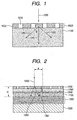
- Fig. 1 is a view for describing a photonic crystal layer applied to the present invention.
- a two-dimensional photonic crystal layer 1020 includes periodically provided pores 1010 and a region 1000 for isolating the pores 1010.
- a two-dimensional photonic crystal layer means a layer having a two-dimensional periodical change of the refractive index.
- a clad layer 1100 is adjacent to the photonic crystal layer 1020.
- Incident light 1030 which enters perpendicularly to the photonic crystal layer becomes transmitted light 1040 and diffracted light 1050.
- the diffracted light 1050 diffracted light which is obtained by diffraction at an angle ⁇ ( ⁇ is neither 0° nor 90°) of the incident light 1030 which enters the photonic crystal layer and has an oscillation wavelength ⁇ is used. Details of the photonic crystal layer for realizing such diffraction are described later.
- the transmitted light 1040 forms an angle of 0° with respect to the direction of incidence of the incident light 1030.
- Fig. 2 is a schematic sectional view for describing a surface emitting laser according to the present invention.
- a substrate 1500 has a multilayer mirror (DBR, Distributed Bragg Reflector) 1300 formed' thereon. Further, a lower clad layer 1105, an active layer 1200, an upper clad layer 1100, and a photonic crystal layer 1020 are formed on the multilayer mirror 1300. It is to be noted that the direction of lamination of the multilayer mirror 1300 is perpendicular to the substrate 1500.
- DBR Distributed Bragg Reflector
- the multilayer mirror 1300 is designed such that the reflectance of light which is perpendicularly incident.on.the mirror is the highest.
- thicknesses of the respective layers in the multilayer mirror are designed such that reflectance of light which is incident on the substrate at an angle ⁇ (set, for example, in a range of 20° to 80°) with respect to the perpendicular direction (corresponding to 1050 in Fig. 1 ) (second reflectance) is higher than reflectance of light which is perpendicularly incident on the substrate (first reflectance).
- the design is performed such that the second reflectance is 99 percent or more and 100 percent or less.
- the design is performed, more preferably, such that the second reflectance is 99.9 percent or more, and still more preferably, such that the second reflectance is 99.99 percent or more. The more the second reflectance approaches 100 percent, the more preferable it is.
- a distance d between an interface of the photonic crystal layer 1020 on a side of air and the multilayer mirror 1300 is designed as in the following.
- an optical path length which is a sum of an optical path 1051 of light incident on the multilayer mirror 1300 at the angle ⁇ and an optical path 1052 of light reflected by the multilayer mirror to return to a position that is away by a spacing 'a' between the pores is made to be an integer-fold length of the oscillation wavelength ⁇ .
- the oscillation wavelength ⁇ is determined.
- the spacing (lattice spacing) a between the pores in the photonic crystal formed in the form of a tetragonal lattice when the photonic crystal layer is viewed from a direction perpendicular to the substrate for a plan view thereof is determined.
- the lattice structure of the photonic crystal is not limited to a tetragonal lattice, and may be, for example, a triangular lattice structure.
- the design is performed such that when the light 1051 which is incident on the multilayer mirror from a position of a certain pore at the angle ⁇ is reflected by the mirror to return to a position that is away by the spacing a the phase matching condition is satisfied.
- n ⁇ a ⁇ sin ⁇ m ⁇
- n an effective refractive index of the clad layer 1100 in Fig. 2 .
- the effective refractive index n involves an influence of the active layer 1200 and the clad layer 1105 on the side of the substrate, which is required to be taken into consideration.
- ⁇ is determined when ⁇ and 'a' are determined. It is preferable that the range of ⁇ exceeds a critical angle of total reflection at an interface between the photonic crystal layer and air.
- d is geometrically determined.
- the optical path length which is the sum of the optical paths 1051 and 1052 is determined. Whether the optical path length satisfies the condition of an integer-fold of the oscillation wavelength (the phase matching condition) or not is confirmed. When the condition is not satisfied, 'a' is changed to perform the design such that the phase matching condition is satisfied.
- the thickness d is designed in terms of effective thickness taking into consideration the Goos-Haenchen shift and the refractive index of the photonic crystal layer.
- the diameter of the pores (when a section of a pore in the inplane direction of the substrate is a circle, such diameter means the diameter of the circle) is on the order of 40% of the lattice spacing.
- the diameter of the pores is designed to be in the range of 20% to 60% of the lattice spacing.
- the thickness of the photonic crystal layer is, for example, half of the lattice spacing a.
- phase matching condition is assumed to be satisfied when light returns to a position that is away from a certain pore by the spacing a
- the phase matching condition may be assumed to be satisfied at a portion that is away by an integer-fold of 'a', for example.
- the respective layers forming the multilayer mirror 1300 are designed as follows. That is, when the refractive index of each layer is n i , the thickness of the layer is set to ⁇ /(4 ⁇ n i ⁇ cos ⁇ i ).
- ⁇ i is an angle formed by an interface of each layer and the travel direction of light, but there are some cases where it can uniformly be defined as an incident angle from the clad layer 1105 to the multilayer mirror.
- the reflectance of each layer with regard to light incident on the multilayer mirror at the angle ⁇ with respect to the perpendicular direction can be made at the maximum or close to the maximum. More specifically, the reflectance of light which is incident on the mirror at an angle ⁇ can be made to be higher than the reflectance of light which is perpendicularly incident on the mirror. Further, because the reflectance of light incident on the multilayer mirror at an angle other than ⁇ (for example, an angle ⁇ ⁇ 20°) is lower than that of light incident at the angle ⁇ , confinement efficiency of other waveguide resonant modes when light is incident on the multilayer mirror at an angle other than ⁇ is lowered. As a result, multimode oscillation can be suppressed.
- Light incident on a lattice point of the photonic crystal layer from the side of the active layer maintains an angle formed by an axis perpendicular to the inplane direction of the substrate and the path of the incident light, and is diffracted to the side of the substrate in directions of the path of the incident light rotated by 0°, ⁇ 90°, and 180° with respect to the perpendicular axis.
- Light incident on the photonic crystal layer repeats the diffraction and the reflection at the multilayer reflector 1300 plural times and returns to the original incident light path, so resonance action is produced.
- light amplified in the resonator is diffracted from the photonic crystal layer in a direction perpendicular to the substrate, that is, diffracted in a similar manner to diffracted light 1060, to have a surface emitting function. Because the same phenomenon is produced at all the lattice points, coherent laser oscillation is possible over the whole area.
- the active layer one which emits light by carrier injection, one which emits light by an optical pump, or the like can be selected.
- a specific example is a multiple quantum well structure of a semiconductor.
- the structure is formed such that a resonant mode exists within the waveguide formed by the photonic crystal layer 1020 and the multilayer mirror 1300.
- the necessity to confine light within the photonic crystal layer is eliminated, so it is not indispensable to dispose a low refractive index medium at the interface of the photonic crystal layer on the side of the substrate.
- a low refractive index medium may be disposed at the interface of the photonic crystal layer on the side of the substrate.
- the present invention is characterized just in that it is not indispensable to dispose such a low refractive index medium.
- a reflector for example, a multilayer mirror
- a reflector other than the above-mentioned multilayer mirror having a reflectance with regard to the transmitted light which is higher than a reflectance with regard to the diffracted light may be provided between the substrate and the multilayer mirror. This enables reflection of light emitted to the side of the substrate to the side of the active layer, and the extraction efficiency of surface-emitted light to the side opposite to the substrate side can be enhanced.
- the photonic crystal layer which can be applied to the present invention is, for example, of a refractive index periodic structure where the refractive index periodically and two-dimensionally changes in the inplane direction.
- the structure may be a tetragonal lattice structure or a triangular lattice structure.
- a defect (a condition where the pore spacing is 'a' and a position that is away from a certain pore by 'a' does not have a pore which should be present there) may be introduced into the refractive index periodic structure. By introducing such a defect, the light extraction efficiency may be modulated at the defect.
- the lattice forming the photonic crystal layer is not necessarily required to be pores, and the pores may be filled with a material having a refractive index which is different from that of its surrounding, for example, a resin.
- the material of the photonic crystal layer may be, for example, a semiconductor, more specifically, Al 0.5 Ga 0.5 As or Al 0.6 Ga 0.4 N.
- the material of the multilayer mirror may be, for example, a semiconductor multilayer film, more specifically, Al 0.5 Ga 0.5 As/GaAs or Al 0.6 Ga 0.4 N/GaN.
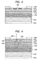
- a multilayer reflector 2300 including seventy pairs of an n-Al 0.93 Ga 0.07 As layer having a thickness of 59 nm and an n-Al 0.5 Ga 0.5 As layer having a thickness of 52 nm is grown on a GaAs substrate 2500.
- the growing method is, for example, MOCVD.
- the multilayer reflector is designed such that its reflectance with regard to light having a wavelength of 670 nm is maximimzed when the incident angle from the n-Al 0.93 Ga 0.07 As clad is about 24°.
- n-Al 0.93 Ga 0.07 As clad layer 2105, a GaInP/AlGaInP multiple quantum well layer 2200, a p-Al 0.93 Ga 0.07 As clad layer 2100, and a p-Al 0.5 Ga 0.5 As slab layer 2000 with which a resonator can be formed are grown on the multilayer reflector.
- a resist is applied to an upper surface of the slab layer 2000.
- two-dimensional tetragonal lattice circular patterns having a radius of 100 nm and a lattice spacing of 500 nm are formed on the resist.
- a lower electrode 2805 is formed under the substrate 2500 and an upper electrode 2800 is formed over the slab layer 2000.
- an active layer emits light, and by laser oscillation, laser light having a wavelength of 670 nm can be emitted in a direction perpendicular to the substrate.
- a second exemplary embodiment according to the present invention is characterized by including a second multilayer reflector 2350 between the substrate 2500 and the multilayer reflector.2300 (which is a first multilayer reflector) of the first exemplary embodiment as shown in the Fig. 4 which illustrates a main part thereof.
- the second multilayer reflector is characterized in that reflectance of light having a wavelength of laser oscillation which is perpendicularly incident on the reflector is higher than that of light which is obliquely incident.
- a second multilayer reflector 2350 including seventy pairs of an n-Al 0.93 Ga 0.07 As layer having a thickness of 54 nm and an n-Al 0.5 Ga 0.5 As layer having a thickness of 49 nm is grown on the substrate 2500, and the first multilayer reflector 2300 is formed thereon similarly to the case of the first exemplary embodiment.
- the reflectance of the second multilayer reflector with regard to light having a wavelength of 670 nm is maximized when the incident angle is a right angle.
- the second multilayer reflector has the function of returning to the side of an active layer 2200 light 2065 emitted from a laser resonator including the first multilayer reflector 2300, the photonic crystal layer 2020, and the active layer 2200 toward the side of the substrate in a direction perpendicular to the substrate.
- the surface emitting laser according to the present invention is not limited to the exemplary embodiments but various modifications can be made within the gist of the present invention.
- the materials of the semiconductor layer, the photonic crystal, the multilayer mirror, and the electrodes, the form of the lattice of the photonic crystal, the structure of the multilayer mirror, and the like may be appropriately set.
- the wavelength of laser oscillation is 670 nm
- the present invention is not limited thereto, and oscillation of an arbitrary wavelength is possible by selecting an appropriate material and an appropriate structure.
- the photonic crystal layer may be provided in the upper clad layer 1100, the active layer 1200, the lower clad layer 1105, or the multilayer mirror 1300.
- the refractive index periodic structure may be provided in such plural layers.
Landscapes
- Physics & Mathematics (AREA)
- Optics & Photonics (AREA)
- Condensed Matter Physics & Semiconductors (AREA)
- General Physics & Mathematics (AREA)
- Electromagnetism (AREA)
- Engineering & Computer Science (AREA)
- Nanotechnology (AREA)
- Chemical & Material Sciences (AREA)
- Biophysics (AREA)
- Crystallography & Structural Chemistry (AREA)
- Life Sciences & Earth Sciences (AREA)
- Semiconductor Lasers (AREA)
- Optical Integrated Circuits (AREA)
Applications Claiming Priority (2)
| Application Number | Priority Date | Filing Date | Title |
|---|---|---|---|
| JP2006109913A JP4533339B2 (ja) | 2006-04-12 | 2006-04-12 | 面発光レーザ |
| PCT/JP2007/058018 WO2007119761A2 (en) | 2006-04-12 | 2007-04-05 | Vcsel with photonic crystal mirror for waveguiding by diffraction |
Publications (2)
| Publication Number | Publication Date |
|---|---|
| EP2011206A2 EP2011206A2 (en) | 2009-01-07 |
| EP2011206B1 true EP2011206B1 (en) | 2011-06-15 |
Family
ID=38609910
Family Applications (1)
| Application Number | Title | Priority Date | Filing Date |
|---|---|---|---|
| EP07741454A Not-in-force EP2011206B1 (en) | 2006-04-12 | 2007-04-05 | Vcsel with photonic crystal mirror for waveguiding by diffraction |
Country Status (7)
Families Citing this family (15)
| Publication number | Priority date | Publication date | Assignee | Title |
|---|---|---|---|---|
| JP4709259B2 (ja) * | 2007-10-12 | 2011-06-22 | キヤノン株式会社 | 面発光レーザ |
| JP5171318B2 (ja) * | 2008-03-05 | 2013-03-27 | キヤノン株式会社 | 面発光レーザアレイ |
| JP4968959B2 (ja) * | 2008-03-06 | 2012-07-04 | キヤノン株式会社 | フォトニック結晶および該フォトニック結晶を用いた面発光レーザ |
| JP5388666B2 (ja) * | 2008-04-21 | 2014-01-15 | キヤノン株式会社 | 面発光レーザ |
| JP4639249B2 (ja) | 2008-07-31 | 2011-02-23 | キヤノン株式会社 | 面発光レーザの製造方法及び面発光レーザアレイの製造方法、面発光レーザ及び面発光レーザアレイ、面発光レーザアレイを備えている光学機器 |
| JP5106487B2 (ja) * | 2008-07-31 | 2012-12-26 | キヤノン株式会社 | 面発光レーザの製造方法及び面発光レーザアレイの製造方法、該製造方法による面発光レーザアレイを備えている光学機器 |
| JP5038371B2 (ja) * | 2008-09-26 | 2012-10-03 | キヤノン株式会社 | 面発光レーザの製造方法 |
| JP5183555B2 (ja) * | 2009-04-02 | 2013-04-17 | キヤノン株式会社 | 面発光レーザアレイ |
| JP5312159B2 (ja) * | 2009-04-08 | 2013-10-09 | キヤノン株式会社 | 3次元フォトニック結晶の製造方法および光機能素子、発光素子 |
| CN101655885B (zh) * | 2009-08-27 | 2012-01-11 | 南京理工大学 | 一种高效率二维光子晶体偏轴定向发射器的设计方法 |
| US9042421B2 (en) | 2010-10-18 | 2015-05-26 | Canon Kabushiki Kaisha | Surface emitting laser, surface emitting laser array, and optical apparatus having surface emitting laser array |
| KR101799521B1 (ko) | 2011-05-24 | 2017-11-20 | 삼성전자 주식회사 | 광결정형 광변조기 및 이를 구비하는 3차원 영상 획득 장치 |
| KR101928436B1 (ko) | 2012-10-10 | 2019-02-26 | 삼성전자주식회사 | 광 집적 회로용 하이브리드 수직 공명 레이저 |
| CN104380760B (zh) * | 2013-02-20 | 2019-03-26 | 松下电器(美国)知识产权公司 | 便携信息终端及其控制方法 |
| JP7378686B2 (ja) * | 2021-08-31 | 2023-11-13 | シチズン電子株式会社 | Led発光装置 |
Family Cites Families (12)
| Publication number | Priority date | Publication date | Assignee | Title |
|---|---|---|---|---|
| US5231642A (en) * | 1992-05-08 | 1993-07-27 | Spectra Diode Laboratories, Inc. | Semiconductor ring and folded cavity lasers |
| US6603605B1 (en) * | 1999-11-05 | 2003-08-05 | Interuniversitair Microelektronica Centrum (Imec, Vzw) | System for guiding a beam of electromagnetic radiation |
| US7031360B2 (en) * | 2002-02-12 | 2006-04-18 | Nl Nanosemiconductor Gmbh | Tilted cavity semiconductor laser (TCSL) and method of making same |
| JP2003273456A (ja) * | 2002-03-14 | 2003-09-26 | Japan Science & Technology Corp | 2次元フォトニック結晶面発光レーザ |
| US6704343B2 (en) * | 2002-07-18 | 2004-03-09 | Finisar Corporation | High power single mode vertical cavity surface emitting laser |
| TW200524236A (en) | 2003-12-01 | 2005-07-16 | Nl Nanosemiconductor Gmbh | Optoelectronic device incorporating an interference filter |
| JP4820749B2 (ja) * | 2004-03-05 | 2011-11-24 | 国立大学法人京都大学 | 2次元フォトニック結晶面発光レーザ光源 |
| JP4116587B2 (ja) * | 2004-04-13 | 2008-07-09 | 浜松ホトニクス株式会社 | 半導体発光素子及びその製造方法 |
| US7689086B2 (en) * | 2004-07-30 | 2010-03-30 | University Of Connecticut | Resonant leaky-mode optical devices and associated methods |
| US7697588B2 (en) | 2006-11-02 | 2010-04-13 | Canon Kabushiki Kaisha | Structure having photonic crystal and surface-emitting laser using the same |
| US7499481B2 (en) | 2006-11-14 | 2009-03-03 | Canon Kabushiki Kaisha | Surface-emitting laser and method for producing the same |
| US7535946B2 (en) * | 2006-11-16 | 2009-05-19 | Canon Kabushiki Kaisha | Structure using photonic crystal and surface emitting laser |
-
2006
- 2006-04-12 JP JP2006109913A patent/JP4533339B2/ja not_active Expired - Fee Related
-
2007
- 2007-04-05 CN CN2007800130535A patent/CN101421889B/zh not_active Expired - Fee Related
- 2007-04-05 KR KR1020087027310A patent/KR100991068B1/ko not_active Expired - Fee Related
- 2007-04-05 US US11/916,230 patent/US7796665B2/en not_active Expired - Fee Related
- 2007-04-05 EP EP07741454A patent/EP2011206B1/en not_active Not-in-force
- 2007-04-05 WO PCT/JP2007/058018 patent/WO2007119761A2/en active Application Filing
- 2007-04-05 AT AT07741454T patent/ATE513344T1/de not_active IP Right Cessation
-
2010
- 2010-08-10 US US12/853,393 patent/US8249123B2/en not_active Expired - Fee Related
Also Published As
| Publication number | Publication date |
|---|---|
| US20100303117A1 (en) | 2010-12-02 |
| CN101421889A (zh) | 2009-04-29 |
| KR100991068B1 (ko) | 2010-10-29 |
| EP2011206A2 (en) | 2009-01-07 |
| WO2007119761A2 (en) | 2007-10-25 |
| US20100014548A1 (en) | 2010-01-21 |
| JP2007287733A (ja) | 2007-11-01 |
| WO2007119761B1 (en) | 2008-05-22 |
| WO2007119761A3 (en) | 2008-04-03 |
| KR20090015920A (ko) | 2009-02-12 |
| US8249123B2 (en) | 2012-08-21 |
| JP4533339B2 (ja) | 2010-09-01 |
| CN101421889B (zh) | 2011-01-19 |
| US7796665B2 (en) | 2010-09-14 |
| ATE513344T1 (de) | 2011-07-15 |
Similar Documents
| Publication | Publication Date | Title |
|---|---|---|
| EP2011206B1 (en) | Vcsel with photonic crystal mirror for waveguiding by diffraction | |
| JP4709259B2 (ja) | 面発光レーザ | |
| US7795058B2 (en) | Method for manufacturing optical element | |
| US7483466B2 (en) | Vertical cavity surface emitting laser device | |
| US7535946B2 (en) | Structure using photonic crystal and surface emitting laser | |
| JP4027392B2 (ja) | 垂直共振器型面発光レーザ装置 | |
| US7733936B2 (en) | Surface emitting laser | |
| Sciancalepore et al. | CMOS-compatible ultra-compact 1.55-μ m emitting VCSELs using double photonic crystal mirrors | |
| JP4927411B2 (ja) | 2次元フォトニック結晶面発光レーザ | |
| JP5356088B2 (ja) | 半導体レーザ、レーザ光の発生方法、およびレーザ光のスペクトル線幅の狭窄化方法 | |
| JP2624279B2 (ja) | スラブ導波光出射半導体レーザー | |
| JP2004119671A (ja) | 光アクティブデバイス | |
| JPWO2010116460A1 (ja) | 光素子及びその製造方法 | |
| JP4906704B2 (ja) | 面発光レーザ、及び面発光レーザを備えた発光装置 | |
| JP2008098379A (ja) | 2次元フォトニック結晶面発光レーザおよびその製造方法 | |
| US10243330B2 (en) | Optoelectronic device with resonant suppression of high order optical modes and method of making same | |
| KR100576299B1 (ko) | 반도체 레이저 및 광통신용 소자 | |
| JP4300246B2 (ja) | フォトニック結晶を有する構造体及びそれを用いた面発光レーザ | |
| Shchukin et al. | Modeling of photonic-crystal-based high-power high-brightness semiconductor lasers | |
| JP2010129955A (ja) | 分布帰還型半導体レーザ | |
| JPH09148679A (ja) | 半導体発光素子 |
Legal Events
| Date | Code | Title | Description |
|---|---|---|---|
| PUAI | Public reference made under article 153(3) epc to a published international application that has entered the european phase |
Free format text: ORIGINAL CODE: 0009012 |
|
| 17P | Request for examination filed |
Effective date: 20081112 |
|
| AK | Designated contracting states |
Kind code of ref document: A2 Designated state(s): AT BE BG CH CY CZ DE DK EE ES FI FR GB GR HU IE IS IT LI LT LU LV MC MT NL PL PT RO SE SI SK TR |
|
| AX | Request for extension of the european patent |
Extension state: AL BA HR MK RS |
|
| 17Q | First examination report despatched |
Effective date: 20090127 |
|
| GRAP | Despatch of communication of intention to grant a patent |
Free format text: ORIGINAL CODE: EPIDOSNIGR1 |
|
| DAX | Request for extension of the european patent (deleted) | ||
| GRAS | Grant fee paid |
Free format text: ORIGINAL CODE: EPIDOSNIGR3 |
|
| GRAA | (expected) grant |
Free format text: ORIGINAL CODE: 0009210 |
|
| AK | Designated contracting states |
Kind code of ref document: B1 Designated state(s): AT BE BG CH CY CZ DE DK EE ES FI FR GB GR HU IE IS IT LI LT LU LV MC MT NL PL PT RO SE SI SK TR |
|
| REG | Reference to a national code |
Ref country code: GB Ref legal event code: FG4D Ref country code: CH Ref legal event code: EP |
|
| REG | Reference to a national code |
Ref country code: IE Ref legal event code: FG4D |
|
| REG | Reference to a national code |
Ref country code: DE Ref legal event code: R096 Ref document number: 602007015241 Country of ref document: DE Effective date: 20110721 |
|
| REG | Reference to a national code |
Ref country code: NL Ref legal event code: VDEP Effective date: 20110615 |
|
| PG25 | Lapsed in a contracting state [announced via postgrant information from national office to epo] |
Ref country code: SE Free format text: LAPSE BECAUSE OF FAILURE TO SUBMIT A TRANSLATION OF THE DESCRIPTION OR TO PAY THE FEE WITHIN THE PRESCRIBED TIME-LIMIT Effective date: 20110615 Ref country code: LT Free format text: LAPSE BECAUSE OF FAILURE TO SUBMIT A TRANSLATION OF THE DESCRIPTION OR TO PAY THE FEE WITHIN THE PRESCRIBED TIME-LIMIT Effective date: 20110615 |
|
| PG25 | Lapsed in a contracting state [announced via postgrant information from national office to epo] |
Ref country code: FI Free format text: LAPSE BECAUSE OF FAILURE TO SUBMIT A TRANSLATION OF THE DESCRIPTION OR TO PAY THE FEE WITHIN THE PRESCRIBED TIME-LIMIT Effective date: 20110615 Ref country code: SI Free format text: LAPSE BECAUSE OF FAILURE TO SUBMIT A TRANSLATION OF THE DESCRIPTION OR TO PAY THE FEE WITHIN THE PRESCRIBED TIME-LIMIT Effective date: 20110615 Ref country code: CY Free format text: LAPSE BECAUSE OF FAILURE TO SUBMIT A TRANSLATION OF THE DESCRIPTION OR TO PAY THE FEE WITHIN THE PRESCRIBED TIME-LIMIT Effective date: 20110615 Ref country code: AT Free format text: LAPSE BECAUSE OF FAILURE TO SUBMIT A TRANSLATION OF THE DESCRIPTION OR TO PAY THE FEE WITHIN THE PRESCRIBED TIME-LIMIT Effective date: 20110615 Ref country code: GR Free format text: LAPSE BECAUSE OF FAILURE TO SUBMIT A TRANSLATION OF THE DESCRIPTION OR TO PAY THE FEE WITHIN THE PRESCRIBED TIME-LIMIT Effective date: 20110916 Ref country code: LV Free format text: LAPSE BECAUSE OF FAILURE TO SUBMIT A TRANSLATION OF THE DESCRIPTION OR TO PAY THE FEE WITHIN THE PRESCRIBED TIME-LIMIT Effective date: 20110615 |
|
| PG25 | Lapsed in a contracting state [announced via postgrant information from national office to epo] |
Ref country code: BE Free format text: LAPSE BECAUSE OF FAILURE TO SUBMIT A TRANSLATION OF THE DESCRIPTION OR TO PAY THE FEE WITHIN THE PRESCRIBED TIME-LIMIT Effective date: 20110615 Ref country code: NL Free format text: LAPSE BECAUSE OF FAILURE TO SUBMIT A TRANSLATION OF THE DESCRIPTION OR TO PAY THE FEE WITHIN THE PRESCRIBED TIME-LIMIT Effective date: 20110615 |
|
| PG25 | Lapsed in a contracting state [announced via postgrant information from national office to epo] |
Ref country code: PT Free format text: LAPSE BECAUSE OF FAILURE TO SUBMIT A TRANSLATION OF THE DESCRIPTION OR TO PAY THE FEE WITHIN THE PRESCRIBED TIME-LIMIT Effective date: 20111017 Ref country code: CZ Free format text: LAPSE BECAUSE OF FAILURE TO SUBMIT A TRANSLATION OF THE DESCRIPTION OR TO PAY THE FEE WITHIN THE PRESCRIBED TIME-LIMIT Effective date: 20110615 Ref country code: IS Free format text: LAPSE BECAUSE OF FAILURE TO SUBMIT A TRANSLATION OF THE DESCRIPTION OR TO PAY THE FEE WITHIN THE PRESCRIBED TIME-LIMIT Effective date: 20111015 Ref country code: EE Free format text: LAPSE BECAUSE OF FAILURE TO SUBMIT A TRANSLATION OF THE DESCRIPTION OR TO PAY THE FEE WITHIN THE PRESCRIBED TIME-LIMIT Effective date: 20110615 |
|
| PG25 | Lapsed in a contracting state [announced via postgrant information from national office to epo] |
Ref country code: SK Free format text: LAPSE BECAUSE OF FAILURE TO SUBMIT A TRANSLATION OF THE DESCRIPTION OR TO PAY THE FEE WITHIN THE PRESCRIBED TIME-LIMIT Effective date: 20110615 Ref country code: RO Free format text: LAPSE BECAUSE OF FAILURE TO SUBMIT A TRANSLATION OF THE DESCRIPTION OR TO PAY THE FEE WITHIN THE PRESCRIBED TIME-LIMIT Effective date: 20110615 Ref country code: PL Free format text: LAPSE BECAUSE OF FAILURE TO SUBMIT A TRANSLATION OF THE DESCRIPTION OR TO PAY THE FEE WITHIN THE PRESCRIBED TIME-LIMIT Effective date: 20110615 |
|
| PLBE | No opposition filed within time limit |
Free format text: ORIGINAL CODE: 0009261 |
|
| STAA | Information on the status of an ep patent application or granted ep patent |
Free format text: STATUS: NO OPPOSITION FILED WITHIN TIME LIMIT |
|
| 26N | No opposition filed |
Effective date: 20120316 |
|
| PG25 | Lapsed in a contracting state [announced via postgrant information from national office to epo] |
Ref country code: IT Free format text: LAPSE BECAUSE OF FAILURE TO SUBMIT A TRANSLATION OF THE DESCRIPTION OR TO PAY THE FEE WITHIN THE PRESCRIBED TIME-LIMIT Effective date: 20110615 |
|
| PG25 | Lapsed in a contracting state [announced via postgrant information from national office to epo] |
Ref country code: DK Free format text: LAPSE BECAUSE OF FAILURE TO SUBMIT A TRANSLATION OF THE DESCRIPTION OR TO PAY THE FEE WITHIN THE PRESCRIBED TIME-LIMIT Effective date: 20110615 |
|
| REG | Reference to a national code |
Ref country code: DE Ref legal event code: R097 Ref document number: 602007015241 Country of ref document: DE Effective date: 20120316 |
|
| PG25 | Lapsed in a contracting state [announced via postgrant information from national office to epo] |
Ref country code: MC Free format text: LAPSE BECAUSE OF NON-PAYMENT OF DUE FEES Effective date: 20120430 |
|
| REG | Reference to a national code |
Ref country code: CH Ref legal event code: PL |
|
| REG | Reference to a national code |
Ref country code: IE Ref legal event code: MM4A |
|
| REG | Reference to a national code |
Ref country code: FR Ref legal event code: ST Effective date: 20121228 |
|
| PG25 | Lapsed in a contracting state [announced via postgrant information from national office to epo] |
Ref country code: LI Free format text: LAPSE BECAUSE OF NON-PAYMENT OF DUE FEES Effective date: 20120430 Ref country code: CH Free format text: LAPSE BECAUSE OF NON-PAYMENT OF DUE FEES Effective date: 20120430 Ref country code: IE Free format text: LAPSE BECAUSE OF NON-PAYMENT OF DUE FEES Effective date: 20120405 |
|
| PG25 | Lapsed in a contracting state [announced via postgrant information from national office to epo] |
Ref country code: FR Free format text: LAPSE BECAUSE OF NON-PAYMENT OF DUE FEES Effective date: 20120430 |
|
| PG25 | Lapsed in a contracting state [announced via postgrant information from national office to epo] |
Ref country code: ES Free format text: LAPSE BECAUSE OF FAILURE TO SUBMIT A TRANSLATION OF THE DESCRIPTION OR TO PAY THE FEE WITHIN THE PRESCRIBED TIME-LIMIT Effective date: 20110926 |
|
| PG25 | Lapsed in a contracting state [announced via postgrant information from national office to epo] |
Ref country code: BG Free format text: LAPSE BECAUSE OF FAILURE TO SUBMIT A TRANSLATION OF THE DESCRIPTION OR TO PAY THE FEE WITHIN THE PRESCRIBED TIME-LIMIT Effective date: 20110915 |
|
| PG25 | Lapsed in a contracting state [announced via postgrant information from national office to epo] |
Ref country code: MT Free format text: LAPSE BECAUSE OF FAILURE TO SUBMIT A TRANSLATION OF THE DESCRIPTION OR TO PAY THE FEE WITHIN THE PRESCRIBED TIME-LIMIT Effective date: 20110615 |
|
| PG25 | Lapsed in a contracting state [announced via postgrant information from national office to epo] |
Ref country code: TR Free format text: LAPSE BECAUSE OF FAILURE TO SUBMIT A TRANSLATION OF THE DESCRIPTION OR TO PAY THE FEE WITHIN THE PRESCRIBED TIME-LIMIT Effective date: 20110615 |
|
| PG25 | Lapsed in a contracting state [announced via postgrant information from national office to epo] |
Ref country code: LU Free format text: LAPSE BECAUSE OF NON-PAYMENT OF DUE FEES Effective date: 20120405 |
|
| PG25 | Lapsed in a contracting state [announced via postgrant information from national office to epo] |
Ref country code: HU Free format text: LAPSE BECAUSE OF FAILURE TO SUBMIT A TRANSLATION OF THE DESCRIPTION OR TO PAY THE FEE WITHIN THE PRESCRIBED TIME-LIMIT Effective date: 20070405 |
|
| PGFP | Annual fee paid to national office [announced via postgrant information from national office to epo] |
Ref country code: GB Payment date: 20160427 Year of fee payment: 10 Ref country code: DE Payment date: 20160430 Year of fee payment: 10 |
|
| REG | Reference to a national code |
Ref country code: DE Ref legal event code: R119 Ref document number: 602007015241 Country of ref document: DE |
|
| GBPC | Gb: european patent ceased through non-payment of renewal fee |
Effective date: 20170405 |
|
| PG25 | Lapsed in a contracting state [announced via postgrant information from national office to epo] |
Ref country code: DE Free format text: LAPSE BECAUSE OF NON-PAYMENT OF DUE FEES Effective date: 20171103 |
|
| PG25 | Lapsed in a contracting state [announced via postgrant information from national office to epo] |
Ref country code: GB Free format text: LAPSE BECAUSE OF NON-PAYMENT OF DUE FEES Effective date: 20170405 |