EP2000567A2 - Verfahren zur züchtung von iii-nitrid-einzelkristallen - Google Patents
Verfahren zur züchtung von iii-nitrid-einzelkristallen Download PDFInfo
- Publication number
- EP2000567A2 EP2000567A2 EP07739311A EP07739311A EP2000567A2 EP 2000567 A2 EP2000567 A2 EP 2000567A2 EP 07739311 A EP07739311 A EP 07739311A EP 07739311 A EP07739311 A EP 07739311A EP 2000567 A2 EP2000567 A2 EP 2000567A2
- Authority
- EP
- European Patent Office
- Prior art keywords
- single crystal
- source material
- source
- impurity element
- crucible
- Prior art date
- Legal status (The legal status is an assumption and is not a legal conclusion. Google has not performed a legal analysis and makes no representation as to the accuracy of the status listed.)
- Granted
Links
Images


Classifications
-
- C—CHEMISTRY; METALLURGY
- C30—CRYSTAL GROWTH
- C30B—SINGLE-CRYSTAL GROWTH; UNIDIRECTIONAL SOLIDIFICATION OF EUTECTIC MATERIAL OR UNIDIRECTIONAL DEMIXING OF EUTECTOID MATERIAL; REFINING BY ZONE-MELTING OF MATERIAL; PRODUCTION OF A HOMOGENEOUS POLYCRYSTALLINE MATERIAL WITH DEFINED STRUCTURE; SINGLE CRYSTALS OR HOMOGENEOUS POLYCRYSTALLINE MATERIAL WITH DEFINED STRUCTURE; AFTER-TREATMENT OF SINGLE CRYSTALS OR A HOMOGENEOUS POLYCRYSTALLINE MATERIAL WITH DEFINED STRUCTURE; APPARATUS THEREFOR
- C30B29/00—Single crystals or homogeneous polycrystalline material with defined structure characterised by the material or by their shape
- C30B29/10—Inorganic compounds or compositions
- C30B29/40—AIIIBV compounds wherein A is B, Al, Ga, In or Tl and B is N, P, As, Sb or Bi
- C30B29/403—AIII-nitrides
-
- C—CHEMISTRY; METALLURGY
- C30—CRYSTAL GROWTH
- C30B—SINGLE-CRYSTAL GROWTH; UNIDIRECTIONAL SOLIDIFICATION OF EUTECTIC MATERIAL OR UNIDIRECTIONAL DEMIXING OF EUTECTOID MATERIAL; REFINING BY ZONE-MELTING OF MATERIAL; PRODUCTION OF A HOMOGENEOUS POLYCRYSTALLINE MATERIAL WITH DEFINED STRUCTURE; SINGLE CRYSTALS OR HOMOGENEOUS POLYCRYSTALLINE MATERIAL WITH DEFINED STRUCTURE; AFTER-TREATMENT OF SINGLE CRYSTALS OR A HOMOGENEOUS POLYCRYSTALLINE MATERIAL WITH DEFINED STRUCTURE; APPARATUS THEREFOR
- C30B23/00—Single-crystal growth by condensing evaporated or sublimed materials
-
- C—CHEMISTRY; METALLURGY
- C30—CRYSTAL GROWTH
- C30B—SINGLE-CRYSTAL GROWTH; UNIDIRECTIONAL SOLIDIFICATION OF EUTECTIC MATERIAL OR UNIDIRECTIONAL DEMIXING OF EUTECTOID MATERIAL; REFINING BY ZONE-MELTING OF MATERIAL; PRODUCTION OF A HOMOGENEOUS POLYCRYSTALLINE MATERIAL WITH DEFINED STRUCTURE; SINGLE CRYSTALS OR HOMOGENEOUS POLYCRYSTALLINE MATERIAL WITH DEFINED STRUCTURE; AFTER-TREATMENT OF SINGLE CRYSTALS OR A HOMOGENEOUS POLYCRYSTALLINE MATERIAL WITH DEFINED STRUCTURE; APPARATUS THEREFOR
- C30B29/00—Single crystals or homogeneous polycrystalline material with defined structure characterised by the material or by their shape
- C30B29/10—Inorganic compounds or compositions
- C30B29/38—Nitrides
Definitions
- the present invention relates to methods of growing Group III nitride single crystals utilized in substrates for light-emitting diodes, electronic devices, semiconductor sensors, and other semiconductor devices.
- the invention relates to a method of growing low-dislocation-density III-nitride single crystals of favorable crystallinity.
- III-nitride crystals such as Al x Ga 1- x N (0 ⁇ x ⁇ 1, likewise hereinafter) single crystals are extraordinarily useful as materials for building semiconductor devices such as light-emitting diodes, electronic devices, and semiconductor sensors.
- III-nitride single crystals examples include vapor-phase techniques, particularly among which sublimation has been singled out from the perspective of obtaining crystals of satisfactory crystallinity with a narrow full-width at half-maximum for the X-ray diffraction peak.
- Patent Document 1 the specifications for U.S. Pat. No. 5,858,086
- Patent Document 2 U.S. Pat. No. 6,296,956
- Patent Document 3 U.S. Pat. No. 6,001,748
- Patent Document 1 U.S. Pat. No. 5,858,086 specification
- Patent Document 2 U.S. Pat. No. 6,296,956 specification
- Patent Document 3 U.S. Pat. No. 6, 001, 748 specification
- An object of the present invention is to make available a method of stably growing bulk III-nitride single crystal of low dislocation density and favorable crystallinity.
- the present invention is a III-nitride single-crystal growth method furnished with a step of placing source material in a crucible, and a step of sublimating the source material to grow an Al x Ga 1- x N (0 ⁇ x ⁇ 1) single crystal in the crucible, wherein the source material includes an Al y Ga 1- y N (0 ⁇ y ⁇ 1) source and an impurity element, which is at least one selected from the group consisting of Group IVb elements and Group IIa elements.
- a first source material compartment, a second source material compartment, and a crystal-growth compartment are provided in the crucible, with openings for ventilation being provided between the first and the second source material compartments and between at least one of them and the crystal-growth compartment, and the Al y Ga 1- y N source material can be arranged in the first source material compartment, and the impurity element in the second source material compartment.
- the source material may be a mixture of the Al y Ga 1- y N source and the impurity element.
- the impurity element any one of Si, C, and Ge can be utilized.
- a ratio n E / n A of the number of moles n E of the impurity element atoms to the number of moles n A of the Al atoms in the Al y Ga 1- y N source can be made 0.01 to 0.5 inclusive.
- a ratio n E / n o of the number of moles n E of the impurity element atoms to the number of moles no of atoms of the oxygen contained in the source material can be made 2 to 1 ⁇ 10 4 inclusive.
- the crucible can be formed from metal carbide.
- an undersubstrate can be arranged in the crucible to grow Al x Ga 1- x N single crystal on the undersubstrate.
- the Al x Ga 1- x N single crystal diameter can be brought to a span of more than 2 inches.
- the III-nitride single crystal growth method can be further furnished with a step of sublimating an Al t Ga 1- t N (0 ⁇ t ⁇ 1) source to grow onto the Al x Ga 1- x N single crystal monocrystalline Al s Ga 1- s N (0 ⁇ S ⁇ 1) with a lower impurity-element concentration by comparison to that of the Al x Ga 1- x N single crystal.
- the present invention affords a method of stably growing bulk III-nitride single crystals of low dislocation density and of favorable crystallinity.
- 1 source material
- 2 Al y Ga 1- y N source
- 3 impurity element
- 4 Al x Ga 1- x N single crystal
- 5 Al s Ga 1- s N single crystal
- 7 Al t Ga 1- t N source
- 9 undersubstrate
- 10 sublimation furnace
- 11 reaction chamber
- 11 a N 2 gas inlet
- 11 b N 2 gas outlet
- 12 crucible
- 12 a , 12 b , 12 c , and 12e ventilation openings
- 12 p first source material compartment
- 12 q second source material compartment
- 12 r crystal-growth compartment
- 13 heater
- 14 high-frequency heating coils
- 15 radiation thermometers
- 16 undersubstrate protector.
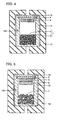
- One embodiment mode of the III-nitride single crystal growth method involving the present invention is characterized in being furnished with a step of , referring to Fig. 1 , placing source material 1 in a crucible 12, and a step of sublimating the source material 1 to grow an Al x Ga 1- x N (0 ⁇ x ⁇ 1, hereinafter) single crystal 4 in the crucible 12, and characterized in that the source material 1 is composed of Al y Ga 1- y N (0 ⁇ y ⁇ 1, hereinafter) source 2 and impurity element 3, and the impurity element is at least a single kind element selected from the group consisting of IVb elements and IIa elements.
- the Al y Ga 1- y N source 2 that is a direct source material for forming the Al x Ga 1- x N single crystal 4, together with at least a single kind of impurity element 3 selected from the group consisting of IVb elements and IIa elements, the rate at which the Al x Ga 1- x N single crystal 4 grows heightens, to grow bulk Al x Ga 1- x N single crystal 4 of low dislocation density and favorable crystallinity stably.
- Such an impurity element E is believed to react with Al to become Al p E q (g) (herein, p and q are positive numbers), and to act as material for transporting Al during growth of the Al x Ga 1- x N single crystal 4, heightening the crystal growth rate, as well as reducing dislocation densities to enhance crystallinity.
- the source material 1 includes the Al y Ga 1- y N source material 2 and at least a single kind of impurity element 3 selected from the group consisting of IVb elements and IIa elements, and the manner in which they are included in the source material is not limited. Therefore, the Al y Ga 1- y N source 2 collectively and the impurity element 3 collectively may be each arranged in the crucible 12, as illustrated in Fig. 1 . Also as illustrated in Fig.2 , the Al y Ga 1- y N source 2 and impurity element 3 may be arranged mixed together in the crucible 12. Furthermore, as illustrated in Fig.
- the Al y Ga 1- y N source material 2 may be arranged in the first source material compartment 12 p , and the impurity element 3 in the second source material compartment 12 q .
- the Al y Ga 1- y N source material 2 and impurity element 3 have is not particularly limited as long as the Al y Ga 1- y N source material 2 and impurity element 3 are in the form that enables controlling their relative proportions-that is, if in solid form, they may be block-like, granular, and powdery. It should be understood that in the situation in which the crucible 12, and the source material compartments 12 p , 12 q and crystal-growth compartment 12 r that will be explained hereinafter are formed of the impurity element 3, the concentration of the impurity element 3 cannot be controlled, which prevents above impurity element effect from being brought during Al x Ga 1- x N single crystal growth.
- the sublimation method utilized in this embodiment means the method in which, referring to Fig. 1 , the source material 1 including the Al y Ga 1- y N source 2 is sublimated, and then is solidified again to produce the Al x Ga 1- x N single crystal 4.
- a vertical high-frequency-heating sublimation furnace 10 as illustrated in Fig. 1 is employed, for example.
- the WC crucible 12 having a ventilation opening 12e is disposed in the center part of a reaction chamber 11 in the vertical sublimation furnace 10, with a heater 13 being provided around the crucible 12 so that ventilation from the inside of, to the outside of, the crucible 12 is secured.
- high-frequency heating coils 14 for heating the heater 13 are disposed centrally along the outer side of the reaction chamber 11. Additionally, an N 2 gas inlet 11 a for passing N 2 gas into the reaction chamber 11 outside of the crucible 12, an outlet 11 c , and radiation thermometers 15 for measuring the temperatures of the bottom and top sides of the crucible 12 are provided to the ends of the reaction chamber 11.
- the Al x Ga 1- x N single crystal 4 can be manufactured employing above vertical sublimation furnace 10.
- the source material 1 including the Al y Ga 1- y N source 2 and impurity element 3 are housed in the lower part of the crucible 12, and with the N 2 gas being continuously passed into the reaction chamber 11, the temperature in the crucible 12 is raised by heating the heater 13 employing the high-frequency heating coils 14, and the temperature of the part in the crucible 12 where the source material 1 is housed is kept higher than that of the rest in the crucible 12, to sublimate the Al x Ga 1- x N and impurity element in the source material 1, and then the Al x Ga 1- x N is solidified again in the upper part of the crucible 12 to grow the Al x Ga 1- x N single crystal 4.
- the Al x Ga 1- x N single crystal 4 As a result of, during the growth of the Al x Ga 1- x N single crystal 4, bringing the temperature of the part in the crucible 12 where the source material 1 is housed to a level of 1600°C to 2300°C, and making the temperature of the upper part in the crucible 12 (where the Al x Ga 1- x N single crystal 4 is grown) approximately 10°C to 200°C lower than that of the part in the crucible 12 where the source material 1 is housed, the Al x Ga 1- x N single crystal 4 of favorable crystallinity can be obtained. Moreover, passing N 2 gas into the reaction chamber 11 outside the crucible 12 continuously also during crystal growth reduces the mixing of the impurities into the Al x Ga 1- x N single crystal 4.
- impurity element is at least a single kind element selected from the group consisting of IVb elements and IIa elements.
- the IVb and IIa elements which are believed to act as materials for transporting Al, heightens Al x Ga 1- x N single crystal growth rate and enhances crystallinity.
- Group IVb elements mean elements categorized into Group IVb in periodic table of the elements, and C (carbon), Si (silicon), and Ge (germanium) fall into the Group IVb.
- Group IIa elements which are called also alkaline earth metal, mean elements categorized into Group IIa in periodic table of the elements, and Mg (magnesium) and Ca (calcium) fall into the Group IIa.
- a plurality of impurity elements selected from above IVb and IIa elements can be used at the same time. Selecting a plurality of elements (for example, Si and C) from IVb elements is less than optimal, however, because the selected plurality of elements (Si and C) react with each other to form a stable compound (SiC), and thus lose the effect of acting as materials for transporting Al, sometimes resulting in failure to offer advantages sufficient to heighten Al x Ga 1- x N single crystal growth and to enhance crystallinity.
- the impurity element is preferably any one of Ai, C, and Ge.
- any one specific element picked out from IVb elements-particularly, Si, C, or Ge among them- is preferable from the perspective of heightening Al x Ga 1- x N single crystal growth rate and of enhancing crystallinity.
- ratio n E / n A (simply, molar ratio n E / n A , hereinafter) of the number of moles n E of the atoms of the impurity element 3 to the number of moles n A of the Al atoms in the Al y Ga 1- y N source 2 is preferably between 0.01 and 0.5 inclusive, and more preferably, is between 0.05 and 0.5 inclusive.
- the impurity element has an attenuated effect of acting as material for transporting Al, and at a molar ratio n E / n A of more than 0.5, growth of the Al x Ga 1- x N single crystal 4 is blocked.
- ratio n E / n O (simply, molar ratio n E / n O , hereinafter) of the number of moles n E of the atoms of the impurity element 3 to the number of moles n O of the atoms of oxygen contained in the source material 1 is preferably between 2 and 1 ⁇ 10 4 inclusive.
- the molar ratio n E / n O is preferably between 3 and 1 ⁇ 10 4 inclusive, and more preferably, is between 10 and 1 ⁇ 10 4 inclusive.
- the number of moles of the atoms of oxygen contained in the source material 1 is calculated from the production of carbon monoxide generated by reacting the predetermined amount of the source material 1 with an excessive amount of carbon.
- the impurity element 3 can be used in form of various compounds, in addition to form of single elemental substance. Oxides are not preferable, however, because they block crystal growth-for example, they increases oxygen content in the whole source material 1, and makes the above action the present invention intends of the impurity element 3 less effective.
- the source material 1 in which the impurity element 3 is added to the Al y Ga 1- y N source 2 can be heat-treated prior to growth of the Al x Ga 1- x N single crystal 4.
- the source material 1 in which the impurity element 3 is added to the Al y Ga 1- y N source 2 can be heat-treated prior to growth of the Al x Ga 1- x N single crystal 4.
- ratio of the number of moles n E of the atoms of the impurity element 3 to the number of moles n A of the Al atoms in the Al y Ga 1- y N source 2 that is, molar ratio n E / n A
- oxygen mole content ⁇ MO in the source material 1 preferably fall within above ranges.
- the crucible 12 is not particularly limited, but from the perspective of stably growing the Al x Ga 1- x N single crystal 4, the crucible 12 is preferably formed from materials that do not react with the Al y Ga 1- y N source 2 or impurity element 3, or that suffer little degradation during growth of the Al x Ga 1- x N single crystal 4 without discharging the impurity element 3 into the atmosphere in which crystal is grown, and preferably, is formed particularly from metal carbide.
- the metal carbide for forming the crucible 12 include TiC, XrC, NbC, TaC, MoC, and WC.
- Embodiment Mode 1 Another embodiment mode of the III-nitride single crystal growth method involving the present invention is common to Embodiment Mode 1 in being provided with, referring to Figs. 1 and 2 , the step of arranging the source material 1 n the crucible 12 and the step of sublimating the source material 1 to grow the Al x Ga 1- x N single crystal 4 in the crucible 12, and in that the source material 1 includes the Al y Ga 1- y N source 2 and the impurity element 3, and the impurity 3 is at least one selected from the group consisting of IVb elements and IIa elements.
- Embodiment mode 1 in which the Al y Ga 1- y N source 2 collectively and the impurity element 3 collectively are each arranged in the crucible 12 differs in that, referring to Fig. 2 , the source material 1 in which the Al y a 1- y N source 2 and impurity element 3 are mixed together is arranged in crucible 12 in above step.
- the material source 1 arranged in the crucible 12 in this embodiment mode is a mixture of the Al y Ga 1- y N source 2 and impurity element 3, the distribution of the Al y Ga 1- y N gas source and impurity element gas within the crucible 12 after the sublimation of the source material 1 is more readily uniformed, and thus the Al x Ga 1- x N single crystal 4 is more stably grown.
- the impurity element is any one of Si, C and Ge
- molar ratio n E / n A is from 0.01 to 0.5 inclusive
- molar ratio n E / n O is from 3 to 1 ⁇ 10 4 inclusive
- the crucible 12 is composed of metal carbide.
- a further embodiment mode of the III-nitride single crystal growth method involving the present invention is common to Embodiment Mode 1, referring to Figs. 1 and 3 , in being provided with the step of arranging the source material 1 in the crucible 12 and the step of sublimating the source material 1 to grow the Al x Ga 1- x N single crystal 4 in the crucible 12, an in that the source material 1 includes the Al y Ga 1- y N source 2 and the impurity element 3, and the impurity 3 is at least one selected from the group consisting of IVb elements and IIa elements.
- Embodiment Mode 1 in which the Al y Ga 1- y N source 2 collectively and the impurity element 3 collectively are each arranged in the crucible 12, and from Embodiment Mode 2 in which the Al y Ga 1- y N source 2 and impurity element 3 are arranged mixed together in the crucible 12, however, this embodiment mode differs in that, referring to Fig.
- the first source material compartment 12 p , second source material compartment 12 q and crystal-growth compartment 12 r are provided in the crucible 12, with the ventilation openings 12 a , 12 b , and 12 c being provided between the first and the second source material compartments 12 p , 12 q , and between at least one of them and the crystal-growth compartment 12 r , and the Al y Ga 1- y N source 2 is arranged in the first source material compartment 12 p , with the impurity element 3 being arranged in the second source material compartment 12 q .
- the Al y Ga 1- y N source 2 and impurity element 3 are arranged respectively in the first and second source material compartments 12 p , 12 q where gases in the compartments can be exchanged via the ventilation opening 12a, the distribution of the Al y Ga 1- y N gas source and impurity element gas within the crucible 12 in which the source material 1 has sublimated can made more uniform without direct contact between the Al y Ga 1- y N source 2 and impurity element 3, enabling more stable growth of the Al x Ga 1- x N single crystal 4.
- FIG. 3 illustrates the example in which the ventilation openings 12 a , 12 b , and 12 c are provided respectively between the first and the second source material compartments 12 p , 12 q , between the first source material compartment 12 p and the crystal-growth compartment 12 r , and between the second source material compartment 12q and the crystal-growth compartment 12 r , but in this embodiment mode, as to ventilation openings 12b and 12 c , advantageously at least one of them may be provided.
- the impurity element is any one of Si, C and Ge
- molar ratio n E / n A is from 0.01 to 0.5 inclusive
- molar ratio n E / n O is from 2 to 1 ⁇ 10 4 inclusive
- the crucible 12 is formed from metal carbide.
- FIG. 1 Yet another embodiment mode of the III-nitride single crystal growth method involving the present invention is common to Embodiment Mode 1, referring to Figs. 1 and 4 , in being provided with the step of arranging the source material 1 in the crucible 12 and the step of sublimating the source material 1 to grow the Al x Ga 1- x N single crystal 4 in the crucible 12, and in that the source material 1 includes the Al y Ga 1- y N source 2 and impurity element 3, and the impurity 3 is at least one selected from the group consisting of IVb elements and IIa elements.
- Embodiment Modes 1 through 3 in which no undersubstrate is arranged in the crucible 12 and the Al x Ga 1- x N single crystal 4 is grown on the opposite end of the crucible 12 from the end where the source material 1 is arranged, however, this embodiment mode differs in that, referring to Fig. 4 , an undersubstrate 9 is also placed in the crucible 12 and the Al x Ga 1- x N single crystal 4 is grown on the undersubstrate 9.
- Fig. 4 an undersubstrate 9 is also placed in the crucible 12 and the Al x Ga 1- x N single crystal 4 is grown on the undersubstrate 9.
- the source material 1 in which the Al y Ga 1- y N source 2 and impurity element 3 has been mixed is arranged in the crucible 12 (the source material 1 is arranged in the same manner as in Embodiment ⁇ Mode 2), as to how to arrange the source material, the same manners as in Embodiment Mode 1 and 3 can be adopted.
- the undersubstrate 9 is not particularly limited as long as the Al x Ga 1- x N single crystal 4 can be grown on it, so it may be any of a native substrate same with, and a non-native substrate different from, Al x Ga 1- x N single crystal in chemical composition. From the perspective of improving crystallinity, a non-native substrate slightly differing from a native substrate or Al x Ga 1- x N single crystal in lattice constant is preferable. Furthermore, from the perspective of producing bulk Al x Ga 1- x N single crystal, the undersubstrate 9 is preferably a bulk substrate large in diameter. Form this perspective, SiC, Al 2 O 3 , GaN substrates are preferably utilized.
- an undersubstrate with a diameter of 2 inches or more enables growth of a bulk Al x Ga 1- x N single crystal having a diameter of 2 inches or more.
- wafers with a diameter of 1 inch, 2inches, 4 inches, and other predetermined sizes are generally manufactured. That is to say, although 1 inch is 2.54 cm in unit conversion, a diameter of 2 inches means one of the sizes representing a diameter of wafers such as substrates and crystals, so that diameter, which is not limited exactly to 5.08 cm, includes manufacturing errors.
- the impurity element is any one of Si, C and Ge
- molar ratio n E / n A is from 0.01 to 0.5 inclusive
- molar ratio n E / n O is from 3 to 1 ⁇ 10 4 inclusive
- the crucible 12 is formed from metal carbide.
- Still another embodiment mode of the III-nitride single crystal growth method involving the present invention is further furnished with a step of, referring to Figs. 1 , 5 , and 6 , sublimating Al t Ga 1- t N (0 ⁇ t ⁇ 1) source 7 to grow onto the Al x Ga 1- x N single crystal 4 grown by any of the growth methods in embodiment modes 1 through 4 a Al s Ga 1- s N (0 ⁇ S ⁇ 1) single crystal (5) with a lower concentration of the impurity element 3 compared with Al x Ga 1- x N single crystal 4.
- an Al x 2 Ga 1- x 2 N single crystal 5 having favorable crystallinity, low concentration of the contained impurity element 3, and high general versatility can be grown onto0 the Al x Ga 1- x N single crystal 4 of favorable crystallinity.
- the type and concentration of impurity element contained in the Al x Ga 1- x N single crystal 4 and Al s Ga 1- s N single crystal 5 can be measured by secondary ion mass spectroscopy (SIMS).
- the step of sublimating the Al t Ga 1- t N ((0 ⁇ t ⁇ 1) source 7 to grow onto the Al x Ga 1- x N single crystal 4 the Al s Ga 1- s N (0 ⁇ S ⁇ 1) single crystal 5 having a lower concentration of the contained impurity element 3 compared with the Al x Ga 1- x N single crystal 4 is not particularly limited, so the step can be performed with, referring to Figs. 5 and 6 , the Al t Ga 1- t N source 7, not above impurity element, being arranged as source material in the crucible 12.
- the Al t Ga 1- t N source 7 not above impurity element
- Al s Ga 1- s N single crystal is further grown onto the Al x Ga 1- x N single crystal 4 that has been grown onto the undersubstrate 9. Moreover, referring to Fig. 6 , the grown Al x Ga 1- x N single crystal 4 is processed into a substrate, and then the Al s Ga 1- s N single crystal 5 is further grown onto the this substrate.
- the chemical composition of the Al s Ga 1- s N single crystal is preferably close to, and more preferably, similar to, that of the Al x Ga 1- x N single crystal.
- the chemical composition of the Al t Ga 1- t N source 7 for producing the Al s Ga 1- s N single crystal 5 of the predetermined chemical composition is defined.
- AlN powder (the Al y Ga 1- y N source 2) and Si powder (the impurity element 3) were mixed so that molar ratio n E / n A of Si atoms (atoms of the impurity element 3) in the Si powder to Al atoms in the AlN powder (the Al y Ga 1- y N source 2) was made 0.05, and were arranged as the source material 1 in the bottom part of the WC crucible 12. Furthermore, a SiC substrate 2 inches (5.08 cm) in diameter was arranged as the undersubstrate 9 in the top part of the crucible 12.
- oxygen mole percent ⁇ MO in the AlN powder and Si powder was 0.1
- molar ratio n E / N O of Si atoms (atoms of the impurity element 3) of the Si powder to the atoms of oxygen contained in the AlN powder and Si powder (source material 1) was 20.
- WC material that is an undersubstrate protector 16 is closely attached to the back side of the SiC substrate (the undersubstrate 9).
- the temperature in the crucible 12 was raised employing the high-frequency coils 14. While the temperature in the crucible 12 was rising, with temperature in the part of the crucible 12 where the SiC substrate (the undersubstrate 9) was arranged being kept higher than that in the part of the crucible 12 where the source material 1 was arranged, the front side of the SiC substrate (the under substrate 9) was cleaned by means of etching, and at the same time the impurities discharged from the SiC substrate (the undersubstrate 9) and the inside of the crucible 12 were removed though the ventilation opening 12 e .
- the temperature in the part of the crucible 12 where the source material 1 was arranged was brought to 2100°C
- the temperature in the part of the crucible 12 where the SiC substrate (the undersubstrate 9) was arranged was brought to 2000°C, to sublimate AlN and C from the source material 1, and the AlN was solidified again on the SiC substrate (the undersubstrate 9 ) arranged in the top part of the crucible 12 to grow AlN single crystal (the Al x Ga 1- x N single crystal 4).
- the N 2 gas was passed into the reaction chamber outside the crucible 12 continuously also during AlN sigle crystal (the Al x Ga 1- x N single crystal 4) growth, and the amounts of N 2 gas introduction and emission is controlled so that the partial pressure of gas in the reaction chamber 11 outside the crucible 12 is brought to a level of 10 1.3 hPa to 1013 hPa.
- the crucible 12 was cooled to room temperature, and thus the AlN crystal was obtained.
- the obtained AlN single crystal (the Al x Ga 1- x N single crystal 4) was a large 2 inches (5.08 cm) in diameter ⁇ 4 mm in thickness with a uniform thickness, and its growth rate was 133 ⁇ m/hr.
- the full-width at half-maximum of X-ray diffraction peak on the AlN single crystal (0002) face is a small 70 arcsec, and crystallinity was preferable.
- the AlN single crystal dislocation density which was calculated by etch-pit density (EPD: the method of calculating as dislocation density the density of pits forming on front side as a result of etching), was a low 5.0 ⁇ 10 5 cm -2 . The results are set forth in Table 1.
- AlN single crystal (the Al x Ga 1- x N single crystal 4) was grown in the same manner as in Embodiment 1. Although the obtained AlN single crystal (the Al x Ga 1- x N single crystal 4) was 2 inches (5.08 cm) in diameter, its thickness is nonuniform-0.4 mm on average-and its growth rate was 13 ⁇ m/hr. In addition, the areas in which AlN single crystal has not grown was found on the SiC substrate (the undersubstrate 9).
- the source material 1 Apart from employing as the source material 1 the mixture in which the AlN powder (the Al y Ga 1- y N source 2) and Si powder (impurity element 3) were mixed so that molar ratio n E / n A of Si atoms in the Si powder to Al toms in the AlN powder was 0.01 (oxygen mole percent ⁇ MO in the source material 1 was 0.1 mol %, and molar ratio n E / n O of Si atoms in the Si powder to the atoms of oxygen contained in the source material 1 was 4), AlN single crystal (the Al x Ga 1- x N single crystal 4) was grown in the same manner as in Embodiment 1.
- the obtained AlN single crystal (the Al x Ga 1- x N single crystal 4) was a large 2 inches (5.08 cm) in diameter ⁇ 3 mm in thickness with a uniform thickness, and its growth rate was 100 ⁇ m/hr.
- the full-width at half-maximum of X-ray diffraction peak on the AlN single crystal (0002) face was a small 500 arcsec, and crystallinity was preferable.
- the AlN single crystal dislocation density was a low 6.0 ⁇ 10 5 cm -2 . The results are set forth in Table 1.
- the source material 1 Apart from employing as the source material 1 the mixture in which AlN powder (the Al y Ga 1- y N source 2) and Si powder (the impurity element 3) were mixed so that molar ratio n E / n A of Si atoms in the Si powder to Al toms in the AlN powder was 0.3 (oxygen mole percent ⁇ MO in the source material 1 was 0.1 mol %, and molar ratio n E / n O of Si atoms in the Si powder to the atoms of oxygen contained in the source material 1 was 60), AlN single crystal (the Al x Ga 1- x N single crystal 4) was grown in the same manner as in Embodiment 1.
- AlN powder the Al y Ga 1- y N source 2
- Si powder the impurity element 3
- the obtained AlN single crystal (the Al x Ga 1- x N single crystal 4) was a large 2 inches (5.08 cm) in diameter ⁇ 4.5 mm in thickness with a uniform thickness, and its growth rate was 150 ⁇ m/hr.
- the full-width at half-maximum of X-ray diffraction peak on the AlN single crystal (0002) face was a small 100 arcsec, and crystallinity was preferable.
- the AlN ingle crystal dislocation density was a low 7.0 ⁇ 10 5 cm -2 . The results are set forth in Table 1.
- the source material 1 Apart from employing as the source material 1 the mixture in which AlN powder (the Al y Ga 1- y N source 2) and Si powder (the impurity element 3) were mixed so that molar ratio n E / n A of Si atoms in the Si powder to Al toms in the AlN powder was 0.5 (oxygen mole percent ⁇ MO in the source material 1 was 0.1 mol %, and molar ratio n E / n O of Si atoms in the Si powder to the atoms of oxygen contained in the source material 1 was 200), AlN single crystal (the Al x Ga 1- x N single crystal 4) was grown in the same manner as in Embodiment 1.
- AlN powder the Al y Ga 1- y N source 2
- Si powder the impurity element 3
- the obtained AlN single crystal (the Al x Ga 1- x N single crystal 4) was a large 2 inches (5.08 cm) in diameter ⁇ 5 mm in thickness with a uniform thickness, and its growth rate was 166 ⁇ m/hr.
- the full-width at half-maximum of X-ray diffraction peak on the AlN single crystal (0002) face was a small 120 arcsec, and crystallinity was preferable.
- the AlN single crystal dislocation density was a low 8.0 ⁇ 10 5 cm -2 . The results are set forth in Table 1.
- the source material 1 Apart from employing as the source material 1 the mixture in which AlN powder (the Al y Ga 1- y N source 2) and C (carbon) powder (the impurity element 3) were mixed so that molar ratio n E / n A of C atoms in the C powder to Al toms in the AlN powder was 0.01 (oxygen mole percent ⁇ MO in the source material 1 was 0.1 mol %, and molar ratio n E / n O of C atoms in the C powder to atoms in the oxygen contained in the source material 1 was 4), AlN single crystal (the Al x Ga 1- x N single crystal 4) was grown in the same manner as in Embodiment 1.
- AlN powder the Al y Ga 1- y N source 2
- C (carbon) powder the impurity element 3
- the obtained AlN single crystal (the Al x Ga 1- x N single crystal 4) was a large 2 inches (5.08 cm) in diameter ⁇ 4.8 mm in thickness with a uniform thickness, and its growth rate was 150 ⁇ m/hr.
- the full-width at half-maximum of X-ray diffraction peak on the AlN single crystal (0002) face was a small 45 arcsec, and crystallinity was preferable.
- the AlN single crystal dislocation density was a low 9.0 ⁇ 10 4 cm -2 .
- Table 1 The results are set forth in Table 1.
- the source material 1 Apart from employing as the source material 1 the mixture in which AlN powder (the Al y Ga 1- y N source 2) and C (carbon) powder (the impurity element 3) were mixed so that molar ratio n E / n A of C atoms in the C powder to Al toms in the AlN powder was 0.05 (oxygen mole percent ⁇ MO in the source material 1 was 0.1 mol %, and the molar ratio n E / n O of C atoms in the C powder to atoms of the oxygen contained in the source material 1 was 20), AlN single crystal (the Al x Ga 1- x N single crystal 4) was grown in the same manner as in Embodiment 1.
- AlN powder the Al y Ga 1- y N source 2
- C (carbon) powder the impurity element 3
- the obtained AlN single crystal (the Al x Ga 1- x N single crystal 4) was a large 2 inches (5.08 cm) in diameter ⁇ 9 mm in thickness with a uniform thickness, and its growth rate was 300 ⁇ m/hr.
- the full-width at half-maximum of X-ray diffraction peak on the AlN single crystal (0002) face was a small 30 arcsec, and crystallinity was preferable.
- the AlN single crystal dislocation density was a low 5.0 ⁇ 10 4 cm -2 . The results are set forth in Table 1.
- the source material 1 Apart from employing as the source material 1 the mixture in which AlN powder (the Al y Ga 1- y N source 2) and C (carbon) powder (the impurity element 3) were mixed so that molar ratio n E / n A of C atoms in the C powder to Al toms in the AlN powder was 0.3 (oxygen mole percent ⁇ MO in the source material 1 was 0.1 mol %, and molar ratio n E / n O of C atoms in the C powder to atoms of the oxygen contained in the source material 1 was 60), AlN single crystal (the Al x Ga 1- x N single crystal 4) was grown in the same manner as in Embodiment 1.
- AlN powder the Al y Ga 1- y N source 2
- C (carbon) powder the impurity element 3
- the obtained AlN single crystal (the Al x Ga 1- x N single crystal 4) was a large 2 inches (5.08 cm) in diameter ⁇ 10.5 mm in thickness with a uniform thickness, and its growth rate was 350 ⁇ m/hr.
- the full-width at half-maximum of X-ray diffraction peak on the AlN single crystal (0002) face was a small 30 arcsec, and crystallinity was preferable.
- the AlN single crystal dislocation density was a low 6.0 ⁇ 10 4 cm -2 . The results are set forth in Table I.
- the source material 1 Apart from employing as the source material 1 the mixture in which AlN powder (the Al y Ga 1- y N source 2) and C (carbon) powder (the impurity element 3) were mixed so that the molar ratio n E / n A of C atoms in the C powder to Al toms in the AlN powder was 0.5 (oxygen mole percent ⁇ MO in the source material 1 was 0.1 mol %, and molar ratio n E / n O of C atoms in the C powder to atoms of the oxygen contained in the source material 1 was 200), AlN single crystal (the Al x Ga 1- x N single crystal 4) was grown in the same manner as in Embodiment 1.
- AlN powder the Al y Ga 1- y N source 2
- C (carbon) powder the impurity element 3
- the obtained AlN single crystal (the Al x Ga 1- x N single crystal 4) was a large inches (5.08 cm) in diameter ⁇ 12 mm in thickness with a uniform thickness, and its growth rate was 400 ⁇ m/hr.
- the full-width at half-maximum of X-ray diffraction peak on the AlN single crystal (0002) face was a small 45 arcsec, and crystallinity was preferable.
- the AlN single crystal dislocation density was a low 1.0 ⁇ 10 5 cm -2 .
- Table I The results are set forth in Table I.
- the source material 1 Apart from employing as the source material 1 the mixture in which AlN powder (the Al y Ga 1- y N source 2) and Ge powder (the impurity element 3) were mixed so that molar ratio n E / n A of Ge atoms in the Ge powder to Al toms in the AlN powder was 0.05 (oxygen mole percent ⁇ MO in the source material 1 was 0.1 mol %, and molar ratio n E / n O of Ge atoms in the Ge powder to atoms of the oxygen contained in the source material 1 was 20), AlN single crystal (the Al x Ga 1- x N single crystal 4) was grown in the same manner as in Embodiment 1.
- AlN powder the Al y Ga 1- y N source 2
- Ge powder the impurity element 3
- the obtained AlN single crystal (the Al x Ga 1- x N single crystal 4) was a large 2 inches (5.08 cm) in diameter ⁇ 6 mm in thickness with a uniform thickness, and its growth rate was 200 ⁇ m/hr.
- the full-width at half-maximum of X-ray diffraction peak on the AlN single crystal (0002) face was a small 50 arcsec, and crystallinity was preferable.
- the AlN single crystal dislocation density was a low 8.0 ⁇ 10 4 cm -2 .
- Table II The results are set forth in Table II.
- the source material 1 Apart from employing as the source material 1 the mixture in which AlN powder (the Al y Ga 1- y N source 2) and Ca powder (the impurity element 3) were mixed so that molar ratio n E / n A of Ca atoms in the Ca powder to Al toms in the AlN powder was 0.05 (oxygen mole percent ⁇ MO in the source material 1 was 0.1 mol %, and molar ratio n E / n O of Ca atoms in the Ca powder to atoms of the oxygen contained in the source material 1 was 20), AlN single crystal (the Al x Ga 1- x N single crystal 4) was grown in the same manner as in Embodiment 1.
- AlN powder the Al y Ga 1- y N source 2
- Ca powder the impurity element 3
- the obtained AlN single crystal (the Al x Ga 1- x N single crystal 4) was a large 2 inches (5.08 cm) in diameter ⁇ 3 mm in thickness with a uniform thickness, and its growth rate was 100 ⁇ m/hr.
- the full-width at half-maximum of X-ray diffraction peak on the AlN single crystal (0002) face was a small 120 arcsec, and crystallinity was preferable.
- the AlN single crystal dislocation density was a low 6.0 ⁇ 10 6 cm -2 .
- Table II The results are set forth in Table II.
- the source material 1 Apart from employing as the source material 1 the mixture in which AlN powder (the Al y Ga 1- y N source 2) and Mg powder (the impurity element 3) were mixed so that molar ratio n E / n A of Mg atoms in the Mg powder to Al toms in the AlN powder was 0.05 (oxygen mole percent ⁇ MO in the source material 1 was 0.1 mol %, and molar ratio n E / n O of Mg atoms in the Mg powder to atoms of the oxygen contained in the source material 1 was 20), AlN single crystal (the Al x Ga 1- x N single crystal 4) was grown in the same manner as in Embodiment 1.
- AlN powder the Al y Ga 1- y N source 2
- Mg powder the impurity element 3
- the obtained AlN single crystal (the Al x Ga 1- x N single crystal 4) was a large 2 inches (5.08 cm) in diameter ⁇ 2 mm in thickness with a uniform thickness, and its growth rate was 67 ⁇ m/hr.
- the full-width at half-maximum of X-ray diffraction peak on the AlN single crystal (0002) face was a small 150 arcsec, and crystallinity was preferable.
- the AlN single crystal dislocation density was a low 7.0 ⁇ 10 5 cm -2 .
- Table II The results are set forth in Table II.
- the source material 1 Apart from employing as the source material 1 the mixture in which AlN powder (the Al y Ga 1- y N source 2) and Si and Ca powders (impurity element 3) were mixed as the source material 1 so that molar ratio n E / n A of Si atoms in the Si powder to, and that of Ca atoms in the Ca powder to, Al atoms in the AlN powder were respectively 0.025 and 0.025 (oxygen mole percent ⁇ MO in the source material 1 was 0.1m mol %, and molar ratio n E / n O of Si atoms of the Si powder to, and that of Ca atoms of the Ca powder to, atoms of the oxygen contained in the source material 1 were respectively 10 and 10), AlN single crystal (the Al x Ga 1- x N single crystal 4) was grown in the same manner as in Embodiment 1.
- AlN powder the Al y Ga 1- y N source 2
- Si and Ca powders impurity element 3
- the obtained AlN single crystal (the Al x Ga 1- x N single crystal 4) was a large 2 inches (5.08 cm) in diameter ⁇ 4.5 mm in thickness with a uniform thickness, and its growth rate was 150 ⁇ m/hr.
- the full-width at half-maximum of X-ray diffraction peak on the AlN single crystal (0002) face was a small 70 arcsec, and crystallinity was preferable.
- the AlN single crystal dislocation density was a low 5.0 ⁇ 10 5 cm -2 . The results are set forth in Table II.
- the source material 1 Apart from employing as the source material 1 the mixture in which AlN powder (the Al y Ga 1- y N source 2) and C and Ca powders (impurity element 3) were mixed so that molar ratio n E / n A of C atoms in the C powder to, and that of Ca atoms in the Ca powder to, Al atoms in the AlN powder was respectively 0.025 and 0.025 (oxygen mole percent ⁇ MO in the source material 1 was 0.1 mol %, and molar ratio n E / n O of C atoms in the C powder to, and that of Ca atoms in the Ca powder to, atoms of the oxygen contained in the source material 1 was respectively 10 and 10), AlN single crystal (the Al x Ga 1- x N single crystal 4) was grown in the same manner as in Embodiment 1.
- AlN powder the Al y Ga 1- y N source 2
- C and Ca powders impurity element 3
- the obtained AlN single crystal (the Al x Ga 1- x N single crystal 4) was a large 2 inches (5.08 cm) in diameter ⁇ 6 mm in thickness with a uniform thickness of 6 mm, and its growth rate was 200 ⁇ m/hr.
- the full-width at half-maximum of X-ray diffraction peak on the AlN single crystal (0002) face was a small 45 arcsec, and crystallinity was preferable.
- the AlN single crystal dislocation density was s low 8.0 ⁇ 10 4 cm -2 . The results are set forth in Table II.
- the source material 1 Apart from employing as the source material 1 the mixture in which Al 0.65 Ga 0.35 N powder (the Al y Ga 1- y N source 2) and C powder were mixed so that molar ratio n E / n A of C atoms in the C powder to Al atoms in the AlN powder was 0.05 (oxygen mole percent ⁇ MO in the source material 1 was 0.1 mol %, and molar ratio n E / n O of C atoms in the C powder to atoms of oxygen contained in the source material 1 was 20), AlN single crystal (the Al x Ga 1- x N single crystal 4) was grown in the same manner as in Embodiment 1.
- the chemical composition of the obtained single crystal measured Al 0.8 Ga 0.2 N by x-ray photoelectron Spectroscopy. That is to say, the obtained Al x Ga 1- x N single crystal 4 included Al atoms at a greater ratio compared with that of the Al y Ga 1- y N source 2. The possible reason is that C atoms promoted the transportation of Al.
- the obtained Al 0.8 Ga 0.2 N single crystal (the Al x Ga 1- x N single crystal 4) was a large 2 inches (5.08 cm) in diameter ⁇ 8 mm in thickness with a uniform thickness, and its growth rate was 266 ⁇ m/hr.
- the full-width at half-maximum of X-ray diffraction peak on the AlN single crystal (0002) face was a small 50 arcsec, and crystallinity was preferable. Furthermore, the Al 0.8 Ga 0.2 N single crystal dislocation density was a low 1.0 ⁇ 10 5 cm -2 .
- Table II The results are set forth in Table II.
- n E / n A of the impurity element atoms to Al atoms in the Al y Ga 1- y N source included in the source material to be sublimated 0.01 to 0.5 inclusive
- molar ratio n E / n O of the impurity element atoms to the atoms oxygen contained in the source material to be sublimated 1 ⁇ 10 4 or less, kept crystal growth rate high, and enabled obtaining lower-dislocation-density Al x Ga 1- x N single crystal of favorable crystallinity.
- an AlN single crystal (the Al x Ga 1- x N single crystal 4) 2inches (5.08 cm) in diameter ⁇ 4.8 mm in thickness was grown.
- this AlN single crystal (the Al x Ga 1- x N single crystal 4)
- its dislocation density was a low 9.0 ⁇ 10 4 cm -2
- carbon atom concentration was approximately 1 ⁇ 10 18 cm -3
- oxygen atom concentration was 1 ⁇ 10 17 cm -3 or less.
- AlN powder was sublimated to grow another AlN single crystal (the Al s Ga 1- s N single crystal 5) onto the AlN single crystal (the Al x Ga 1- x N single crystal 4).
- Embodiment 5 Apart from making the temperature in the part of the crucible 12 where Al t Ga 1- t N source 7 was arranged 2200°C, and from making the temperature in the part end of the crucible 12 where the Al x Ga 1- x N single crystal 4 was grown 2050°C, crystal growth conditions was established as in Embodiment 5.
- the obtained AlN single crystal (the Al s Ga 1- s N single crystal 5), which was a large 2 inches (5.08 cm) in diameter ⁇ 1 mm in thickness with a uniform thickness.
- the AlN single crystal (the Al s Ga 1- s N single crystal 5) dislocation density was a low 2.0 ⁇ 10 5 cm -2 , and as to impurity concentration measured by SIMS, both carbon atom and oxygen atom concentrations were an extremely low 1 ⁇ 10 17 cm -3 .
Landscapes
- Chemical & Material Sciences (AREA)
- Engineering & Computer Science (AREA)
- Crystallography & Structural Chemistry (AREA)
- Materials Engineering (AREA)
- Metallurgy (AREA)
- Organic Chemistry (AREA)
- Inorganic Chemistry (AREA)
- Crystals, And After-Treatments Of Crystals (AREA)
Applications Claiming Priority (2)
| Application Number | Priority Date | Filing Date | Title |
|---|---|---|---|
| JP2006091389 | 2006-03-29 | ||
| PCT/JP2007/055868 WO2007111219A1 (ja) | 2006-03-29 | 2007-03-22 | Iii族窒化物単結晶の成長方法 |
Publications (4)
| Publication Number | Publication Date |
|---|---|
| EP2000567A2 true EP2000567A2 (de) | 2008-12-10 |
| EP2000567A9 EP2000567A9 (de) | 2009-03-25 |
| EP2000567A4 EP2000567A4 (de) | 2009-09-16 |
| EP2000567B1 EP2000567B1 (de) | 2014-12-31 |
Family
ID=38541139
Family Applications (1)
| Application Number | Title | Priority Date | Filing Date |
|---|---|---|---|
| EP07739311.4A Ceased EP2000567B1 (de) | 2006-03-29 | 2007-03-22 | Verfahren zur züchtung von iii-nitrid-einzelkristallen |
Country Status (6)
| Country | Link |
|---|---|
| US (1) | US8361226B2 (de) |
| EP (1) | EP2000567B1 (de) |
| JP (1) | JP5374872B2 (de) |
| KR (1) | KR101346501B1 (de) |
| CN (1) | CN101351579B (de) |
| WO (1) | WO2007111219A1 (de) |
Cited By (4)
| Publication number | Priority date | Publication date | Assignee | Title |
|---|---|---|---|---|
| EP2075356A1 (de) * | 2007-12-25 | 2009-07-01 | Sumitomo Electric Industries, Ltd. | Vorrichtung und Verfahren zum Ziehen von Gruppe-III-Nitrid-Halbleiterkristall |
| EP2258890A4 (de) * | 2008-01-31 | 2011-07-06 | Sumitomo Electric Industries | Verfahren zum ziehen eines alxga1-xn-einkristalls |
| EP2287370A4 (de) * | 2008-05-28 | 2012-11-28 | Sumitomo Electric Industries | A l X G a 1-X N-EINKRISTALL UND KÖRPER ZUR ÜBERTRAGUNG ELEKTROMAGNETISCHER WELLEN |
| EP2410082A4 (de) * | 2009-04-24 | 2014-08-27 | Nat Inst Of Advanced Ind Scien | Vorrichtung zur herstellung eines aluminiumnitrideinzelkristalls, verfahren zur herstellung eines aluminiumnitrideinzelkristalls und aluminiumnitrideinzelkristall |
Families Citing this family (19)
| Publication number | Priority date | Publication date | Assignee | Title |
|---|---|---|---|---|
| US9034103B2 (en) * | 2006-03-30 | 2015-05-19 | Crystal Is, Inc. | Aluminum nitride bulk crystals having high transparency to ultraviolet light and methods of forming them |
| KR20090053827A (ko) * | 2006-09-20 | 2009-05-27 | 닛코킨조쿠 가부시키가이샤 | GaN 박막 템플레이트 기판의 제조 방법, GaN 박막 템플레이트 기판, 및 GaN 후막 단결정 |
| JP2009132569A (ja) * | 2007-11-30 | 2009-06-18 | Sumitomo Electric Ind Ltd | 窒化アルミニウム結晶の成長方法、窒化アルミニウム結晶の製造方法および窒化アルミニウム結晶 |
| JP2009274945A (ja) * | 2008-04-17 | 2009-11-26 | Sumitomo Electric Ind Ltd | AlN結晶の成長方法およびAlN積層体 |
| DE102009003296B4 (de) * | 2008-05-22 | 2012-11-29 | Ngk Insulators, Ltd. | Herstellungsverfahren für einen N-leitenden Galliumnitrid-basierten Verbindungshalbleiter |
| US20110104438A1 (en) * | 2008-07-01 | 2011-05-05 | Sumitomo Electric Industries, Ltd. | AlxGa(1-x)N SINGLE CRYSTAL, METHOD OF PRODUCING AlxGa(1-x)N SINGLE CRYSTAL, AND OPTICAL COMPONENT |
| WO2010143748A1 (ja) * | 2009-06-11 | 2010-12-16 | 日本碍子株式会社 | Iii族金属窒化物単結晶の育成方法およびこれに用いる反応容器 |
| JP5251893B2 (ja) * | 2010-01-21 | 2013-07-31 | 日立電線株式会社 | 導電性iii族窒化物結晶の製造方法及び導電性iii族窒化物基板の製造方法 |
| CN102443842A (zh) * | 2011-05-05 | 2012-05-09 | 中国科学院福建物质结构研究所 | 一种AlGaN单晶制备方法 |
| JP5527344B2 (ja) * | 2012-03-21 | 2014-06-18 | 住友電気工業株式会社 | Iii族窒化物半導体結晶の成長方法およびiii族窒化物半導体結晶の成長装置 |
| TWI684680B (zh) * | 2013-09-04 | 2020-02-11 | 奈瑞德解決方案公司 | 體擴散長晶法 |
| US20180127890A1 (en) * | 2013-09-04 | 2018-05-10 | Nitride Solutions, Inc. | Bulk diffusion crystal growth of nitride crystal |
| KR20160067930A (ko) * | 2013-10-08 | 2016-06-14 | 니트라이드 솔루션즈 인크. | Iii-질화물 결정의 바람직한 체적 확대 |
| JP5818853B2 (ja) * | 2013-10-15 | 2015-11-18 | 株式会社トクヤマ | n型窒化アルミニウム単結晶基板を用いた縦型窒化物半導体デバイス |
| US9806205B2 (en) | 2014-08-01 | 2017-10-31 | Tokuyama Corporation | N-type aluminum nitride monocrystalline substrate |
| CN104357912B (zh) * | 2014-12-07 | 2016-09-21 | 中国电子科技集团公司第四十六研究所 | 一种感应加热炉内的钨坩埚保护方法 |
| CN109023513B (zh) * | 2018-08-20 | 2020-12-01 | 深圳大学 | 制备氮化铝晶体的坩埚设备及方法 |
| JP7758908B2 (ja) * | 2020-04-14 | 2025-10-23 | 学校法人関西学院 | 半導体基板の製造方法、半導体基板、及び、成長層を形成する方法 |
| EP4137623A4 (de) * | 2020-04-14 | 2024-05-22 | Kwansei Gakuin Educational Foundation | Verfahren zur herstellung eines aluminiumnitridsubstrats, aluminiumnitridsubstrat und verfahren zur herstellung einer aluminiumnitridschicht |
Family Cites Families (11)
| Publication number | Priority date | Publication date | Assignee | Title |
|---|---|---|---|---|
| DE3035992A1 (de) * | 1980-09-24 | 1982-05-19 | The University of Delaware, Newark, Del. | Verfahren und vorrichtung zum auftragen von materialien durch aufdampfen |
| JP3876473B2 (ja) | 1996-06-04 | 2007-01-31 | 住友電気工業株式会社 | 窒化物単結晶及びその製造方法 |
| US5858086A (en) * | 1996-10-17 | 1999-01-12 | Hunter; Charles Eric | Growth of bulk single crystals of aluminum nitride |
| US6048813A (en) * | 1998-10-09 | 2000-04-11 | Cree, Inc. | Simulated diamond gemstones formed of aluminum nitride and aluminum nitride: silicon carbide alloys |
| JP3923950B2 (ja) * | 2003-03-26 | 2007-06-06 | 松下電器産業株式会社 | 窒化ガリウム単結晶の製造方法、それに用いる装置および前記製造方法により得られた窒化ガリウム単結晶 |
| JP2005343722A (ja) | 2004-06-01 | 2005-12-15 | Sumitomo Electric Ind Ltd | AlN結晶の成長方法、AlN結晶基板および半導体デバイス |
| JP2006052123A (ja) * | 2004-07-12 | 2006-02-23 | Sumitomo Electric Ind Ltd | n型AlN結晶、n型AlGaN固溶体及びそれらの製造方法 |
| JP4736365B2 (ja) | 2004-07-21 | 2011-07-27 | 学校法人早稲田大学 | 窒化アルミニウム単結晶の製造方法 |
| DE102004050806A1 (de) * | 2004-10-16 | 2006-11-16 | Azzurro Semiconductors Ag | Verfahren zur Herstellung von (AI,Ga)N Einkristallen |
| US7678195B2 (en) | 2005-04-07 | 2010-03-16 | North Carolina State University | Seeded growth process for preparing aluminum nitride single crystals |
| JP4197178B2 (ja) | 2005-04-11 | 2008-12-17 | 株式会社豊田中央研究所 | 単結晶の製造方法 |
-
2007
- 2007-03-22 US US12/067,936 patent/US8361226B2/en not_active Expired - Fee Related
- 2007-03-22 KR KR1020087006047A patent/KR101346501B1/ko not_active Expired - Fee Related
- 2007-03-22 WO PCT/JP2007/055868 patent/WO2007111219A1/ja not_active Ceased
- 2007-03-22 CN CN2007800010637A patent/CN101351579B/zh not_active Expired - Fee Related
- 2007-03-22 JP JP2007531498A patent/JP5374872B2/ja not_active Expired - Fee Related
- 2007-03-22 EP EP07739311.4A patent/EP2000567B1/de not_active Ceased
Cited By (6)
| Publication number | Priority date | Publication date | Assignee | Title |
|---|---|---|---|---|
| EP2075356A1 (de) * | 2007-12-25 | 2009-07-01 | Sumitomo Electric Industries, Ltd. | Vorrichtung und Verfahren zum Ziehen von Gruppe-III-Nitrid-Halbleiterkristall |
| EP2177649A1 (de) * | 2007-12-25 | 2010-04-21 | Sumitomo Electric Industries, Ltd. | Vorrichtung und Verfahren zum Ziehen von Gruppe-III-Nitrid-Halbleiterkristall |
| US8293011B2 (en) | 2007-12-25 | 2012-10-23 | Sumitomo Electric Industries, Ltd. | Method for growing group III nitride semiconductor crystal and growing device for group III nitride semiconductor crystal |
| EP2258890A4 (de) * | 2008-01-31 | 2011-07-06 | Sumitomo Electric Industries | Verfahren zum ziehen eines alxga1-xn-einkristalls |
| EP2287370A4 (de) * | 2008-05-28 | 2012-11-28 | Sumitomo Electric Industries | A l X G a 1-X N-EINKRISTALL UND KÖRPER ZUR ÜBERTRAGUNG ELEKTROMAGNETISCHER WELLEN |
| EP2410082A4 (de) * | 2009-04-24 | 2014-08-27 | Nat Inst Of Advanced Ind Scien | Vorrichtung zur herstellung eines aluminiumnitrideinzelkristalls, verfahren zur herstellung eines aluminiumnitrideinzelkristalls und aluminiumnitrideinzelkristall |
Also Published As
| Publication number | Publication date |
|---|---|
| JPWO2007111219A1 (ja) | 2009-08-13 |
| EP2000567B1 (de) | 2014-12-31 |
| JP5374872B2 (ja) | 2013-12-25 |
| KR20080103955A (ko) | 2008-11-28 |
| US20100147211A1 (en) | 2010-06-17 |
| CN101351579A (zh) | 2009-01-21 |
| EP2000567A9 (de) | 2009-03-25 |
| WO2007111219A1 (ja) | 2007-10-04 |
| KR101346501B1 (ko) | 2013-12-31 |
| EP2000567A4 (de) | 2009-09-16 |
| US8361226B2 (en) | 2013-01-29 |
| CN101351579B (zh) | 2011-11-02 |
Similar Documents
| Publication | Publication Date | Title |
|---|---|---|
| EP2000567A2 (de) | Verfahren zur züchtung von iii-nitrid-einzelkristallen | |
| US8491719B2 (en) | Silicon carbide single crystal, silicon carbide single crystal wafer, and method of production of same | |
| Devi et al. | A Study of Bisazido (dimethylamino‐propyl) gallium as a Precursor for the OMVPE of Gallium Nitride Thin Films in a Cold‐Wall Reactor System under Reduced Pressure | |
| EP0811708A2 (de) | Nitrid-Einkristall und Verfahren zu seiner Herstellung | |
| JP5229792B2 (ja) | Iii族元素窒化物結晶の製造方法およびそれにより得られるiii族元素窒化物結晶 | |
| US7294199B2 (en) | Nitride single crystal and producing method thereof | |
| US8470090B2 (en) | AlN crystal and method for growing the same, and AlN crystal substrate | |
| JP2006016294A (ja) | Iii族窒化物結晶の成長方法、iii族窒化物結晶基板および半導体デバイス | |
| US20100307405A1 (en) | Method for Growing AlxGa1-xN Single Crystal | |
| US20090197398A1 (en) | III Nitride Single Crystal and Method of Manufacturing Semiconductor Device Incorporating the III Nitride Single Crystal | |
| Callahan et al. | Synthesis and growth of gallium nitride by the chemical vapor reaction process (CVRP) | |
| CN111519247B (zh) | Iii族氮化物结晶的制造方法 | |
| JP2006103998A (ja) | Iii族窒化物多結晶およびその製造方法ならびにiii族窒化物単結晶およびその製造方法 | |
| Hara et al. | High-rate particle growth using GaCl and NH3 as sources in two-stage vapor-phase method for synthesis of GaN powders | |
| US20160284545A1 (en) | System and method for producing polycrystalline group iii nitride articles and use thereof in production of single crystal group iii nitride articles | |
| KR100821360B1 (ko) | 탄화규소 단결정, 탄화규소 단결정 웨이퍼 및 그것의 제조 방법 | |
| US8377204B2 (en) | Group III nitride single crystal and method of its growth | |
| Kisailus et al. | Growth of epitaxial GaN on LiGaO2 substrates via a reaction with ammonia | |
| JP4760652B2 (ja) | Ga含有窒化物結晶の製造方法およびそれを用いた半導体デバイスの製造方法 | |
| Rost et al. | Growth of single crystalline GaN from chlorine‐free gas phase | |
| EP1612300A1 (de) | Nitrid-Einkristall und Verfahren zu seiner Herstellung |
Legal Events
| Date | Code | Title | Description |
|---|---|---|---|
| PUAI | Public reference made under article 153(3) epc to a published international application that has entered the european phase |
Free format text: ORIGINAL CODE: 0009012 |
|
| 17P | Request for examination filed |
Effective date: 20080320 |
|
| AK | Designated contracting states |
Kind code of ref document: A2 Designated state(s): DE FR GB |
|
| PUAB | Information related to the publication of an a document modified or deleted |
Free format text: ORIGINAL CODE: 0009199EPPU |
|
| RBV | Designated contracting states (corrected) |
Designated state(s): DE FR GB |
|
| A4 | Supplementary search report drawn up and despatched |
Effective date: 20090813 |
|
| 17Q | First examination report despatched |
Effective date: 20100804 |
|
| DAX | Request for extension of the european patent (deleted) | ||
| GRAP | Despatch of communication of intention to grant a patent |
Free format text: ORIGINAL CODE: EPIDOSNIGR1 |
|
| INTG | Intention to grant announced |
Effective date: 20140909 |
|
| GRAS | Grant fee paid |
Free format text: ORIGINAL CODE: EPIDOSNIGR3 |
|
| GRAA | (expected) grant |
Free format text: ORIGINAL CODE: 0009210 |
|
| AK | Designated contracting states |
Kind code of ref document: B1 Designated state(s): DE FR GB |
|
| REG | Reference to a national code |
Ref country code: GB Ref legal event code: FG4D |
|
| REG | Reference to a national code |
Ref country code: DE Ref legal event code: R096 Ref document number: 602007039870 Country of ref document: DE Effective date: 20150226 |
|
| REG | Reference to a national code |
Ref country code: DE Ref legal event code: R097 Ref document number: 602007039870 Country of ref document: DE |
|
| PLBE | No opposition filed within time limit |
Free format text: ORIGINAL CODE: 0009261 |
|
| STAA | Information on the status of an ep patent application or granted ep patent |
Free format text: STATUS: NO OPPOSITION FILED WITHIN TIME LIMIT |
|
| 26N | No opposition filed |
Effective date: 20151001 |
|
| REG | Reference to a national code |
Ref country code: FR Ref legal event code: PLFP Year of fee payment: 10 |
|
| REG | Reference to a national code |
Ref country code: FR Ref legal event code: PLFP Year of fee payment: 11 |
|
| PGFP | Annual fee paid to national office [announced via postgrant information from national office to epo] |
Ref country code: FR Payment date: 20170213 Year of fee payment: 11 |
|
| PGFP | Annual fee paid to national office [announced via postgrant information from national office to epo] |
Ref country code: GB Payment date: 20170322 Year of fee payment: 11 |
|
| GBPC | Gb: european patent ceased through non-payment of renewal fee |
Effective date: 20180322 |
|
| PG25 | Lapsed in a contracting state [announced via postgrant information from national office to epo] |
Ref country code: GB Free format text: LAPSE BECAUSE OF NON-PAYMENT OF DUE FEES Effective date: 20180322 |
|
| PG25 | Lapsed in a contracting state [announced via postgrant information from national office to epo] |
Ref country code: FR Free format text: LAPSE BECAUSE OF NON-PAYMENT OF DUE FEES Effective date: 20180331 |
|
| PGFP | Annual fee paid to national office [announced via postgrant information from national office to epo] |
Ref country code: DE Payment date: 20220203 Year of fee payment: 16 |
|
| REG | Reference to a national code |
Ref country code: DE Ref legal event code: R119 Ref document number: 602007039870 Country of ref document: DE |
|
| PG25 | Lapsed in a contracting state [announced via postgrant information from national office to epo] |
Ref country code: DE Free format text: LAPSE BECAUSE OF NON-PAYMENT OF DUE FEES Effective date: 20231003 |