EP2000567A2 - Method for growing iii nitride single crystal - Google Patents
Method for growing iii nitride single crystal Download PDFInfo
- Publication number
- EP2000567A2 EP2000567A2 EP07739311A EP07739311A EP2000567A2 EP 2000567 A2 EP2000567 A2 EP 2000567A2 EP 07739311 A EP07739311 A EP 07739311A EP 07739311 A EP07739311 A EP 07739311A EP 2000567 A2 EP2000567 A2 EP 2000567A2
- Authority
- EP
- European Patent Office
- Prior art keywords
- single crystal
- source material
- source
- impurity element
- crucible
- Prior art date
- Legal status (The legal status is an assumption and is not a legal conclusion. Google has not performed a legal analysis and makes no representation as to the accuracy of the status listed.)
- Granted
Links
- 239000013078 crystal Substances 0.000 title claims abstract description 233
- 238000000034 method Methods 0.000 title claims abstract description 13
- 150000004767 nitrides Chemical class 0.000 title description 2
- 239000000463 material Substances 0.000 claims abstract description 159
- 239000012535 impurity Substances 0.000 claims abstract description 109
- 238000002109 crystal growth method Methods 0.000 claims abstract description 26
- QVGXLLKOCUKJST-UHFFFAOYSA-N atomic oxygen Chemical compound [O] QVGXLLKOCUKJST-UHFFFAOYSA-N 0.000 claims description 40
- 229910052760 oxygen Inorganic materials 0.000 claims description 40
- 239000001301 oxygen Substances 0.000 claims description 40
- 239000000203 mixture Substances 0.000 claims description 26
- 239000000758 substrate Substances 0.000 claims description 21
- 229910052799 carbon Inorganic materials 0.000 claims description 17
- 238000009423 ventilation Methods 0.000 claims description 12
- 229910052710 silicon Inorganic materials 0.000 claims description 10
- 229910052732 germanium Inorganic materials 0.000 claims description 7
- 229910052751 metal Inorganic materials 0.000 claims description 7
- 239000002184 metal Substances 0.000 claims description 7
- 238000000859 sublimation Methods 0.000 abstract description 13
- 230000008022 sublimation Effects 0.000 abstract description 13
- 230000002349 favourable effect Effects 0.000 abstract description 12
- 125000004429 atom Chemical group 0.000 description 66
- 239000000843 powder Substances 0.000 description 64
- 239000011575 calcium Substances 0.000 description 17
- 238000002441 X-ray diffraction Methods 0.000 description 16
- 239000007789 gas Substances 0.000 description 16
- 239000011863 silicon-based powder Substances 0.000 description 16
- 125000004432 carbon atom Chemical group C* 0.000 description 13
- 238000006243 chemical reaction Methods 0.000 description 11
- 239000000126 substance Substances 0.000 description 11
- 238000010438 heat treatment Methods 0.000 description 8
- 239000011777 magnesium Substances 0.000 description 7
- OKTJSMMVPCPJKN-UHFFFAOYSA-N Carbon Chemical compound [C] OKTJSMMVPCPJKN-UHFFFAOYSA-N 0.000 description 6
- 238000010586 diagram Methods 0.000 description 6
- 238000004519 manufacturing process Methods 0.000 description 5
- 230000000694 effects Effects 0.000 description 4
- 238000001004 secondary ion mass spectrometry Methods 0.000 description 4
- 239000004065 semiconductor Substances 0.000 description 4
- 229910052791 calcium Inorganic materials 0.000 description 3
- 230000015556 catabolic process Effects 0.000 description 3
- 238000006731 degradation reaction Methods 0.000 description 3
- 235000012431 wafers Nutrition 0.000 description 3
- 150000001721 carbon Chemical group 0.000 description 2
- 150000001875 compounds Chemical class 0.000 description 2
- 238000005530 etching Methods 0.000 description 2
- 238000002156 mixing Methods 0.000 description 2
- 125000004430 oxygen atom Chemical group O* 0.000 description 2
- 230000000737 periodic effect Effects 0.000 description 2
- 230000001012 protector Effects 0.000 description 2
- 230000005855 radiation Effects 0.000 description 2
- 230000000630 rising effect Effects 0.000 description 2
- OYPRJOBELJOOCE-UHFFFAOYSA-N Calcium Chemical compound [Ca] OYPRJOBELJOOCE-UHFFFAOYSA-N 0.000 description 1
- UGFAIRIUMAVXCW-UHFFFAOYSA-N Carbon monoxide Chemical compound [O+]#[C-] UGFAIRIUMAVXCW-UHFFFAOYSA-N 0.000 description 1
- FYYHWMGAXLPEAU-UHFFFAOYSA-N Magnesium Chemical compound [Mg] FYYHWMGAXLPEAU-UHFFFAOYSA-N 0.000 description 1
- 238000004833 X-ray photoelectron spectroscopy Methods 0.000 description 1
- 230000003213 activating effect Effects 0.000 description 1
- 229910052784 alkaline earth metal Inorganic materials 0.000 description 1
- 150000001342 alkaline earth metals Chemical class 0.000 description 1
- PNEYBMLMFCGWSK-UHFFFAOYSA-N aluminium oxide Inorganic materials [O-2].[O-2].[O-2].[Al+3].[Al+3] PNEYBMLMFCGWSK-UHFFFAOYSA-N 0.000 description 1
- 230000002238 attenuated effect Effects 0.000 description 1
- 229910002091 carbon monoxide Inorganic materials 0.000 description 1
- 230000000052 comparative effect Effects 0.000 description 1
- 229910052593 corundum Inorganic materials 0.000 description 1
- 238000007599 discharging Methods 0.000 description 1
- 230000002708 enhancing effect Effects 0.000 description 1
- GNPVGFCGXDBREM-UHFFFAOYSA-N germanium atom Chemical compound [Ge] GNPVGFCGXDBREM-UHFFFAOYSA-N 0.000 description 1
- 229910052749 magnesium Inorganic materials 0.000 description 1
- 238000012986 modification Methods 0.000 description 1
- 230000004048 modification Effects 0.000 description 1
- 239000010703 silicon Substances 0.000 description 1
- 239000007787 solid Substances 0.000 description 1
- 238000005092 sublimation method Methods 0.000 description 1
- 239000012808 vapor phase Substances 0.000 description 1
- 229910001845 yogo sapphire Inorganic materials 0.000 description 1
Images


Classifications
-
- C—CHEMISTRY; METALLURGY
- C30—CRYSTAL GROWTH
- C30B—SINGLE-CRYSTAL GROWTH; UNIDIRECTIONAL SOLIDIFICATION OF EUTECTIC MATERIAL OR UNIDIRECTIONAL DEMIXING OF EUTECTOID MATERIAL; REFINING BY ZONE-MELTING OF MATERIAL; PRODUCTION OF A HOMOGENEOUS POLYCRYSTALLINE MATERIAL WITH DEFINED STRUCTURE; SINGLE CRYSTALS OR HOMOGENEOUS POLYCRYSTALLINE MATERIAL WITH DEFINED STRUCTURE; AFTER-TREATMENT OF SINGLE CRYSTALS OR A HOMOGENEOUS POLYCRYSTALLINE MATERIAL WITH DEFINED STRUCTURE; APPARATUS THEREFOR
- C30B29/00—Single crystals or homogeneous polycrystalline material with defined structure characterised by the material or by their shape
- C30B29/10—Inorganic compounds or compositions
- C30B29/40—AIIIBV compounds wherein A is B, Al, Ga, In or Tl and B is N, P, As, Sb or Bi
- C30B29/403—AIII-nitrides
-
- C—CHEMISTRY; METALLURGY
- C30—CRYSTAL GROWTH
- C30B—SINGLE-CRYSTAL GROWTH; UNIDIRECTIONAL SOLIDIFICATION OF EUTECTIC MATERIAL OR UNIDIRECTIONAL DEMIXING OF EUTECTOID MATERIAL; REFINING BY ZONE-MELTING OF MATERIAL; PRODUCTION OF A HOMOGENEOUS POLYCRYSTALLINE MATERIAL WITH DEFINED STRUCTURE; SINGLE CRYSTALS OR HOMOGENEOUS POLYCRYSTALLINE MATERIAL WITH DEFINED STRUCTURE; AFTER-TREATMENT OF SINGLE CRYSTALS OR A HOMOGENEOUS POLYCRYSTALLINE MATERIAL WITH DEFINED STRUCTURE; APPARATUS THEREFOR
- C30B23/00—Single-crystal growth by condensing evaporated or sublimed materials
-
- C—CHEMISTRY; METALLURGY
- C30—CRYSTAL GROWTH
- C30B—SINGLE-CRYSTAL GROWTH; UNIDIRECTIONAL SOLIDIFICATION OF EUTECTIC MATERIAL OR UNIDIRECTIONAL DEMIXING OF EUTECTOID MATERIAL; REFINING BY ZONE-MELTING OF MATERIAL; PRODUCTION OF A HOMOGENEOUS POLYCRYSTALLINE MATERIAL WITH DEFINED STRUCTURE; SINGLE CRYSTALS OR HOMOGENEOUS POLYCRYSTALLINE MATERIAL WITH DEFINED STRUCTURE; AFTER-TREATMENT OF SINGLE CRYSTALS OR A HOMOGENEOUS POLYCRYSTALLINE MATERIAL WITH DEFINED STRUCTURE; APPARATUS THEREFOR
- C30B29/00—Single crystals or homogeneous polycrystalline material with defined structure characterised by the material or by their shape
- C30B29/10—Inorganic compounds or compositions
- C30B29/38—Nitrides
Definitions
- the present invention relates to methods of growing Group III nitride single crystals utilized in substrates for light-emitting diodes, electronic devices, semiconductor sensors, and other semiconductor devices.
- the invention relates to a method of growing low-dislocation-density III-nitride single crystals of favorable crystallinity.
- III-nitride crystals such as Al x Ga 1- x N (0 ⁇ x ⁇ 1, likewise hereinafter) single crystals are extraordinarily useful as materials for building semiconductor devices such as light-emitting diodes, electronic devices, and semiconductor sensors.
- III-nitride single crystals examples include vapor-phase techniques, particularly among which sublimation has been singled out from the perspective of obtaining crystals of satisfactory crystallinity with a narrow full-width at half-maximum for the X-ray diffraction peak.
- Patent Document 1 the specifications for U.S. Pat. No. 5,858,086
- Patent Document 2 U.S. Pat. No. 6,296,956
- Patent Document 3 U.S. Pat. No. 6,001,748
- Patent Document 1 U.S. Pat. No. 5,858,086 specification
- Patent Document 2 U.S. Pat. No. 6,296,956 specification
- Patent Document 3 U.S. Pat. No. 6, 001, 748 specification
- An object of the present invention is to make available a method of stably growing bulk III-nitride single crystal of low dislocation density and favorable crystallinity.
- the present invention is a III-nitride single-crystal growth method furnished with a step of placing source material in a crucible, and a step of sublimating the source material to grow an Al x Ga 1- x N (0 ⁇ x ⁇ 1) single crystal in the crucible, wherein the source material includes an Al y Ga 1- y N (0 ⁇ y ⁇ 1) source and an impurity element, which is at least one selected from the group consisting of Group IVb elements and Group IIa elements.
- a first source material compartment, a second source material compartment, and a crystal-growth compartment are provided in the crucible, with openings for ventilation being provided between the first and the second source material compartments and between at least one of them and the crystal-growth compartment, and the Al y Ga 1- y N source material can be arranged in the first source material compartment, and the impurity element in the second source material compartment.
- the source material may be a mixture of the Al y Ga 1- y N source and the impurity element.
- the impurity element any one of Si, C, and Ge can be utilized.
- a ratio n E / n A of the number of moles n E of the impurity element atoms to the number of moles n A of the Al atoms in the Al y Ga 1- y N source can be made 0.01 to 0.5 inclusive.
- a ratio n E / n o of the number of moles n E of the impurity element atoms to the number of moles no of atoms of the oxygen contained in the source material can be made 2 to 1 ⁇ 10 4 inclusive.
- the crucible can be formed from metal carbide.
- an undersubstrate can be arranged in the crucible to grow Al x Ga 1- x N single crystal on the undersubstrate.
- the Al x Ga 1- x N single crystal diameter can be brought to a span of more than 2 inches.
- the III-nitride single crystal growth method can be further furnished with a step of sublimating an Al t Ga 1- t N (0 ⁇ t ⁇ 1) source to grow onto the Al x Ga 1- x N single crystal monocrystalline Al s Ga 1- s N (0 ⁇ S ⁇ 1) with a lower impurity-element concentration by comparison to that of the Al x Ga 1- x N single crystal.
- the present invention affords a method of stably growing bulk III-nitride single crystals of low dislocation density and of favorable crystallinity.
- 1 source material
- 2 Al y Ga 1- y N source
- 3 impurity element
- 4 Al x Ga 1- x N single crystal
- 5 Al s Ga 1- s N single crystal
- 7 Al t Ga 1- t N source
- 9 undersubstrate
- 10 sublimation furnace
- 11 reaction chamber
- 11 a N 2 gas inlet
- 11 b N 2 gas outlet
- 12 crucible
- 12 a , 12 b , 12 c , and 12e ventilation openings
- 12 p first source material compartment
- 12 q second source material compartment
- 12 r crystal-growth compartment
- 13 heater
- 14 high-frequency heating coils
- 15 radiation thermometers
- 16 undersubstrate protector.
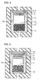
- One embodiment mode of the III-nitride single crystal growth method involving the present invention is characterized in being furnished with a step of , referring to Fig. 1 , placing source material 1 in a crucible 12, and a step of sublimating the source material 1 to grow an Al x Ga 1- x N (0 ⁇ x ⁇ 1, hereinafter) single crystal 4 in the crucible 12, and characterized in that the source material 1 is composed of Al y Ga 1- y N (0 ⁇ y ⁇ 1, hereinafter) source 2 and impurity element 3, and the impurity element is at least a single kind element selected from the group consisting of IVb elements and IIa elements.
- the Al y Ga 1- y N source 2 that is a direct source material for forming the Al x Ga 1- x N single crystal 4, together with at least a single kind of impurity element 3 selected from the group consisting of IVb elements and IIa elements, the rate at which the Al x Ga 1- x N single crystal 4 grows heightens, to grow bulk Al x Ga 1- x N single crystal 4 of low dislocation density and favorable crystallinity stably.
- Such an impurity element E is believed to react with Al to become Al p E q (g) (herein, p and q are positive numbers), and to act as material for transporting Al during growth of the Al x Ga 1- x N single crystal 4, heightening the crystal growth rate, as well as reducing dislocation densities to enhance crystallinity.
- the source material 1 includes the Al y Ga 1- y N source material 2 and at least a single kind of impurity element 3 selected from the group consisting of IVb elements and IIa elements, and the manner in which they are included in the source material is not limited. Therefore, the Al y Ga 1- y N source 2 collectively and the impurity element 3 collectively may be each arranged in the crucible 12, as illustrated in Fig. 1 . Also as illustrated in Fig.2 , the Al y Ga 1- y N source 2 and impurity element 3 may be arranged mixed together in the crucible 12. Furthermore, as illustrated in Fig.
- the Al y Ga 1- y N source material 2 may be arranged in the first source material compartment 12 p , and the impurity element 3 in the second source material compartment 12 q .
- the Al y Ga 1- y N source material 2 and impurity element 3 have is not particularly limited as long as the Al y Ga 1- y N source material 2 and impurity element 3 are in the form that enables controlling their relative proportions-that is, if in solid form, they may be block-like, granular, and powdery. It should be understood that in the situation in which the crucible 12, and the source material compartments 12 p , 12 q and crystal-growth compartment 12 r that will be explained hereinafter are formed of the impurity element 3, the concentration of the impurity element 3 cannot be controlled, which prevents above impurity element effect from being brought during Al x Ga 1- x N single crystal growth.
- the sublimation method utilized in this embodiment means the method in which, referring to Fig. 1 , the source material 1 including the Al y Ga 1- y N source 2 is sublimated, and then is solidified again to produce the Al x Ga 1- x N single crystal 4.
- a vertical high-frequency-heating sublimation furnace 10 as illustrated in Fig. 1 is employed, for example.
- the WC crucible 12 having a ventilation opening 12e is disposed in the center part of a reaction chamber 11 in the vertical sublimation furnace 10, with a heater 13 being provided around the crucible 12 so that ventilation from the inside of, to the outside of, the crucible 12 is secured.
- high-frequency heating coils 14 for heating the heater 13 are disposed centrally along the outer side of the reaction chamber 11. Additionally, an N 2 gas inlet 11 a for passing N 2 gas into the reaction chamber 11 outside of the crucible 12, an outlet 11 c , and radiation thermometers 15 for measuring the temperatures of the bottom and top sides of the crucible 12 are provided to the ends of the reaction chamber 11.
- the Al x Ga 1- x N single crystal 4 can be manufactured employing above vertical sublimation furnace 10.
- the source material 1 including the Al y Ga 1- y N source 2 and impurity element 3 are housed in the lower part of the crucible 12, and with the N 2 gas being continuously passed into the reaction chamber 11, the temperature in the crucible 12 is raised by heating the heater 13 employing the high-frequency heating coils 14, and the temperature of the part in the crucible 12 where the source material 1 is housed is kept higher than that of the rest in the crucible 12, to sublimate the Al x Ga 1- x N and impurity element in the source material 1, and then the Al x Ga 1- x N is solidified again in the upper part of the crucible 12 to grow the Al x Ga 1- x N single crystal 4.
- the Al x Ga 1- x N single crystal 4 As a result of, during the growth of the Al x Ga 1- x N single crystal 4, bringing the temperature of the part in the crucible 12 where the source material 1 is housed to a level of 1600°C to 2300°C, and making the temperature of the upper part in the crucible 12 (where the Al x Ga 1- x N single crystal 4 is grown) approximately 10°C to 200°C lower than that of the part in the crucible 12 where the source material 1 is housed, the Al x Ga 1- x N single crystal 4 of favorable crystallinity can be obtained. Moreover, passing N 2 gas into the reaction chamber 11 outside the crucible 12 continuously also during crystal growth reduces the mixing of the impurities into the Al x Ga 1- x N single crystal 4.
- impurity element is at least a single kind element selected from the group consisting of IVb elements and IIa elements.
- the IVb and IIa elements which are believed to act as materials for transporting Al, heightens Al x Ga 1- x N single crystal growth rate and enhances crystallinity.
- Group IVb elements mean elements categorized into Group IVb in periodic table of the elements, and C (carbon), Si (silicon), and Ge (germanium) fall into the Group IVb.
- Group IIa elements which are called also alkaline earth metal, mean elements categorized into Group IIa in periodic table of the elements, and Mg (magnesium) and Ca (calcium) fall into the Group IIa.
- a plurality of impurity elements selected from above IVb and IIa elements can be used at the same time. Selecting a plurality of elements (for example, Si and C) from IVb elements is less than optimal, however, because the selected plurality of elements (Si and C) react with each other to form a stable compound (SiC), and thus lose the effect of acting as materials for transporting Al, sometimes resulting in failure to offer advantages sufficient to heighten Al x Ga 1- x N single crystal growth and to enhance crystallinity.
- the impurity element is preferably any one of Ai, C, and Ge.
- any one specific element picked out from IVb elements-particularly, Si, C, or Ge among them- is preferable from the perspective of heightening Al x Ga 1- x N single crystal growth rate and of enhancing crystallinity.
- ratio n E / n A (simply, molar ratio n E / n A , hereinafter) of the number of moles n E of the atoms of the impurity element 3 to the number of moles n A of the Al atoms in the Al y Ga 1- y N source 2 is preferably between 0.01 and 0.5 inclusive, and more preferably, is between 0.05 and 0.5 inclusive.
- the impurity element has an attenuated effect of acting as material for transporting Al, and at a molar ratio n E / n A of more than 0.5, growth of the Al x Ga 1- x N single crystal 4 is blocked.
- ratio n E / n O (simply, molar ratio n E / n O , hereinafter) of the number of moles n E of the atoms of the impurity element 3 to the number of moles n O of the atoms of oxygen contained in the source material 1 is preferably between 2 and 1 ⁇ 10 4 inclusive.
- the molar ratio n E / n O is preferably between 3 and 1 ⁇ 10 4 inclusive, and more preferably, is between 10 and 1 ⁇ 10 4 inclusive.
- the number of moles of the atoms of oxygen contained in the source material 1 is calculated from the production of carbon monoxide generated by reacting the predetermined amount of the source material 1 with an excessive amount of carbon.
- the impurity element 3 can be used in form of various compounds, in addition to form of single elemental substance. Oxides are not preferable, however, because they block crystal growth-for example, they increases oxygen content in the whole source material 1, and makes the above action the present invention intends of the impurity element 3 less effective.
- the source material 1 in which the impurity element 3 is added to the Al y Ga 1- y N source 2 can be heat-treated prior to growth of the Al x Ga 1- x N single crystal 4.
- the source material 1 in which the impurity element 3 is added to the Al y Ga 1- y N source 2 can be heat-treated prior to growth of the Al x Ga 1- x N single crystal 4.
- ratio of the number of moles n E of the atoms of the impurity element 3 to the number of moles n A of the Al atoms in the Al y Ga 1- y N source 2 that is, molar ratio n E / n A
- oxygen mole content ⁇ MO in the source material 1 preferably fall within above ranges.
- the crucible 12 is not particularly limited, but from the perspective of stably growing the Al x Ga 1- x N single crystal 4, the crucible 12 is preferably formed from materials that do not react with the Al y Ga 1- y N source 2 or impurity element 3, or that suffer little degradation during growth of the Al x Ga 1- x N single crystal 4 without discharging the impurity element 3 into the atmosphere in which crystal is grown, and preferably, is formed particularly from metal carbide.
- the metal carbide for forming the crucible 12 include TiC, XrC, NbC, TaC, MoC, and WC.
- Embodiment Mode 1 Another embodiment mode of the III-nitride single crystal growth method involving the present invention is common to Embodiment Mode 1 in being provided with, referring to Figs. 1 and 2 , the step of arranging the source material 1 n the crucible 12 and the step of sublimating the source material 1 to grow the Al x Ga 1- x N single crystal 4 in the crucible 12, and in that the source material 1 includes the Al y Ga 1- y N source 2 and the impurity element 3, and the impurity 3 is at least one selected from the group consisting of IVb elements and IIa elements.
- Embodiment mode 1 in which the Al y Ga 1- y N source 2 collectively and the impurity element 3 collectively are each arranged in the crucible 12 differs in that, referring to Fig. 2 , the source material 1 in which the Al y a 1- y N source 2 and impurity element 3 are mixed together is arranged in crucible 12 in above step.
- the material source 1 arranged in the crucible 12 in this embodiment mode is a mixture of the Al y Ga 1- y N source 2 and impurity element 3, the distribution of the Al y Ga 1- y N gas source and impurity element gas within the crucible 12 after the sublimation of the source material 1 is more readily uniformed, and thus the Al x Ga 1- x N single crystal 4 is more stably grown.
- the impurity element is any one of Si, C and Ge
- molar ratio n E / n A is from 0.01 to 0.5 inclusive
- molar ratio n E / n O is from 3 to 1 ⁇ 10 4 inclusive
- the crucible 12 is composed of metal carbide.
- a further embodiment mode of the III-nitride single crystal growth method involving the present invention is common to Embodiment Mode 1, referring to Figs. 1 and 3 , in being provided with the step of arranging the source material 1 in the crucible 12 and the step of sublimating the source material 1 to grow the Al x Ga 1- x N single crystal 4 in the crucible 12, an in that the source material 1 includes the Al y Ga 1- y N source 2 and the impurity element 3, and the impurity 3 is at least one selected from the group consisting of IVb elements and IIa elements.
- Embodiment Mode 1 in which the Al y Ga 1- y N source 2 collectively and the impurity element 3 collectively are each arranged in the crucible 12, and from Embodiment Mode 2 in which the Al y Ga 1- y N source 2 and impurity element 3 are arranged mixed together in the crucible 12, however, this embodiment mode differs in that, referring to Fig.
- the first source material compartment 12 p , second source material compartment 12 q and crystal-growth compartment 12 r are provided in the crucible 12, with the ventilation openings 12 a , 12 b , and 12 c being provided between the first and the second source material compartments 12 p , 12 q , and between at least one of them and the crystal-growth compartment 12 r , and the Al y Ga 1- y N source 2 is arranged in the first source material compartment 12 p , with the impurity element 3 being arranged in the second source material compartment 12 q .
- the Al y Ga 1- y N source 2 and impurity element 3 are arranged respectively in the first and second source material compartments 12 p , 12 q where gases in the compartments can be exchanged via the ventilation opening 12a, the distribution of the Al y Ga 1- y N gas source and impurity element gas within the crucible 12 in which the source material 1 has sublimated can made more uniform without direct contact between the Al y Ga 1- y N source 2 and impurity element 3, enabling more stable growth of the Al x Ga 1- x N single crystal 4.
- FIG. 3 illustrates the example in which the ventilation openings 12 a , 12 b , and 12 c are provided respectively between the first and the second source material compartments 12 p , 12 q , between the first source material compartment 12 p and the crystal-growth compartment 12 r , and between the second source material compartment 12q and the crystal-growth compartment 12 r , but in this embodiment mode, as to ventilation openings 12b and 12 c , advantageously at least one of them may be provided.
- the impurity element is any one of Si, C and Ge
- molar ratio n E / n A is from 0.01 to 0.5 inclusive
- molar ratio n E / n O is from 2 to 1 ⁇ 10 4 inclusive
- the crucible 12 is formed from metal carbide.
- FIG. 1 Yet another embodiment mode of the III-nitride single crystal growth method involving the present invention is common to Embodiment Mode 1, referring to Figs. 1 and 4 , in being provided with the step of arranging the source material 1 in the crucible 12 and the step of sublimating the source material 1 to grow the Al x Ga 1- x N single crystal 4 in the crucible 12, and in that the source material 1 includes the Al y Ga 1- y N source 2 and impurity element 3, and the impurity 3 is at least one selected from the group consisting of IVb elements and IIa elements.
- Embodiment Modes 1 through 3 in which no undersubstrate is arranged in the crucible 12 and the Al x Ga 1- x N single crystal 4 is grown on the opposite end of the crucible 12 from the end where the source material 1 is arranged, however, this embodiment mode differs in that, referring to Fig. 4 , an undersubstrate 9 is also placed in the crucible 12 and the Al x Ga 1- x N single crystal 4 is grown on the undersubstrate 9.
- Fig. 4 an undersubstrate 9 is also placed in the crucible 12 and the Al x Ga 1- x N single crystal 4 is grown on the undersubstrate 9.
- the source material 1 in which the Al y Ga 1- y N source 2 and impurity element 3 has been mixed is arranged in the crucible 12 (the source material 1 is arranged in the same manner as in Embodiment ⁇ Mode 2), as to how to arrange the source material, the same manners as in Embodiment Mode 1 and 3 can be adopted.
- the undersubstrate 9 is not particularly limited as long as the Al x Ga 1- x N single crystal 4 can be grown on it, so it may be any of a native substrate same with, and a non-native substrate different from, Al x Ga 1- x N single crystal in chemical composition. From the perspective of improving crystallinity, a non-native substrate slightly differing from a native substrate or Al x Ga 1- x N single crystal in lattice constant is preferable. Furthermore, from the perspective of producing bulk Al x Ga 1- x N single crystal, the undersubstrate 9 is preferably a bulk substrate large in diameter. Form this perspective, SiC, Al 2 O 3 , GaN substrates are preferably utilized.
- an undersubstrate with a diameter of 2 inches or more enables growth of a bulk Al x Ga 1- x N single crystal having a diameter of 2 inches or more.
- wafers with a diameter of 1 inch, 2inches, 4 inches, and other predetermined sizes are generally manufactured. That is to say, although 1 inch is 2.54 cm in unit conversion, a diameter of 2 inches means one of the sizes representing a diameter of wafers such as substrates and crystals, so that diameter, which is not limited exactly to 5.08 cm, includes manufacturing errors.
- the impurity element is any one of Si, C and Ge
- molar ratio n E / n A is from 0.01 to 0.5 inclusive
- molar ratio n E / n O is from 3 to 1 ⁇ 10 4 inclusive
- the crucible 12 is formed from metal carbide.
- Still another embodiment mode of the III-nitride single crystal growth method involving the present invention is further furnished with a step of, referring to Figs. 1 , 5 , and 6 , sublimating Al t Ga 1- t N (0 ⁇ t ⁇ 1) source 7 to grow onto the Al x Ga 1- x N single crystal 4 grown by any of the growth methods in embodiment modes 1 through 4 a Al s Ga 1- s N (0 ⁇ S ⁇ 1) single crystal (5) with a lower concentration of the impurity element 3 compared with Al x Ga 1- x N single crystal 4.
- an Al x 2 Ga 1- x 2 N single crystal 5 having favorable crystallinity, low concentration of the contained impurity element 3, and high general versatility can be grown onto0 the Al x Ga 1- x N single crystal 4 of favorable crystallinity.
- the type and concentration of impurity element contained in the Al x Ga 1- x N single crystal 4 and Al s Ga 1- s N single crystal 5 can be measured by secondary ion mass spectroscopy (SIMS).
- the step of sublimating the Al t Ga 1- t N ((0 ⁇ t ⁇ 1) source 7 to grow onto the Al x Ga 1- x N single crystal 4 the Al s Ga 1- s N (0 ⁇ S ⁇ 1) single crystal 5 having a lower concentration of the contained impurity element 3 compared with the Al x Ga 1- x N single crystal 4 is not particularly limited, so the step can be performed with, referring to Figs. 5 and 6 , the Al t Ga 1- t N source 7, not above impurity element, being arranged as source material in the crucible 12.
- the Al t Ga 1- t N source 7 not above impurity element
- Al s Ga 1- s N single crystal is further grown onto the Al x Ga 1- x N single crystal 4 that has been grown onto the undersubstrate 9. Moreover, referring to Fig. 6 , the grown Al x Ga 1- x N single crystal 4 is processed into a substrate, and then the Al s Ga 1- s N single crystal 5 is further grown onto the this substrate.
- the chemical composition of the Al s Ga 1- s N single crystal is preferably close to, and more preferably, similar to, that of the Al x Ga 1- x N single crystal.
- the chemical composition of the Al t Ga 1- t N source 7 for producing the Al s Ga 1- s N single crystal 5 of the predetermined chemical composition is defined.
- AlN powder (the Al y Ga 1- y N source 2) and Si powder (the impurity element 3) were mixed so that molar ratio n E / n A of Si atoms (atoms of the impurity element 3) in the Si powder to Al atoms in the AlN powder (the Al y Ga 1- y N source 2) was made 0.05, and were arranged as the source material 1 in the bottom part of the WC crucible 12. Furthermore, a SiC substrate 2 inches (5.08 cm) in diameter was arranged as the undersubstrate 9 in the top part of the crucible 12.
- oxygen mole percent ⁇ MO in the AlN powder and Si powder was 0.1
- molar ratio n E / N O of Si atoms (atoms of the impurity element 3) of the Si powder to the atoms of oxygen contained in the AlN powder and Si powder (source material 1) was 20.
- WC material that is an undersubstrate protector 16 is closely attached to the back side of the SiC substrate (the undersubstrate 9).
- the temperature in the crucible 12 was raised employing the high-frequency coils 14. While the temperature in the crucible 12 was rising, with temperature in the part of the crucible 12 where the SiC substrate (the undersubstrate 9) was arranged being kept higher than that in the part of the crucible 12 where the source material 1 was arranged, the front side of the SiC substrate (the under substrate 9) was cleaned by means of etching, and at the same time the impurities discharged from the SiC substrate (the undersubstrate 9) and the inside of the crucible 12 were removed though the ventilation opening 12 e .
- the temperature in the part of the crucible 12 where the source material 1 was arranged was brought to 2100°C
- the temperature in the part of the crucible 12 where the SiC substrate (the undersubstrate 9) was arranged was brought to 2000°C, to sublimate AlN and C from the source material 1, and the AlN was solidified again on the SiC substrate (the undersubstrate 9 ) arranged in the top part of the crucible 12 to grow AlN single crystal (the Al x Ga 1- x N single crystal 4).
- the N 2 gas was passed into the reaction chamber outside the crucible 12 continuously also during AlN sigle crystal (the Al x Ga 1- x N single crystal 4) growth, and the amounts of N 2 gas introduction and emission is controlled so that the partial pressure of gas in the reaction chamber 11 outside the crucible 12 is brought to a level of 10 1.3 hPa to 1013 hPa.
- the crucible 12 was cooled to room temperature, and thus the AlN crystal was obtained.
- the obtained AlN single crystal (the Al x Ga 1- x N single crystal 4) was a large 2 inches (5.08 cm) in diameter ⁇ 4 mm in thickness with a uniform thickness, and its growth rate was 133 ⁇ m/hr.
- the full-width at half-maximum of X-ray diffraction peak on the AlN single crystal (0002) face is a small 70 arcsec, and crystallinity was preferable.
- the AlN single crystal dislocation density which was calculated by etch-pit density (EPD: the method of calculating as dislocation density the density of pits forming on front side as a result of etching), was a low 5.0 ⁇ 10 5 cm -2 . The results are set forth in Table 1.
- AlN single crystal (the Al x Ga 1- x N single crystal 4) was grown in the same manner as in Embodiment 1. Although the obtained AlN single crystal (the Al x Ga 1- x N single crystal 4) was 2 inches (5.08 cm) in diameter, its thickness is nonuniform-0.4 mm on average-and its growth rate was 13 ⁇ m/hr. In addition, the areas in which AlN single crystal has not grown was found on the SiC substrate (the undersubstrate 9).
- the source material 1 Apart from employing as the source material 1 the mixture in which the AlN powder (the Al y Ga 1- y N source 2) and Si powder (impurity element 3) were mixed so that molar ratio n E / n A of Si atoms in the Si powder to Al toms in the AlN powder was 0.01 (oxygen mole percent ⁇ MO in the source material 1 was 0.1 mol %, and molar ratio n E / n O of Si atoms in the Si powder to the atoms of oxygen contained in the source material 1 was 4), AlN single crystal (the Al x Ga 1- x N single crystal 4) was grown in the same manner as in Embodiment 1.
- the obtained AlN single crystal (the Al x Ga 1- x N single crystal 4) was a large 2 inches (5.08 cm) in diameter ⁇ 3 mm in thickness with a uniform thickness, and its growth rate was 100 ⁇ m/hr.
- the full-width at half-maximum of X-ray diffraction peak on the AlN single crystal (0002) face was a small 500 arcsec, and crystallinity was preferable.
- the AlN single crystal dislocation density was a low 6.0 ⁇ 10 5 cm -2 . The results are set forth in Table 1.
- the source material 1 Apart from employing as the source material 1 the mixture in which AlN powder (the Al y Ga 1- y N source 2) and Si powder (the impurity element 3) were mixed so that molar ratio n E / n A of Si atoms in the Si powder to Al toms in the AlN powder was 0.3 (oxygen mole percent ⁇ MO in the source material 1 was 0.1 mol %, and molar ratio n E / n O of Si atoms in the Si powder to the atoms of oxygen contained in the source material 1 was 60), AlN single crystal (the Al x Ga 1- x N single crystal 4) was grown in the same manner as in Embodiment 1.
- AlN powder the Al y Ga 1- y N source 2
- Si powder the impurity element 3
- the obtained AlN single crystal (the Al x Ga 1- x N single crystal 4) was a large 2 inches (5.08 cm) in diameter ⁇ 4.5 mm in thickness with a uniform thickness, and its growth rate was 150 ⁇ m/hr.
- the full-width at half-maximum of X-ray diffraction peak on the AlN single crystal (0002) face was a small 100 arcsec, and crystallinity was preferable.
- the AlN ingle crystal dislocation density was a low 7.0 ⁇ 10 5 cm -2 . The results are set forth in Table 1.
- the source material 1 Apart from employing as the source material 1 the mixture in which AlN powder (the Al y Ga 1- y N source 2) and Si powder (the impurity element 3) were mixed so that molar ratio n E / n A of Si atoms in the Si powder to Al toms in the AlN powder was 0.5 (oxygen mole percent ⁇ MO in the source material 1 was 0.1 mol %, and molar ratio n E / n O of Si atoms in the Si powder to the atoms of oxygen contained in the source material 1 was 200), AlN single crystal (the Al x Ga 1- x N single crystal 4) was grown in the same manner as in Embodiment 1.
- AlN powder the Al y Ga 1- y N source 2
- Si powder the impurity element 3
- the obtained AlN single crystal (the Al x Ga 1- x N single crystal 4) was a large 2 inches (5.08 cm) in diameter ⁇ 5 mm in thickness with a uniform thickness, and its growth rate was 166 ⁇ m/hr.
- the full-width at half-maximum of X-ray diffraction peak on the AlN single crystal (0002) face was a small 120 arcsec, and crystallinity was preferable.
- the AlN single crystal dislocation density was a low 8.0 ⁇ 10 5 cm -2 . The results are set forth in Table 1.
- the source material 1 Apart from employing as the source material 1 the mixture in which AlN powder (the Al y Ga 1- y N source 2) and C (carbon) powder (the impurity element 3) were mixed so that molar ratio n E / n A of C atoms in the C powder to Al toms in the AlN powder was 0.01 (oxygen mole percent ⁇ MO in the source material 1 was 0.1 mol %, and molar ratio n E / n O of C atoms in the C powder to atoms in the oxygen contained in the source material 1 was 4), AlN single crystal (the Al x Ga 1- x N single crystal 4) was grown in the same manner as in Embodiment 1.
- AlN powder the Al y Ga 1- y N source 2
- C (carbon) powder the impurity element 3
- the obtained AlN single crystal (the Al x Ga 1- x N single crystal 4) was a large 2 inches (5.08 cm) in diameter ⁇ 4.8 mm in thickness with a uniform thickness, and its growth rate was 150 ⁇ m/hr.
- the full-width at half-maximum of X-ray diffraction peak on the AlN single crystal (0002) face was a small 45 arcsec, and crystallinity was preferable.
- the AlN single crystal dislocation density was a low 9.0 ⁇ 10 4 cm -2 .
- Table 1 The results are set forth in Table 1.
- the source material 1 Apart from employing as the source material 1 the mixture in which AlN powder (the Al y Ga 1- y N source 2) and C (carbon) powder (the impurity element 3) were mixed so that molar ratio n E / n A of C atoms in the C powder to Al toms in the AlN powder was 0.05 (oxygen mole percent ⁇ MO in the source material 1 was 0.1 mol %, and the molar ratio n E / n O of C atoms in the C powder to atoms of the oxygen contained in the source material 1 was 20), AlN single crystal (the Al x Ga 1- x N single crystal 4) was grown in the same manner as in Embodiment 1.
- AlN powder the Al y Ga 1- y N source 2
- C (carbon) powder the impurity element 3
- the obtained AlN single crystal (the Al x Ga 1- x N single crystal 4) was a large 2 inches (5.08 cm) in diameter ⁇ 9 mm in thickness with a uniform thickness, and its growth rate was 300 ⁇ m/hr.
- the full-width at half-maximum of X-ray diffraction peak on the AlN single crystal (0002) face was a small 30 arcsec, and crystallinity was preferable.
- the AlN single crystal dislocation density was a low 5.0 ⁇ 10 4 cm -2 . The results are set forth in Table 1.
- the source material 1 Apart from employing as the source material 1 the mixture in which AlN powder (the Al y Ga 1- y N source 2) and C (carbon) powder (the impurity element 3) were mixed so that molar ratio n E / n A of C atoms in the C powder to Al toms in the AlN powder was 0.3 (oxygen mole percent ⁇ MO in the source material 1 was 0.1 mol %, and molar ratio n E / n O of C atoms in the C powder to atoms of the oxygen contained in the source material 1 was 60), AlN single crystal (the Al x Ga 1- x N single crystal 4) was grown in the same manner as in Embodiment 1.
- AlN powder the Al y Ga 1- y N source 2
- C (carbon) powder the impurity element 3
- the obtained AlN single crystal (the Al x Ga 1- x N single crystal 4) was a large 2 inches (5.08 cm) in diameter ⁇ 10.5 mm in thickness with a uniform thickness, and its growth rate was 350 ⁇ m/hr.
- the full-width at half-maximum of X-ray diffraction peak on the AlN single crystal (0002) face was a small 30 arcsec, and crystallinity was preferable.
- the AlN single crystal dislocation density was a low 6.0 ⁇ 10 4 cm -2 . The results are set forth in Table I.
- the source material 1 Apart from employing as the source material 1 the mixture in which AlN powder (the Al y Ga 1- y N source 2) and C (carbon) powder (the impurity element 3) were mixed so that the molar ratio n E / n A of C atoms in the C powder to Al toms in the AlN powder was 0.5 (oxygen mole percent ⁇ MO in the source material 1 was 0.1 mol %, and molar ratio n E / n O of C atoms in the C powder to atoms of the oxygen contained in the source material 1 was 200), AlN single crystal (the Al x Ga 1- x N single crystal 4) was grown in the same manner as in Embodiment 1.
- AlN powder the Al y Ga 1- y N source 2
- C (carbon) powder the impurity element 3
- the obtained AlN single crystal (the Al x Ga 1- x N single crystal 4) was a large inches (5.08 cm) in diameter ⁇ 12 mm in thickness with a uniform thickness, and its growth rate was 400 ⁇ m/hr.
- the full-width at half-maximum of X-ray diffraction peak on the AlN single crystal (0002) face was a small 45 arcsec, and crystallinity was preferable.
- the AlN single crystal dislocation density was a low 1.0 ⁇ 10 5 cm -2 .
- Table I The results are set forth in Table I.
- the source material 1 Apart from employing as the source material 1 the mixture in which AlN powder (the Al y Ga 1- y N source 2) and Ge powder (the impurity element 3) were mixed so that molar ratio n E / n A of Ge atoms in the Ge powder to Al toms in the AlN powder was 0.05 (oxygen mole percent ⁇ MO in the source material 1 was 0.1 mol %, and molar ratio n E / n O of Ge atoms in the Ge powder to atoms of the oxygen contained in the source material 1 was 20), AlN single crystal (the Al x Ga 1- x N single crystal 4) was grown in the same manner as in Embodiment 1.
- AlN powder the Al y Ga 1- y N source 2
- Ge powder the impurity element 3
- the obtained AlN single crystal (the Al x Ga 1- x N single crystal 4) was a large 2 inches (5.08 cm) in diameter ⁇ 6 mm in thickness with a uniform thickness, and its growth rate was 200 ⁇ m/hr.
- the full-width at half-maximum of X-ray diffraction peak on the AlN single crystal (0002) face was a small 50 arcsec, and crystallinity was preferable.
- the AlN single crystal dislocation density was a low 8.0 ⁇ 10 4 cm -2 .
- Table II The results are set forth in Table II.
- the source material 1 Apart from employing as the source material 1 the mixture in which AlN powder (the Al y Ga 1- y N source 2) and Ca powder (the impurity element 3) were mixed so that molar ratio n E / n A of Ca atoms in the Ca powder to Al toms in the AlN powder was 0.05 (oxygen mole percent ⁇ MO in the source material 1 was 0.1 mol %, and molar ratio n E / n O of Ca atoms in the Ca powder to atoms of the oxygen contained in the source material 1 was 20), AlN single crystal (the Al x Ga 1- x N single crystal 4) was grown in the same manner as in Embodiment 1.
- AlN powder the Al y Ga 1- y N source 2
- Ca powder the impurity element 3
- the obtained AlN single crystal (the Al x Ga 1- x N single crystal 4) was a large 2 inches (5.08 cm) in diameter ⁇ 3 mm in thickness with a uniform thickness, and its growth rate was 100 ⁇ m/hr.
- the full-width at half-maximum of X-ray diffraction peak on the AlN single crystal (0002) face was a small 120 arcsec, and crystallinity was preferable.
- the AlN single crystal dislocation density was a low 6.0 ⁇ 10 6 cm -2 .
- Table II The results are set forth in Table II.
- the source material 1 Apart from employing as the source material 1 the mixture in which AlN powder (the Al y Ga 1- y N source 2) and Mg powder (the impurity element 3) were mixed so that molar ratio n E / n A of Mg atoms in the Mg powder to Al toms in the AlN powder was 0.05 (oxygen mole percent ⁇ MO in the source material 1 was 0.1 mol %, and molar ratio n E / n O of Mg atoms in the Mg powder to atoms of the oxygen contained in the source material 1 was 20), AlN single crystal (the Al x Ga 1- x N single crystal 4) was grown in the same manner as in Embodiment 1.
- AlN powder the Al y Ga 1- y N source 2
- Mg powder the impurity element 3
- the obtained AlN single crystal (the Al x Ga 1- x N single crystal 4) was a large 2 inches (5.08 cm) in diameter ⁇ 2 mm in thickness with a uniform thickness, and its growth rate was 67 ⁇ m/hr.
- the full-width at half-maximum of X-ray diffraction peak on the AlN single crystal (0002) face was a small 150 arcsec, and crystallinity was preferable.
- the AlN single crystal dislocation density was a low 7.0 ⁇ 10 5 cm -2 .
- Table II The results are set forth in Table II.
- the source material 1 Apart from employing as the source material 1 the mixture in which AlN powder (the Al y Ga 1- y N source 2) and Si and Ca powders (impurity element 3) were mixed as the source material 1 so that molar ratio n E / n A of Si atoms in the Si powder to, and that of Ca atoms in the Ca powder to, Al atoms in the AlN powder were respectively 0.025 and 0.025 (oxygen mole percent ⁇ MO in the source material 1 was 0.1m mol %, and molar ratio n E / n O of Si atoms of the Si powder to, and that of Ca atoms of the Ca powder to, atoms of the oxygen contained in the source material 1 were respectively 10 and 10), AlN single crystal (the Al x Ga 1- x N single crystal 4) was grown in the same manner as in Embodiment 1.
- AlN powder the Al y Ga 1- y N source 2
- Si and Ca powders impurity element 3
- the obtained AlN single crystal (the Al x Ga 1- x N single crystal 4) was a large 2 inches (5.08 cm) in diameter ⁇ 4.5 mm in thickness with a uniform thickness, and its growth rate was 150 ⁇ m/hr.
- the full-width at half-maximum of X-ray diffraction peak on the AlN single crystal (0002) face was a small 70 arcsec, and crystallinity was preferable.
- the AlN single crystal dislocation density was a low 5.0 ⁇ 10 5 cm -2 . The results are set forth in Table II.
- the source material 1 Apart from employing as the source material 1 the mixture in which AlN powder (the Al y Ga 1- y N source 2) and C and Ca powders (impurity element 3) were mixed so that molar ratio n E / n A of C atoms in the C powder to, and that of Ca atoms in the Ca powder to, Al atoms in the AlN powder was respectively 0.025 and 0.025 (oxygen mole percent ⁇ MO in the source material 1 was 0.1 mol %, and molar ratio n E / n O of C atoms in the C powder to, and that of Ca atoms in the Ca powder to, atoms of the oxygen contained in the source material 1 was respectively 10 and 10), AlN single crystal (the Al x Ga 1- x N single crystal 4) was grown in the same manner as in Embodiment 1.
- AlN powder the Al y Ga 1- y N source 2
- C and Ca powders impurity element 3
- the obtained AlN single crystal (the Al x Ga 1- x N single crystal 4) was a large 2 inches (5.08 cm) in diameter ⁇ 6 mm in thickness with a uniform thickness of 6 mm, and its growth rate was 200 ⁇ m/hr.
- the full-width at half-maximum of X-ray diffraction peak on the AlN single crystal (0002) face was a small 45 arcsec, and crystallinity was preferable.
- the AlN single crystal dislocation density was s low 8.0 ⁇ 10 4 cm -2 . The results are set forth in Table II.
- the source material 1 Apart from employing as the source material 1 the mixture in which Al 0.65 Ga 0.35 N powder (the Al y Ga 1- y N source 2) and C powder were mixed so that molar ratio n E / n A of C atoms in the C powder to Al atoms in the AlN powder was 0.05 (oxygen mole percent ⁇ MO in the source material 1 was 0.1 mol %, and molar ratio n E / n O of C atoms in the C powder to atoms of oxygen contained in the source material 1 was 20), AlN single crystal (the Al x Ga 1- x N single crystal 4) was grown in the same manner as in Embodiment 1.
- the chemical composition of the obtained single crystal measured Al 0.8 Ga 0.2 N by x-ray photoelectron Spectroscopy. That is to say, the obtained Al x Ga 1- x N single crystal 4 included Al atoms at a greater ratio compared with that of the Al y Ga 1- y N source 2. The possible reason is that C atoms promoted the transportation of Al.
- the obtained Al 0.8 Ga 0.2 N single crystal (the Al x Ga 1- x N single crystal 4) was a large 2 inches (5.08 cm) in diameter ⁇ 8 mm in thickness with a uniform thickness, and its growth rate was 266 ⁇ m/hr.
- the full-width at half-maximum of X-ray diffraction peak on the AlN single crystal (0002) face was a small 50 arcsec, and crystallinity was preferable. Furthermore, the Al 0.8 Ga 0.2 N single crystal dislocation density was a low 1.0 ⁇ 10 5 cm -2 .
- Table II The results are set forth in Table II.
- n E / n A of the impurity element atoms to Al atoms in the Al y Ga 1- y N source included in the source material to be sublimated 0.01 to 0.5 inclusive
- molar ratio n E / n O of the impurity element atoms to the atoms oxygen contained in the source material to be sublimated 1 ⁇ 10 4 or less, kept crystal growth rate high, and enabled obtaining lower-dislocation-density Al x Ga 1- x N single crystal of favorable crystallinity.
- an AlN single crystal (the Al x Ga 1- x N single crystal 4) 2inches (5.08 cm) in diameter ⁇ 4.8 mm in thickness was grown.
- this AlN single crystal (the Al x Ga 1- x N single crystal 4)
- its dislocation density was a low 9.0 ⁇ 10 4 cm -2
- carbon atom concentration was approximately 1 ⁇ 10 18 cm -3
- oxygen atom concentration was 1 ⁇ 10 17 cm -3 or less.
- AlN powder was sublimated to grow another AlN single crystal (the Al s Ga 1- s N single crystal 5) onto the AlN single crystal (the Al x Ga 1- x N single crystal 4).
- Embodiment 5 Apart from making the temperature in the part of the crucible 12 where Al t Ga 1- t N source 7 was arranged 2200°C, and from making the temperature in the part end of the crucible 12 where the Al x Ga 1- x N single crystal 4 was grown 2050°C, crystal growth conditions was established as in Embodiment 5.
- the obtained AlN single crystal (the Al s Ga 1- s N single crystal 5), which was a large 2 inches (5.08 cm) in diameter ⁇ 1 mm in thickness with a uniform thickness.
- the AlN single crystal (the Al s Ga 1- s N single crystal 5) dislocation density was a low 2.0 ⁇ 10 5 cm -2 , and as to impurity concentration measured by SIMS, both carbon atom and oxygen atom concentrations were an extremely low 1 ⁇ 10 17 cm -3 .
Landscapes
- Chemical & Material Sciences (AREA)
- Engineering & Computer Science (AREA)
- Crystallography & Structural Chemistry (AREA)
- Materials Engineering (AREA)
- Metallurgy (AREA)
- Organic Chemistry (AREA)
- Inorganic Chemistry (AREA)
- Crystals, And After-Treatments Of Crystals (AREA)
Abstract
Description
- The present invention relates to methods of growing Group III nitride single crystals utilized in substrates for light-emitting diodes, electronic devices, semiconductor sensors, and other semiconductor devices. In particular the invention relates to a method of growing low-dislocation-density III-nitride single crystals of favorable crystallinity.
- III-nitride crystals such as Al x Ga1-x N (0 < x ≤ 1, likewise hereinafter) single crystals are extraordinarily useful as materials for building semiconductor devices such as light-emitting diodes, electronic devices, and semiconductor sensors.
- Examples that have been proposed of how to manufacture such III-nitride single crystals include vapor-phase techniques, particularly among which sublimation has been singled out from the perspective of obtaining crystals of satisfactory crystallinity with a narrow full-width at half-maximum for the X-ray diffraction peak. (Cf., for example, the specifications for
U.S. Pat. No. 5,858,086 (Patent Document 1),U.S. Pat. No. 6,296,956 (Patent Document 2), andU.S. Pat. No. 6,001,748 (Patent Document 3).) - However, with attempts to manufacture by sublimation a bulk III-nitride single crystal-for example (repeated similarly hereinafter), 2 inches (approximately 5.08 cm) in diameter × 2 mm or more in thickness-leading, due principally to the fact that no high-quality crystals ideal for undersubstrates exist, to problems of crystal growth being nonuniform and of increased dislocation density, crystallinity degradation, and incidents of polycrystalization, methods of stably growing Al x Ga1-x N single crystal of practicable size, and of low dislocation density and favorable crystallinity have yet to be proposed.
Patent Document 1:U.S. Pat. No. 5,858,086 specification
Patent Document 2:U.S. Pat. No. 6,296,956 specification
Patent Document 3:U.S. Pat. No. 6, 001, 748 specification - An object of the present invention is to make available a method of stably growing bulk III-nitride single crystal of low dislocation density and favorable crystallinity.
- The present invention is a III-nitride single-crystal growth method furnished with a step of placing source material in a crucible, and a step of sublimating the source material to grow an Al x Ga1-x N (0 < x ≤ 1) single crystal in the crucible, wherein the source material includes an Al y Ga1- yN (0 < y < 1) source and an impurity element, which is at least one selected from the group consisting of Group IVb elements and Group IIa elements.
- In a III-nitride single-crystal growth method involving the present invention, a first source material compartment, a second source material compartment, and a crystal-growth compartment are provided in the crucible, with openings for ventilation being provided between the first and the second source material compartments and between at least one of them and the crystal-growth compartment, and the Al y Ga1-y N source material can be arranged in the first source material compartment, and the impurity element in the second source material compartment.
- Furthermore, in a III-nitride single crystal growth method involving the present invention, the source material may be a mixture of the Al y Ga1-y N source and the impurity element. Moreover, as the impurity element, any one of Si, C, and Ge can be utilized. Additionally, in the source material, a ratio nE /nA of the number of moles nE of the impurity element atoms to the number of moles nA of the Al atoms in the Al y Ga1-y N source can be made 0.01 to 0.5 inclusive. Meanwhile, a ratio nE /no of the number of moles nE of the impurity element atoms to the number of moles no of atoms of the oxygen contained in the source material can be made 2 to 1 × 10⁴ inclusive. In addition, the crucible can be formed from metal carbide. Furthermore, an undersubstrate can be arranged in the crucible to grow Al x Ga1-x N single crystal on the undersubstrate. The Al x Ga1-x N single crystal diameter can be brought to a span of more than 2 inches. The III-nitride single crystal growth method can be further furnished with a step of sublimating an Al t Ga1-t N (0 < t ≤ 1) source to grow onto the Al x Ga1-x N single crystal monocrystalline Al s Ga1-s N (0 < S ≤ 1) with a lower impurity-element concentration by comparison to that of the Al x Ga1-x N single crystal.
- The present invention affords a method of stably growing bulk III-nitride single crystals of low dislocation density and of favorable crystallinity.
-
-
Fig. 1 is a cross-sectional schematic diagram for illustrating one mode of embodying a III-nitride single-crystal growth method involving the present invention. -
Fig. 2 is a cross-sectional schematic diagram for illustrating key features of a different mode of embodying a III-nitride single-crystal growth method involving the present invention. -
Fig. 3 is a cross-sectional schematic diagram for illustrating key features of a still different mode of embodying a III-nitride single-crystal growth method involving the present invention. -
Fig. 4 is a cross-sectional schematic diagram for illustrating key features of yet a different mode of embodying a III-nitride single-crystal growth method involving the present invention. -
Fig. 5 is a cross-sectional schematic diagram for illustrating key features of another different mode of embodying a III-nitride single-crystal growth method involving the present invention. -
Fig. 6 is a cross-sectional schematic diagram for illustrating key features of a further different embodiment mode of the III-nitride single crystal growth method involving the present invention. - 1: source material; 2: Al y Ga1-y N source; 3: impurity element; 4: Al x Ga1-x N single crystal; 5: Al s Ga1-s N single crystal; 7: Al t Ga1-t N source; 9: undersubstrate; 10: sublimation furnace; 11: reaction chamber; 11a: N2 gas inlet; 11b: N2 gas outlet; 12: crucible; 12a, 12b, 12c, and 12e: ventilation openings; 12p: first source material compartment; 12q: second source material compartment; 12r: crystal-growth compartment; 13: heater; 14: high-frequency heating coils; 15: radiation thermometers; 16: undersubstrate protector.
- One embodiment mode of the III-nitride single crystal growth method involving the present invention is characterized in being furnished with a step of , referring to
Fig. 1 , placingsource material 1 in acrucible 12, and a step of sublimating thesource material 1 to grow an Al x Ga1-x N (0 < x ≤ 1, hereinafter)single crystal 4 in thecrucible 12, and characterized in that thesource material 1 is composed of Al y Ga1-y N (0 < y ≤ 1, hereinafter) source 2 andimpurity element 3, and the impurity element is at least a single kind element selected from the group consisting of IVb elements and IIa elements. - By including, for the
sublimation source material 1, the Al y Ga1-y N source 2 that is a direct source material for forming the Al x Ga1-x Nsingle crystal 4, together with at least a single kind ofimpurity element 3 selected from the group consisting of IVb elements and IIa elements, the rate at which the Al x Ga1-x Nsingle crystal 4 grows heightens, to grow bulk Al x Ga1-x Nsingle crystal 4 of low dislocation density and favorable crystallinity stably. Such an impurity element E is believed to react with Al to become Al p E q (g) (herein, p and q are positive numbers), and to act as material for transporting Al during growth of the Al x Ga1-x Nsingle crystal 4, heightening the crystal growth rate, as well as reducing dislocation densities to enhance crystallinity. - Herein, it is sufficient that the
source material 1 includes the Al y Ga1-y N source material 2 and at least a single kind ofimpurity element 3 selected from the group consisting of IVb elements and IIa elements, and the manner in which they are included in the source material is not limited. Therefore, the Al y Ga1-y N source 2 collectively and theimpurity element 3 collectively may be each arranged in thecrucible 12, as illustrated inFig. 1 . Also as illustrated inFig.2 , the Al y Ga1-y N source 2 andimpurity element 3 may be arranged mixed together in thecrucible 12. Furthermore, as illustrated inFig. 3 , with a first and a secondsource material compartments ventilation opening 12a being provided in thecrucible 12, the Al y Ga1-y N source material 2 may be arranged in the firstsource material compartment 12p, and theimpurity element 3 in the secondsource material compartment 12q. - Moreover, what form the Al y Ga1-y N source material 2 and
impurity element 3 have is not particularly limited as long as the Al y Ga1-y N source material 2 andimpurity element 3 are in the form that enables controlling their relative proportions-that is, if in solid form, they may be block-like, granular, and powdery. It should be understood that in the situation in which thecrucible 12, and thesource material compartments growth compartment 12r that will be explained hereinafter are formed of theimpurity element 3, the concentration of theimpurity element 3 cannot be controlled, which prevents above impurity element effect from being brought during Al x Ga1-x N single crystal growth. Additionally, the chemical composition of the Al y Ga1-y N source material 2 and that of the Al x Ga1-x Nsingle crystal 4 produced from it coincides with each other when x = y = 1, but generally differ from each other except when x = y = 1 in accordance with the conditions on which the Al y Ga1-y N source is sublimated, and with the conditions on which the Al x Ga1-x Nsingle crystal 4 is grown. Once the sublimation conditions on the Al y Ga1-y N source and the growth conditions on the Al x Ga1-x Nsingle crystal 4 are defined, what chemical composition of the Al y Ga1-y N source material 2 is required to produce the Al x Ga1-x N single crystal having the given chemical composition is determined. - Herein, the sublimation method utilized in this embodiment means the method in which, referring to
Fig. 1 , thesource material 1 including the Al y Ga1-y N source 2 is sublimated, and then is solidified again to produce the Al x Ga1-x Nsingle crystal 4. During sublimation crystal growth, a vertical high-frequency-heating sublimation furnace 10 as illustrated inFig. 1 is employed, for example. TheWC crucible 12 having aventilation opening 12e is disposed in the center part of areaction chamber 11 in thevertical sublimation furnace 10, with aheater 13 being provided around thecrucible 12 so that ventilation from the inside of, to the outside of, thecrucible 12 is secured. Furthermore, high-frequency heating coils 14 for heating theheater 13 are disposed centrally along the outer side of thereaction chamber 11. Additionally, an N2 gas inlet 11a for passing N2 gas into thereaction chamber 11 outside of thecrucible 12, anoutlet 11c, andradiation thermometers 15 for measuring the temperatures of the bottom and top sides of thecrucible 12 are provided to the ends of thereaction chamber 11. - Referring to
Fig. 1 , in the following manner, the Al x Ga1-x Nsingle crystal 4 can be manufactured employing abovevertical sublimation furnace 10. Thesource material 1 including the Al y Ga1-y N source 2 andimpurity element 3 are housed in the lower part of thecrucible 12, and with the N2 gas being continuously passed into thereaction chamber 11, the temperature in thecrucible 12 is raised by heating theheater 13 employing the high-frequency heating coils 14, and the temperature of the part in thecrucible 12 where thesource material 1 is housed is kept higher than that of the rest in thecrucible 12, to sublimate the Al x Ga1-x N and impurity element in thesource material 1, and then the Al x Ga1-x N is solidified again in the upper part of thecrucible 12 to grow the Al x Ga1-x Nsingle crystal 4. - Herein, as a result of, during the growth of the Al x Ga1-x N
single crystal 4, bringing the temperature of the part in thecrucible 12 where thesource material 1 is housed to a level of 1600°C to 2300°C, and making the temperature of the upper part in the crucible 12 (where the Al x Ga1-x Nsingle crystal 4 is grown) approximately 10°C to 200°C lower than that of the part in thecrucible 12 where thesource material 1 is housed, the Al x Ga1-x Nsingle crystal 4 of favorable crystallinity can be obtained. Moreover, passing N2 gas into thereaction chamber 11 outside thecrucible 12 continuously also during crystal growth reduces the mixing of the impurities into the Al x Ga1-x Nsingle crystal 4. - In addition, during temperature rising in the
crucible 12, making the temperature of the part in thecrucible 12 except where the source material is housed higher than that of the part in thecrucible 12 where thesource material 1 is housed removes impurities via theventilation opening 12e from thecrucible 12, making it possible to further reduce the mixing of the impurities into the Al x Ga1-x Nsingle crystal 4. - In this embodiment mode, impurity element is at least a single kind element selected from the group consisting of IVb elements and IIa elements. The IVb and IIa elements, which are believed to act as materials for transporting Al, heightens Al x Ga1-x N single crystal growth rate and enhances crystallinity. Herein, Group IVb elements mean elements categorized into Group IVb in periodic table of the elements, and C (carbon), Si (silicon), and Ge (germanium) fall into the Group IVb. On the other hand, Group IIa elements, which are called also alkaline earth metal, mean elements categorized into Group IIa in periodic table of the elements, and Mg (magnesium) and Ca (calcium) fall into the Group IIa. A plurality of impurity elements selected from above IVb and IIa elements can be used at the same time. Selecting a plurality of elements (for example, Si and C) from IVb elements is less than optimal, however, because the selected plurality of elements (Si and C) react with each other to form a stable compound (SiC), and thus lose the effect of acting as materials for transporting Al, sometimes resulting in failure to offer advantages sufficient to heighten Al x Ga1-x N single crystal growth and to enhance crystallinity.
- Herein, the impurity element is preferably any one of Ai, C, and Ge. As to the above impurity element, any one specific element picked out from IVb elements-particularly, Si, C, or Ge among them-is preferable from the perspective of heightening Al x Ga1-x N single crystal growth rate and of enhancing crystallinity.
- In
source material 1 of this embodiment, ratio nE /nA (simply, molar ratio nE /nA , hereinafter) of the number of moles nE of the atoms of theimpurity element 3 to the number of moles nA of the Al atoms in the Al y Ga1-y N source 2 is preferably between 0.01 and 0.5 inclusive, and more preferably, is between 0.05 and 0.5 inclusive. At a molar ratio nE /nA of less than 0.01, the impurity element has an attenuated effect of acting as material for transporting Al, and at a molar ratio nE /nA of more than 0.5, growth of the Al x Ga1-x Nsingle crystal 4 is blocked. - Furthermore, ratio nE /nO (simply, molar ratio nE /nO , hereinafter) of the number of moles nE of the atoms of the
impurity element 3 to the number of moles nO of the atoms of oxygen contained in thesource material 1 is preferably between 2 and 1 × 10⁴ inclusive. Because a molar ratio nE /nO of less than 2 causes the relative number of moles of the atoms of theimpurity elements 3 to be small, making theimpurity element 3 as material for transporting Al less effective, and a molar ratio nE /nO of more than 1 × 10⁴ makes the relative number of moles of the atoms of theimpurity element 3 too much great, both molar ratio ranges blocks the growth of the Al x Ga1-x N single crystal. Form this perspective, the molar ratio nE /nO is preferably between 3 and 1 × 10⁴ inclusive, and more preferably, is between 10 and 1 × 10⁴ inclusive. Herein, the number of moles of the atoms of oxygen contained in thesource material 1 is calculated from the production of carbon monoxide generated by reacting the predetermined amount of thesource material 1 with an excessive amount of carbon. - Furthermore, the atoms of oxygen contained in the
source material 1 sometimes reduce above effect, of the action of theimpurity element 3, that the present invention intends, as well as directly block the growth of the Al x Ga1-x Nsingle crystal 4. For this reason, oxygen mole content α MO , in thesource material 1, defined by α MO = 100 × nO /nM employing the number of moles nM of the Al y Ga1-y N source 2 included in thesource material 1 and the number of moles nO of the atoms of oxygen contained in thesource material 1 is preferably 1 mole % or less, and more preferably, 0.1 mole % or less. - In this embodiment mode, in both particular situations in which the number of moles nE of atoms of the
impurity element 3 with respect to the number of moles nA of Al the atoms in the Al y Ga1-y N source 2 is particularly small (for example, a molar ratio nE /nA is less than 0.01 ), and in which the number of moles nE of atoms of theimpurity element 3 with respect to the number of moles nO of the atoms of oxygen contained in the Al y Ga1-y N source 2 is small (for example, a molar ratio nE /nO is less than3), stable crystal growth is prevented to cause lower crystal growth rate, resulting in crystallinity degradation. - Herein, the
impurity element 3 can be used in form of various compounds, in addition to form of single elemental substance. Oxides are not preferable, however, because they block crystal growth-for example, they increases oxygen content in thewhole source material 1, and makes the above action the present invention intends of theimpurity element 3 less effective. - Additionally, in this embodiment mode, the
source material 1 in which theimpurity element 3 is added to the Al y Ga1-y N source 2 can be heat-treated prior to growth of the Al x Ga1-x Nsingle crystal 4. Form the perspective of reducing any one specific element picked out from IVb element, and impurity element, excluding theimpurity element 3, selected from the group consisting of IIa elements, and of activating theimpurity element 3 in thesource material 1 and improving dispersibility, heat-treating thesource material 1 prior to the crystal growth is preferable. In the implementation of the heat-treatment of thesource material 1 prior to the crystal growth, in thesource material 1 that has undergone heat-treatment prior to crystal growth, ratio of the number of moles nE of the atoms of theimpurity element 3 to the number of moles nA of the Al atoms in the Al y Ga1-y N source 2 (that is, molar ratio nE /nA ), oxygen mole content α MO in thesource material 1, and ratio of the number of moles nE of the atoms of theimpurity element 3 to the number of moles nO of the atoms of oxygen contained in the source material 1 (that is, molar ratio nE /nO ) preferably fall within above ranges. - Moreover, in this embodiment mode, the
crucible 12 is not particularly limited, but from the perspective of stably growing the Al x Ga1-x Nsingle crystal 4, thecrucible 12 is preferably formed from materials that do not react with the AlyGa1-y N source 2 orimpurity element 3, or that suffer little degradation during growth of the Al x Ga1-x Nsingle crystal 4 without discharging theimpurity element 3 into the atmosphere in which crystal is grown, and preferably, is formed particularly from metal carbide. Preferable examples of the metal carbide for forming thecrucible 12 include TiC, XrC, NbC, TaC, MoC, and WC. In case that principally because theimpurity element 3 is discharged into the atmosphere in which crystal is grown, it is unintentionally provided to growing crystal, there is a possibility that content of theimpurity element 3 in the atmosphere varies during crystal growth (for example, the content gradually overages), and thus crystal growth is blocked. - Another embodiment mode of the III-nitride single crystal growth method involving the present invention is common to
Embodiment Mode 1 in being provided with, referring toFigs. 1 and2 , the step of arranging the source material 1 n thecrucible 12 and the step of sublimating thesource material 1 to grow the Al x Ga1-x Nsingle crystal 4 in thecrucible 12, and in that thesource material 1 includes the Al y Ga1-y N source 2 and theimpurity element 3, and theimpurity 3 is at least one selected from the group consisting of IVb elements and IIa elements. - From
Embodiment mode 1 in which the Al y Ga1-y N source 2 collectively and theimpurity element 3 collectively are each arranged in thecrucible 12, however, this embodiment mode differs in that, referring toFig. 2 , thesource material 1 in which the Al y a1-y N source 2 andimpurity element 3 are mixed together is arranged incrucible 12 in above step. - Because the
material source 1 arranged in thecrucible 12 in this embodiment mode is a mixture of the Al y Ga1-y N source 2 andimpurity element 3, the distribution of the Al y Ga1-y N gas source and impurity element gas within thecrucible 12 after the sublimation of thesource material 1 is more readily uniformed, and thus the Al x Ga1-x Nsingle crystal 4 is more stably grown. - Herein, preferably also in this embodiment mode, as in
Embodiment Mode 1, the impurity element is any one of Si, C and Ge, molar ratio nE /nA is from 0.01 to 0.5 inclusive, molar ratio nE /nO is from 3 to 1 × 10⁴ inclusive, and thecrucible 12 is composed of metal carbide. - A further embodiment mode of the III-nitride single crystal growth method involving the present invention is common to
Embodiment Mode 1, referring toFigs. 1 and3 , in being provided with the step of arranging thesource material 1 in thecrucible 12 and the step of sublimating thesource material 1 to grow the Al x Ga1-x Nsingle crystal 4 in thecrucible 12, an in that thesource material 1 includes the Al y Ga1-y N source 2 and theimpurity element 3, and theimpurity 3 is at least one selected from the group consisting of IVb elements and IIa elements. - From
Embodiment Mode 1 in which the Al y Ga1-y N source 2 collectively and theimpurity element 3 collectively are each arranged in thecrucible 12, and from Embodiment Mode 2 in which the Al y Ga1-y N source 2 andimpurity element 3 are arranged mixed together in thecrucible 12, however, this embodiment mode differs in that, referring toFig. 3 , the firstsource material compartment 12p, secondsource material compartment 12q and crystal-growth compartment 12r are provided in thecrucible 12, with theventilation openings source material compartments growth compartment 12r, and the Al y Ga1-y N source 2 is arranged in the firstsource material compartment 12p, with theimpurity element 3 being arranged in the secondsource material compartment 12q. - Because in this embodiment mode, the Al y Ga1-y N source 2 and
impurity element 3 are arranged respectively in the first and secondsource material compartments ventilation opening 12a, the distribution of the Al y Ga1-y N gas source and impurity element gas within thecrucible 12 in which thesource material 1 has sublimated can made more uniform without direct contact between the Al y Ga1-y N source 2 andimpurity element 3, enabling more stable growth of the Al x Ga1-x Nsingle crystal 4. - Herein,
Fig. 3 illustrates the example in which theventilation openings source material compartments source material compartment 12p and the crystal-growth compartment 12r, and between the secondsource material compartment 12q and the crystal-growth compartment 12r, but in this embodiment mode, as toventilation openings - In addition, preferably also in this embodiment mode, as in
Embodiment Modes 1 and 2, the impurity element is any one of Si, C and Ge, molar ratio nE /nA is from 0.01 to 0.5 inclusive, molar ratio nE /nO is from 2 to 1 × 10⁴ inclusive, and thecrucible 12 is formed from metal carbide. - Yet another embodiment mode of the III-nitride single crystal growth method involving the present invention is common to
Embodiment Mode 1, referring toFigs. 1 and4 , in being provided with the step of arranging thesource material 1 in thecrucible 12 and the step of sublimating thesource material 1 to grow the Al x Ga1-x Nsingle crystal 4 in thecrucible 12, and in that thesource material 1 includes the Al y Ga1-y N source 2 andimpurity element 3, and theimpurity 3 is at least one selected from the group consisting of IVb elements and IIa elements. - From
Embodiment Modes 1 through 3 in which no undersubstrate is arranged in thecrucible 12 and the Al x Ga1-x Nsingle crystal 4 is grown on the opposite end of thecrucible 12 from the end where thesource material 1 is arranged, however, this embodiment mode differs in that, referring toFig. 4 , anundersubstrate 9 is also placed in thecrucible 12 and the Al x Ga1-x Nsingle crystal 4 is grown on theundersubstrate 9. Herein, althoughFig. 4 shows that thesource material 1 in which the Al y Ga1-y N source 2 andimpurity element 3 has been mixed is arranged in the crucible 12 (thesource material 1 is arranged in the same manner as in Embodiment\ Mode 2), as to how to arrange the source material, the same manners as inEmbodiment Mode - In this embodiment mode, growing the Al x Ga1-x N
single crystal 4 onto theundersubstrate 9 enables more stable growth of the Al x Ga1-x Nsingle crystal 4. Herein, theundersubstrate 9 is not particularly limited as long as the Al x Ga1-x Nsingle crystal 4 can be grown on it, so it may be any of a native substrate same with, and a non-native substrate different from, Al x Ga1-x N single crystal in chemical composition. From the perspective of improving crystallinity, a non-native substrate slightly differing from a native substrate or Al x Ga1-x N single crystal in lattice constant is preferable. Furthermore, from the perspective of producing bulk Al x Ga1-x N single crystal, theundersubstrate 9 is preferably a bulk substrate large in diameter. Form this perspective, SiC, Al2O3, GaN substrates are preferably utilized. - In this embodiment mode, employing an undersubstrate with a diameter of 2 inches or more enables growth of a bulk Al x Ga1-x N single crystal having a diameter of 2 inches or more. It should be understood that in manufacturing crystals, substrates, and other wafers, wafers with a diameter of 1 inch, 2inches, 4 inches, and other predetermined sizes are generally manufactured. That is to say, although 1 inch is 2.54 cm in unit conversion, a diameter of 2 inches means one of the sizes representing a diameter of wafers such as substrates and crystals, so that diameter, which is not limited exactly to 5.08 cm, includes manufacturing errors.
- In addition, preferably also in this embodiment mode, as in
Embodiment Modes 1 through 3, the impurity element is any one of Si, C and Ge, molar ratio nE /nA is from 0.01 to 0.5 inclusive, molar ratio nE /nO is from 3 to 1 × 10⁴ inclusive, and thecrucible 12 is formed from metal carbide. - Still another embodiment mode of the III-nitride single crystal growth method involving the present invention is further furnished with a step of, referring to
Figs. 1 ,5 , and6 , sublimating Al t Ga1-t N (0 < t ≤ 1)source 7 to grow onto the Al x Ga1-x Nsingle crystal 4 grown by any of the growth methods inembodiment modes 1 through 4 a Al s Ga1-s N (0 < S ≤ 1) single crystal (5) with a lower concentration of theimpurity element 3 compared with Al x Ga1-x Nsingle crystal 4. - In this embodiment mode, an Al x2Ga1-x2N
single crystal 5 having favorable crystallinity, low concentration of the containedimpurity element 3, and high general versatility can be grown onto0 the Al x Ga1-x Nsingle crystal 4 of favorable crystallinity. Herein, the type and concentration of impurity element contained in the Al x Ga1-x Nsingle crystal 4 and Al s Ga1-s Nsingle crystal 5 can be measured by secondary ion mass spectroscopy (SIMS). - In this embodiment mode, the step of sublimating the Al t Ga1-t N ((0 < t ≤ 1)
source 7 to grow onto the Al x Ga1-x Nsingle crystal 4 the Al s Ga1-s N (0 < S ≤ 1)single crystal 5 having a lower concentration of the containedimpurity element 3 compared with the Al x Ga1-x Nsingle crystal 4 is not particularly limited, so the step can be performed with, referring toFigs. 5 and6 , the Al t Ga1-t N source 7, not above impurity element, being arranged as source material in thecrucible 12. Herein, referring toFig. 5 , Al s Ga1-s N single crystal is further grown onto the Al x Ga1-x Nsingle crystal 4 that has been grown onto theundersubstrate 9. Moreover, referring toFig. 6 , the grown Al x Ga1-x Nsingle crystal 4 is processed into a substrate, and then the Al s Ga1-s Nsingle crystal 5 is further grown onto the this substrate. - Additionally, the Al s Ga1-s N single crystal grown on the Al x Ga1-x N single crystal may be same (s = x) with, and be different (s ≠ x) from, the Al x Ga1-x N
single crystal 4 in chemical composition. From the perspective of growing Al s Ga1-s N single crystal of favorable crystallinity, however, the chemical composition of the Al s Ga1-s N single crystal is preferably close to, and more preferably, similar to, that of the Al x Ga1-x N single crystal. The chemical composition of the Al t Ga1-t N source 7 and that of the Al s Ga1-s Nsingle crystal 5 produced from it are same with each other when s = t = 1, but differ from each other except when s = t = 1 generally in accordance with the conditions on which the Al t Ga1-t N source 7 is sublimated, and with the conditions on which the Al s Ga1-s Nsingle crystal 5 is grown. Once the sublimation conditions on the Al t Ga1-t N source 7 and growth conditions on the Al s Ga1-s Nsingle crystal 5 are determined, the chemical composition of the Al t Ga1-t N source 7 for producing the Al s Ga1-s Nsingle crystal 5 of the predetermined chemical composition is defined. - Referring to
Figs. 1 and4 , AlN powder (the Al y Ga1-y N source 2) and Si powder (the impurity element 3) were mixed so that molar ratio nE /nA of Si atoms (atoms of the impurity element 3) in the Si powder to Al atoms in the AlN powder (the Al y Ga1-y N source 2) was made 0.05, and were arranged as thesource material 1 in the bottom part of theWC crucible 12. Furthermore, a SiC substrate 2 inches (5.08 cm) in diameter was arranged as theundersubstrate 9 in the top part of thecrucible 12. Herein, oxygen mole percent α MO in the AlN powder and Si powder (the source material 1) was 0.1, and molar ratio nE /NO of Si atoms (atoms of the impurity element 3) of the Si powder to the atoms of oxygen contained in the AlN powder and Si powder (source material 1) was 20. In addition, WC material that is anundersubstrate protector 16 is closely attached to the back side of the SiC substrate (the undersubstrate 9). - Next, with N2 gas being continuously passed into the
reaction chamber 11, the temperature in thecrucible 12 was raised employing the high-frequency coils 14. While the temperature in thecrucible 12 was rising, with temperature in the part of thecrucible 12 where the SiC substrate (the undersubstrate 9) was arranged being kept higher than that in the part of thecrucible 12 where thesource material 1 was arranged, the front side of the SiC substrate (the under substrate 9) was cleaned by means of etching, and at the same time the impurities discharged from the SiC substrate (the undersubstrate 9) and the inside of thecrucible 12 were removed though theventilation opening 12e. - Subsequently, the temperature in the part of the
crucible 12 where thesource material 1 was arranged was brought to 2100°C, and the temperature in the part of thecrucible 12 where the SiC substrate (the undersubstrate 9) was arranged was brought to 2000°C, to sublimate AlN and C from thesource material 1, and the AlN was solidified again on the SiC substrate (the undersubstrate 9 ) arranged in the top part of thecrucible 12 to grow AlN single crystal (the Al x Ga1-x N single crystal 4). The N2 gas was passed into the reaction chamber outside thecrucible 12 continuously also during AlN sigle crystal (the Al x Ga1-x N single crystal 4) growth, and the amounts of N2 gas introduction and emission is controlled so that the partial pressure of gas in thereaction chamber 11 outside thecrucible 12 is brought to a level of 10 1.3 hPa to 1013 hPa. After 30 h AlN crystal (the Al x Ga1-x N single crystal 4) growth under above crystal growth conditions, thecrucible 12 was cooled to room temperature, and thus the AlN crystal was obtained. - The obtained AlN single crystal (the Al x Ga1-x N single crystal 4) was a large 2 inches (5.08 cm) in diameter × 4 mm in thickness with a uniform thickness, and its growth rate was 133 µm/hr. The full-width at half-maximum of X-ray diffraction peak on the AlN single crystal (0002) face is a small 70 arcsec, and crystallinity was preferable. Furthermore, the AlN single crystal dislocation density, which was calculated by etch-pit density (EPD: the method of calculating as dislocation density the density of pits forming on front side as a result of etching), was a low 5.0 × 105 cm-2. The results are set forth in Table 1.
- Apart from utilizing as the
source material 1 only AlN powder (the Al y Ga1-y N source 2) in which theimpurity element 3 was not included, AlN single crystal (the Al x Ga1-x N single crystal 4) was grown in the same manner as inEmbodiment 1. Although the obtained AlN single crystal (the Al x Ga1-x N single crystal 4) was 2 inches (5.08 cm) in diameter, its thickness is nonuniform-0.4 mm on average-and its growth rate was 13 µm/hr. In addition, the areas in which AlN single crystal has not grown was found on the SiC substrate (the undersubstrate 9). The full-width at half-maximum of X-ray diffraction peak on the AlN single crystal (0002) face is a great 500 arcsec, and crystallinity was spoiled. Furthermore, polycrystal was scattered in some areas on the AlN single crystal (0002) face. Moreover, the AlN single crystal dislocation density was a high at 1.0 × 109 cm-2. The results are set forth in Table 1. - Apart from employing as the
source material 1 the mixture in which the AlN powder (the Al y Ga1-y N source 2) and Si powder (impurity element 3) were mixed so that molar ratio nE /nA of Si atoms in the Si powder to Al toms in the AlN powder was 0.01 (oxygen mole percent α MO in thesource material 1 was 0.1 mol %, and molar ratio nE /nO of Si atoms in the Si powder to the atoms of oxygen contained in thesource material 1 was 4), AlN single crystal (the Al x Ga1-x N single crystal 4) was grown in the same manner as inEmbodiment 1. The obtained AlN single crystal (the Al x Ga1-x N single crystal 4) was a large 2 inches (5.08 cm) in diameter × 3 mm in thickness with a uniform thickness, and its growth rate was 100 µm/hr. The full-width at half-maximum of X-ray diffraction peak on the AlN single crystal (0002) face was a small 500 arcsec, and crystallinity was preferable. Furthermore, the AlN single crystal dislocation density was a low 6.0 × 105 cm-2. The results are set forth in Table 1. - Apart from employing as the
source material 1 the mixture in which AlN powder (the Al y Ga1-y N source 2) and Si powder (the impurity element 3) were mixed so that molar ratio nE /nA of Si atoms in the Si powder to Al toms in the AlN powder was 0.3 (oxygen mole percent α MO in thesource material 1 was 0.1 mol %, and molar ratio nE /nO of Si atoms in the Si powder to the atoms of oxygen contained in thesource material 1 was 60), AlN single crystal (the Al x Ga1-x N single crystal 4) was grown in the same manner as inEmbodiment 1. The obtained AlN single crystal (the Al x Ga1-x N single crystal 4) was a large 2 inches (5.08 cm) in diameter × 4.5 mm in thickness with a uniform thickness, and its growth rate was 150 µm/hr. The full-width at half-maximum of X-ray diffraction peak on the AlN single crystal (0002) face was a small 100 arcsec, and crystallinity was preferable. Furthermore, the AlN ingle crystal dislocation density was a low 7.0 × 105 cm-2. The results are set forth in Table 1. - Apart from employing as the
source material 1 the mixture in which AlN powder (the Al y Ga1-y N source 2) and Si powder (the impurity element 3) were mixed so that molar ratio nE /nA of Si atoms in the Si powder to Al toms in the AlN powder was 0.5 (oxygen mole percent α MO in thesource material 1 was 0.1 mol %, and molar ratio nE /nO of Si atoms in the Si powder to the atoms of oxygen contained in thesource material 1 was 200), AlN single crystal (the Al x Ga1-x N single crystal 4) was grown in the same manner as inEmbodiment 1. The obtained AlN single crystal (the Al x Ga1-x N single crystal 4) was a large 2 inches (5.08 cm) in diameter × 5 mm in thickness with a uniform thickness, and its growth rate was 166 µm/hr. The full-width at half-maximum of X-ray diffraction peak on the AlN single crystal (0002) face was a small 120 arcsec, and crystallinity was preferable. Furthermore, the AlN single crystal dislocation density was a low 8.0 × 105 cm-2. The results are set forth in Table 1. - Apart from employing as the
source material 1 the mixture in which AlN powder (the AlyGa1-y N source 2) and C (carbon) powder (the impurity element 3) were mixed so that molar ratio nE /nA of C atoms in the C powder to Al toms in the AlN powder was 0.01 (oxygen mole percent α MO in thesource material 1 was 0.1 mol %, and molar ratio nE /nO of C atoms in the C powder to atoms in the oxygen contained in thesource material 1 was 4), AlN single crystal (the Al x Ga1-x N single crystal 4) was grown in the same manner as inEmbodiment 1. The obtained AlN single crystal (the Al x Ga1-x N single crystal 4) was a large 2 inches (5.08 cm) in diameter × 4.8 mm in thickness with a uniform thickness, and its growth rate was 150 µm/hr. The full-width at half-maximum of X-ray diffraction peak on the AlN single crystal (0002) face was a small 45 arcsec, and crystallinity was preferable. Furthermore, the AlN single crystal dislocation density was a low 9.0 × 104 cm-2. The results are set forth in Table 1. - Apart from employing as the
source material 1 the mixture in which AlN powder (the AlyGa1-y N source 2) and C (carbon) powder (the impurity element 3) were mixed so that molar ratio nE /nA of C atoms in the C powder to Al toms in the AlN powder was 0.05 (oxygen mole percent α MO in thesource material 1 was 0.1 mol %, and the molar ratio nE /nO of C atoms in the C powder to atoms of the oxygen contained in thesource material 1 was 20), AlN single crystal (the Al x Ga1-x N single crystal 4) was grown in the same manner as inEmbodiment 1. The obtained AlN single crystal (the Al x Ga1-x N single crystal 4) was a large 2 inches (5.08 cm) in diameter × 9 mm in thickness with a uniform thickness, and its growth rate was 300 µm/hr. The full-width at half-maximum of X-ray diffraction peak on the AlN single crystal (0002) face was a small 30 arcsec, and crystallinity was preferable. Furthermore, the AlN single crystal dislocation density was a low 5.0 × 104 cm-2. The results are set forth in Table 1. - Apart from employing as the
source material 1 the mixture in which AlN powder (the Al y Ga1-y N source 2) and C (carbon) powder (the impurity element 3) were mixed so that molar ratio nE /nA of C atoms in the C powder to Al toms in the AlN powder was 0.3 (oxygen mole percent α MO in thesource material 1 was 0.1 mol %, and molar ratio nE /nO of C atoms in the C powder to atoms of the oxygen contained in thesource material 1 was 60), AlN single crystal (the Al x Ga1-x N single crystal 4) was grown in the same manner as inEmbodiment 1. The obtained AlN single crystal (the Al x Ga1-x N single crystal 4) was a large 2 inches (5.08 cm) in diameter × 10.5 mm in thickness with a uniform thickness, and its growth rate was 350 µm/hr. The full-width at half-maximum of X-ray diffraction peak on the AlN single crystal (0002) face was a small 30 arcsec, and crystallinity was preferable. Furthermore, the AlN single crystal dislocation density was a low 6.0 × 104cm-2. The results are set forth in Table I. - Apart from employing as the
source material 1 the mixture in which AlN powder (the Al y Ga1-y N source 2) and C (carbon) powder (the impurity element 3) were mixed so that the molar ratio nE /nA of C atoms in the C powder to Al toms in the AlN powder was 0.5 (oxygen mole percent α MO in thesource material 1 was 0.1 mol %, and molar ratio nE /nO of C atoms in the C powder to atoms of the oxygen contained in thesource material 1 was 200), AlN single crystal (the Al x Ga1-x N single crystal 4) was grown in the same manner as inEmbodiment 1. The obtained AlN single crystal (the Al x Ga1-x N single crystal 4) was a large inches (5.08 cm) in diameter × 12 mm in thickness with a uniform thickness, and its growth rate was 400 µm/hr. The full-width at half-maximum of X-ray diffraction peak on the AlN single crystal (0002) face was a small 45 arcsec, and crystallinity was preferable. Furthermore, the AlN single crystal dislocation density was a low 1.0 × 105 cm-2. The results are set forth in Table I. -

- Apart from employing as the
source material 1 the mixture in which AlN powder (the Al y Ga1-y N source 2) and Ge powder (the impurity element 3) were mixed so that molar ratio nE /nA of Ge atoms in the Ge powder to Al toms in the AlN powder was 0.05 (oxygen mole percent α MO in thesource material 1 was 0.1 mol %, and molar ratio nE /nO of Ge atoms in the Ge powder to atoms of the oxygen contained in thesource material 1 was 20), AlN single crystal (the Al x Ga1-x N single crystal 4) was grown in the same manner as inEmbodiment 1. The obtained AlN single crystal (the Al x Ga1-x N single crystal 4) was a large 2 inches (5.08 cm) in diameter × 6 mm in thickness with a uniform thickness, and its growth rate was 200 µm/hr. The full-width at half-maximum of X-ray diffraction peak on the AlN single crystal (0002) face was a small 50 arcsec, and crystallinity was preferable. Furthermore, the AlN single crystal dislocation density was a low 8.0 × 104 cm-2. The results are set forth in Table II. - Apart from employing as the
source material 1 the mixture in which AlN powder (the Al y Ga1-y N source 2) and Ca powder (the impurity element 3) were mixed so that molar ratio nE /nA of Ca atoms in the Ca powder to Al toms in the AlN powder was 0.05 (oxygen mole percent α MO in thesource material 1 was 0.1 mol %, and molar ratio nE /nO of Ca atoms in the Ca powder to atoms of the oxygen contained in thesource material 1 was 20), AlN single crystal (the Al x Ga1-x N single crystal 4) was grown in the same manner as inEmbodiment 1. The obtained AlN single crystal (the Al x Ga1-x N single crystal 4) was a large 2 inches (5.08 cm) in diameter × 3 mm in thickness with a uniform thickness, and its growth rate was 100 µm/hr. The full-width at half-maximum of X-ray diffraction peak on the AlN single crystal (0002) face was a small 120 arcsec, and crystallinity was preferable. Furthermore, the AlN single crystal dislocation density was a low 6.0 × 106 cm-2. The results are set forth in Table II. - Apart from employing as the
source material 1 the mixture in which AlN powder (the Al y Ga1-y N source 2) and Mg powder (the impurity element 3) were mixed so that molar ratio nE /nA of Mg atoms in the Mg powder to Al toms in the AlN powder was 0.05 (oxygen mole percent α MO in thesource material 1 was 0.1 mol %, and molar ratio nE /nO of Mg atoms in the Mg powder to atoms of the oxygen contained in thesource material 1 was 20), AlN single crystal (the Al x Ga1-x N single crystal 4) was grown in the same manner as inEmbodiment 1. The obtained AlN single crystal (the Al x Ga1-x N single crystal 4) was a large 2 inches (5.08 cm) in diameter × 2 mm in thickness with a uniform thickness, and its growth rate was 67 µm/hr. The full-width at half-maximum of X-ray diffraction peak on the AlN single crystal (0002) face was a small 150 arcsec, and crystallinity was preferable. Furthermore, the AlN single crystal dislocation density was a low 7.0 × 105 cm-2. The results are set forth in Table II. - Apart from employing as the
source material 1 the mixture in which AlN powder (the Al y Ga1-y N source 2) and Si and Ca powders (impurity element 3) were mixed as thesource material 1 so that molar ratio nE /nA of Si atoms in the Si powder to, and that of Ca atoms in the Ca powder to, Al atoms in the AlN powder were respectively 0.025 and 0.025 (oxygen mole percent α MO in thesource material 1 was 0.1m mol %, and molar ratio nE /nO of Si atoms of the Si powder to, and that of Ca atoms of the Ca powder to, atoms of the oxygen contained in thesource material 1 were respectively 10 and 10), AlN single crystal (the Al x Ga1-x N single crystal 4) was grown in the same manner as inEmbodiment 1. The obtained AlN single crystal (the Al x Ga1-x N single crystal 4) was a large 2 inches (5.08 cm) in diameter × 4.5 mm in thickness with a uniform thickness, and its growth rate was 150 µm/hr. The full-width at half-maximum of X-ray diffraction peak on the AlN single crystal (0002) face was a small 70 arcsec, and crystallinity was preferable. Furthermore, the AlN single crystal dislocation density was a low 5.0 × 105 cm-2. The results are set forth in Table II. - Apart from employing as the
source material 1 the mixture in which AlN powder (the Al y Ga1-y N source 2) and C and Ca powders (impurity element 3) were mixed so that molar ratio nE /nA of C atoms in the C powder to, and that of Ca atoms in the Ca powder to, Al atoms in the AlN powder was respectively 0.025 and 0.025 (oxygen mole percent α MO in thesource material 1 was 0.1 mol %, and molar ratio nE /nO of C atoms in the C powder to, and that of Ca atoms in the Ca powder to, atoms of the oxygen contained in thesource material 1 was respectively 10 and 10), AlN single crystal (the Al x Ga1-x N single crystal 4) was grown in the same manner as inEmbodiment 1. The obtained AlN single crystal (the Al x Ga1-x N single crystal 4) was a large 2 inches (5.08 cm) in diameter × 6 mm in thickness with a uniform thickness of 6 mm, and its growth rate was 200 µm/hr. The full-width at half-maximum of X-ray diffraction peak on the AlN single crystal (0002) face was a small 45 arcsec, and crystallinity was preferable. Furthermore, the AlN single crystal dislocation density was s low 8.0 × 104 cm-2. The results are set forth in Table II. - Apart from employing as the
source material 1 the mixture in which Al0.65Ga0.35N powder (the Al y Ga1-y N source 2) and C powder were mixed so that molar ratio nE /nA of C atoms in the C powder to Al atoms in the AlN powder was 0.05 (oxygen mole percent α MO in thesource material 1 was 0.1 mol %, and molar ratio nE /nO of C atoms in the C powder to atoms of oxygen contained in thesource material 1 was 20), AlN single crystal (the Al x Ga1-x N single crystal 4) was grown in the same manner as inEmbodiment 1. The chemical composition of the obtained single crystal measured Al0.8Ga0.2N by x-ray photoelectron Spectroscopy. That is to say, the obtained Al x Ga1-x Nsingle crystal 4 included Al atoms at a greater ratio compared with that of the Al y Ga1-y N source 2. The possible reason is that C atoms promoted the transportation of Al. The obtained Al0.8Ga0.2N single crystal (the Al x Ga1-x N single crystal 4) was a large 2 inches (5.08 cm) in diameter × 8 mm in thickness with a uniform thickness, and its growth rate was 266 µm/hr. The full-width at half-maximum of X-ray diffraction peak on the AlN single crystal (0002) face was a small 50 arcsec, and crystallinity was preferable. Furthermore, the Al0.8Ga0.2N single crystal dislocation density was a low 1.0 × 105 cm-2. The results are set forth in Table II. -

- As is clear from Tables I and II, in Al x Ga1-x N single crystal sublimation growth, the presence, as source material to be sublimated, of Al y Ga1-y N source, of any specific element picked out from IVb elements, and of at least a single kind of impurity element selected from the group consisting of IIa elements heightened crystal growth rate increases, and made it possible to obtain low-dislocation-density Al x Ga1-x N single crystal of favorable crystallinity. Furthermore, making molar ratio nE /nA of the impurity element atoms to Al atoms in the Al y Ga1-y N source included in the source material to be sublimated 0.01 to 0.5 inclusive, and/or making molar ratio nE /nO of the impurity element atoms to the atoms oxygen contained in the source material to be sublimated 1 × 10⁴ or less, kept crystal growth rate high, and enabled obtaining lower-dislocation-density Al x Ga1-x N single crystal of favorable crystallinity.
- As in
Embodiment 5, an AlN single crystal (the Al x Ga1-x N single crystal 4) 2inches (5.08 cm) in diameter × 4.8 mm in thickness was grown. In this AlN single crystal (the Al x Ga1-x N single crystal 4), its dislocation density was a low 9.0 × 104 cm-2, and as to impurity concentration measured by SIMS, carbon atom concentration was approximately 1 × 1018 cm-3, and oxygen atom concentration was 1 × 1017 cm-3 or less. Referring toFig. 5 , subsequently, AlN powder was sublimated to grow another AlN single crystal (the Al s Ga1-s N single crystal 5) onto the AlN single crystal (the Al x Ga1-x N single crystal 4). Apart from making the temperature in the part of thecrucible 12 where Al t Ga1-t N source 7 was arranged 2200°C, and from making the temperature in the part end of thecrucible 12 where the Al x Ga1-x Nsingle crystal 4 was grown 2050°C, crystal growth conditions was established as inEmbodiment 5. The obtained AlN single crystal (the Al s Ga1-s N single crystal 5), which was a large 2 inches (5.08 cm) in diameter × 1 mm in thickness with a uniform thickness. The AlN single crystal (the Al s Ga1-s N single crystal 5) dislocation density was a low 2.0 × 105 cm-2, and as to impurity concentration measured by SIMS, both carbon atom and oxygen atom concentrations were an extremely low 1 × 1017 cm-3. As just described, as a result of sublimating thesource material 1 including the AlyGa1-y N source 2 and at least a single kind ofimpurity element 3 selected form the group consisting of IVb elements and IIa elements to grow the Al x Ga1-x Nsingle crystal 4, and of sublimating the Al t Ga1-t N source 7 to grow onto the Al x Ga1-x Nsingle crystal 4 the Al s Ga1-s Nsingle crystal 5 in which theimpurity element 3 was contained atlower concentrations 3 compared with those in the Al x Ga1-x Nsingle crystal 4, the Al s Ga1-s Nsingle crystal 5 low in both dislocation density and impurity concentration can be obtained. - The presently disclosed embodiments and implementation examples should in all respects be considered to be illustrative and not limiting. The scope of the present invention is set forth not by the foregoing description but by the scope of the patent claims, and is intended to include meanings equivalent to the scope of the patent claims and all modifications within the scope.
Claims (10)
- A III-nitride single-crystal growth method, comprising:a step of placing source material (1) in a crucible (12); anda step of sublimating the source material (1) to grow an Al x Ga1-x N (0 < x ≤ 1) single crystal (4) in the crucible (12), whereinthe source material (1) includes an Al y Ga1-y N (0 < y ≤ 1) source (2), and an impurity element (3), andthe impurity element (3) is at least one selected from the group consisting of IVb elements and IIa elements.
- A III-nitride single-crystal growth method as set forth in claim 1, wherein:a first source material compartment (12p), a second source material compartment (12q), and a crystal-growth compartment (12) are provided in the crucible 12;ventilation openings (12a, 12b, 12c) are provided between the first source material compartment (12p) and the second source material compartment (12q), and between at least one source material compartment of the first and the second source material compartments (12p, 12q) and the crystal-growth compartment (12r); andthe Al y Ga1-y N (0 < y ≤ 1) source (2) is arranged in the first source material compartment (12p), and the impurity element (3) is arranged in the second source material compartment (12q).
- A III-nitride single-crystal growth method as set forth in claim 1, wherein the source material (1) is a mixture of the Al y Ga1-y N source (2) and the impurity element (3).
- A III-nitride single-crystal growth method as set forth in claim 1, characterized in that the impurity element (3) is any one of Si, C, and Ge.
- A III-nitride single-crystal growth method as set forth in claim 1, wherein in the source material (1), a ratio nE /nA of the number of moles nE of atoms of the impurity element (3) to the number of moles nA of the Al atoms in the Al y Ga1-y N source (2) is between 0.01 to 0.5 inclusive.
- A III-nitride single-crystal growth method as set forth in claim 1, wherein a ratio nE /nO of the number of moles nE of atoms of the impurity element (3) to the number of moles nO of atoms of the oxygen contained in the material source (1) is between 2 and 1 × 10⁴ inclusive.
- A III-nitride single-crystal growth method as set forth in claim 1, wherein the crucible (12) is formed from metal carbide.
- A III-nitride single-crystal growth method as set forth in claim 1, further comprising a step of disposing an undersubstrate (9) in the crucible (12) to grow the Al x Ga1-x N single crystal (4) onto the under substrate (9).
- A III-nitride single crystal growth method as set forth in claim 1, wherein the Al x Ga1-x N single crystal (4) has a diameter of 2 inches or more.
- A III-nitride single-crystal growth method comprising a step of sublimating an Al t Ga1-t N (0 < t ≤ 1) source (7) to grow onto the Al x Ga1-x N single crystal (4) grown by the method set forth in claim 1 a Al s Ga1-s N (0 < s ≤ 1) single crystal (5) in which the impurity element (3) is contained at lower concentration compared with that in the Al x Ga1-x N single crystal (4).
Applications Claiming Priority (2)
| Application Number | Priority Date | Filing Date | Title |
|---|---|---|---|
| JP2006091389 | 2006-03-29 | ||
| PCT/JP2007/055868 WO2007111219A1 (en) | 2006-03-29 | 2007-03-22 | Method for growing iii nitride single crystal |
Publications (4)
| Publication Number | Publication Date |
|---|---|
| EP2000567A2 true EP2000567A2 (en) | 2008-12-10 |
| EP2000567A9 EP2000567A9 (en) | 2009-03-25 |
| EP2000567A4 EP2000567A4 (en) | 2009-09-16 |
| EP2000567B1 EP2000567B1 (en) | 2014-12-31 |
Family
ID=38541139
Family Applications (1)
| Application Number | Title | Priority Date | Filing Date |
|---|---|---|---|
| EP07739311.4A Ceased EP2000567B1 (en) | 2006-03-29 | 2007-03-22 | Method for growing iii nitride single crystal |
Country Status (6)
| Country | Link |
|---|---|
| US (1) | US8361226B2 (en) |
| EP (1) | EP2000567B1 (en) |
| JP (1) | JP5374872B2 (en) |
| KR (1) | KR101346501B1 (en) |
| CN (1) | CN101351579B (en) |
| WO (1) | WO2007111219A1 (en) |
Cited By (4)
| Publication number | Priority date | Publication date | Assignee | Title |
|---|---|---|---|---|
| EP2075356A1 (en) * | 2007-12-25 | 2009-07-01 | Sumitomo Electric Industries, Ltd. | Method for growing group III nitride semiconductor crystal and growing device for group III nitride semiconductor crystal |
| EP2258890A1 (en) * | 2008-01-31 | 2010-12-08 | Sumitomo Electric Industries, Ltd. | METHOD FOR GROWING AlxGa1-xN SINGLE CRYSTAL |
| EP2410082A1 (en) * | 2009-04-24 | 2012-01-25 | National Institute of Advanced Industrial Science And Technology | Apparatus for manufacturing aluminum nitride single crystal, method for manufacturing aluminum nitride single crystal, and aluminum nitride single crystal |
| EP2287370A4 (en) * | 2008-05-28 | 2012-11-28 | Sumitomo Electric Industries | A l X G a 1-X N SINGLE CRYSTAL AND ELECTROMAGNETIC WAVE TRANSMISSION BODY |
Families Citing this family (19)
| Publication number | Priority date | Publication date | Assignee | Title |
|---|---|---|---|---|
| US9034103B2 (en) | 2006-03-30 | 2015-05-19 | Crystal Is, Inc. | Aluminum nitride bulk crystals having high transparency to ultraviolet light and methods of forming them |
| JPWO2008035632A1 (en) * | 2006-09-20 | 2010-01-28 | 日鉱金属株式会社 | GaN thin film template substrate manufacturing method, GaN thin film template substrate, and GaN thick film single crystal |
| JP2009132569A (en) * | 2007-11-30 | 2009-06-18 | Sumitomo Electric Ind Ltd | Method for growing aluminum nitride crystal, method for producing aluminum nitride crystal, and aluminum nitride crystal |
| JP2009274945A (en) * | 2008-04-17 | 2009-11-26 | Sumitomo Electric Ind Ltd | METHOD OF GROWING AlN CRYSTAL, AND AlN LAMINATE |
| US8507364B2 (en) * | 2008-05-22 | 2013-08-13 | Toyoda Gosei Co., Ltd. | N-type group III nitride-based compound semiconductor and production method therefor |
| JPWO2010001804A1 (en) * | 2008-07-01 | 2011-12-22 | 住友電気工業株式会社 | Method for producing AlxGa (1-x) N single crystal, AlxGa (1-x) N single crystal, and optical component |
| JP5701754B2 (en) * | 2009-06-11 | 2015-04-15 | 日本碍子株式会社 | Group III metal nitride single crystal growth method and reaction vessel used therefor |
| JP5251893B2 (en) * | 2010-01-21 | 2013-07-31 | 日立電線株式会社 | Method for producing conductive group III nitride crystal and method for producing conductive group III nitride substrate |
| CN102443842A (en) * | 2011-05-05 | 2012-05-09 | 中国科学院福建物质结构研究所 | Preparation method of AlGaN monocrystals |
| JP5527344B2 (en) * | 2012-03-21 | 2014-06-18 | 住友電気工業株式会社 | Group III nitride semiconductor crystal growth method and group III nitride semiconductor crystal growth apparatus |
| TWI684680B (en) * | 2013-09-04 | 2020-02-11 | 奈瑞德解決方案公司 | Bulk diffusion crystal growth process |
| US20180127890A1 (en) * | 2013-09-04 | 2018-05-10 | Nitride Solutions, Inc. | Bulk diffusion crystal growth of nitride crystal |
| JP2016532619A (en) * | 2013-10-08 | 2016-10-20 | ナイトライド ソリューションズ インコーポレイテッド | Suitable volume increase of group III nitride crystals |
| JP5818853B2 (en) * | 2013-10-15 | 2015-11-18 | 株式会社トクヤマ | Vertical nitride semiconductor device using n-type aluminum nitride single crystal substrate |
| DE112015003542B4 (en) | 2014-08-01 | 2022-09-15 | Tokuyama Corporation | N-type aluminum nitride single crystal substrate and its use for vertical nitride semiconductor devices |
| CN104357912B (en) * | 2014-12-07 | 2016-09-21 | 中国电子科技集团公司第四十六研究所 | A kind of tungsten crucible guard method in induction heater |
| CN109023513B (en) * | 2018-08-20 | 2020-12-01 | 深圳大学 | Crucible equipment and method for preparing aluminum nitride crystal |
| CN115443352A (en) * | 2020-04-14 | 2022-12-06 | 学校法人关西学院 | Method for manufacturing aluminum nitride substrate, and method for forming aluminum nitride layer |
| CN115461501A (en) * | 2020-04-14 | 2022-12-09 | 学校法人关西学院 | Method for manufacturing semiconductor substrate, and method for forming growth layer |
Citations (4)
| Publication number | Priority date | Publication date | Assignee | Title |
|---|---|---|---|---|
| DE3035992A1 (en) * | 1980-09-24 | 1982-05-19 | The University of Delaware, Newark, Del. | Vacuum evapn. deposition on continuously moving substrate - with vapour supplied from evapn. chamber via manifold contg. nozzles |
| US5858086A (en) * | 1996-10-17 | 1999-01-12 | Hunter; Charles Eric | Growth of bulk single crystals of aluminum nitride |
| WO2000022204A2 (en) * | 1998-10-09 | 2000-04-20 | Cree, Inc. | Simulated diamond gemstones formed of aluminum nitride and aluminum nitride:silicon carbide alloys |
| WO2006110512A1 (en) * | 2005-04-07 | 2006-10-19 | North Carolina State University | Seeded growth process for preparing aluminum nitride single crystals |
Family Cites Families (7)
| Publication number | Priority date | Publication date | Assignee | Title |
|---|---|---|---|---|
| JP3876473B2 (en) * | 1996-06-04 | 2007-01-31 | 住友電気工業株式会社 | Nitride single crystal and manufacturing method thereof |
| JP3923950B2 (en) | 2003-03-26 | 2007-06-06 | 松下電器産業株式会社 | Method for producing gallium nitride single crystal, apparatus used therefor, and gallium nitride single crystal obtained by the production method |
| JP2005343722A (en) * | 2004-06-01 | 2005-12-15 | Sumitomo Electric Ind Ltd | METHOD FOR GROWING AlN CRYSTAL, AlN CRYSTAL SUBSTRATE AND SEMICONDUCTOR DEVICE |
| JP2006052123A (en) | 2004-07-12 | 2006-02-23 | Sumitomo Electric Ind Ltd | N-TYPE AlN CRYSTAL, N-TYPE AlGaN SOLID SOLUTION, AND METHOD FOR PRODUCING THEM |
| JP4736365B2 (en) | 2004-07-21 | 2011-07-27 | 学校法人早稲田大学 | Method for producing aluminum nitride single crystal |
| DE102004050806A1 (en) * | 2004-10-16 | 2006-11-16 | Azzurro Semiconductors Ag | Process for the preparation of (Al, Ga) N single crystals |
| JP4197178B2 (en) | 2005-04-11 | 2008-12-17 | 株式会社豊田中央研究所 | Single crystal manufacturing method |
-
2007
- 2007-03-22 EP EP07739311.4A patent/EP2000567B1/en not_active Ceased
- 2007-03-22 CN CN2007800010637A patent/CN101351579B/en not_active Expired - Fee Related
- 2007-03-22 WO PCT/JP2007/055868 patent/WO2007111219A1/en active Application Filing
- 2007-03-22 JP JP2007531498A patent/JP5374872B2/en not_active Expired - Fee Related
- 2007-03-22 US US12/067,936 patent/US8361226B2/en active Active
- 2007-03-22 KR KR1020087006047A patent/KR101346501B1/en not_active IP Right Cessation
Patent Citations (4)
| Publication number | Priority date | Publication date | Assignee | Title |
|---|---|---|---|---|
| DE3035992A1 (en) * | 1980-09-24 | 1982-05-19 | The University of Delaware, Newark, Del. | Vacuum evapn. deposition on continuously moving substrate - with vapour supplied from evapn. chamber via manifold contg. nozzles |
| US5858086A (en) * | 1996-10-17 | 1999-01-12 | Hunter; Charles Eric | Growth of bulk single crystals of aluminum nitride |
| WO2000022204A2 (en) * | 1998-10-09 | 2000-04-20 | Cree, Inc. | Simulated diamond gemstones formed of aluminum nitride and aluminum nitride:silicon carbide alloys |
| WO2006110512A1 (en) * | 2005-04-07 | 2006-10-19 | North Carolina State University | Seeded growth process for preparing aluminum nitride single crystals |
Non-Patent Citations (3)
| Title |
|---|
| EDGAR J H ET AL: "Bulk AlN crystal growth: self-seeding and seeding on 6H-SiC substrates", JOURNAL OF CRYSTAL GROWTH, ELSEVIER, AMSTERDAM, NL LNKD- DOI:10.1016/S0022-0248(02)01741-4, vol. 246, no. 3-4, 1 December 2002 (2002-12-01), pages 187-193, XP004392373, ISSN: 0022-0248 * |
| SCHLESSER R ET AL: "Crucible materials for growth of aluminum nitride crystals", JOURNAL OF CRYSTAL GROWTH, ELSEVIER, AMSTERDAM, NL, vol. 281, no. 1, 15 July 2005 (2005-07-15) , pages 75-80, XP025371700, ISSN: 0022-0248 [retrieved on 2005-07-15] * |
| See also references of WO2007111219A1 * |
Cited By (8)
| Publication number | Priority date | Publication date | Assignee | Title |
|---|---|---|---|---|
| EP2075356A1 (en) * | 2007-12-25 | 2009-07-01 | Sumitomo Electric Industries, Ltd. | Method for growing group III nitride semiconductor crystal and growing device for group III nitride semiconductor crystal |
| EP2177649A1 (en) * | 2007-12-25 | 2010-04-21 | Sumitomo Electric Industries, Ltd. | Method for growing group III nitride semiconductor crystal and growing device for group III nitride semiconductor crystal |
| US8293011B2 (en) | 2007-12-25 | 2012-10-23 | Sumitomo Electric Industries, Ltd. | Method for growing group III nitride semiconductor crystal and growing device for group III nitride semiconductor crystal |
| EP2258890A1 (en) * | 2008-01-31 | 2010-12-08 | Sumitomo Electric Industries, Ltd. | METHOD FOR GROWING AlxGa1-xN SINGLE CRYSTAL |
| EP2258890A4 (en) * | 2008-01-31 | 2011-07-06 | Sumitomo Electric Industries | METHOD FOR GROWING AlxGa1-xN SINGLE CRYSTAL |
| EP2287370A4 (en) * | 2008-05-28 | 2012-11-28 | Sumitomo Electric Industries | A l X G a 1-X N SINGLE CRYSTAL AND ELECTROMAGNETIC WAVE TRANSMISSION BODY |
| EP2410082A1 (en) * | 2009-04-24 | 2012-01-25 | National Institute of Advanced Industrial Science And Technology | Apparatus for manufacturing aluminum nitride single crystal, method for manufacturing aluminum nitride single crystal, and aluminum nitride single crystal |
| EP2410082A4 (en) * | 2009-04-24 | 2014-08-27 | Nat Inst Of Advanced Ind Scien | Apparatus for manufacturing aluminum nitride single crystal, method for manufacturing aluminum nitride single crystal, and aluminum nitride single crystal |
Also Published As
| Publication number | Publication date |
|---|---|
| KR20080103955A (en) | 2008-11-28 |
| CN101351579B (en) | 2011-11-02 |
| EP2000567A9 (en) | 2009-03-25 |
| EP2000567A4 (en) | 2009-09-16 |
| US8361226B2 (en) | 2013-01-29 |
| EP2000567B1 (en) | 2014-12-31 |
| US20100147211A1 (en) | 2010-06-17 |
| KR101346501B1 (en) | 2013-12-31 |
| JPWO2007111219A1 (en) | 2009-08-13 |
| CN101351579A (en) | 2009-01-21 |
| WO2007111219A1 (en) | 2007-10-04 |
| JP5374872B2 (en) | 2013-12-25 |
Similar Documents
| Publication | Publication Date | Title |
|---|---|---|
| EP2000567B1 (en) | Method for growing iii nitride single crystal | |
| US8491719B2 (en) | Silicon carbide single crystal, silicon carbide single crystal wafer, and method of production of same | |
| Devi et al. | A Study of Bisazido (dimethylamino‐propyl) gallium as a Precursor for the OMVPE of Gallium Nitride Thin Films in a Cold‐Wall Reactor System under Reduced Pressure | |
| CN101233265B (en) | AIN crystal and method for growing the same, and AIN crystal substrate | |
| JP2010001209A (en) | N-type group iii nitride-based compound semiconductor and production method therefore | |
| JP5229792B2 (en) | Method for producing group III element nitride crystal and group III element nitride crystal obtained thereby | |
| JP2012067005A (en) | METHOD FOR GROWING AlxGa1-xN CRYSTAL, AND AlxGa1-xN CRYSTAL SUBSTRATE | |
| US7294199B2 (en) | Nitride single crystal and producing method thereof | |
| JP5045232B2 (en) | AlxGa1-xN crystal growth method | |
| US8008173B2 (en) | III nitride single crystal and method of manufacturing semiconductor device incorporating the III nitride single crystal | |
| EP2258890B1 (en) | METHOD FOR GROWING AlxGa1-xN SINGLE CRYSTAL | |
| US8377204B2 (en) | Group III nitride single crystal and method of its growth | |
| Callahan et al. | Synthesis and growth of gallium nitride by the chemical vapor reaction process (CVRP) | |
| JP2006103998A (en) | Group iii nitride polycrystal, method for producing the same, group iii nitride single crystal, and method for producing the same | |
| CN111519247A (en) | Method for producing group III nitride crystal | |
| Miyanaga et al. | Nitride Single-Crystal Growth Method | |
| EP1612300B1 (en) | Method for producing a single crystal of AlN. |
Legal Events
| Date | Code | Title | Description |
|---|---|---|---|
| PUAI | Public reference made under article 153(3) epc to a published international application that has entered the european phase |
Free format text: ORIGINAL CODE: 0009012 |
|
| 17P | Request for examination filed |
Effective date: 20080320 |
|
| AK | Designated contracting states |
Kind code of ref document: A2 Designated state(s): DE FR GB |
|
| PUAB | Information related to the publication of an a document modified or deleted |
Free format text: ORIGINAL CODE: 0009199EPPU |
|
| RBV | Designated contracting states (corrected) |
Designated state(s): DE FR GB |
|
| A4 | Supplementary search report drawn up and despatched |
Effective date: 20090813 |
|
| 17Q | First examination report despatched |
Effective date: 20100804 |
|
| DAX | Request for extension of the european patent (deleted) | ||
| GRAP | Despatch of communication of intention to grant a patent |
Free format text: ORIGINAL CODE: EPIDOSNIGR1 |
|
| INTG | Intention to grant announced |
Effective date: 20140909 |
|
| GRAS | Grant fee paid |
Free format text: ORIGINAL CODE: EPIDOSNIGR3 |
|
| GRAA | (expected) grant |
Free format text: ORIGINAL CODE: 0009210 |
|
| AK | Designated contracting states |
Kind code of ref document: B1 Designated state(s): DE FR GB |
|
| REG | Reference to a national code |
Ref country code: GB Ref legal event code: FG4D |
|
| REG | Reference to a national code |
Ref country code: DE Ref legal event code: R096 Ref document number: 602007039870 Country of ref document: DE Effective date: 20150226 |
|
| REG | Reference to a national code |
Ref country code: DE Ref legal event code: R097 Ref document number: 602007039870 Country of ref document: DE |
|
| PLBE | No opposition filed within time limit |
Free format text: ORIGINAL CODE: 0009261 |
|
| STAA | Information on the status of an ep patent application or granted ep patent |
Free format text: STATUS: NO OPPOSITION FILED WITHIN TIME LIMIT |
|
| 26N | No opposition filed |
Effective date: 20151001 |
|
| REG | Reference to a national code |
Ref country code: FR Ref legal event code: PLFP Year of fee payment: 10 |
|
| REG | Reference to a national code |
Ref country code: FR Ref legal event code: PLFP Year of fee payment: 11 |
|
| PGFP | Annual fee paid to national office [announced via postgrant information from national office to epo] |
Ref country code: FR Payment date: 20170213 Year of fee payment: 11 |
|
| PGFP | Annual fee paid to national office [announced via postgrant information from national office to epo] |
Ref country code: GB Payment date: 20170322 Year of fee payment: 11 |
|
| GBPC | Gb: european patent ceased through non-payment of renewal fee |
Effective date: 20180322 |
|
| PG25 | Lapsed in a contracting state [announced via postgrant information from national office to epo] |
Ref country code: GB Free format text: LAPSE BECAUSE OF NON-PAYMENT OF DUE FEES Effective date: 20180322 |
|
| PG25 | Lapsed in a contracting state [announced via postgrant information from national office to epo] |
Ref country code: FR Free format text: LAPSE BECAUSE OF NON-PAYMENT OF DUE FEES Effective date: 20180331 |
|
| PGFP | Annual fee paid to national office [announced via postgrant information from national office to epo] |
Ref country code: DE Payment date: 20220203 Year of fee payment: 16 |
|
| REG | Reference to a national code |
Ref country code: DE Ref legal event code: R119 Ref document number: 602007039870 Country of ref document: DE |
|
| PG25 | Lapsed in a contracting state [announced via postgrant information from national office to epo] |
Ref country code: DE Free format text: LAPSE BECAUSE OF NON-PAYMENT OF DUE FEES Effective date: 20231003 |