EP1986232A2 - Dispositif semi-conducteur et son procédé de fabrication - Google Patents
Dispositif semi-conducteur et son procédé de fabrication Download PDFInfo
- Publication number
- EP1986232A2 EP1986232A2 EP08154958A EP08154958A EP1986232A2 EP 1986232 A2 EP1986232 A2 EP 1986232A2 EP 08154958 A EP08154958 A EP 08154958A EP 08154958 A EP08154958 A EP 08154958A EP 1986232 A2 EP1986232 A2 EP 1986232A2
- Authority
- EP
- European Patent Office
- Prior art keywords
- wiring
- semiconductor device
- air bridge
- resist layer
- forming
- Prior art date
- Legal status (The legal status is an assumption and is not a legal conclusion. Google has not performed a legal analysis and makes no representation as to the accuracy of the status listed.)
- Withdrawn
Links
Images






Classifications
-
- H—ELECTRICITY
- H10—SEMICONDUCTOR DEVICES; ELECTRIC SOLID-STATE DEVICES NOT OTHERWISE PROVIDED FOR
- H10W—GENERIC PACKAGES, INTERCONNECTIONS, CONNECTORS OR OTHER CONSTRUCTIONAL DETAILS OF DEVICES COVERED BY CLASS H10
- H10W20/00—Interconnections in chips, wafers or substrates
- H10W20/40—Interconnections external to wafers or substrates, e.g. back-end-of-line [BEOL] metallisations or vias connecting to gate electrodes
- H10W20/41—Interconnections external to wafers or substrates, e.g. back-end-of-line [BEOL] metallisations or vias connecting to gate electrodes characterised by their conductive parts
- H10W20/43—Layouts of interconnections
- H10W20/432—Layouts of interconnections comprising crossing interconnections
Definitions
- the present invention relates to a semiconductor device using a compound semiconductor and, in particular, to a semiconductor device including a monolithic microwave integrated circuit.
- MMIC monolithic microwave integrated circuit
- GaAsFET GaAsFET
- Japanese Patent Application Laid-Open No. 05-152452 has proposed a method to make the length of air bridge wiring short virtually by providing support pillars at regular intervals along the air bridge wiring in order to compensate for a long air bridge wiring length without need of changing a metal film thickness.
- this method has a following problem that the support pillars themselves become capacitor components resulting in excess floating capacitance, which is not preferable in design.
- a semiconductor device includes a first wiring layer, a second layer and a third wiring layer.
- the first wiring layer is formed on a semiconductor substrate.
- the second and the third wiring layers are arranged in a direction intersecting with the first wiring layer on respective sides of the first wiring layer.
- the air bridge wiring interconnects the second and third wiring layers sandwiching an air layer above the first wiring layer therewith.
- the overall shape of the air bridge wiring has an upward convex curvature in an arch shape and the transverse sectional shape of the air bridge wiring is in the form of a downward concave curvature.
- a method for manufacturing a semiconductor device starts with forming a first wiring layer over a semiconductor substrate.
- the method is followed by forming a second and a third wiring layers arranged in a direction intersecting with the first wiring layer on respective sides of the first wiring layer and forming a first resist layer that is formed on the first wiring layer formed between the second and third wiring layers.
- the method is further followed by forming the first resist layer that is formed on the first wiring layer formed between the second and the third wiring layers, forming openings for contact in the first resist layer at positions corresponding to end portions of the second and the third wiring layers and forming an air bridge wiring for interconnecting end portions of the second and the third wiring layers on the first resist layer using the lift off method.
- the method is further followed by removing the first resist layer under a high-temperature condition and cooling after the first resist layer is removed.
- MMIC semiconductor so called a semiconductor so called MMIC, which is a device manufactured according to a semiconductor process, as a high-frequency semiconductor device, but the present invention is not limited to MMIC and may be applied to a standard semiconductor device as well.
- FIG. 1 is a perspective view of an air bridge wiring section in a high-frequency semiconductor device according to one embodiment of the present invention.
- FIG. 2A and FIG 2B are sectional views of the high-frequency semiconductor device illustrated in FIG. 1 , wherein FIG. 2A is a sectional view taken along broken line X-X' of FIG. 1 and FIG. 2B is a sectional view taken along broken line Y-Y' of FIG. 1 .
- the high-frequency semiconductor device includes a GaAs substrate 11, a first microstrip line 12 as a transmission line formed on the GaAs substrate 11, second microstrip lines 13-1, 13-2 each of which has an end portion arranged on either side of the first microstrip line 12 on the GaAs substrate 11, and an air bridge wiring 14 interconnecting the end portions of the second microstrip lines 13-1, 13-2.
- the high-frequency semiconductor device has such structure that allows suppression of floating capacitance between the lines by providing an air layer in between the first microstrip line 12 and the air bridge wiring 14.
- the cross section of at least the central portion of the air bridge wiring 14 is in a form of a downward concave curvature.
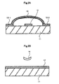
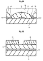
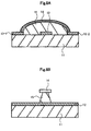
- FIG. 3A and 3B to FIGS. 9A and 9B are process views for describing a manufacturing method of the high-frequency semiconductor device having such a structure as described above.
- the respective views appended with A are sectional views taken along broken line X-X' of FIG. 1
- the respective views appended with B are sectional views taken along broken line Y-Y' of FIG. 1 .
- the following processes use processes in a standard MMIC manufacturing process.
- the first microstrip line 12 and the second microstrip lines 13-1, 13-2 are formed on a surface of the GaAs substrate 11 using the lift off method.
- the GaAs substrate 11 is exposed with a pattern mask formed with a reverse pattern of the line patterns forming each of the first microstrip line 12 and the second microstrip lines 13-1, 13-2. More specifically, the mask with reverse pattern enables to expose to line pattern portions only and to remove the resist layer from the exposed portion by etching.
- Au, Pt and Ti are evaporated to thicknesses of 500 nm, 100 nm and 1, 000 nm, respectively, for example, and then the whole of the GaAs substrate 11 is immersed into etching solution to peel off a metal evaporated layer except a targeted line pattern portion together with a resist layer using the lift off method to form the first microstrip line 12 and the second microstrip lines13-1, 13-2.
- a first resist layer 15 for forming the air bridge wiring 14 is applied over the whole surface of the substrate, and openings 17 for exposing the end portions of the second microstrip lines 13-1, 13-2 are formed as illustrated in FIGS. 4A and 4B by exposure using mask pattern and etching processing.
- a reverse pattern of the air bridge wiring 14 is formed on the second resist layer 16 as illustrated in FIGS. 5A and 5B by exposure and etching process.
- a conductive material for the air bridge wiring 14, such as Au is applied over the whole surface of the second resist layer 16 to a thickness of 1,000 nm as illustrated in FIG. 6B .
- the second resist layer 16 is subjected to the lift off method to form the air bridge wiring 14 as illustrated in FIGS. 7A and 7B .
- the first resist layer 15 still exists between the air bridge wiring 14 and the first microstrip line as illustrated in FIGS. 7A and 7B .
- FIGS. 8A and 8B illustrate a process for ashing with O 2 radical to remove the first resist layer 15 existing between the air bridge wiring 14 and the first microstrip line 12.
- ashing process is performed to remove the first resist layer 15. Since a thickness of the first resist layer 15 is approximately 3 ⁇ m, while a line width is approximately 10 ⁇ m, the first resist layer 15 is ashed starting from the edge side of the first microstrip line 12 and, the first resist layer 15 under the air bridge wiring 14 still remains even when the resist layer 15 on the peripheral is removed.
- the air bridge wiring 14 since the transverse cross section of the air bridge wiring 14 is in the form of a downward concave curvature, the air bridge wiring 14 has high resistance against bending force and can avoid coming into contact with the first microstrip line 12 even when some force toward the substrate 11 works on the air bridge wiring 14.
- the substrate temperature during ashing in the present embodiment is merely one example and, by controlling the temperature, the deflection degree of the wiring can be controlled, thus attaining a bridge shape having desirable mechanical strength.
Landscapes
- Internal Circuitry In Semiconductor Integrated Circuit Devices (AREA)
- Semiconductor Integrated Circuits (AREA)
Applications Claiming Priority (1)
| Application Number | Priority Date | Filing Date | Title |
|---|---|---|---|
| JP2007113430A JP5072417B2 (ja) | 2007-04-23 | 2007-04-23 | 半導体装置およびその製造方法 |
Publications (2)
| Publication Number | Publication Date |
|---|---|
| EP1986232A2 true EP1986232A2 (fr) | 2008-10-29 |
| EP1986232A3 EP1986232A3 (fr) | 2010-11-17 |
Family
ID=39666178
Family Applications (1)
| Application Number | Title | Priority Date | Filing Date |
|---|---|---|---|
| EP08154958A Withdrawn EP1986232A3 (fr) | 2007-04-23 | 2008-04-22 | Dispositif semi-conducteur et son procédé de fabrication |
Country Status (3)
| Country | Link |
|---|---|
| US (1) | US7812451B2 (fr) |
| EP (1) | EP1986232A3 (fr) |
| JP (1) | JP5072417B2 (fr) |
Cited By (1)
| Publication number | Priority date | Publication date | Assignee | Title |
|---|---|---|---|---|
| EP3869553A1 (fr) * | 2020-02-21 | 2021-08-25 | IQM Finland Oy | Pont pour établir des connexions sur puce supraconductrice et procédé de production de puces supraconductrices avec des ponts |
Families Citing this family (3)
| Publication number | Priority date | Publication date | Assignee | Title |
|---|---|---|---|---|
| JP5578012B2 (ja) | 2010-10-15 | 2014-08-27 | 三菱電機株式会社 | エアブリッジの製造方法 |
| US9263782B2 (en) * | 2013-01-23 | 2016-02-16 | Globalfoundries Inc. | Notch filter structure with open stubs in semiconductor substrate and design structure |
| KR102891999B1 (ko) | 2020-12-30 | 2025-12-01 | 삼성전자주식회사 | 삽입 손실을 줄이기 위한 전송 선로 구조 및 이를 포함하는 전자 장치 |
Citations (5)
| Publication number | Priority date | Publication date | Assignee | Title |
|---|---|---|---|---|
| JPH05152452A (ja) | 1991-11-27 | 1993-06-18 | Oki Electric Ind Co Ltd | エアブリツジ配線の形成方法 |
| JPH05218213A (ja) | 1992-01-31 | 1993-08-27 | Mitsubishi Electric Corp | 半導体装置及びその製造方法 |
| JPH0689940A (ja) | 1992-09-08 | 1994-03-29 | Mitsubishi Electric Corp | エアブリッジ配線構造 |
| JPH07135251A (ja) | 1993-11-11 | 1995-05-23 | Nippondenso Co Ltd | 高周波回路装置のエアブリッジ配線 |
| JP2007113430A (ja) | 2005-10-18 | 2007-05-10 | Sanden Corp | 斜板式圧縮機 |
Family Cites Families (14)
| Publication number | Priority date | Publication date | Assignee | Title |
|---|---|---|---|---|
| JPH01144656A (ja) * | 1987-11-30 | 1989-06-06 | Nec Corp | 多層配線構造およびその製造方法 |
| JP2569697B2 (ja) * | 1988-03-02 | 1997-01-08 | 三菱電機株式会社 | モノリシックマイクロ波集積回路の配線構造 |
| JPH0271520A (ja) * | 1988-09-07 | 1990-03-12 | Oki Electric Ind Co Ltd | レジストの除去方法 |
| JPH04109604A (ja) * | 1990-08-30 | 1992-04-10 | Sumitomo Electric Ind Ltd | マイクロ波半導体装置 |
| JPH04268750A (ja) * | 1991-02-25 | 1992-09-24 | Toshiba Corp | 半導体集積回路 |
| JP3116325B2 (ja) * | 1991-10-21 | 2000-12-11 | 日本電信電話株式会社 | 配線構体の製法 |
| US5408742A (en) * | 1991-10-28 | 1995-04-25 | Martin Marietta Corporation | Process for making air bridges for integrated circuits |
| US5561085A (en) | 1994-12-19 | 1996-10-01 | Martin Marietta Corporation | Structure for protecting air bridges on semiconductor chips from damage |
| JP3359780B2 (ja) * | 1995-04-12 | 2002-12-24 | 三菱電機株式会社 | 配線装置 |
| TW308719B (fr) * | 1995-10-23 | 1997-06-21 | Dow Corning | |
| US5686743A (en) * | 1996-07-10 | 1997-11-11 | Trw Inc. | Method of forming airbridged metallization for integrated circuit fabrication |
| US6261934B1 (en) * | 1998-03-31 | 2001-07-17 | Texas Instruments Incorporated | Dry etch process for small-geometry metal gates over thin gate dielectric |
| JP3450713B2 (ja) * | 1998-07-21 | 2003-09-29 | 富士通カンタムデバイス株式会社 | 半導体装置およびその製造方法、マイクロストリップ線路の製造方法 |
| JP3600544B2 (ja) * | 2001-03-30 | 2004-12-15 | ユーディナデバイス株式会社 | 半導体装置の製造方法 |
-
2007
- 2007-04-23 JP JP2007113430A patent/JP5072417B2/ja not_active Expired - Fee Related
-
2008
- 2008-04-22 EP EP08154958A patent/EP1986232A3/fr not_active Withdrawn
- 2008-04-22 US US12/107,391 patent/US7812451B2/en not_active Expired - Fee Related
Patent Citations (5)
| Publication number | Priority date | Publication date | Assignee | Title |
|---|---|---|---|---|
| JPH05152452A (ja) | 1991-11-27 | 1993-06-18 | Oki Electric Ind Co Ltd | エアブリツジ配線の形成方法 |
| JPH05218213A (ja) | 1992-01-31 | 1993-08-27 | Mitsubishi Electric Corp | 半導体装置及びその製造方法 |
| JPH0689940A (ja) | 1992-09-08 | 1994-03-29 | Mitsubishi Electric Corp | エアブリッジ配線構造 |
| JPH07135251A (ja) | 1993-11-11 | 1995-05-23 | Nippondenso Co Ltd | 高周波回路装置のエアブリッジ配線 |
| JP2007113430A (ja) | 2005-10-18 | 2007-05-10 | Sanden Corp | 斜板式圧縮機 |
Cited By (2)
| Publication number | Priority date | Publication date | Assignee | Title |
|---|---|---|---|---|
| EP3869553A1 (fr) * | 2020-02-21 | 2021-08-25 | IQM Finland Oy | Pont pour établir des connexions sur puce supraconductrice et procédé de production de puces supraconductrices avec des ponts |
| US11605586B2 (en) | 2020-02-21 | 2023-03-14 | Iqm Finland Oy | Airbridge for making connections on superconducting chip, and method for producing superconducting chips with airbridges |
Also Published As
| Publication number | Publication date |
|---|---|
| EP1986232A3 (fr) | 2010-11-17 |
| JP2008270617A (ja) | 2008-11-06 |
| JP5072417B2 (ja) | 2012-11-14 |
| US7812451B2 (en) | 2010-10-12 |
| US20080258311A1 (en) | 2008-10-23 |
Similar Documents
| Publication | Publication Date | Title |
|---|---|---|
| CN113826235B (zh) | 用于制造具有承载基底的显示器的方法、根据该方法制造的承载基底和确定用于柔性的显示器的覆盖玻璃 | |
| KR100922704B1 (ko) | 반도체 전력 소자 | |
| US6221750B1 (en) | Fabrication of deformable leads of microelectronic elements | |
| US20170018440A1 (en) | Robust multi-layer wiring elements and assemblies with embedded microelectronic elements | |
| EP0818816B1 (fr) | Méthode de fabrication des interconnexions du type pont pour les circuits intégrés | |
| JPH02257643A (ja) | 半導体装置及びその製造方法 | |
| EP0725445A1 (fr) | Transistor à effet de champ en forme de peigne | |
| US7812451B2 (en) | Semiconductor device and method of manufacturing the same | |
| DE112019006862B4 (de) | Piezoelektrisches Bauelement | |
| TW200929475A (en) | Interposer and method for manufacturing interposer | |
| JP2964981B2 (ja) | 半導体装置 | |
| TWI760712B (zh) | 半導體裝置及半導體裝置之製造方法 | |
| KR20090084710A (ko) | 배선 회로 기판 및 그 제조 방법 | |
| CN109427729B (zh) | 半导体装置封装和其制造方法 | |
| JP2008541436A (ja) | 金属層の応力を低減した半導体デバイス | |
| JPS6271256A (ja) | 化合物半導体集積回路 | |
| JPH1012722A (ja) | 半導体装置 | |
| EP1696481B1 (fr) | Procédé d'intégration d'un dispositif électronique dans une cavité d'un substrat | |
| JPH1022236A (ja) | 半導体装置およびその製造方法 | |
| US5331733A (en) | Method for manufacturing a connection device for a semiconductor device | |
| JP2797929B2 (ja) | 半導体装置 | |
| JPS62137853A (ja) | 多層配線の形成方法 | |
| CN119028944A (zh) | 一种晶圆结构及其形成方法 | |
| JP2004303784A (ja) | 半導体装置の製造方法 | |
| KR0161424B1 (ko) | 고집적 반도체소자의 배선층 |
Legal Events
| Date | Code | Title | Description |
|---|---|---|---|
| PUAI | Public reference made under article 153(3) epc to a published international application that has entered the european phase |
Free format text: ORIGINAL CODE: 0009012 |
|
| 17P | Request for examination filed |
Effective date: 20080422 |
|
| AK | Designated contracting states |
Kind code of ref document: A2 Designated state(s): AT BE BG CH CY CZ DE DK EE ES FI FR GB GR HR HU IE IS IT LI LT LU LV MC MT NL NO PL PT RO SE SI SK TR |
|
| AX | Request for extension of the european patent |
Extension state: AL BA MK RS |
|
| PUAL | Search report despatched |
Free format text: ORIGINAL CODE: 0009013 |
|
| AK | Designated contracting states |
Kind code of ref document: A3 Designated state(s): AT BE BG CH CY CZ DE DK EE ES FI FR GB GR HR HU IE IS IT LI LT LU LV MC MT NL NO PL PT RO SE SI SK TR |
|
| AX | Request for extension of the european patent |
Extension state: AL BA MK RS |
|
| REG | Reference to a national code |
Ref country code: DE Ref legal event code: R108 |
|
| AKX | Designation fees paid |
Designated state(s): FR |
|
| REG | Reference to a national code |
Ref country code: DE Ref legal event code: R108 Effective date: 20110714 |
|
| 17Q | First examination report despatched |
Effective date: 20130405 |
|
| STAA | Information on the status of an ep patent application or granted ep patent |
Free format text: STATUS: THE APPLICATION IS DEEMED TO BE WITHDRAWN |
|
| 18D | Application deemed to be withdrawn |
Effective date: 20161101 |