EP1983640B1 - Power conversion apparatus and method of estimating power cycle life - Google Patents
Power conversion apparatus and method of estimating power cycle life Download PDFInfo
- Publication number
- EP1983640B1 EP1983640B1 EP08250680A EP08250680A EP1983640B1 EP 1983640 B1 EP1983640 B1 EP 1983640B1 EP 08250680 A EP08250680 A EP 08250680A EP 08250680 A EP08250680 A EP 08250680A EP 1983640 B1 EP1983640 B1 EP 1983640B1
- Authority
- EP
- European Patent Office
- Prior art keywords
- power
- temperature
- conversion apparatus
- power conversion
- power semiconductor
- Prior art date
- Legal status (The legal status is an assumption and is not a legal conclusion. Google has not performed a legal analysis and makes no representation as to the accuracy of the status listed.)
- Ceased
Links
Images



Classifications
-
- H—ELECTRICITY
- H02—GENERATION; CONVERSION OR DISTRIBUTION OF ELECTRIC POWER
- H02M—APPARATUS FOR CONVERSION BETWEEN AC AND AC, BETWEEN AC AND DC, OR BETWEEN DC AND DC, AND FOR USE WITH MAINS OR SIMILAR POWER SUPPLY SYSTEMS; CONVERSION OF DC OR AC INPUT POWER INTO SURGE OUTPUT POWER; CONTROL OR REGULATION THEREOF
- H02M5/00—Conversion of AC power input into AC power output, e.g. for change of voltage, for change of frequency, for change of number of phases
- H02M5/40—Conversion of AC power input into AC power output, e.g. for change of voltage, for change of frequency, for change of number of phases with intermediate conversion into DC
- H02M5/42—Conversion of AC power input into AC power output, e.g. for change of voltage, for change of frequency, for change of number of phases with intermediate conversion into DC by static converters
- H02M5/44—Conversion of AC power input into AC power output, e.g. for change of voltage, for change of frequency, for change of number of phases with intermediate conversion into DC by static converters using discharge tubes or semiconductor devices to convert the intermediate DC into AC
- H02M5/443—Conversion of AC power input into AC power output, e.g. for change of voltage, for change of frequency, for change of number of phases with intermediate conversion into DC by static converters using discharge tubes or semiconductor devices to convert the intermediate DC into AC using devices of a thyratron or thyristor type requiring extinguishing means
- H02M5/45—Conversion of AC power input into AC power output, e.g. for change of voltage, for change of frequency, for change of number of phases with intermediate conversion into DC by static converters using discharge tubes or semiconductor devices to convert the intermediate DC into AC using devices of a thyratron or thyristor type requiring extinguishing means using semiconductor devices only
- H02M5/451—Conversion of AC power input into AC power output, e.g. for change of voltage, for change of frequency, for change of number of phases with intermediate conversion into DC by static converters using discharge tubes or semiconductor devices to convert the intermediate DC into AC using devices of a thyratron or thyristor type requiring extinguishing means using semiconductor devices only with automatic control of output voltage or frequency
-
- G—PHYSICS
- G01—MEASURING; TESTING
- G01R—MEASURING ELECTRIC VARIABLES; MEASURING MAGNETIC VARIABLES
- G01R31/00—Arrangements for testing electric properties; Arrangements for locating electric faults; Arrangements for electrical testing characterised by what is being tested not provided for elsewhere
- G01R31/26—Testing of individual semiconductor devices
-
- G—PHYSICS
- G01—MEASURING; TESTING
- G01R—MEASURING ELECTRIC VARIABLES; MEASURING MAGNETIC VARIABLES
- G01R31/00—Arrangements for testing electric properties; Arrangements for locating electric faults; Arrangements for electrical testing characterised by what is being tested not provided for elsewhere
- G01R31/327—Testing of circuit interrupters, switches or circuit-breakers
-
- H—ELECTRICITY
- H02—GENERATION; CONVERSION OR DISTRIBUTION OF ELECTRIC POWER
- H02M—APPARATUS FOR CONVERSION BETWEEN AC AND AC, BETWEEN AC AND DC, OR BETWEEN DC AND DC, AND FOR USE WITH MAINS OR SIMILAR POWER SUPPLY SYSTEMS; CONVERSION OF DC OR AC INPUT POWER INTO SURGE OUTPUT POWER; CONTROL OR REGULATION THEREOF
- H02M7/00—Conversion of AC power input into DC power output; Conversion of DC power input into AC power output
- H02M7/42—Conversion of DC power input into AC power output without possibility of reversal
- H02M7/44—Conversion of DC power input into AC power output without possibility of reversal by static converters
- H02M7/48—Conversion of DC power input into AC power output without possibility of reversal by static converters using discharge tubes with control electrode or semiconductor devices with control electrode
Definitions
- An inverter a power conversion apparatus, has found a wide range of applications as a motor speed controller in industrial fields and also with household appliances. Since power semiconductors in the power conversion apparatus generate large losses, the inverter employs a structure that dissipates heat caused by the losses. That is, it has cooling fins and cooling fans so that heat from the power semiconductors as a heat source is transmitted to the cooling fins that in turn exchange heat with air blown to the cooling fins from the cooling fan, thus dissipating heat by an air-cooling method.
- a so-called power cycle is repeated in which a junction temperature Tj of a chip in a power semiconductor that generates large losses changes from an elevated temperature state (the junction temperature of the silicon chip rises during the operation of the apparatus) to an intermediate temperature state (the junction temperature of the silicon chip lowers while the apparatus is at rest) and to an elevated temperature state (the junction temperature of the silicon chip rises during the operation of the apparatus) again.
- a phenomenon is commonly observed in which the power semiconductors fail due to thermal fatigue according to their power cycle longevity.
- Power semiconductors are formed of materials with different thermal expansion coefficients (such as silicon chip, copper heat dissipating plate, plastic case and silicon gel), so repetition of thermal expansion and contraction causes thermal stresses in these materials, resulting in disconnection of aluminum bonding wires and cracks in solder, which in turn leads to destruction of the power semiconductors. This phenomenon is called a power cycle.
- thermal expansion coefficients such as silicon chip, copper heat dissipating plate, plastic case and silicon gel
- JP-A-3-261877 discloses a technique that involves estimating a junction temperature of a power semiconductor from an electric current and a temperature of a cooling fin, estimating a degree of fatigue of the power semiconductor using the estimated junction temperature and a power semiconductor operation history calculation means, and displaying a longevity of the power semiconductor when the estimated fatigue value exceeds a predetermined value.
- JP-A-7-135731 discloses a technique that involves estimating a junction temperature of a power semiconductor from an electric current, voltage and temperature of a cooling fin, estimating a degree of fatigue of the power semiconductor from the estimated junction temperature, and turning off the power semiconductor when the estimated fatigue value exceeds a predetermined value.
- JP-A-8-51768 discloses a technique that involves entering a difference between junction temperatures when an inverter is in operation and at rest, estimating a degree of fatigue of the power semiconductor from a power cycle longevity curve, and turning off the power semiconductor when the estimated fatigue value exceeds a predetermined value.
- JP-A-2006-254574 discloses a technique that involves estimating a junction temperature difference of a power semiconductor from an output frequency command value and an output current value and, from a power cycle longevity curve, displaying a remaining percentage of the power cycle longevity of the power semiconductor.
- estimating the junction temperature of a power semiconductor allows the estimation of the degree of fatigue of the power semiconductor and therefore the longevity of power semiconductor parts.
- a so-called power cycle is repeated in which a junction temperature Tj of a chip in a power semiconductor that generates large losses changes from an elevated temperature state (the junction temperature of the silicon chip rises during the operation of the apparatus) to an intermediate temperature state (the junction temperature of the silicon chip decreases while the apparatus is at rest) and to an elevated temperature state (the junction temperature of the silicon chip rises during the operation of the apparatus) again.
- a phenomenon is commonly observed in which the power semiconductors fail due to thermal fatigue according to their power cycle longevity.
- the elevator may not operate. So, depending on the application, it is desired to be able to diagnose the power cycle longevity of the power semiconductor.
- the prior art warns of a fatigue of the power semiconductor two or three years after the facility has begun its service, so the operator can only know an imminent failure of the power semiconductor just before the actual occurrence of the failure. That is, during a test operation of a facility conducted at the time of its introduction, it is not possible to estimate the longevity of the power semiconductor from an actual operation pattern, leaving much to be desired in terms of ease of use on the part of the facility.
- JP-A-2006-166509 discloses an air conditioning apparatus in which the temperature of radiation fins are used in the calculation of the service life of the apparatus.
- a power conversion apparatus comprising:
- a power cycle longevity estimation method to determine a power cycle longevity of a power semiconductor installed in a power conversion circuit that supplies an ac power of variable voltage and variable frequency in a start/stop pattern in which start/stop actions are repeated, the power cycle longevity estimation method comprising the steps of:
- a more preferred configuration of the above power conversion apparatus is as follows:
- the power cycle longevity estimation method which diagnoses a power cycle longevity of a power semiconductor installed in a power conversion circuit that supplies an ac power of variable voltage and variable frequency, comprises the steps of: detecting a temperature of the power semiconductor; and calculating the power cycle longevity of the power semiconductor based on a maximum temperature rise determined from the detected temperatures of the power semiconductor.
- a power conversion apparatus and a power cycle longevity estimation method both able to improve the ease of use on the part of a facility, can be provided.
- Fig. 1 is a main circuit configuration diagram of a power conversion apparatus according to one embodiment of this invention.
- the power conversion circuit of this embodiment comprises a rectifier 1 to commutate an ac voltage of an ac power supply to transform it into a dc voltage, a smoothing capacitor 2 to smooth the dc voltage of the rectifier 1 and an inverter 3 to transform the dc voltage of the rectifier 1 into an ac voltage, and outputs a variable-voltage, variable-frequency ac power to an ac motor 4.
- Various control data in the power conversion apparatus of this embodiment can be set and changed from a digital operation panel 8.
- the digital operation panel 8 is provided with a display unit to display when an abnormal condition occurs.
- Power semiconductor modules in the rectifier 1 and the inverter 3 are mounted on cooling fins described later and are air-cooled by a cooling fan 6. A detailed configuration of the power semiconductor modules will be described later. Temperature sensors 7 are mounted on the cooling fins to detect temperatures of the power semiconductor modules in the rectifier 1 and the inverter 3.
- a temperature sensor 11 is installed inside the power semiconductor modules near silicon chips. These temperature sensors 7, 11 suitably use thermistors that change their resistance according to temperatures.
- the thermistor may be one that increases its resistance with a temperature or one that reduces it with an increasing temperature.
- a switching element, a power semiconductor, used in the inverter 3 is controlled by a microcomputer-based control circuit 5 which controls the entire power conversion apparatus. More specifically, the control circuit 5 is configured to be able to perform control processing according to various control data entered from the digital operation panel 8.
- Denoted 12 is a driver circuit that drives the switching element of the inverter 3.
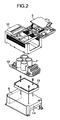
- Fig. 2 shows an example arrangement of main circuit parts.
- a composite module 13, or a collective power semiconductor, having the rectifier 1, the inverter 3 and the temperature sensor 7 installed in one module is mounted on a cooling fin 14, with a cooling fan 6 (shown dotted in the figure) for cooling the cooling fin 14 mounted on an upper surface of the cooling fin.
- the composite module 13 configured as a collective power semiconductor causes great losses resulting in heat.
- the heat produced by the losses is transferred to the cooling fin 14 which is cooled by the cooling fan 6.
- the cooling fan 6 therefore can protect the composite module 13 or the collective power semiconductor against being overheated.
- the power conversion apparatus may be configured so that when the temperature detected by the temperature sensor 7exceeds a preset temperature, the power conversion apparatus is made to stop and indicate an overheating of the power semiconductor.
- a chip inside a power semiconductor that generates large losses repetitively goes through a power cycle in which a junction temperature Tj of the chip changes from an elevated temperature state (the junction temperature of the silicon chip rises when the apparatus is in operation) to an intermediate temperature state (the junction temperature of the silicon chip decreases when the apparatus is at rest) and back again to an elevated temperature state (the junction temperature of the silicon chip rises when the apparatus is in operation).
- Tj of the chip changes from an elevated temperature state (the junction temperature of the silicon chip rises when the apparatus is in operation) to an intermediate temperature state (the junction temperature of the silicon chip decreases when the apparatus is at rest) and back again to an elevated temperature state (the junction temperature of the silicon chip rises when the apparatus is in operation).
- Fig. 3 shows an example of operation pattern of an elevator that frequently repeats start and stop.
- a detected temperature of the fin is one that is detected by the temperature sensor 7 mounted on the cooling fin of Fig. 1 .
- the elevator starts and reaches a destination floor, it stops.
- a junction temperature Tj of a chip inside the power semiconductor 9 that generates large losses in the power conversion apparatus changes from an elevated temperature state (during operation of the apparatus, the junction temperature of the silicon chip increases) to an intermediate temperature state (when the apparatus is at rest, the silicon chip junction temperature decreases) and back again to the elevated temperature state (the silicon chip junction temperature rises when the apparatus is in operation).
- the chip temperature in the power semiconductor 9 is forced to go through the so-called power cycle repetitively.
- a temperature Tc of the cooling fin that cools the power semiconductor by dissipating heat transmitted from the power semiconductor as a heat source naturally rises and falls in a certain relationship with the chip junction temperature Tj.
- Monitoring the detected temperature of the temperature sensor 7 on the cooling fin 14 installed near the power semiconductor 9 in this operation pattern makes it possible to predict the number of power cycles allowed in its service life in the operation pattern concerned.
- Tj Tc + Rjc * P ⁇ 1
- Rjc a thermal resistance between the junction and the case
- P1 a loss of the power semiconductor 9 in the operation pattern of the power conversion apparatus. This loss P1 can be expressed as follows.
- P ⁇ 1 Pon + Poff + Psat
- Pon is an on-loss that occurs when the power semiconductor 9 makes a transition from an off-state to an on-state
- Poff is an off-loss that occurs when the power semiconductor 9 changes its state from the on-state to the off-state
- Psat is a steady-state loss
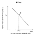
- Fig. 4 shows a power cycle longevity curve of the power semiconductor 9. This longevity curve is characteristic of the power semiconductor and is determined uniquely by a temperature increase of the power semiconductor, not by an ambient temperature of the power semiconductor.
- An elevator operation pattern cycle for the maximum temperature rise ⁇ Tc2 of the case needs to be determined.
- the number of longevity power cycles Nc2 for the maximum temperature rise ⁇ Tc2 is 1,000,000 cycles (intersection A in Fig. 4 ).
- the power semiconductor 9 will fail by thermal fatigue in as short as slightly more than one year after the elevator has begun its service, halting the operation of the elevator facility.
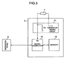
- Fig. 5 shows an embodiment of a method that is intended to overcome the aforementioned problem and which predicts during a test operation of a facility when a power semiconductor in a power conversion apparatus will fail due to a thermal fatigue according to its power cycle longevity.
- Fig. 6 is a flow chart of this embodiment for the above operation pattern.
- an operator selects a test operation mode on the digital operation panel 8 mounted on the power conversion apparatus during a facility test operation (step 61) and enters into a test operation mode column the number of start/stop actions repeated in a unit time of the test operation M, service hours in a day H and the number of service days in a year D (step 62).
- a test operation mode it is also possible to store a plurality of representative operation patterns in a memory means in advance and select a desired one from among them. Or with these representative operation patterns displayed, an operator may set M, H and D by adjusting the displayed operation pattern.
- the test operation is started (step 63) and the start/stop actions are repetitively performed (step 68). At this time, a signal of the temperature sensor 7 installed near the power semiconductor is transmitted to the microcomputer 15 through the temperature sensing circuit 17.
- the temperature sensor 7 is a thermistor. A temperature characteristic of the thermistor used will be explained by taking up an example case where its resistance decreases with an increasing temperature.
- R25 is a thermistor resistance at a temperature of 25°C
- B is a constant.
- the microcomputer calculates the temperature T in real time from the equation (1).
- equation (1) is complex to calculate, it is possible to determine from the equation (1) data representing a correlation between the input voltage at the analog port terminal AD proportional to the thermistor resistance and the thermistor temperature, store the data in a nonvolatile memory 16 as table data in advance, and then call up the thermistor temperature T from the table data.
- a test operation is started in the most stringent operation pattern to calculate a temperature increase ⁇ Tc1 of the power semiconductor 9 in a start/stop period or operation period ⁇ t1 shown in Fig. 3 and also a temperature increase ⁇ Tc2 of the power semiconductor 9 in the next start/stop period ⁇ t2 (step 64) and hold them (step 65).
- Temperature increases ⁇ Tcn of the power semiconductor 9 during start/stop periods ⁇ tn are calculated successively and the largest ⁇ Tcj of these temperature increases ⁇ Tcn is held (steps 66, 67).
- Only the first temperature increase ⁇ Tc1 may be excluded from the largest temperature increase ⁇ Tcj. That is, the largest temperature increase ⁇ Tcj may be picked up and held from among the temperature increases that include the temperature increase ⁇ Tc2 and subsequent ones.
- the composite module 13 has an IGBT chip that constitutes the inverter 3.
- a temperature characteristic of the IGBT is a positive feedback.
- V CEsat a voltage between the chip's collector and emitter
- the temperature characteristic of the IGBT chip is of a negative feedback (as the chip temperature rises, the chip's collector-emitter voltage V CEsat decreases).
- This temperature characteristic is a design philosophy at the design stage of the IGBT chip.
- the first temperature rise ⁇ Tc1 during the test operation in which the chip temperature is equal to an ambient temperature, cannot be the largest among the temperature rises ⁇ Tcn.
- the number of longevity power cycles Nj corresponding to the temperature increase ⁇ Tcj is read out from the power cycle longevity curve data stored in advance in the nonvolatile memory.
- the power cycle longevity in years Y of the power semiconductor 9 under the above operation pattern condition is calculated from the equation shown below (step 70).
- Y ⁇ * Nj / M * H * D
- ⁇ is a safety factor ( ⁇ 1) that can be set and entered from the digital operation panel 8.
- the calculated longevity in years is displayed on a display unit of the digital operation panel 8 (step 71).
- the temperature increase ⁇ Tcj can also be displayed on the display unit of the digital operation panel 8.
- the above procedure makes it possible to check during a test operation of a facility whether or not the capacity of the power conversion apparatus installed in the facility is correctly chosen.
- the number of start/stop actions may be set for a period of one minute, rather than an hour.
- the calculated longevity in years displayed on the operation panel 8 is less than a preset target longevity (for example, 10 years), some measures to cover the target longevity may be taken during the test operation of the facility.
- a preset target longevity for example, 10 years
- the power cycle longevity in years Y of the power semiconductor 9 is determined again in the test operation mode and then further measures to cover the target longevity need to be taken.
- the power cycle longevity of the power semiconductor can be diagnosed during the test operation of the facility by using a temperature of the power semiconductor in the power conversion apparatus as detected by a temperature sensing circuit and a power cycle longevity curve of the power semiconductor, it can be easily determined when, after the facility enters into service, the power semiconductor or the power conversion apparatus itself needs to be replaced.
- the power cycle longevity can be diagnosed during the test operation of the facility, it is possible to know in advance during the test operation whether or not a failure caused by thermal fatigue according to the power cycle longevity of the power semiconductor will occur in a relatively short period of time after the facility enters into service.
- This embodiment allows an operation condition or operation pattern of a power conversion apparatus to be set and entered from the operation panel and also allows the use of a temperature of the power semiconductor as detected by the temperature sensing circuit under the operation condition and of a power cycle longevity curve of the power semiconductor.
- this embodiment can estimate during a test operation of a facility the fatigue longevity of a power semiconductor, making it possible to check during the test operation whether or not a failure due to thermal fatigue according to the power cycle longevity will occur in a relatively short period of time after the facility enters into operation.
- a check can be made, during the test operation of a facility, as to an appropriateness in the selection of a capacity of the power conversion apparatus, an operator, when the facility enters into service, can be relieved of an apprehension of a possible failure. This produces effects of improving the ease of use of the facility and of greatly reducing a down time of the facility.
Landscapes
- Engineering & Computer Science (AREA)
- Power Engineering (AREA)
- Physics & Mathematics (AREA)
- General Physics & Mathematics (AREA)
- Inverter Devices (AREA)
- Power Conversion In General (AREA)
- Testing Of Individual Semiconductor Devices (AREA)
Applications Claiming Priority (1)
| Application Number | Priority Date | Filing Date | Title |
|---|---|---|---|
| JP2007111192A JP5016967B2 (ja) | 2007-04-20 | 2007-04-20 | 電力変換装置及びパワーサイクル寿命予測方法 |
Publications (3)
| Publication Number | Publication Date |
|---|---|
| EP1983640A2 EP1983640A2 (en) | 2008-10-22 |
| EP1983640A3 EP1983640A3 (en) | 2011-01-12 |
| EP1983640B1 true EP1983640B1 (en) | 2012-04-11 |
Family
ID=39674853
Family Applications (1)
| Application Number | Title | Priority Date | Filing Date |
|---|---|---|---|
| EP08250680A Ceased EP1983640B1 (en) | 2007-04-20 | 2008-02-28 | Power conversion apparatus and method of estimating power cycle life |
Country Status (6)
| Country | Link |
|---|---|
| US (1) | US7904254B2 (cg-RX-API-DMAC7.html) |
| EP (1) | EP1983640B1 (cg-RX-API-DMAC7.html) |
| JP (2) | JP5016967B2 (cg-RX-API-DMAC7.html) |
| KR (1) | KR100937806B1 (cg-RX-API-DMAC7.html) |
| CN (1) | CN101299577A (cg-RX-API-DMAC7.html) |
| TW (1) | TW200843316A (cg-RX-API-DMAC7.html) |
Families Citing this family (39)
| Publication number | Priority date | Publication date | Assignee | Title |
|---|---|---|---|---|
| JP5586866B2 (ja) * | 2008-09-29 | 2014-09-10 | 株式会社日立産機システム | 電力変換装置 |
| JP5476718B2 (ja) * | 2009-01-13 | 2014-04-23 | 日産自動車株式会社 | 電力用半導体モジュールの安全装置 |
| JP2011026065A (ja) * | 2009-07-24 | 2011-02-10 | Hitachi Ltd | エレベータ制御装置 |
| DE102009055055A1 (de) * | 2009-12-21 | 2011-06-22 | Robert Bosch GmbH, 70469 | Verfahren zur Fehlererkennung bei einer durch einen Wechselrichter angesteuerten elektrischen Maschine in einem Kraftfahrzeug und Vorrichtung zur Überwachung eines Betriebs der elektrischen Maschine |
| US8829838B2 (en) | 2010-03-10 | 2014-09-09 | Hitachi, Ltd. | Power converter |
| ES2396533B1 (es) * | 2010-04-13 | 2014-01-27 | Gamesa Innovation & Technology, S.L. | Métodos de monitorización de la salud de dispositivos semiconductores. |
| US8471516B2 (en) * | 2010-05-24 | 2013-06-25 | Rockwell Automation Technologies, Inc. | Adjustable speed drive lifetime improvement method |
| US8736091B2 (en) | 2010-06-18 | 2014-05-27 | Rockwell Automation Technologies, Inc. | Converter lifetime improvement method for doubly fed induction generator |
| TWI417746B (zh) | 2010-12-03 | 2013-12-01 | Ind Tech Res Inst | 裝置的效能預測及故障檢測之方法 |
| JP5437989B2 (ja) * | 2010-12-22 | 2014-03-12 | 株式会社日立製作所 | エレベータ制御システム |
| EP2568268A1 (en) | 2011-09-07 | 2013-03-13 | kk-electronic a/s | Method for estimating the temperature of a semiconductor chip |
| CN102590726B (zh) * | 2012-02-23 | 2014-01-08 | 北京航空航天大学 | 一种评估功率vmos管寿命以及可靠性的分析方法 |
| DE102012106033A1 (de) * | 2012-07-05 | 2014-01-09 | Halla Visteon Climate Control Corporation 95 | Verfahren zum Betreiben eines Inverters eines elektrischen Kältemittelverdichters unter Verwendung von elektrolytischen Zwischenkreis-Kondensatoren |
| CN104736981B (zh) * | 2012-12-12 | 2017-12-22 | 富士电机株式会社 | 半导体芯片温度推定装置及过热保护装置 |
| US10379070B2 (en) * | 2013-03-15 | 2019-08-13 | Mitsubishi Electric Corporation | Power module |
| CN104182015B (zh) * | 2013-05-23 | 2018-04-27 | 联想(北京)有限公司 | 一种信息处理的方法及一种电子设备 |
| JP6082664B2 (ja) * | 2013-06-19 | 2017-02-15 | 株式会社日立産機システム | 電力変換装置 |
| JP5907236B2 (ja) * | 2013-12-11 | 2016-04-26 | 株式会社デンソー | 温度検出装置 |
| US10067483B1 (en) | 2014-08-28 | 2018-09-04 | Apple Inc. | Controlling electrical device based on temperature and voltage |
| CN104251965B (zh) * | 2014-09-24 | 2017-07-04 | 河北工业大学 | 一种igbt动态性能测试装置及其运行方法 |
| JP6191586B2 (ja) * | 2014-12-02 | 2017-09-06 | トヨタ自動車株式会社 | モータコントローラ、電動車両、及び、スイッチング素子の熱ストレス推定方法 |
| US9652008B2 (en) * | 2015-04-02 | 2017-05-16 | Det International Holding Limited | Power module |
| EP3109649B1 (en) * | 2015-06-25 | 2019-08-07 | ABB Schweiz AG | Aging determination of power semiconductor device in electric drive system |
| EP3118638B1 (en) | 2015-06-25 | 2019-08-07 | ABB Schweiz AG | Temperature estimation in power semiconductor device in electric drive system |
| JP6010204B1 (ja) * | 2015-10-26 | 2016-10-19 | ファナック株式会社 | パワー素子の予測寿命を学習する機械学習装置及び方法並びに該機械学習装置を備えた寿命予測装置及びモータ駆動装置 |
| WO2017183102A1 (ja) * | 2016-04-19 | 2017-10-26 | 株式会社日立産機システム | 電力変換装置 |
| CN108549001B (zh) * | 2018-02-02 | 2021-10-12 | 上海大学 | 一种电力电子模块劳损状态的检测系统及方法 |
| JP6958499B2 (ja) * | 2018-07-09 | 2021-11-02 | 三菱電機株式会社 | 半導体装置および電力変換装置 |
| JP7118019B2 (ja) * | 2019-02-05 | 2022-08-15 | 三菱電機株式会社 | 半導体モジュール、および半導体モジュールの寿命予測システム |
| CN109814020B (zh) * | 2019-03-05 | 2024-11-01 | 润新微电子(大连)有限公司 | 功率半导体器件功率循环测试系统 |
| US10742149B1 (en) * | 2019-04-22 | 2020-08-11 | General Electric Company | System and method for reactive power control of a wind turbine by varying switching frequency of rotor side converter |
| JP7472663B2 (ja) * | 2020-06-05 | 2024-04-23 | 富士電機株式会社 | 電力変換装置 |
| CN112098789B (zh) * | 2020-08-04 | 2023-06-13 | 株洲中车时代半导体有限公司 | Igbt模块寿命的统计方法、装置、电子设备及存储介质 |
| US12560632B2 (en) * | 2020-08-28 | 2026-02-24 | Tmeic Corporation | State estimation system and state estimation method for power conversion semiconductor apparatus |
| EP4053525B1 (en) * | 2021-03-01 | 2023-08-09 | Mitsubishi Electric R&D Centre Europe B.V. | Process for monitoring the thermal resistance between a power semiconductor and its heat sink terminal |
| CN113595142B (zh) * | 2021-08-24 | 2023-09-12 | 华北电力大学(保定) | 一种考虑光伏组件配置和功率跟踪限值影响的光伏逆变器寿命评估方法 |
| CN116776747B (zh) * | 2023-08-18 | 2023-11-03 | 江西五十铃汽车有限公司 | 一种igbt模块使用寿命计算方法及系统 |
| JP2025030457A (ja) * | 2023-08-23 | 2025-03-07 | 株式会社日立産機システム | 電力変換装置および電力変換方法 |
| JP2025077055A (ja) | 2023-11-03 | 2025-05-19 | 株式会社Soken | リユース可否判定装置及びリユース可否判定方法 |
Family Cites Families (20)
| Publication number | Priority date | Publication date | Assignee | Title |
|---|---|---|---|---|
| US3237448A (en) * | 1960-06-16 | 1966-03-01 | Howell Instruments | Equivalent operating time apparatus |
| GB1104141A (en) * | 1964-04-24 | 1968-02-21 | Smiths Industries Ltd | Improvements in or relating to electrical apparatus for providing a representation of engine-life |
| JP2767965B2 (ja) * | 1990-03-12 | 1998-06-25 | 三菱電機株式会社 | 電力変換装置及びインバータ装置 |
| JP3139871B2 (ja) * | 1993-03-17 | 2001-03-05 | 株式会社東芝 | 自動車用半導体電力変換装置 |
| JPH07135731A (ja) | 1993-11-09 | 1995-05-23 | Fuji Electric Co Ltd | 半導体素子の過熱保護装置 |
| JP3209004B2 (ja) | 1994-08-10 | 2001-09-17 | 株式会社明電舎 | パワースイッチング素子の寿命監視装置及び同寿命監視装置を有するパワースイッチング素子を用いた装置 |
| JP2001204177A (ja) * | 2000-01-18 | 2001-07-27 | Miyachi Technos Corp | 金属部材接合用又はリフローハンダ付用の交流波形インバータ式電源装置 |
| JP2002101668A (ja) * | 2000-09-26 | 2002-04-05 | Meidensha Corp | 半導体電力変換装置の寿命推定方法および半導体電力変換装置 |
| JP3818082B2 (ja) | 2001-04-26 | 2006-09-06 | 株式会社明電舎 | インバータ |
| JP3788334B2 (ja) * | 2001-12-05 | 2006-06-21 | オムロン株式会社 | 半導体装置の異常検出装置 |
| KR100661107B1 (ko) * | 2003-03-12 | 2006-12-26 | 미쓰비시덴키 가부시키가이샤 | 전동기 제어장치 |
| JP4366269B2 (ja) | 2004-07-30 | 2009-11-18 | 株式会社日立産機システム | 半導体素子の温度検出方法及び電力変換装置 |
| JP2005252090A (ja) | 2004-03-05 | 2005-09-15 | Hitachi Industrial Equipment Systems Co Ltd | 半導体素子の温度検出方法及び電力変換装置 |
| TW200530566A (en) | 2004-03-05 | 2005-09-16 | Hitachi Ind Equipment Sys | Method for detecting temperature of semiconductor element and semiconductor power converter |
| FI118363B (fi) * | 2004-03-29 | 2007-10-15 | Vacon Oyj | Tehopuolijohdekomponenttien suojaus |
| JP2005354812A (ja) * | 2004-06-11 | 2005-12-22 | Hitachi Ltd | インバータ装置 |
| JP2006166569A (ja) * | 2004-12-06 | 2006-06-22 | Daikin Ind Ltd | 空気調和装置 |
| JP2006254574A (ja) | 2005-03-09 | 2006-09-21 | Yaskawa Electric Corp | インバータの保護装置 |
| JP4591246B2 (ja) * | 2005-07-14 | 2010-12-01 | 株式会社日立製作所 | 電力変換器 |
| KR100747228B1 (ko) * | 2006-04-28 | 2007-08-07 | 현대자동차주식회사 | 모터 구속시 인버터 내 전력소자 보호 방법 |
-
2007
- 2007-04-20 JP JP2007111192A patent/JP5016967B2/ja not_active Expired - Fee Related
-
2008
- 2008-02-21 KR KR1020080015762A patent/KR100937806B1/ko not_active Expired - Fee Related
- 2008-02-28 EP EP08250680A patent/EP1983640B1/en not_active Ceased
- 2008-02-29 US US12/039,979 patent/US7904254B2/en active Active
- 2008-02-29 TW TW097107072A patent/TW200843316A/zh not_active IP Right Cessation
- 2008-03-14 CN CNA2008100860873A patent/CN101299577A/zh active Pending
-
2012
- 2012-06-08 JP JP2012130383A patent/JP5452663B2/ja not_active Expired - Fee Related
Also Published As
| Publication number | Publication date |
|---|---|
| US20080262750A1 (en) | 2008-10-23 |
| KR20080094550A (ko) | 2008-10-23 |
| US7904254B2 (en) | 2011-03-08 |
| JP2008271703A (ja) | 2008-11-06 |
| KR100937806B1 (ko) | 2010-01-20 |
| EP1983640A3 (en) | 2011-01-12 |
| JP5016967B2 (ja) | 2012-09-05 |
| TW200843316A (en) | 2008-11-01 |
| JP2012191849A (ja) | 2012-10-04 |
| EP1983640A2 (en) | 2008-10-22 |
| TWI364157B (cg-RX-API-DMAC7.html) | 2012-05-11 |
| JP5452663B2 (ja) | 2014-03-26 |
| CN101299577A (zh) | 2008-11-05 |
Similar Documents
| Publication | Publication Date | Title |
|---|---|---|
| US7904254B2 (en) | Power conversion apparatus and method of estimating power cycle life | |
| JP4367339B2 (ja) | 電動機制御装置 | |
| US6724313B2 (en) | Fault detection system | |
| JP4591246B2 (ja) | 電力変換器 | |
| JP3541460B2 (ja) | インバータ装置 | |
| WO2019049399A1 (ja) | 電力変換装置、電動機制御システム、および電力変換装置の診断方法 | |
| JP2002101668A (ja) | 半導体電力変換装置の寿命推定方法および半導体電力変換装置 | |
| US11846668B2 (en) | Method for assessing the thermal loading of a converter | |
| CN112305336A (zh) | 基于运行状况检测功率模块的故障 | |
| TWI785692B (zh) | 電力轉換裝置及遠距監視系統 | |
| JP2008206217A (ja) | 半導体スイッチング素子の寿命監視回路を有する半導体電力変換装置 | |
| JP5476718B2 (ja) | 電力用半導体モジュールの安全装置 | |
| CN106679076A (zh) | 变频器功率模块温度控制方法和控制装置 | |
| JP2013172540A (ja) | 電力変換装置 | |
| JP2007312536A (ja) | インバータ装置 | |
| JP7472663B2 (ja) | 電力変換装置 | |
| JP2025043991A (ja) | 電力変換装置、電力変換装置の遠隔監視システム及び電力変換装置の寿命推定方法 | |
| CN118671467A (zh) | 用于计算电换流器的剩余循环寿命的方法和用于执行该方法的电换流器 | |
| JP2021197844A (ja) | 無停電電源装置及び無停電電源装置の制御方法 |
Legal Events
| Date | Code | Title | Description |
|---|---|---|---|
| PUAI | Public reference made under article 153(3) epc to a published international application that has entered the european phase |
Free format text: ORIGINAL CODE: 0009012 |
|
| 17P | Request for examination filed |
Effective date: 20080314 |
|
| AK | Designated contracting states |
Kind code of ref document: A2 Designated state(s): AT BE BG CH CY CZ DE DK EE ES FI FR GB GR HR HU IE IS IT LI LT LU LV MC MT NL NO PL PT RO SE SI SK TR |
|
| AX | Request for extension of the european patent |
Extension state: AL BA MK RS |
|
| PUAL | Search report despatched |
Free format text: ORIGINAL CODE: 0009013 |
|
| AK | Designated contracting states |
Kind code of ref document: A3 Designated state(s): AT BE BG CH CY CZ DE DK EE ES FI FR GB GR HR HU IE IS IT LI LT LU LV MC MT NL NO PL PT RO SE SI SK TR |
|
| AX | Request for extension of the european patent |
Extension state: AL BA MK RS |
|
| AKX | Designation fees paid |
Designated state(s): DE FR GB |
|
| GRAP | Despatch of communication of intention to grant a patent |
Free format text: ORIGINAL CODE: EPIDOSNIGR1 |
|
| GRAS | Grant fee paid |
Free format text: ORIGINAL CODE: EPIDOSNIGR3 |
|
| GRAA | (expected) grant |
Free format text: ORIGINAL CODE: 0009210 |
|
| AK | Designated contracting states |
Kind code of ref document: B1 Designated state(s): DE FR GB |
|
| REG | Reference to a national code |
Ref country code: GB Ref legal event code: FG4D |
|
| REG | Reference to a national code |
Ref country code: DE Ref legal event code: R096 Ref document number: 602008014774 Country of ref document: DE Effective date: 20120606 |
|
| PLBE | No opposition filed within time limit |
Free format text: ORIGINAL CODE: 0009261 |
|
| STAA | Information on the status of an ep patent application or granted ep patent |
Free format text: STATUS: NO OPPOSITION FILED WITHIN TIME LIMIT |
|
| 26N | No opposition filed |
Effective date: 20130114 |
|
| REG | Reference to a national code |
Ref country code: DE Ref legal event code: R097 Ref document number: 602008014774 Country of ref document: DE Effective date: 20130114 |
|
| REG | Reference to a national code |
Ref country code: FR Ref legal event code: PLFP Year of fee payment: 9 |
|
| REG | Reference to a national code |
Ref country code: FR Ref legal event code: PLFP Year of fee payment: 10 |
|
| REG | Reference to a national code |
Ref country code: FR Ref legal event code: PLFP Year of fee payment: 11 |
|
| PGFP | Annual fee paid to national office [announced via postgrant information from national office to epo] |
Ref country code: GB Payment date: 20220106 Year of fee payment: 15 Ref country code: DE Payment date: 20220105 Year of fee payment: 15 |
|
| PGFP | Annual fee paid to national office [announced via postgrant information from national office to epo] |
Ref country code: FR Payment date: 20220118 Year of fee payment: 15 |
|
| REG | Reference to a national code |
Ref country code: DE Ref legal event code: R119 Ref document number: 602008014774 Country of ref document: DE |
|
| GBPC | Gb: european patent ceased through non-payment of renewal fee |
Effective date: 20230228 |
|
| PG25 | Lapsed in a contracting state [announced via postgrant information from national office to epo] |
Ref country code: GB Free format text: LAPSE BECAUSE OF NON-PAYMENT OF DUE FEES Effective date: 20230228 |
|
| PG25 | Lapsed in a contracting state [announced via postgrant information from national office to epo] |
Ref country code: GB Free format text: LAPSE BECAUSE OF NON-PAYMENT OF DUE FEES Effective date: 20230228 Ref country code: FR Free format text: LAPSE BECAUSE OF NON-PAYMENT OF DUE FEES Effective date: 20230228 Ref country code: DE Free format text: LAPSE BECAUSE OF NON-PAYMENT OF DUE FEES Effective date: 20230901 |