EP1968129B1 - Insb-dünnfilm-magnetsensor und herstellungsverfahren dafür - Google Patents
Insb-dünnfilm-magnetsensor und herstellungsverfahren dafür Download PDFInfo
- Publication number
- EP1968129B1 EP1968129B1 EP06843420A EP06843420A EP1968129B1 EP 1968129 B1 EP1968129 B1 EP 1968129B1 EP 06843420 A EP06843420 A EP 06843420A EP 06843420 A EP06843420 A EP 06843420A EP 1968129 B1 EP1968129 B1 EP 1968129B1
- Authority
- EP
- European Patent Office
- Prior art keywords
- insb
- layer
- thin film
- magnetic sensor
- electron mobility
- Prior art date
- Legal status (The legal status is an assumption and is not a legal conclusion. Google has not performed a legal analysis and makes no representation as to the accuracy of the status listed.)
- Not-in-force
Links
- WPYVAWXEWQSOGY-UHFFFAOYSA-N indium antimonide Chemical compound [Sb]#[In] WPYVAWXEWQSOGY-UHFFFAOYSA-N 0.000 title claims abstract description 922
- 239000010409 thin film Substances 0.000 title claims abstract description 597
- 238000004519 manufacturing process Methods 0.000 title claims description 101
- 238000000034 method Methods 0.000 title claims description 56
- 239000013078 crystal Substances 0.000 claims abstract description 413
- 239000000758 substrate Substances 0.000 claims abstract description 271
- 230000035945 sensitivity Effects 0.000 claims abstract description 102
- 238000009413 insulation Methods 0.000 claims abstract description 85
- 229910052782 aluminium Inorganic materials 0.000 claims abstract description 51
- 229910052733 gallium Inorganic materials 0.000 claims abstract description 19
- 230000004907 flux Effects 0.000 claims abstract description 17
- 239000010410 layer Substances 0.000 claims description 833
- 229910001218 Gallium arsenide Inorganic materials 0.000 claims description 162
- 239000011241 protective layer Substances 0.000 claims description 133
- 238000003475 lamination Methods 0.000 claims description 102
- 239000004065 semiconductor Substances 0.000 claims description 94
- 239000012535 impurity Substances 0.000 claims description 79
- 230000000694 effects Effects 0.000 claims description 37
- 238000002441 X-ray diffraction Methods 0.000 claims description 32
- 229910052718 tin Inorganic materials 0.000 claims description 13
- 229910052710 silicon Inorganic materials 0.000 claims description 12
- 229910052717 sulfur Inorganic materials 0.000 claims description 9
- 229910052714 tellurium Inorganic materials 0.000 claims description 8
- 230000005355 Hall effect Effects 0.000 claims description 7
- 238000010030 laminating Methods 0.000 claims description 5
- 229910052751 metal Inorganic materials 0.000 claims description 5
- 239000002184 metal Substances 0.000 claims description 5
- 229910052711 selenium Inorganic materials 0.000 claims description 5
- 238000001514 detection method Methods 0.000 abstract description 19
- 230000001747 exhibiting effect Effects 0.000 abstract 1
- 239000010408 film Substances 0.000 description 84
- 229910052738 indium Inorganic materials 0.000 description 71
- 229910052581 Si3N4 Inorganic materials 0.000 description 53
- 229910052787 antimony Inorganic materials 0.000 description 49
- 230000008020 evaporation Effects 0.000 description 49
- 238000001704 evaporation Methods 0.000 description 49
- JBRZTFJDHDCESZ-UHFFFAOYSA-N AsGa Chemical compound [As]#[Ga] JBRZTFJDHDCESZ-UHFFFAOYSA-N 0.000 description 41
- 230000015572 biosynthetic process Effects 0.000 description 35
- 125000005842 heteroatom Chemical group 0.000 description 35
- 238000001451 molecular beam epitaxy Methods 0.000 description 35
- 238000005268 plasma chemical vapour deposition Methods 0.000 description 34
- VYPSYNLAJGMNEJ-UHFFFAOYSA-N Silicium dioxide Chemical compound O=[Si]=O VYPSYNLAJGMNEJ-UHFFFAOYSA-N 0.000 description 33
- 230000006870 function Effects 0.000 description 32
- 230000006866 deterioration Effects 0.000 description 30
- 125000004429 atom Chemical group 0.000 description 22
- 230000008859 change Effects 0.000 description 22
- 239000000470 constituent Substances 0.000 description 21
- 239000007789 gas Substances 0.000 description 21
- 238000010438 heat treatment Methods 0.000 description 21
- 230000009467 reduction Effects 0.000 description 21
- 230000001681 protective effect Effects 0.000 description 20
- 150000001875 compounds Chemical class 0.000 description 19
- 230000008569 process Effects 0.000 description 18
- 238000000926 separation method Methods 0.000 description 17
- 229910052681 coesite Inorganic materials 0.000 description 16
- 229910052906 cristobalite Inorganic materials 0.000 description 16
- 239000000377 silicon dioxide Substances 0.000 description 16
- 229910052682 stishovite Inorganic materials 0.000 description 16
- 229910052905 tridymite Inorganic materials 0.000 description 16
- 238000002161 passivation Methods 0.000 description 15
- 239000000463 material Substances 0.000 description 14
- 238000010276 construction Methods 0.000 description 11
- 230000001678 irradiating effect Effects 0.000 description 10
- 239000000203 mixture Substances 0.000 description 8
- 230000007547 defect Effects 0.000 description 6
- 230000004044 response Effects 0.000 description 6
- 230000006872 improvement Effects 0.000 description 5
- 230000007246 mechanism Effects 0.000 description 5
- 229910052594 sapphire Inorganic materials 0.000 description 5
- 239000010980 sapphire Substances 0.000 description 5
- 239000002344 surface layer Substances 0.000 description 5
- IJGRMHOSHXDMSA-UHFFFAOYSA-N Atomic nitrogen Chemical compound N#N IJGRMHOSHXDMSA-UHFFFAOYSA-N 0.000 description 4
- PNEYBMLMFCGWSK-UHFFFAOYSA-N aluminium oxide Inorganic materials [O-2].[O-2].[O-2].[Al+3].[Al+3] PNEYBMLMFCGWSK-UHFFFAOYSA-N 0.000 description 4
- 229910052799 carbon Inorganic materials 0.000 description 4
- 238000007796 conventional method Methods 0.000 description 4
- 238000002474 experimental method Methods 0.000 description 4
- 229910052759 nickel Inorganic materials 0.000 description 4
- 229910052785 arsenic Inorganic materials 0.000 description 3
- 229910052593 corundum Inorganic materials 0.000 description 3
- 150000004767 nitrides Chemical class 0.000 description 3
- 238000004806 packaging method and process Methods 0.000 description 3
- 230000000704 physical effect Effects 0.000 description 3
- 238000005036 potential barrier Methods 0.000 description 3
- 238000012545 processing Methods 0.000 description 3
- 238000011160 research Methods 0.000 description 3
- 239000011347 resin Substances 0.000 description 3
- 229920005989 resin Polymers 0.000 description 3
- 229910001845 yogo sapphire Inorganic materials 0.000 description 3
- CURLTUGMZLYLDI-UHFFFAOYSA-N Carbon dioxide Chemical compound O=C=O CURLTUGMZLYLDI-UHFFFAOYSA-N 0.000 description 2
- 239000004642 Polyimide Substances 0.000 description 2
- QVGXLLKOCUKJST-UHFFFAOYSA-N atomic oxygen Chemical compound [O] QVGXLLKOCUKJST-UHFFFAOYSA-N 0.000 description 2
- 230000004888 barrier function Effects 0.000 description 2
- 229910002092 carbon dioxide Inorganic materials 0.000 description 2
- 229910052802 copper Inorganic materials 0.000 description 2
- 238000010586 diagram Methods 0.000 description 2
- 239000002019 doping agent Substances 0.000 description 2
- 229910052732 germanium Inorganic materials 0.000 description 2
- 239000011521 glass Substances 0.000 description 2
- 229910052737 gold Inorganic materials 0.000 description 2
- 239000001307 helium Substances 0.000 description 2
- 229910052734 helium Inorganic materials 0.000 description 2
- SWQJXJOGLNCZEY-UHFFFAOYSA-N helium atom Chemical compound [He] SWQJXJOGLNCZEY-UHFFFAOYSA-N 0.000 description 2
- 239000001257 hydrogen Substances 0.000 description 2
- 229910052739 hydrogen Inorganic materials 0.000 description 2
- 125000004435 hydrogen atom Chemical class [H]* 0.000 description 2
- VNWKTOKETHGBQD-UHFFFAOYSA-N methane Chemical class C VNWKTOKETHGBQD-UHFFFAOYSA-N 0.000 description 2
- 229910052757 nitrogen Inorganic materials 0.000 description 2
- 239000012044 organic layer Substances 0.000 description 2
- 239000011368 organic material Substances 0.000 description 2
- 238000007254 oxidation reaction Methods 0.000 description 2
- 229910052760 oxygen Inorganic materials 0.000 description 2
- 239000001301 oxygen Substances 0.000 description 2
- 230000000737 periodic effect Effects 0.000 description 2
- 238000000206 photolithography Methods 0.000 description 2
- 229920001721 polyimide Polymers 0.000 description 2
- 230000005855 radiation Effects 0.000 description 2
- 230000027756 respiratory electron transport chain Effects 0.000 description 2
- 238000004544 sputter deposition Methods 0.000 description 2
- 239000000126 substance Substances 0.000 description 2
- 229910000980 Aluminium gallium arsenide Inorganic materials 0.000 description 1
- ATJFFYVFTNAWJD-UHFFFAOYSA-N Tin Chemical compound [Sn] ATJFFYVFTNAWJD-UHFFFAOYSA-N 0.000 description 1
- 238000004458 analytical method Methods 0.000 description 1
- 238000013459 approach Methods 0.000 description 1
- 230000008901 benefit Effects 0.000 description 1
- 239000000969 carrier Substances 0.000 description 1
- 239000000919 ceramic Substances 0.000 description 1
- 239000002131 composite material Substances 0.000 description 1
- 239000004020 conductor Substances 0.000 description 1
- 230000007423 decrease Effects 0.000 description 1
- 230000003247 decreasing effect Effects 0.000 description 1
- 238000009826 distribution Methods 0.000 description 1
- 230000008030 elimination Effects 0.000 description 1
- 238000003379 elimination reaction Methods 0.000 description 1
- 238000005530 etching Methods 0.000 description 1
- -1 for example Substances 0.000 description 1
- 229910021480 group 4 element Inorganic materials 0.000 description 1
- 229910021476 group 6 element Inorganic materials 0.000 description 1
- 238000013007 heat curing Methods 0.000 description 1
- 238000002513 implantation Methods 0.000 description 1
- 238000007689 inspection Methods 0.000 description 1
- 239000012212 insulator Substances 0.000 description 1
- 150000002500 ions Chemical class 0.000 description 1
- 238000003754 machining Methods 0.000 description 1
- 239000006249 magnetic particle Substances 0.000 description 1
- 230000005389 magnetism Effects 0.000 description 1
- 238000002488 metal-organic chemical vapour deposition Methods 0.000 description 1
- 239000011859 microparticle Substances 0.000 description 1
- 229910021421 monocrystalline silicon Inorganic materials 0.000 description 1
- 230000003647 oxidation Effects 0.000 description 1
- 229920002120 photoresistant polymer Polymers 0.000 description 1
- 238000007747 plating Methods 0.000 description 1
- 229910052761 rare earth metal Inorganic materials 0.000 description 1
- 150000002910 rare earth metals Chemical class 0.000 description 1
- 230000002040 relaxant effect Effects 0.000 description 1
- 229910052706 scandium Inorganic materials 0.000 description 1
- 238000012546 transfer Methods 0.000 description 1
- 238000007740 vapor deposition Methods 0.000 description 1
Images


Classifications
-
- H—ELECTRICITY
- H10—SEMICONDUCTOR DEVICES; ELECTRIC SOLID-STATE DEVICES NOT OTHERWISE PROVIDED FOR
- H10N—ELECTRIC SOLID-STATE DEVICES NOT OTHERWISE PROVIDED FOR
- H10N52/00—Hall-effect devices
-
- G—PHYSICS
- G01—MEASURING; TESTING
- G01R—MEASURING ELECTRIC VARIABLES; MEASURING MAGNETIC VARIABLES
- G01R33/00—Arrangements or instruments for measuring magnetic variables
- G01R33/02—Measuring direction or magnitude of magnetic fields or magnetic flux
- G01R33/06—Measuring direction or magnitude of magnetic fields or magnetic flux using galvano-magnetic devices
- G01R33/07—Hall effect devices
-
- G—PHYSICS
- G01—MEASURING; TESTING
- G01R—MEASURING ELECTRIC VARIABLES; MEASURING MAGNETIC VARIABLES
- G01R33/00—Arrangements or instruments for measuring magnetic variables
- G01R33/02—Measuring direction or magnitude of magnetic fields or magnetic flux
- G01R33/06—Measuring direction or magnitude of magnetic fields or magnetic flux using galvano-magnetic devices
- G01R33/09—Magnetoresistive devices
-
- H—ELECTRICITY
- H10—SEMICONDUCTOR DEVICES; ELECTRIC SOLID-STATE DEVICES NOT OTHERWISE PROVIDED FOR
- H10N—ELECTRIC SOLID-STATE DEVICES NOT OTHERWISE PROVIDED FOR
- H10N50/00—Galvanomagnetic devices
- H10N50/01—Manufacture or treatment
-
- H—ELECTRICITY
- H10—SEMICONDUCTOR DEVICES; ELECTRIC SOLID-STATE DEVICES NOT OTHERWISE PROVIDED FOR
- H10N—ELECTRIC SOLID-STATE DEVICES NOT OTHERWISE PROVIDED FOR
- H10N50/00—Galvanomagnetic devices
- H10N50/10—Magnetoresistive devices
-
- H—ELECTRICITY
- H10—SEMICONDUCTOR DEVICES; ELECTRIC SOLID-STATE DEVICES NOT OTHERWISE PROVIDED FOR
- H10N—ELECTRIC SOLID-STATE DEVICES NOT OTHERWISE PROVIDED FOR
- H10N52/00—Hall-effect devices
- H10N52/01—Manufacture or treatment
-
- H—ELECTRICITY
- H10—SEMICONDUCTOR DEVICES; ELECTRIC SOLID-STATE DEVICES NOT OTHERWISE PROVIDED FOR
- H10N—ELECTRIC SOLID-STATE DEVICES NOT OTHERWISE PROVIDED FOR
- H10N52/00—Hall-effect devices
- H10N52/101—Semiconductor Hall-effect devices
Definitions
- the present invention relates to a thin-film lamination, an InSb thin-film magnetic sensor using the same, and a method for manufacturing the same, and more specifically, to a thin-film lamination to be used for a micro InSb thin-film magnetic sensor which can directly detect a magnetic flux density with high sensitivity and whose power consumption current is small, and a high-sensitivity InSb thin-film magnetic sensor using the same; and a method for manufacturing the same.
- a power supply using a battery is used for driving electronic circuits for driving a sensor and controlling and processing sensor signals.
- power voltage reduction of the electronic power consumption has been demanded.
- a weak magnetic field sensor In a new application of a non-contact high-accuracy rotary sensor, a weak magnetic field sensor, a direction sensor using earth magnetism, and detection of a magnetic ink print pattern by detecting a weak magnetic field caused by magnetic ink, a Hall element and a magneto resistance element are required to satisfy the demands of high performance and high reliability, and high sensitivity for magnetic fields, high input resistances, and very small sizes. Moreover excellent flatness on the device surfaces, high element manufacturing accuracy, and less variation in performance and less variation in manufacturing accuracy are demanded. Further, lower dependency on temperatures around room temperature is also demanded. Such demands are many, and the demanded specifications are strict. Further, a micro size magnetic sensor has been demanded.
- a magnetic sensor such as a Hall element
- the magnetic sensor is required to satisfy the demand of sensitivity for detection of ultraweakmagnetic fields of microtesla or nanotesla in detection of ultrafine magnetic particles of 1 micron or submicron.
- InSb having the highest electron mobility is optimal. Further, a thin-film material which has high electron mobility enabling manufacturing of a magnetic sensor with high magnetic field detection sensitivity and enabling manufacturing of a high-input resistance magnetic sensor that can be driven with very small voltage and current, that is, an InSb thin film which has a great sheet resistance and is, accordingly, very thin is required.
- an InSb thin-film magnetic sensor such as a Hall element or a magneto resistance element is manufactured by using an InSb thin film obtained by directly growing InSb on an insulating substrate of GaAs, etc.
- a magnetic sensor is manufactured by using this InSb thin film obtained by directly growing an InSb thin film on a GaAs substrate, if the electron mobility is increased to increase the sensitivity in a magnetic field, as a result, the electric conductivity increases and the sheet resistance lowers. Further, if the film thickness of InSb is increased as a means for improving the crystallinity to have large electron mobility, the sheet resistance lowers again.
- InSb must be doped with a donor impurity such as Si and Sn for the purpose of improvement in reduction of temperature dependency, however, all of these means lower the element resistance, and in conventional magnetic sensors having a magnetic sensitive portion formed of an InSb thin film, the element resistance inevitably lowers if the performance such as sensitivity is improved, and it is very difficult to realize both higher sensitivity and higher element resistance.
- GaAs and InP substrates are used as insulative single-crystal substrates to be normally used for growth of an InSb thin film thereon, however, these substrates are greatly different in the lattice constant from InSb.
- the difference in the lattice constant between GaAs and InSb is 14%.
- GaAs substrates, InP substrates, Si substrates, and sapphire substrates have been used as substrates on which a single-crystal thin film of InSb is grown although lattice constants of these substrates are greatly different from that of InSb.
- Patent Document 1 to eliminate the difference in the lattice constant from InSb of an active layer (to match the lattice), a structure in which an InSb buffer layer doped with an acceptor impurity is placed on the substrate, an undoped InSb active layer is further formed, and next, an impurity is doped and a strained AlGaInSb carrier supply layer whose lattice constant in the horizontal direction with respect to the substrate surface is equal to the lattice constant of InSb is formed, and further, on this layer, an undoped InSb cap layer is formed, is proposed, however, as this structure is very complicated, it is difficult to be practically manufactured.
- the performance of the InSb layer in this structure in the case where a practical element is not manufactured seems good, however, this includes a great problem in the case where a practical element is manufactured.
- an undoped InSb layer that is a conductive layer made of the same material as the operation layer is formed on the top in addition to the operation layer.
- an insulating film is formed on and in contact with this conductive layer, however, it is known that the lattice of the InSb thin layer is broken due to lattice mismatch with the insulating film and impact when forming the insulating film, and this results in performance deterioration such as a carrier increase in the InSb layer and extreme lowering in electron mobility.
- an acceptor impurity-doped InSb layer with the same lattice constant is essential. Provision of insulation at room temperature by doping an InSb layer that is an intrinsic semiconductor at room temperature or a higher temperature with an acceptor impurity is generally very difficult due to a small band gap (0.17 eV), so that it is impossible to obtain high insulation and high resistance. At room temperature or a higher temperature, in an InSb that does not serve as a p-type, it is impossible to obtain electric insulation by pn junction.
- the present inventors examined a high-sensitivity, high-resistance, and practical InSb magnetic sensor using an InSb single-crystal thin film which the conventional technique had not realized as an operation layer, and a method for manufacturing this sensor.
- the inventors have taken on the challenge of researching a crystal growing method by which an InSb thin film could be obtained without the preconditions of lattice matching. That is, they researched a crystal growing technique by which a thin film with excellent performance could be obtained by growing the single crystal of InSb regardless of lattice mismatch with the substrate on which InSb is grown. As a result, they found that InSb being excellent in quality although its thickness was small grown by growing a group III-V mixed crystal layer satisfying special conditions in which it was insulative and had smaller mismatch although its lattice mismatches with InSb, on a substrate, and growing InSb on this mixed crystal layer by means of molecular beam epitaxy (MBE).
- MBE molecular beam epitaxy
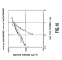
- the lattice mismatch is 14%, and in a case of an InSb thin film with a thickness not more than 1 micrometer, high electron mobility cannot be obtained even if it is a single-crystal thin film. Further, with a reduction in film thickness to 0.5 micrometers, and even further, to 0.2 micrometers, the electron mobility of InSb rapidly lowers. This is shown by the experimental data indicated by the line of square marks in Fig. 10 .
- Fig. 10 is a graph showing a relationship (triangle marks) between the film thickness and electron mobility of the InSb thin film directly formed on a GaAs substrate.
- Patent Document 1 eliminates lattice mismatch by using a p-type or insulating InSb (doped) layer formed on an AlGaInSb layer as a buffer layer, and the film quality of InSb (undoped) as an operation layer formed on the buffer layer is secured.
- Non-Patent Document 1 in the InSb thin film directly formed on the GaAs substrate, the existence of a low-electron mobility layer formed in the vicinity of a hetero interface between the GaAs substrate and InSb due to lattice mismatch based on a 14% difference in the lattice constant between the GaAs substrate crystal and InSb, and the existence of a low-electron mobility layer naturally formed on the InSb thin film surface are described. Due to low-electron mobility layers on both surfaces of the InSb thin film, the electron mobility becomes smaller (lower) as the InSb film thickness becomes smaller. Particularly, when the InSb film becomes thinner than 0.2 micrometers, the electron mobility lowering of the InSb thin film is remarkable, and manufacturing of an InSb Hall element with practical sensitivity is conventionally difficult.
- This electron mobility lowering of the InSb thin film according to film thickness reduction corresponds to the existence of a low-electron mobility layer produced at the hetero interface with the GaAs substrate and the thickness thereof during crystal growth.
- the thickness of this low-electronmobility layer is generally 0.1 to 0.2 micrometers although this depends on the crystal growth conditions. To increase the electron mobility of the InSb thin film at very small thin film thickness, it is necessary to reduce or eliminate the thickness of the low-electron mobility layer.
- Non-Patent Document 1 it is known that the InSb thin film grown on the GaAs substrate greatly changes in electron mobility and electron concentration in the thickness direction, and describing based on a simple model of distribution of properties of the thin film, these changes consist of a low-electron mobility layer which is in contact with the hetero interface with the substrate and is grown first (layer which has many defects due to lattice mismatch with the substrate and is not excellent in physical properties), and a high-electron mobility layer (layer which is not influenced by mismatch and is improved in physical properties and have very few defects) .
- the high-electron mobility layer with high electron mobility is thick, that is, by reducing the thickness ratio of the low-electron mobility layer, the electron mobility of the InSb thin film increases, and a magnetic sensor such as a high-sensitivity Hall element can be manufactured.
- the high-electron mobility layer can be easily increased in thickness by simply increasing the InSb film thickness, however, in this case, an input resistance becomes smaller when a magnetic sensor is manufactured, and this poses a problem such as an increase in power consumption of the magnetic sensors, and is disadvantageous in practicability.
- the InSb thin film mustbethinned, however, in this case, the high-electronmobility layer becomes extremely thin or, depending on circumstances, it completely disappears, so that an InSb thin film with high electron mobility cannot be obtained.
- the high-electronmobility layer becomes extremely thin or, depending on circumstances, it completely disappears, so that an InSb thin film with high electron mobility cannot be obtained.
- the low-electron mobility layer becomes thicker than the high-electron mobility layer, and as a result, the electron mobility is not as high as expected.
- the InSb film thickness is not more than a thickness substantially corresponding to the thickness of the low-electron mobility layer formed in the vicinity of the hetero interface or occupies 50% or more of the film thickness, the electron mobility extremely lowers, and therefore, it is conventionally impossible to manufacture a practical magnetic sensor such as a high-sensitivity Hall element.
- a practical magnetic sensor such as a high-sensitivity Hall element.
- the electron mobility which determines the sensitivity of the magnetic sensor becomes extremely low.
- the electron mobility of an InSb thin film with a thickness of 1.0 micrometer directly formed on a GaAs(100) substrate exceeds 50,000 cm 2 /Vs, however, the electron mobility of an InSb thin film with a thickness of 0.3 micrometers is about 20,000 cm 2 /Vs, and in the case of a film thickness of 0.2 micrometers, the electron mobility is not more than 10,000 cm 2 /vs, and in the case of an InSb thin film with a thickness of 0.15 micrometers, the electron mobility is about 7000 cm 2 /Vs or less, and in the case of 0.1 micrometers, the electron mobility is not more than 5, 000 cm 2 /Vs or less, so that the electron mobility rapidly lowers according to film thickness reduction. From this fact, it is understood that the thickness of the layer portion with low electron mobility of the InSb thin film is 0.
- the electron mobility rapidly lowers with an InSb film thickness reduction, and reaches an extremely small value. Therefore, the sensitivity of the magnetic sensor using this InSb thin film in the sensor section rapidly lowers with the InSb film thickness, and a magnetic sensor such as a high-sensitivity practical Hall element or magneto resistance element cannot be manufactured.
- the electron mobility greatly changes according to the film thickness of InSb due to a great lattice mismatch, that is, the electronmobility rapidly lowers with a filmthickness reduction.
- Non-Patent Document 1 a thin layer which has low electron mobility and an about 50 nanometer thickness was also found on the surface layer of the InSb thin film from a detailed examination of the phenomenon of electron transfer in the InSb thin film.
- the cause of this is considered that, when the substance is neither air in nor a vacuum, the lattice of the portion with a thickness of about 50 nanometers inside the InSb surface is strained and forms a thin layer with low electron mobility.
- This low-electron mobility layer on the surface portion also influences the film thickness dependency which lowers with the InSb film thickness reduction.
- an InSb thin film with high electron mobility cannot be manufactured.
- the thickness of this is about 0.2 micrometers.
- the comparatively thick low-electron mobility layers formed in the vicinities of the interface between the InSb thin film and the substrate and the surface of the InSb thin film caused by the above-described various factors are a big problem. That is, it is a big obstacle or problem to manufacture a practical magnetic sensor using an extremely thin film of InSb as a magnetic sensor section, and elimination or reduction in thickness of the low-electron mobility layers to be extremely thin are extremely important technical issues that should be solved.
- a magnetic sensor such as a Hall element
- high reliability has been conventionally demanded. That is, in industrial use or use as an in-vehicle sensor, provision of high performance in reliability relating to practical use such as improvement in reliability, durability, and environment resistance performance have been demanded. Therefore, it has been demanded that a protective film, that is, a passivation film for the InSb thin film surface is formed.
- a protective film that is, a passivation film for the InSb thin film surface is formed.
- the sensor section of the InSb thin film is made to approach a distance of several tens of micron, micron, and still further, submicron to a measuring target and detects the magnetic field. Therefore, it is required that a protective filmof the InSbthin-filmsurface is formed so as not to damage the InSb thin film or the surface thereof when measuring the magnetic field.
- an insulating film for example, an insulating film of Si 3 N 4 or SiO 2 , etc.
- a protective layer or a protective film is formed.
- This protective layer is different not only in the crystal lattice but also in the lattice constant from InSb, and further, in the case of manufacturing by plasma CVD, the surface of InSb is exposed to collision of plasma ions, and is frequently damaged.
- the protective layer may not be formed, however, in the manufacturing process of the magnetic sensor, this protective layer is ordinarily formed and is essential.
- the sensitivity lowers by about 10% (electron mobility lowering of the InSb thin film) according to the insulating film formation when an InSb thin film with a thickness of 1 micrometer is manufactured as a Hall element, however, if the thickness is reduced, this lowering remarkably increases, and in the case of a thickness of 0.3 microns, this sensitivity lowering amount is 40% to 70% and more depending on circumstances.
- Table 1 shown below shows the relationship between the lowering in electron mobility of the InSb thin film and the InSb film thickness when SiN with a thickness of 0.3 micrometers is formed on the surface.
- the surface of the InSb thin film is broken due to an impact of the plasma CVD or lattice mismatch, and the electron mobility of the broken portion becomes lower, and a comparatively thick layer with low electron mobility is formed in the vicinity of the surface in the InSb thin film, and as a result, great performance deterioration in the InSb thin film is caused.
- This low-electron mobility layer has a thickness of 50 to 100 nanometers (0.10 to 0.05 micrometers) although this depends on the conditions of protective layer formation, and is thicker than the thickness of 50 nanometers of the low-electron mobility layer which is naturally formed on the surface of the InSb thin film.
- the InSb thin film formed by epitaxial growth on the substrate it is essential to make the InSb thin film as thin and small as possible or eliminate the low-electron mobility layer formed in contact with a hetero interface between the InSb thin film surface and the substrate.
- a solution for such problems of performance deterioration in the InSb layer relating to the protective film formation has been demanded for a long time. That is, an InSb magnetic sensor structure which does not cause performance fluctuation in the process of manufacturing the InSb thin film as an element by avoiding deterioration in performance of the InSb thin film due to formation of insulation, that is, a protective layer on the surface of the magnetic sensor section or realization of an element structure which does not structurally cause performance deterioration in the InSb thin film has been demanded.
- the present invention was made in view of these problems, and an object thereof is to provide a thin film lamination to be used for a micro InSb thin film magnetic sensor which can directly detect magnetic flux density with high sensitivity and whose power consumption are small, an InSb thin film magnetic sensor using the same thin film lamination, and a method for manufacturing the same.
- the present invention was made to achieve the above-described object, and the present invention provides a thin film lamination that includes an InSb layer as an InSb thin film formed on a substrate and an Al x Ga y In 1-x-y Sb (0 ⁇ x, y ⁇ 1) mixed crystal layer which shows the property of resistance higher than that of the InSb layer or insulation and has a band gap larger than that of InSb, wherein the mixed crystal layer is provided between the substrate and the InSb layer, the content of Al and Ga atoms (x+y) is in the range of 5.0 to 17% (0.05 ⁇ x+y ⁇ 0.17) and lattice mismatch with the mixed crystal layer in contact with the InSb layer is in the range of 0.25 to 1.0%.
- the full width at half maximum of a rocking curve of the mixed crystal layer by X-ray diffraction from a (004) lattice plane is not less than 1 second and not more than 1300 seconds.
- the electron concentration of the InSb layer at room temperature is in the range of 1.2 ⁇ 10 16 to 5.0 ⁇ 10 18 cm -3 .
- the InSb layer is doped with any of donor impurities Sn, Si, S, Te, and Se.
- a second Al x GayIn 1-x-y Sb mixed crystal layer that is the same as the above-describedAl x Ga y In 1-x-y Sb mixed crystal layer is provided as an insulative semiconductor protective layer on the surface of the InSb layer opposite to the surface in contact with the substrate.
- the InSb layer has a low-electron mobility layer, and the low-electron mobility layer is in contact with the Al x Ga y In 1-x-y Sb mixed crystal layer, and has a thickness not less than 0.5 nanometers and not more than 30 nanometers.
- the low-electron mobility layer is in contact with the interfaces between the InSb layer (or operation layer) and the substrate, and the second Al x Ga y In 1-x-y Sb mixed crystal layer.
- the Al x GayIn 1-x-y Sb mixed crystal layer or the second Al x GayIn 1-x-y Sb mixed crystal layer is an Al x In 1-x Sb mixed crystal layer.
- the present invention provides a method for manufacturing a thin film lamination, includes at least the step of laminating the predetermined Al x Ga y In 1-x-y Sbmixed crystal layer on the substrate, then forming a low-electron mobility layer of InSb at a substrate temperature set so that its difference from the substrate temperature is within ⁇ 5 °C, and subsequently forming a high-electron mobility layer.
- the present invention provides an InSb thin film magnetic sensor using the InSb layer of the thin film lamination as a magnetic sensor section.
- the InSb layer is an operation layer of any of a Hall element, an element using the Hall effect, an element using the Hall effect, a magneto resistance element, and an element using the magneto resistance effect.
- the thickness of the InSb layer is not less than 8 nanometers and not more than 2,000 nanometers.
- the thickness of the Al x GayIn 1-x-y Sb mixed crystal layer is not less than 50 nanometers and not more than 3000 nanometers.
- the InSb layer is a single crystal.
- the thickness of the InSb layer is not less than 8 nanometers and not more than 300 nanometers.
- a second Al x GayIn 1-x-y Sb mixed crystal layer is provided as a semiconductor protective layer on the InSb layer.
- Al x GayIn 1-x-y Sb mixed crystal layer or second Al x Ga y In 1-x-y Sb mixed crystal layer, or both of these are Al x In 1-x Sb mixed crystal layers which do not contain Ga.
- the Al x GayIn 1-x-y Sb mixed crystal layer or second Al x GayIn 1-x-y Sb mixed crystal layer, or both of these are Al 0. In 0.9 Sb mixed crystal layers.
- GaAs layer is further provided on the second Al x Ga y In 1-x-y Sb mixed crystal layer.
- the InSb layer is doped with a donor impurity.
- the donor impurity belongs to group 4 or group 6 like Sn, Si, S, Te, or Se, etc.
- the InSb layer is doped with a donor impurity at a portion except 1.5 to 20 nanometers from the interface with the Al x GayIn 1-x-y Sb mixed crystal layer.
- a metal thin film as an electrode is formed in contact with a predetermined surface portion of the InSb tin film, and on at least the surface of the InSb thin film at the portion where the metal thin film is formed, and the donor impurity is doped with a large amount of a donor impurity than at other portions.
- the InSb thin film magnetic sensor is a Hall element or magneto resistance element.
- the present invention provides a method for manufacturing an InSb thin film magnetic sensor, including the step of laminating the Al x GayIn 1-x-y Sb mixed crystal layer at a predetermined substrate temperature on the substrate, then forming a low-electron mobility layer of the InSb thin film at a substrate temperature whose difference from the above-described substrate temperature is set within ⁇ 5 °C, and further forming a high-electron mobility layer.
- the inventors examined a technique for forming a new insulative or high-resistance layer between the thin film and the substrate for the purpose of solving electron mobility lowering relating to such film thickness dependency.
- a group III-V semiconductor which lattice-matches with InSb is only InSb, and InSb is still an n-type conductor at room temperature or a higher temperature even if it is doped with an impurity, so that InSb cannot be used as an insulating layer below the operation layer.
- the semiconductor including strain may cause strain relaxation from a high-temperature thermal effect or an impact from the outside, so that the inventors considered that use of this for a practical magnetic sensor usable even at a high temperature should be avoided.
- the inventors examined the possibility of magnetic sensor manufacturing, completely different from the conventional concept, by growing a high-quality InSb thin film involving crystal growth and a thin-film structure without assuming lattice match, that is, while assuming lattice mismatch although lattice match was preferable. As a result, the inventors found that a high-quality InSb thin film could be grown without assuming lattice match.
- the inventors focused on an Al x GayIn 1-x-y Sb (0 ⁇ x ⁇ 1) mixed crystal layer which was a less-mismatch material having a lattice constant close to that of InSb although it was not equal to InSb and whose insulation or high-resistance could be expected across a wide temperature range.
- this mixed crystal layer composed of three kinds of atoms becomes a material with a narrow band gap close to that of InSb, not an insulating layer.
- the crystal in this composition shows high-resistance, insulation, or p-type conductivity, and may function as an insulating layer on the substrate, and the examiners examined this.
- this Al x In 1-x Sb (0 ⁇ x ⁇ 1) mixed crystal layer for example, crystal can be grown on, for example, a GaAs substrate by selecting appropriate growth conditions according to molecular beam epitaxy.
- the Al proportion is small, it becomes conductive and does not function as an insulating layer.
- the lattice match to InSb is remarkably lost, so that lattice mismatch is great. Therefore, manufacturing of this Al x In 1-x Sb mixed crystal layer was not researched in detail in the past, and this material was impossible as an insulating layer for growing InSb thereon. Focusing on this material, the inventors repeatedly conducted experiments of growing an insulating layer by means of molecular beam epitaxy and growing an InSb thin layer on this insulating layer.
- this Al x In 1-x Sb (0 ⁇ x ⁇ 1) mixed crystal layer served as an insulative or high-resistance layer when appropriate proportions of Al and In were selected, and further, when the Al x In 1-x Sb (0 ⁇ x ⁇ 1) mixed crystal layer satisfied predetermined conditions, even if it does not have the same crystal lattice interval (lattice constant) as that of InSb, that is, it had lattice mismatch, if a certain condition is satisfied, an InSb thin film grown by means of molecular beam epitaxy on this mixed crystal layer had extremely high electron mobility although it was thin in thickness. That is, the thickness of the low-electron mobility layer with low electron mobility is reduced.
- an Al x Ga y In 1-x-y Sb (0 ⁇ x ⁇ 1, 0 ⁇ y ⁇ 1) mixed crystal layer composed of four kinds of atoms obtained by adding a slight amount of Ga to the Al x In 1-x Sb (0 ⁇ x ⁇ 1) mixed crystal layer composed of three kinds of atoms also served as an insulative or high-resistance layer by selecting appropriate composition parameters x and y, and further, when a certain condition was satisfied, an InSb thin film grown by means of molecular beam epitaxy on this layer had extremely high electron mobility.
- Al x GayIn 1-x-y Sb (0 ⁇ x ⁇ 1, 0 ⁇ y ⁇ 1) may be abbreviated to AlGaInSb, and similarly, Al x In 1-x Sb (0 ⁇ x ⁇ 1) may be abbreviated to AlInSb as appropriate.
- the resistivity of the mixed crystal layer rapidly decreases and becomes a conductive layer, and the Al x In 1-x Sb (0 ⁇ x ⁇ 1) layer does not play the role of the insulating layer.
- the electron mobility becomes 27, 000 cm 2 /Vs or more or, depending on the crystal growth conditions, 40,000 cm 2 /Vs or more even if the thickness is 0.15 micrometers.
- crystallinity of the Al x GayIn 1-x-y Sb (0 ⁇ x ⁇ 1) mixed crystal layer grown on the GaAs substrate and further, crystallinity of theAl x Ga y In 1-x-y Sb (0 ⁇ x ⁇ 1, 0 ⁇ y ⁇ 1) mixed crystal layer were investigated by using K ⁇ beam of Cu as an X-ray source and by investigating the relationship between the full width at half maximum of the rocking curve at a peak corresponding to the mixed crystal layer obtained from a (004) diffracted surface of the Al x GayIn 1-x-y Sb mixed crystal layer, in the X-ray diffraction conducted by using parallel beam optics of X-ray and InSb electron properties or a thickness of a low-electron mobility layer formed in the vicinity of the hetero interface.
- a layer with low electron mobility layer with a large electron concentration derived from a lattice defect of the portion with low electron mobility with more implantation caused by lattice mismatch
- the thickness of a layer with low electron mobility of 10,000 cm 2 /Vs or less is about 0.2 micrometers or 200 nanometers. Therefore, in an example in which an InSb layer that is thin, for example, has a thickness of 0.15 micrometers that is directly formed on a GaAs substrate, only low electron mobility as low as 7,000 cm 2 /Vs is obtained.
- a low-electron mobility layer formed within the InSb thin film at the hetero interface between the AlInSb mixed crystal layer as a ternary mixed crystal and InSb was extremely thin, and from thickness dependency of electron concentration, etc., the thickness was about 10 nanometers or at most 30 nanometers, so that it was found that this layer could be made extremely thin. Depending on circumstances, it was found that the low-electron mobility layer was about 3 nanometers in thickness.
- the present invention there is an extremely large difference in electron mobility of the InSb layer between the case where an extremely thin InSb conductive layer is formed on an Al x GayIn 1-x-y Sb (0 ⁇ x ⁇ 1, 0 ⁇ y ⁇ 1) mixed crystal layer satisfying the conditions of the above-described lattice mismatch and the full width at half maximum of 1300 seconds of X-ray diffraction of the above-described mixed crystal layer and the case where the InSb layer is directly formed on the GaAs (100) substrate without forming the mixed crystal layer.
- the AlInSb mixed crystal layer satisfying the conditions for obtaining high electron mobility of InSb. It is a matter of course that the crystal growth conditions when using MBE determine the crystallinity of the mixed crystal layer.
- the AlInSb mixed crystal layer must be insulative, and has a lattice constant close to that of InSb, so that its lattice mismatch with the substrate exists, and is not zero.
- the full width at half maximum of the X-ray diffraction peak is out of the range between 1 second and 1300 seconds, and further, if the crystal growth conditions are not appropriate, the full width at half maximum of the X-ray diffraction peak is not 1300 seconds or less.
- this minimum thickness also depends on the growth conditions of mixed crystals and the situation of the surface of the substrate, so that it is not obvious, however, in the case where appropriate crystal growth conditions are selected and maintained constantly, the quality of the mixed crystal layer is improved according to a thickness increase, so that it is preferable in normal cases that the thickness of the mixed crystal layer is at least 50 nanometers or more except in a special case, and when it is 600 nanometers or more, a mixed crystal layer whose full width at half maximum of the X-ray diffraction peak is 1300 seconds or less is stably obtained.
- the thickness of the low-electron mobility layer is 30 nanometers at maximum, 20 nanometers or less normally, and 10 nanometers or less when more preferable conditions are set.
- the minimum thickness is 1.5 nanometers. In other words, the thickness of the low-electron mobility layer is extremely thin.
- the low-electron mobility layer becomes extremely thin, and as a result, high electron mobility of the InSb conductive layer formed on AlInSb is obtained.
- the high-electron mobility layer with excellent crystallinity dominates electric conduction.
- the growth conditions for forming such a thin low-electron mobility layer are that the substrate temperature changes when the process shifts to the next InSb layer growing after finishing growing of the AlGaInSb layer is small.
- the substrate temperature changes when growing the AlGaInSb layer on InSb must also be small.
- the permissible difference in substrate temperature between the time of finishing theAlInSb growth and the time of starting the crystal growth of InSb is preferably 0 °C and ⁇ 5 °C at most when the optimal substrate temperature of InSb is set.
- an optimal value ⁇ 5 °C from the optimal temperature of InSb crystal growth is selected and determined.
- a substrate temperature when finishing the AlInSb growth a temperature ⁇ 5 °C from the optimal temperature of InSb crystal growth is determined.
- the substrate temperature when growing the second AlInSb layer on InSb layer and setting conditions for this are also the same.
- the inventors found 1) composition of the AlGaInSb layer (contents of A1 and Ga atoms in the range from 5.0 to 17%), 2) lattice constant difference, that is, lattice mismatch (lattice mismatch with the Al x Ga y In 1-x-y Sb mixed crystal layer in contact with InSb conductive layer in the range of 0.25 to 1.0%), and 3) full width at half maximum of 1300 seconds or less of the peak corresponding to the mixed crystal layer of a rocking curve of X-ray diffraction showing the quality of the crystallinity of the AlGaInSb mixed crystal layer.
- the difference in substrate temperature between the time of AlGaInSb growth and the time of InSb growth is within ⁇ 5 °C.
- the low-electron mobility layer formed inside the InSb thin film formed according to small lattice mismatch at the hetero interface between the InSb and the Al x Ga y In 1-x-y Sb mixed crystal layer could be set to be extremely thin in the range between 0.5 nanometers and 30 nanometers, 0.5 to 20 nanometers or less when more appropriate crystal growth conditions were selected (full width at half maximum is smaller, for example, 500 seconds or less) and the thickness was small, and 0.5 to 10 nanometers or less.
- an insulative or high-resistance Al x Ga y In 1-x-y Sb mixed crystal layer was grown on an InSb thin film.
- a substrate temperature at the time of crystal growth of the second AlInSb mixed crystals an optimal temperature within ⁇ 5 °C from the optimal temperature of InSb crystal growth is selected and determined.
- a substrate temperature at the time of starting AlInSb growth is most preferably the same as the optimal temperature of the InSb crystal growth, however, the temperature may be set to a temperature within ⁇ 5 °C from the optimal temperature.
- the InSb layer is extremely thin, if the surface is in contact with the air or it is used for manufacturing a magnetic sensor such as a Hall element or a magneto resistance element, remarkable deterioration in performance due to contact with inorganic films of SiO 2 or Si 3 N 4 to be used as a protective film, stress when resin-packaging, or influences from heterogeneous organic materials frequently occurs.
- the protective film was directly formed on InSb, 40 to 70% deterioration in performance was observed, however, when the Al x GayIn 1-x-y Sb mixed crystal layer was formed on the InSb thin film, performance deterioration in InSb due to formation of the mixed crystal film does not occur.
- the Al x GayIn 1-x-y Sbmixedcrystal layer has a great function like a semiconductor protective film for preventing deterioration in performance of the InSb layer, and further preventing performance deterioration in the InSb layer due to influences from the above-described protective film and package.
- Such an insulative thin layer or protective layer formed on the operation layer of the InSb thin film is also called a cap layer (or a semiconductor protective layer).
- the Al x GayIn 1-x-y Sb mixed crystal layer as such an insulative semiconductor protective layer has a band gap larger than that of InSb, so that it also serves as a potential barrier layer constituting a quantum well of InSb when the InSb layer is extremely thin, so that it may simply be called a potential barrier layer or a barrier layer.
- a GaAs layer is often further formed to make the protective layer firmer by the combination of these layers. This GaAs layer has oxidation resistance more excellent than that of AlGaInSb layer and is frequently used.
- the same substrate temperature at the time of AlGaInSb growth is preferable, however, it is not especially limited.
- the present inventors found that, although the above-described conditions about lattice matching must be satisfied, if the lattice mismatch with InSb was in the range of 0.25 to 1.0%, the Al x Ga y In 1-x-y Sb mixed crystal layer was extremely effective as a surface protective layer of the InSb thin film. In the case of this surface protective layer, it was also found that crystal of InSb was not grown thereon, so that the condition about the full width at half maximum of the X-ray did not influence greatly.
- the thickness of InSb is extremely small, so that the crystallinity comes into question as in the case of the buffer layer formed on the hetero interface, and the conditions about lattice matching and the conditions about the X-ray full width at half maximummust be satisfied to obtain high electron mobility of InSb.
- the degree of crystallinity depends on the film thickness of InSb, and more excellent crystallinity is required as the InSb thickness becomes smaller.
- the low-electron mobility layer formed in the vicinity of the surface of the InSb thin film in contact with the cap layer is thinner than in the case where no cap layer is formed, and is as thin as 30 nanometers or less, 20 nanometers or less, or 10 nanometers or less in thickness, and the minimum thickness is 0.5 nanometers.
- a thin layer of a group II I-V compound semiconductor which was insulative and has a lattice constant close to that of InSb was preferable and excellent as the semiconductor protective layer.
- the inventors completed a technique for obtaining electron mobility not less than 30, 000 cm 2 /Vs even when the thickness of InSb is as thin as 0.15 micrometers or less, and electron mobility of 20,000 cm 2 /Vs or more even when the thickness is 0.05 micrometers and completed a technique for manufacturing a high-sensitivity InSb thin-film magnetic sensor by applying said technique to the magnetic detecting section of a high-sensitivity practical magnetic sensor such as a Hall element or a magneto resistance element for the first time.
- a high-sensitivity practical magnetic sensor such as a Hall element or a magneto resistance element for the first time.
- the inventors manufactured a thin-film lamination in which the low-electron mobility layer at the hetero interface was extremely thin, or the low-electron mobility layer on the InSb surface was made extremely thin, and completed and realized a magnetic sensor such as an InSb Hall element or magneto resistance element in which both of the low-electron mobility layers were extremely thin and a technique for manufacturing this magnetic sensor.
- a magnetic sensor such as an InSb Hall element or magneto resistance element in which both of the low-electron mobility layers were extremely thin and a technique for manufacturing this magnetic sensor.
- the low-electron mobility layer can be made extremely thin in both cases where the InSb thin film of the magnetic sensor section is doped and not doped with donor atoms.
- the low-electron mobility layer can be made extremely thin. The same applies to the case of a magneto resistance element.
- the high-sensitivity InSb thin-filmmagnetic sensor having a magnetic sensor section of the thin-film lamination in which an InSb thin film that is epitaxially formed on a substrate and has electron concentration in the range of 1.2 ⁇ 10 6 to 5.
- the high-sensitivity InSb thin film magnetic sensor has a magnetic sensor section of a thin film lamination in which a sheet resistance of the Al x Ga y In 1-x-y Sb
- the high-sensitivity InSb thin filmmagnetic sensor has a magnetic sensor section consisting of an InSb thin film lamination in which a thickness of a low-electron mobility layer formed in the vicinity of a hetero interface between an InSb layer and an Al x Ga y In 1-x-y Sb mixed crystal layer is preferably 20 nanometers or less, and more preferably, 10 nanometers or less.
- the band gap difference at the hetero interface at which the Al x Ga y In 1-x-y Sb mixed crystal layer and the InSb are in contact with each other is not especially limited as long as the Al x GayIn 1-x-y Sb layer has insulation or high resistance, however, it is preferably 0.3 eV or more.
- a high-sensitivity InSb thin film magnetic sensor has a magnetic sensor section that is a Hall element, an element using the Hall effect, a magneto resistance element, or an element using the magneto resistance effect.
- the full width at half maximum of X-ray diffraction peak of the Al x GayIn 1-x-y Sb mixed crystal layer is preferably 1000 seconds or less, more preferably 500 seconds or less.
- the thickness of the InSb thin film of the magnetic sensor section is not especially limited, however, preferably 8 nanometers or more and 2, 000 nanometers or less, more preferably 1,000 nanometers or less, still more preferably 500 nanometers or less, and the most preferable range is 300 nanometers or less.
- the thickness is 200 nanometers or less, the effect of the present invention is great, and even when the thickness is 100 nanometers or less, the electron mobility of InSb is extremely high, so that a magnetic sensor with high sensitivity for magnetic fields and high input resistance can be manufactured.
- the permissible thickness of the low-electron mobility layer to be formed in contact with the hetero interface of the InSb thin film layer of the operation layer with the Al x GayIn 1-x-y Sb mixed crystal layer changes depending on the thickness of the InSb layer.
- the thickness of the operation layer is 150 nanometers or more, 30 nanometers is permissible, however, a smaller thickness is preferable.
- the thickness of the low-electron mobility layer is preferably 20 nanometers or less, and in the case of an operation layer with a thickness of 50 nanometers or less, the thickness of the low-electron mobility layer must be 5 nanometers or less.
- the full width at half maximum of the X-ray diffraction peak of the mixed crystal layer is preferably small, however, when the thickness of the InSb thin film of the operation layer is thin, a smaller full width at half maximum is preferable, and in the case of a thickness of 200 nanometers or less of InSb, 1300 seconds or less is permissible, however, 1000 seconds or less is preferable, and more preferably, 500 seconds or less. These conditions are obtained when the thickness of the AlGaInSb layer is set to 0.7 to 1.0 micrometers.
- the InSb layer formed on the Al x Ga y In 1-x-y Sb mixed crystal layer as an insulating layer formed on the substrate is shown by way of example, however, in some cases, on the upper surface (on the opposite side of the substrate) of the InSb layer, an Al x GayIn 1-x-y Sb mixed crystal layer (0 ⁇ x, y ⁇ 1) is formed which is the same insulating layer as described above, and has a content of Al and Ga atoms (x+y) in the range of 5.0 to 17% (0.05 ⁇ +y ⁇ 0.17), or lattice mismatch with the insulative Al x Ga y In 1-x-y Sb mixed crystal layer in contact with the InSb conductive layer is in the range of 0.25 to 1.0%.
- the Al x Ga y In 1-x-y Sb mixed crystal layer as an insulating layer formed on the upper surface of the InSb thin film operation layer preferably has crystallinity with a full width at half maximum of 1300 seconds or less of a rocking curve of X-ray diffraction from the (004) lattice plane although this is not essential.
- the low-electron mobility layer formed on the surface of the InSb layer in contact with an air layer is thin and estimated to be 50 nanometers or less at a maximum, however, when an inorganic protective layer, for example, Si 3 N 4 or SiO 2 , etc., is formed on the surface of InSb for the purpose of provision of reliability and forming a protective layer when manufacturing a magnetic sensor, a thickness of a damaged layer of the InSb surface layer when the damage is caused when forming or lattice mismatch and in-plane strain after forming is more than 50 nanometers, and the performance such as electron mobility of the InSb thin film is frequently lost.
- an inorganic protective layer for example, Si 3 N 4 or SiO 2 , etc.
- the low-electron mobility layer of InSb formed according to this damage (in this case, can be referred to as a damaged layer) reaches a thickness of 50 to 100 nanometers according to great performance deterioration and film thickness dependency of the InSb thin film due to formation of the protective film, etc.
- Such performance change due to the protective film formation is generally grasped as fluctuation in the element manufacturing process, and must be reduced.
- the InSb layer is extremely thin, this process fluctuation is extremely great, so that it becomes impossible to manufacture a high-sensitivity magnetic sensor.
- an insulative semiconductor protective layer may be formed in contact with the upper surface of InSb.
- an insulative compound semiconductor thin layer is preferably used as a thin film to be formed in contact with the InSb layer.
- this semiconductor protective layer a material whose lattice mismatch with InSb is small is selected so as not to damage the surface of InSb. Therefore, this is also effective for reducing the thickness of the low-electronmobility layer formed in contact with the surface of InSb when appropriate conditions are selected.
- an Al x Ga y In 1-x-y Sb mixed crystal layer is formed on the upper surface (surface on the opposite side of the substrate) of the InSb thin film operation layer mainly for the purpose of protecting the surface portion of the InSb layer from strain from the protective layer and the package resin and damage in the element manufacturing process for forming these.
- the low-electron mobility layer on the InSb thin film surface can be set to a thickness equal to or less than that of a natural surface. In other words, the thickness of the low-electron mobility layer on the surface is minimized as in the case of the interface of InSb.
- the InSb thickness of the operation layer is not more than 0.5 micrometers, the effect of formation of the Al x GayIn 1-x-y Sb mixed crystal layer in contact with the upper surface of the InSb thin film is especially remarkable and preferable.
- the Al x GayIn 1-x-y Sb mixed crystal layer that functions as described above may be called a cap layer. Therefore, formation of the Al x GayIn 1-x-y Sb mixed crystal layer in contact with upper and lower surfaces of the InSb thin film of the magnetic sensor section is most preferable for manufacturing a magnetic sensor such as an InSb thin film Hall element sliding the thin film lamination of InSb of the present invention as a magnetic sensitive portion.
- a GaAs layer is further formed on the AlGaInSb protective layer to form a firmer protective layer by the combination of these layers. This GaAs layer has more excellent oxidization resistance than the AlGaInSb layer and is frequently used.
- the thickness of the InSb layer is 8 nanometers or more and 200 nanometers or less, that is, not more than 200 nanometers, it is necessary that the Al x GayIn 1-x-y Sb mixed crystal layer is formed on both surfaces of the InSb thin film, the low-electron mobility layer is reduced, and process fluctuation cousing the performance reduction of the InBs is reduced or prevented, and these are preferably realized according to the present invention.
- the present invention for manufacturing a magnetic sensor including an operation layer with a thickness of 100 nanometers or less, more specifically, an InSb layer with a thickness of 60 nanometers or less is used for the purpose of manufacturing a quantum well structure, that is, confining electrons as carriers in the InSb layer.
- an Al x GayIn 1-x-y Sb mixed crystal layer may be formed on the upper surface (surface on the opposite side of the substrate) of the InSb thin film operation layer, and even in this case, reduction, etc., of the low-electron mobility layer in the above-described Al x Ga y In 1-x-y Sb mixed crystal layer and the InSb layer is equally realized in the vicinity upper and lower surfaces.
- the thickness of the low-electron mobility layer is at the same level on the upper and lower surfaces.
- the InSb thin film of the magnetic sensor section is manufactured by means of molecular beam epitaxy, however, the method is not limited and MOCVD or other methods may be used as long as the desired controlled properties such as electron mobility and sheet resistance are obtained. Further, in the present invention, the InSb thin film operation layer may be single crystal or polycrystal, however, single crystal is more preferable.
- a thin film lamination includes an InSb layer as an InSb thin film formed on a substrate; and an Al x Ga y In 1-x-y Sb mixed crystal layer (0 ⁇ x ⁇ 1, 0 ⁇ y ⁇ 1) which shows resistance higher than in the InSb layer, insulation, or p-type conductivity, and has a band gap larger than in InSb, the mixed crystal layer is provided between the substrate and the InSb layer and has a content of Al and Ga atoms (x+y) in the range of 5.0 to 17% (0.05 ⁇ x+y ⁇ 0.17) or lattice mismatch in the range of 0.25 to 1.0% with a mixed crystal layer in contact with the InSb conductive layer, so that a thin film lamination to be used for a micro InSb thin film magnetic sensor which can directly detect a magnetic flux density with high sensitivity and has small power voltage and consumption current, and a high-sensitivity InSb thin film magnetic sensor using the same thin film lamination, can be realized.
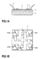
- Fig. 1A is a cross sectional construction view showing an embodiment of an InSb thin film magnetic sensor using a thin film lamination of the present invention as a magnetic sensor section;
- Fig. 1A and Fig. 1B are drawings showing an embodiment of an InSb thin film magnetic sensor using, as a magnetic sensor section, a thin film lamination including an InSb thin film as an operation layer of the present invention, and are construction views of a Hall element as an InSb thin film magnetic sensor using an InSb thin film as a magnetic sensor section or a magnetic detecting section, Fig. 1A is a sectional structural view and Fig. 1B is a structural view from the upper surface.
- the reference numeral 1 denotes a substrate
- 2 denotes an Al x Ga y In 1-x-y Sb mixed crystal layer (insulating layer)
- 3 denotes an operation layer and is an InSb thin film which causes a Hall effect in response to application of a magnetic field
- 4 (41, 42, 43, 44) denotes four terminal electrodes for external connection
- 5 denotes an electrode connection portion
- 6 denotes a wire connected to a lead.
- the magnetic sensor section of the central portion shows the sectional structure of the thin film lamination of the present invention.
- an Al x GayIn 1-x-y Sb mixed crystal layer (insulating layer) 2 is provided on the substrate 1, and on this layer, an InSb thin film which causes a Hall effect in response to application of a magnetic field, that is, operation layer 3 is further provided, and on the ends of this operation layer 3, terminal electrodes 4 are provided via electrode connection portions 5. Further, wires 6 are attached to the respective terminal electrodes 4.
- the thin film magnetic sensor comprises an InSb layer 3 as an InSb thin film formed on an Al x Ga y In 1-x-y Sb mixed crystal layer (0 ⁇ x, y ⁇ 1) 2 formed on the substrate 1, which shows resistance higher than that of the InSb layer 3, insulation, or p-type conductivity and has a band gap larger than that of InSb.
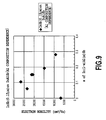
- This mixed crystal layer 2 is constructed so that, as shown in Fig. 9 , the content of Al and Ga atoms (x+y) is in the range of 5.0 to 17% (0.05 ⁇ x+y ⁇ 0.17) and the full width at half maximum of a rocking curve of X-ray diffraction from the (004) lattice plane is 1 second or more and 1300 seconds or less, and is present between the substrate 1 and the InSb layer 3.
- the content of Al and Ga atoms (x+y) is in the range of 5.0 to 17% (0.05 ⁇ x+y ⁇ 0.17) and the full width at half maximum of a rocking curve of X-ray diffraction from the (004) lattice plane is 1 second or more and 1300 seconds or less, and is present between the substrate 1 and the InSb layer 3.
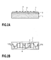
- Fig. 2A and Fig. 2B are drawings showing another embodiment of the InSb thin film magnetic sensor using, as a magnetic sensor section, a thin film lamination including the InSb thin film as an operation layer of the present invention, and are construction views of a magneto resistance element having two terminals and a plurality of short-bar electrodes.
- Fig. 2A is a sectional structural view
- Fig. 2B is a structural view from the upper surface.
- Components having the same function in Fig. 1A and Fig. 1B are attached with the same reference numerals.
- the reference numeral 3 denotes an operation layer which shows a resistance change in response to application of a magnetic field.
- the reference numerals 7 denote two terminal electrodes
- 8 denotes short-bar electrodes for increasing magneto resistance changes.
- the magneto resistance element section that is, the magnetic sensor section has two terminal electrodes 7 for external connection on both ends, and on the InSb thin film 3 provided between these terminal electrode 71 and terminal electrode 72, a plurality of short-bar electrodes 8 are arranged.
- the substrate 1 of the thin film lamination using an InSb thin film as an operation layer of the present invention normally, a substrate which is made of a substance stable at a high temperature and has insulation or high resistance and has a flat surface is used. Therefore, an insulative single-crystal substrate whose surface is a smooth crystal surface is preferably used. Particularly, an insulative substrate of GaAs or InP, etc., ispreferablyused. Alternatively, an insulative or high-resistance thin layer is formed on the surface so that the surface of the thin film formed to substantially have insulation or high-resistance is equivalent to the flat substrate.
- an insulative compound semiconductor layer of GaAs or the like By further forming an insulative compound semiconductor layer of GaAs or the like on the surface of an Si single-crystal substrate having a thin insulating layer formed on the surface, an insulative smooth surface having the same crystal structure as in InSb is obtained, so that this is preferably used as a substrate. Sapphire which has excellent insulation property is also used as a preferable substrate.
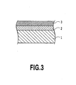
- Fig. 3 is a sectional construction view of a thin film lamination as a base of a magnetic sensor section consisting of an InSb thin film of the InSb thin film magnetic sensor of the present invention.
- an insulating layer 2 that is an Al x Ga y In 1-x-y Sb mixed crystal layer is provided, and thereon, an operation layer 3 of an InSb thin film which causes a Hall effect or resistance change in response to application of a magnetic field is further provided as a magnetic sensor section.
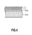
- Fig. 4 is a sectional construction view of another thin film lamination of the magnetic sensor section consisting of an InSb thin film of the InSb thin film magnetic sensor of the present invention, and an insulative or high-resistance thin layer made of an insulator such as SiO 2 or a semiconductor is formed on the surface of the substrate.
- the reference numeral 1 (11, 12) denotes a substrate, and on the surface of a first substrate 11, a substrate surface layer 12 that is an insulative or high-resistance thin film is provided.
- an Al x Ga y In 1-x-y Sb mixed crystal layer (insulating layer) 2 is provided, and thereon, an operation layer 3 is further provided.
- the substrate 1 used in the present invention must have heat resistance and insulation. Further, the insulation is not always necessary as long as an insulative or high-resistance Al x GayIn 1-x-y Sb mixed crystal layer 2 can be grown thereon. As shown in Fig. 4 , the substrate 11 is preferably insulative, however, the substrate 11 is allowed to have conductiveness as long as the insulative or high-resistance substrate surface layer 12 as shown in Fig. 4 can be formed.
- the surface of the substrate 1 must be flat.
- "Flat” mentioned herein means 0.2 nanometers or more and 10 nanometers or less of surface unevenness, preferably 5 nanometers or less, more preferably 1 nanometer or less, and in the most preferable case, lattice planes of crystals consisting of atoms forming the substrate are arranged with flatness corresponding to a one-atom layer on the surface of the substrate, that is, preferably, the substrate is a single-crystal substrate and has flatness corresponding to one-atom layer or less composed of lattice planes of crystals. Alternatively, flatness of one lattice plane interval or less is the most preferable flatness.
- the substrate 1 may be single crystal, polycrystal, or amorphous as long as it has insulation or high resistance, however, most preferably, it is single crystal with the same crystal structure as InSb, and further, single crystal of a group III-V compound semiconductor, and an insulating or semi-insulating substrate of GaAs, InP, GaN, or the like is preferable.
- surfaces of these single crystal plates are formed along the crystal lattice planes, and further, the surface may be formed with an angle from the crystal plane so as to make crystals easily grow thereon.
- a surface inclined in a range of 0 to 10 degrees from the substrate surface (100), (111), or (110), etc. may be formed and this is preferable.
- the surface of the substrate 1 can be used even on the index surface described above. Recently, it may be used on a high-index surface on which crystal growth has been attempted.
- the substrate 1 may be made of single-crystal Si, sapphire, high heat-resistance glass, or ceramic.
- the substrate 1 does not decompose at least when heated to 400 °C.
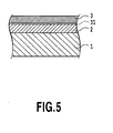
- Fig. 5 is a sectional construction view of details of another thin film lamination of the magnetic sensor section of the InSb thin film magnetic sensor of the present invention, showing a low-electron mobility layer formed inside the InSb thin film at the hetero interface between the InSb thin film and the Al x Ga y In 1-x-y Sb mixed crystal layer 2 and the substrate, and the reference numeral 31 clearly denotes a low-electron mobility layer.
- an insulating layer 2 is provided, and thereon, an operation layer 3 is provided, and inside this operation layer 3, generally, a low-electron mobility layer 31 is formed.
- an insulating layer made of a group III-V compound semiconductor like an AlGaInSb layer is preferably used.
- a thin layer of insulative or high-resistance GaAs or InP or a thin layer of GaN may be used.
- insulative or high-resistance ternary mixed crystals made of Al, Ga, and Sb insulative or high-resistance ternary mixed crystals made of Al, Ga, and Sb, quaternary mixed crystals made of Al, Ga, As, and Sb, quinary mixed crystals made of Al, In, Ga, As, and Sb, and multicomponent mixed crystals according to these elements may be used.
- a new element may further be added as appropriate to these multicomponent mixed crystals, and this is also included in the technical scope of the present invention.
- a quinary mixed crystal it may be expressed as AlInGaAsSb in this specification, and this means as described above.
- the insulating layer indicated by the reference numeral 12 may be formed in a plurality with an inclined composition which is changed in order (x, y, z, ⁇ , and ⁇ are changed).
- the insulating layer may be formed by continuously changing the composition of one layer.
- Such an insulating layer of a compound semiconductor or the uppermost surface of the high-resistance layer 12 is single crystal or polycrystal having a lattice constant close to that of InSb, or single crystal or polycrystal with the same crystal structure as that of InSb for growing the mixed crystal layer.
- a substrate made of a material different from group III-V compound semiconductor such as single-crystal sapphire, Si, glass, silica glass SiO 2 , or alumina Al 2 O 3
- group III-V compound semiconductor such as single-crystal sapphire, Si, glass, silica glass SiO 2 , or alumina Al 2 O 3
- an insulating layer made of a group III-V compound semiconductor or a high-resistance layer 12 must be formed on the surface thereof, and this formation is preferable.
- on the uppermost surface of this layer for growing an Al x Ga y In 1-x-y Sb single-crystal or polycrystal layer whose surface is smooth, single crystal or polycrystal having the same crystal structure as Al x Ga y In 1-x-y Sb is formed.
- Si single-crystal When Si single-crystal is used as the substrate, it is conductive, so that an insulating or high-resistance layer of a group III-V compound semiconductor such as insulative GaAs, AlGaAs, etc., is directly formed on the surface of Si, or more preferably, for the purpose of securing insulation from the substrate, at least one insulating layer of insulative oxide such as SiO 2 , Al 2 O 3 , or rare earth metal or insulative nitride such as Si 3 N 4 is formed in advance on the surface of Si, and then, on the uppermost surface of this layer, single crystal or polycrystal with the same crystal structure as that of AlInSb is formed for growing a single-crystal or polycrystal layer with a smooth surface such as AlInSb.
- a group III-V compound semiconductor such as insulative GaAs, AlGaAs, etc.
- an InSb thin film operation layer 3 in a super-high vacuum by means of MBE at a total gas pressure of 8x10 -9 Torr or less of elements which have no relation to crystal growth such as hydrogen, helium, CO 2 , various carbon hydrides, oxygen, nitrogen (excluded when forming nitride), etc.
- an InSb thin film which can be used for a high-sensitivitymagnetic sensor such as a Hall element or magneto resistance element having an InSb conductive layer with high electron mobility even if its thickness is very thin is manufactured.
- a high-sensitivity InSb thin film magnetic sensor including a magnetic sensor section using this InSb thin film as an operation layer is manufactured.
- the thickness of the low-electron mobility layer 31 formed in contact with the hetero interface between the InSb thin film 3 and the Al x Ga y In 1-x-y Sb layer 2 is as extremely thin as 20 nanometers or less.
- the thickness of the InSb thin film 3 is not especially limited.
- the preferable thickness is in the range of 8 to 2000 nanometers, more preferably 8 to 700 nanometers.
- Fig. 5 shows a part of a section of the magnetic sensor section of the InSb thin film magnetic sensor of the present invention.
- a low-electron mobility layer 31 formed at the hetero interface between the InSb thin film and the substrate is shown.
- the thickness of the layer indicated as a thin low-electron mobility layer 31 becomes extremely small according to formation of the Al x Ga y In 1-x-y Sb mixed crystal layer 2 satisfying the conditions of the present invention, and becomes, for example, 30 nanometers or less or 20 nanometers or less.
- the electron mobility was dramatically increased even if the InSb thin film was extremely thin.
- the thickness of the InSb layer is the same, when an Al x Ga y In 1-x-y Sb layer satisfying the conditions of the present invention is formed, the electron mobility increases several times in comparison with the case where this layer is not formed.
- this electron mobility difference is especially remarkable, and an InSb thin film which dynamically improved the electron mobility, had a high sheet resistance, and was usable in a high-sensitivity magnetic sensor was realized.
- a high-sensitivity InSb thin film magnetic sensor which could not been realized if the film thickness of InSb was 0.3 micrometers or less is realized by the present invention.
- the thickness of this low-electron mobility layer depends on the thickness of the InSb layer, however, generally, it is about 20% or more of the thickness of the InSb layer when the thickness of the InSb layer is 0.3 micrometers or less.
- a condition for thinning the low-electron mobility layer at the hetero interface formed due to lattice mismatch is found, and as a result, even if the InSb thin film operation layer is thin, high electron mobility is obtained.
- a technique for a high-sensitivity magnetic sensor material and a technique for an insulating layer which could increase the electron mobility of InSb of an operation layer were newly born, and a high-sensitivity InSb thin film magnetic sensor was realized. Further, this brought about great effects such as realization, provision, improvement in performance, and reduction in cost, etc., of the new function of an electronic device system to which the high-sensitivity InSb thin film magnetic sensor was applied.
- the InSb thin film magnetic sensor of the present invention is used with the structure shown in a section in Fig. 1A , Fig. 2A , or Fig. 3 .
- it may be required to have extremely high durability and reliability.
- Fig. 6 is a drawing showing still another embodiment of the InSb thin film magnetic sensor of the present invention in which a protective layer that is an insulating layer is formed on the surface of an InSb thin film.
- the reference numeral 9 denotes a protective layer.
- a protective layer 9 is provided so as to cover the portion above the operation layer 3 of the InSb thin film and the ends of the electrode connection portions 5. This protective layer is generally formed in the process of manufacturing a magnetic sensor.
- a protective layer 9 that is an inorganic or organic insulating layer different from the group III-V compound semiconductor is formed on the surface of the magnetic sensor section made of an InSb thin film in some cases.
- a preferable material example of the protective layer 9 that is an inorganic insulating layer is Si 3 N 4 , SiO 2 Al 2 O 3 , etc.
- An example of the protective layer 9 of a preferable organic insulating layer is a polyimide or polyimide-based organic insulating layer.
- This protective layer 9 may have a lamination structure made of a plurality of materials, and this lamination structure may be a plurality of inorganic or organic layers, or may be an inorganic and organic composite layer formed by laminating an inorganic layer and an organic layer in order.
- this protective layer 9 is important, if InSb is thin, provision of the protective layer 9 poses a problem although it does not pose a problem when the thickness of InSb is 1 micrometer or more.
- InSb when such an inorganic or organic insulating layer 9 is directly formed on the InSb thin film, it damages the surface of the InSb thin film 3, and causes great lowering in electron mobility.
- This lowering is 30 to 70% or more as shown in Table 1 although this depends on the thickness of InSb. Particularly, when the thickness of InSb is as extremely thin as 0. 7 micrometers or less, 0.
- the influence from this protective layer 9 is great, and due to the impact and strain when forming the surface of the InSb thin film 3, it strains or damages the InSb thin film, and causes great lowering in electron mobility. It depends on the thickness of InSb, however, the lowering is 30 to 70% or more. Further, when the InSb thickness is 0.3 micrometers or less, normally, the lowering is about 40%, however, depending on the conditions, it reaches 70% or more, and causes performance deterioration such as a great change in sheet resistance of InSb although this depends on the thickness.
- An InSb thin film magnetic sensor which uses the thin film lamination of the present invention structured as shown in Fig. 7A and Fig. 7B as the magnetic sensor section to solve the problem and prevent performance deterioration even in the case where the protective layer 9 is provided, is shown.
- An example of a Hall element is shown in a section.
- Fig. 7A and Fig. 7B show still another embodiment of the InSb thin film magnetic sensor of the present invention.
- Fig. 7A is a sectional structural view of a Hall element including an insulative semiconductor protective layer (may be called cap layer) 10 formed on the surface of an InSb thin film.
- This semiconductor protective layer 10 may be formed by a plurality of layers, however, for simplicity, it is shown as one layer.
- a typical preferable semiconductor protective layer is an Al x Ga y In 1-x-y Sb mixed crystal layer.
- Fig. 7B is a sectional structural view of a Hall element including the insulative semiconductor protective layer 10 and the protective layer 9 which are formed on the surface of an InSb thin film.
- an Al x Ga y In 1-x-y Sb layer 10 which has a band gap larger than that of InSb is often formed on the operation layer 3.
- a protective layer 9 as a normal protective layer is preferably formed on this insulative semiconductor protective layer 10 formed in advance.
- the high-sensitivity InSb thin film magnetic sensor of the present invention is preferably used by forming such a semiconductor protective layer 10 in contact with the InSb thin film, however, depending on circumstances, only the semiconductor protective layer 10 is formed without forming the protective layer 9.
- Fig. 8 is a sectional structural view of still another thin film lamination of the magnetic sensor section of the InSb thin film magnetic sensor of the present invention, showing a low-electron mobility layer formed in contact with the hetero interface between the surface of the InSb thin film in contact with the Al x Ga y In 1-x-y Sb semiconductor protective layer 10 and the Al x Ga y In 1-x-y Sb mixed crystal layer 2.
- An insulating layer 2 is provided on the substrate 1, and thereon, an operation layer 3 is provided. Inside this operation layer 3, a low-electron mobility layer 31 is formed on the insulating layer 2 side and a low-electron mobility layer 32 is formed on the opposite side. On these layers, an insulative semiconductor protective layer 10 is further provided.
- the thickness of the low-electron mobility layer 32 naturally formed on the InSb thin film surface becomes 10 nanometers or less according to formation of the insulative semiconductor protective layer 10 although this thickness is normally about 50 nanometers, and its influence is reduced, so that the electron mobility of the InSb thin film is improved. This effect is especially great when the film thickness of InSb is small.
- the InSb thin film conductive layer shows high electron mobility even with a film thickness of 0.1 micrometers or less.
- the InSb thin film magnetic sensor of the present invention by sandwiching the InSb thin film of the magnetic sensor section by the Al x Ga y In 1-x-y Sb insulating layer 2 whose lattice constant is close to that of InSb and the Al x Ga y In 1-x-y Sb semiconductor protective layer 10 or the semiconductor cap layer 10, extremely high electron mobility can be obtained even if the film thickness of the InSb is small. Particularly, reduction in thickness of the electron mobility layers on both surfaces of the InSb thin filmto 10 nanometers or less is very advantageous.
- the thickness of the semiconductor protective layer 10 is not especially limited, however, preferably, not less than a certain thickness, and can be determined as appropriate.
- the effect as a cap layer is obtained even with the thickness of about 5 nanometers, however, as a thickness enabling this protective layer to sufficiently perform its function, for example, the range of 10 nanometers to 200 nanometers is preferable. Of course, a larger thickness is also allowed. Alternatively, the thickness is allowed to be smaller.
- the effect of the semiconductor protective layer is preferably made more perfect.
- a preferable example is a high-insulation GaAs layer.
- Another semiconductor protective layer may be thus formed on the semiconductor protective layer 10 or the semiconductor protective layer 10 consists of two layers although this is not shown. This two-layer semiconductor protective layer structure is effective and frequently used.
- the Al x Ga y In 1-x-y Sb insulating layer 2 and the cap layer 10 as an Al x Ga y In 1-x-y Sb semiconductor protective layer may consist of a plurality of layers. In this case, a layer on the side in contact with InSb must have a lattice constant close to that of InSb and high insulation.
- the second semiconductor insulating layer which does not come into contact with InSb or a second semiconductor protective layer is allowed to have lattice mismatch with InSb.
- the InSb thin film magnetic sensor including, as a magnetic sensor section, a thin film lamination using the InSb thin film of the present invention as an operation layer, it is required that the insulating layer 2 made of Al x Ga y In 1-x-y Sb mixed crystals or a cap layer 10 that is a semiconductor protective layer made of Al x Ga y In 1-x-y Sb mixed crystals is formed in contact with the InSb thin film, and InSb thin film laminations having these basic structures are all included in the technical scope of the present invention.
- the film thickness of the InSb layer of the present invention is not especially limited. Therefore, the film thickness of 1 micrometer or more is allowed, and in particular, even when the thickness of InSb is as extremely small as 0.7 microns or less, 0.5 micrometers or less, or 0.3 micrometers or less, the high electron mobility is maintained, and a great sheet resistance is obtained.
- the InSb thin film when the InSb thin film is sandwiched by the Al x Ga y In 1-x-y Sb insulating layer 2 and the cap layer 10 that is an Al x Ga y In 1-x-y Sb semiconductor protective layer, a magnetic sensor section which shows high electron mobility even if the thickness of InSb is 0.1 micrometers or less is obtained, and this is in the technical scope of the present invention.
- the low-electron mobility layer formed at the hetero interface of the InSb thin film can be thinned.
- doping of the InSb thin film with a donor impurity for the purpose of reducing temperature changes in resistance and electron mobility is also performed.
- a donor impurity a group VI element is preferable, and a group IV element is also preferably used.
- S, Se, Te, Si, Ge, Sn, or the like is used.
- Si and Sn are preferably used as a donor impurity when manufacturing the InSb lamination of the present invention by means of molecular beam epitaxy.
- Sn is a preferable material since its vapor pressure is easily controlled at a comparatively low temperature.
- an area up to 10 nanometers from the hetero interface with Al x Ga y In 1-x-y Sb is not doped with an impurity, and the remaining area, that is, an area from 10 nanometers to the surface is doped with the impurity.
- a method can be selected among several methods in which a part of the InSb layer is doped, or the entirety is doped with an impurity.
- the electron mobility of the InSb thin film is 30, 000 cm 2 /Vs or more. According to an example described later, even if the thickness of the InSb layer is 0.15 micrometers, an electron mobility of 28,000 cm 2 /Vs is obtained.
- a magnetic sensor which includes a thin film of InSb and has high electron mobility and high sensitivity, and further, a Hall element and a magneto resistance element including a thin film of InSb and having high sheet resistance, high input resistance, and small power consumption can be manufactured.
- a Hall element and a magneto resistance element including a thin film of InSb and having high sheet resistance, high input resistance, and small power consumption.
- electron mobility being several times as high as that in the case where the Al x Ga y In 1-x-y Sb layer is not formed is obtained. This difference is great, and increases and becomes conspicuous as the film thickness of InSb becomes thinner.
- the InSb layer is as extremely thick as 0.5 micrometers or less, 0.3 micrometers or less, or 0.1 micrometers or less, the difference becomes remarkable, and therefore, the electron mobility which enables manufacturing of a high-sensitivity magnetic sensor was realized for the first time by forming the Al x Ga y In 1-x-y Sb layer of the present invention.
- the electron mobility is about 7, 000 cm 2 /Vs.
- an InSb thin film with a thickness of 0.15 micrometers is manufactured on a GaAs substrate, only low electron mobility is obtained as described above, however, by forming an InAlSb layer 2 as an example of the Al x Ga y In 1-x-y Sb layer shown in Fig. 1 of the present invention, an electron mobility of 28, 000 cm 2 /Vs or, depending on the crystal growth conditions, 40,000 cm 2 /Vs or more can be obtained in comparison with the case where the InAlSb layer is not formed.
- This value is 4 to 5 times as high as that in the case where the InSb layer is directly grown.
- an InSb layer with a thickness of 0.3 micrometers is grown, an InSb single-crystal thin film with electron mobility as high as 40, 000 cm 2 /Vs or, depending on the crystal growth conditions, 50,000 cm 2 /Vs or more can be manufactured.
- the effect of improving the electron mobility corresponding to the sensitivity for magnetic field detection of the magnetic sensor is extremely great.
- the Al x Ga y In 1-x-y Sb layer of the present invention was formed as a cap layer on the surface of the InSb layer, when the InSb layer was extremely thin and an inorganic protective layer of Si 3 N 4 or SiO 2 , etc., was formed, 50% or more process fluctuation (sensitivity lowering) was observed if no cap layer was provided, however, according to the present invention, the process fluctuation was reduced to 5% or less, further, to 3% or less. Thus, the process fluctuation becomes so small that it does not pose a problem in performance of the magnetic sensor.
- the electron mobility increases 1.5 times or more when the thickness of the InSb layer is 0.7 micrometers or less, 2 times or more in the case of a thickness of 0.5 micrometers or less, 3 times or more in the case of a thickness of 0.35 micrometers or less, 4 times or more in the case of a thickness of 0.25 micrometers or less, and six times or more in the case of a thickness of 0.10 micrometers or less, and thus, the effect of the InAlSb layer is remarkable.
- the effect of obtaining high electron mobility of the InSb layer does not substantially change even when the InSb layer is doped with a donor impurity such as Si, Sn, Te, S, or Se.
- a donor impurity such as Si, Sn, Te, S, or Se.
- the donor impurity mentioned herein any one is usable as long as it provides n-type conduction for InSb, and as a preferable example, it is a group VI or IV element such as Sn, Si, Ge, C, S, Se, or Te.
- an Al x Ga y In 1-x-y Sb mixed crystal layer 2 is grown on a substrate 1 by means of molecular beam epitaxy, and then, an InSb thin film is epitaxially grown on the mixed crystal layer.
- the manufactured InSb thin film is processed according to a wafer process unique to the magnetic sensor of the present invention including the steps of pattern etching of the InSb thin film based on photolithography using a photosensitive resist, exposing the surface of the InSb layer by opening a window in a necessary portion of the Al x Ga y In 1-x-y Sb mixed crystals of the cap layer, forming an electrode pattern by forming a metal thin film on a necessary portion of InSb or an electrode contact portion where a window is opened and the surface of InSb is exposed by means of vapor deposition, sputtering, wet plating, etc., forming an inorganic protective layer on portions except for external connection bonding electrodes so as to cover the magnetic sensitive portion surface of the element as appropriate, and further, forming a thin layer having rubber elasticity of Si resin or the like so as to cover the magnetic sensitive portion by means of photolithography as appropriate, and then, many micro high-sensitivity InSb thin filmmagnetic sensors such as Hall elements or magneto
- the wafer is cut into individual Hall element chips, etc., by a dicing saw. Further, the chip of this InSb thin film magnetic sensor is generally packaged through a standard transfer mold process, subjected to performance inspection, and then completed as a product.
- a molecular beam epitaxy apparatus to be used for manufacturing a thin film lamination of the present invention is formed of a cylindrical vacuum chamber for maintaining a vacuum and includes at least a mechanism which holds horizontally a GaAs substrate for growing crystals thereon and a mechanism which provides periodic movement such as rotation for irradiating equally and uniformly vapors of constituent elements of the thin film to be formed on the substrate surface from evaporation sources.
- the molecular beam epitaxy apparatus is a crystal growing apparatus which includes means for carrying the substrate in and out of a crystal growth chamber in a state where a vacuum in the crystal growth chamber is maintained.
- This apparatus includes a resistance heater as a heat radiation source which is in proximity to a substrate having a GaAs (100) surface on which an InSb thin film is grown at the subsequent step and electrically heated to a high temperature and set on the opposite side of the InSb thin film growing surface, and a temperature sensor which can measure the substrate temperature.
- a resistance heater as a heat radiation source which is in proximity to a substrate having a GaAs (100) surface on which an InSb thin film is grown at the subsequent step and electrically heated to a high temperature and set on the opposite side of the InSb thin film growing surface
- a temperature sensor which can measure the substrate temperature.
- the apparatus includes a plurality of evaporation sources which can irradiate the substrate surface with vapor beams of elements charged in the evaporation sources at a predetermined intensity for a predetermined time, that is, a plurality of evaporation sources (Knudsen cells, called K-cells) as means for generating vapors of constituent elements for forming a thin film by electrical heating, temperature measuring sensors set in the respective evaporation sources to control the intensities of the vapors, and power supply means which are set corresponding to the respective evaporation sources to maintain a state of generating vapors of elements charged in the evaporation sources corresponding to predetermined vapor intensities and maintain the evaporation sources at a predetermined evaporation source temperature, and in addition, a power supply means.
- a power supply means which can irradiate the substrate surface with vapor beams of elements charged in the evaporation sources at a predetermined intensity for a predetermined time
- the molecular beam epitaxy apparatus as a crystal growing apparatus including a crystal growth chamber that has means such as shutters or valves which can cut off vapors generated from the evaporation sources, and further has a vapor intensity measuring device capable of measuring intensities of the vapors, while an accumulated vapor pressure of remaining impurity gases such as H 2 , CO, CO 2 He, N 2 , O 2 , etc., (excluding vapors of elements forming the thin film, for example, A S4 , A S2 , Sb 2 , Sb 4 , etc.) was maintained at 1 ⁇ 10 -8 Torr or less when the substrate is heated and irradiating As vapor containing As 4 or As 2 onto the (100) surface of the insulative GaAs substrate with a thickness of 0.35 millimeters and a diameter of 2 inches, the substrate was heated to 630 °C, and then controlled within 420 ⁇ 2 °C.
- impurity gases such as H 2 , CO, CO 2 He, N 2
- In and Sb were simultaneously evaporated at the substrate temperature of 420 ⁇ 2 °C to form a single-crystal InSb thin film with a thickness of 0.7 micrometers on the Al 0.1 In 0 . 9 Sb layer formed on the GaAs (100) surface. Further, the AlInSb layer grown on the GaAs (100) surface under these trial manufacturing conditions was subjected to an experiment of X-ray diffraction, and the crystallinity of the Al 0.1 In 0 . 9 Sb mixed crystal layer was evaluated. As a result, the full width at half maximum (FWHM) at the peak of the Al 0 .1In 0 .
- FWHM full width at half maximum
- the electron mobility of the InSb thin film manufactured with this structure is 53, 000 cm 2 /Vs, and the sheet resistance is 101 ⁇ /squire, and these electron mobility and the sheet resistance are extremely high.
- a magnetic sensor such as a Hall element or magneto resistance element having high sensitivity and high input resistance (with high sensitivity of 200 ⁇ or more) can be manufactured.
- the input resistance was 200 ⁇
- the Hall voltage in response to application of 50mT magnetic flux density when driven with a constant voltage of 1V was 132 mV.
- the sensitivity in a magnetic field was as high as 132 mV/V.50mT.
- the InSb thin film of Example 1 may be used as it is for manufacturing a magnetic sensor, and further, for the purpose of manufacturing a magnetic sensor with improved environment-resistance performance, a protective layer of Si 3 N 4 or SiO 2 , etc., is frequently formed as an environment protective layer by means of plasma CVD on the InSb thin film layer of Example 1.
- a protective layer of Si 3 N 4 or SiO 2 , etc. is frequently formed as an environment protective layer by means of plasma CVD on the InSb thin film layer of Example 1.
- a protective layer of Si 3 N 4 or SiO 2 , etc. is frequently formed as an environment protective layer by means of plasma CVD on the InSb thin film layer of Example 1.
- Si 3 N 4 to 0.3 micrometers was directly formed on the surface of InSb, at least 35 to 40% lowering in electron mobility and sheet resistance occurs although this depends on the thickness, and the performance of high sensitivity of the magnetic sensor expected at the beginning is lost and a magnetic sensor with desired high sensitivity cannot be manufactured.
- a semiconductor protective layer which is a semiconductor insulating layer whose lattice constant is close to that of InSb may be formed on the InSbthin film.
- This semiconductor insulating layer may consist of one layer or two layers, however, as a surface in contact with the InSb thin film, an AlInSb or AlGaInSb layer whose lattice constant is close to that of InSb is formed.
- an InSb thin film with the same thickness of 0. 7 micrometers as in Example 1 was formed according to the same method.
- an Al 0.1 In 0 was formed on the InSbthin film.
- a GaAs layer was formed at a substrate temperature of 420 ⁇ 2 °C, and thereon, a GaAs layer was further formed to form a cap layer, that is, a semiconductor protective layer that was a semiconductor insulating layer.
- a single-crystal Al 0 .1In 0 . 9 Sb mixed crystal thin film (with a lattice constant difference of 0.5% from InSb) which hadatomicity proportions of 90% In and 10% Al and had insulation or semi-insulation or high resistance was grown to a thickness of 50 nanometers (0.05 micrometers).
- the electron mobility of the InSb thin film of this example was 51,600 cm 2 /Vs, and the sheet resistance was 97 ⁇ /square. There was no great performance change from Example 1, and high electron mobility and high sheet resistance were obtained.
- a high-sensitivity and high-input resistance (200 ⁇ or more) magnetic sensor such as a Hall element or magneto resistance element could be manufactured, so that it was proved that this InSb thin film lamination could be used for manufacturing a high-sensitivity magnetic sensor.
- this semiconductor protective layer By forming this semiconductor protective layer, an effect of reducing performance deterioration due to the above-described protective layer was obtained.
- 0. 3 micrometer Si 3 N 4 was formed on the GaAs layer that was the top layer by means of plasma CVD to form a protective layer, however, the lowering in electron mobility and sheet resistance was as small as 5% or less.
- great performance deterioration due to the protective layer did not occur, and performance of high electron mobility and high sheet resistance did not deteriorate even through the protective layer forming step.
- a magnetic sensor such as a Hall element or magneto resistance element having high sensitivity, high input resistance (with high sensitivity of 200 ⁇ or more), and extremely high environment resistance can be manufactured.
- the obtained performance of the element showed an input resistance of 205 ⁇ and a Hall voltage of 126 mV at 50 mT when driven with a constant voltage of 1V.
- the sensitivity in a magnetic field was as high as 126 mV/V.50mT.
- the performance of the Hall element is not greatly changed, so that most of the influence from the 0.3 micrometer Si 3 N 4 protective layer was eliminated by the formation of the AlInSb semiconductor insulating layer.
- an accumulated vapor pressure of remaining impurity gases for example, H 2 , CO, CO 2 He, N 2 , and O 2 , etc., (excluding vapors of elements forming the thin film, for example, As 4 , As 2 , Sb 2 , Sb 4 , etc.) was maintained at 1 ⁇ 10 -8 Torr or less when heating the substrate, an insulative GaAs substrate with a thickness of 0.35 millimeters and a diameter of 2 inches was heated to 630°C (controlled within ⁇ 2°C) while the (100) surface thereof was irradiated with As vapor containing As 4 or A s 2 (that is, a step for preventing separation of constituent elements forming the GaAs substrate surface), and then the temperature was lowered to 420 °C while irradiating As vapor, and next, according to a predetermined temperature pattern around 420°C,
- impurity gases for example, H 2 , CO, CO 2 He, N 2 , and O 2 , etc.
- vapors of elements charged in the evaporation sources that is, A1, In, and Sb were simultaneously made incident at a predetermined vapor pressure ratio (beam intensity ratio measured with a beam monitor) to grow 0.7 micrometers of a single-crystal Al 0.1 In 0.9 Sb mixed crystal thin film (with a lattice constant difference of 0.5% from InSb) which had atomicity proportions of 90% In and 10% Al and had insulation or semi-insulation or high resistance at a growth rate of 1 ⁇ m/h on the GaAs (100) surface.
- In and Sb were simultaneously evaporated from the evaporation sources charged with In and Sb, respectively, whereby a single-crystal InSb thin film with a thickness of 0. 3 micrometers and a sheet electron concentration of 5.8 ⁇ 10 11 /cm 2 was formed on the Al 0.1 In 0.9 Sb layer formed on the GaAs (100) surface.
- a single-crystal Al 0.1 In 0.9 Sb mixed crystal thin film (having a lattice constant difference of 0.5% from InSb) which had atomicity proportions of 90% In and 10% Al and had insulation or semi-insulation or high resistance was grown to a thickness of 50-nanometers (0.05 micrometers), and then 6-nanometer GaAs was grown.
- An InSb thin film of Example 3 manufactured with this structure has an electron mobility of 37,000 cm 2 /Vs and a sheet resistance of 300 ⁇ /squire, and these electron mobility and sheet resistance are extremely high, so that a magnetic sensor such as a Hall element or a magneto resistance element with high sensitivity and high input resistance (500 ⁇ or more) can be manufactured by using this InSb thin f ilm lamination as a magnetic sensitive portion.
- a magnetic sensor such as a Hall element or a magneto resistance element with high sensitivity and high input resistance (500 ⁇ or more) can be manufactured by using this InSb thin f ilm lamination as a magnetic sensitive portion.
- a Hall element with a high input resistance 200 ⁇ or more was manufactured.
- the performance of the element showed an input resistance of 550 ⁇ and a Hall voltage of 92 mV at 50 mT when driven with a constant voltage of 1V.
- the sensitivity in a magnetic field was as high as 92 mV/V.50mT.
- This element has an extremely high input resistance, so that its driving power is small.
- Si 3 N 4 is frequently formed to about 0.3 micrometers by plasma CVD on the surface of the uppermost GaAs (Al 0.1 In 0.9 Sb insulating layer when GaAs is not provided).
- the thickness of the InSb thin film is as thin as 1 micrometer or less as in the case of this example
- 0.3 micrometer Si 3 N 4 is directly formed on the InSb thin film with a thickness of 0.3 micrometers by means of plasma CVD
- insulative Al 0.1 In 0.9 Sb and GaAs (6 nanometers) as a semiconductor protective layer are formed on the InSb thin film, and even if 0.3 micrometer Si 3 N 4 is formed by plasma CVD, lowering in electron mobility and sheet resistance is as extremely small as 5%.
- a magnetic sensor such as a Hall element or magneto resistance element with high sensitivity, high input resistance (500 ⁇ or more) and high environment resistance reliability could be manufactured. Even if the step of forming the protective layer of Si 3 N 4 to 0. 3 micrometers by plasma CVD is added to the magnetic sensor manufacturing process, the performance of the manufactured element is not greatly changed.
- the obtained performance of the element showed an input resistance of 590 ⁇ and a Hall voltage of 89 mV at 50 mT when driven with a constant voltage of 1V. That is, the sensitivity in the magnetic field is as high as 89 mV/V.50mT, and the influence from sensitivity lowering caused by the protective layer is rarely observed.
- the formation of this 0.3 micrometer Si 3 N 4 protective film provided the Hall element with high reliability such as environment resistance performance and a lengthened lifetime.
- a molecular beam epitaxy apparatus as a crystal growing apparatus including a crystal growth chamber having the same function as in Example 1, an accumulated vapor pressure of remaining impurity gases, for example, H 2 , CO, CO 2 He, N 2 , and O 2 , etc., (excluding vapors of elements forming the thin film, for example, As 4 , As 2 , Sb 2 , Sb 4 , etc.) was maintained at 1 ⁇ 10 -8 Torr or less when heating the substrate, a GaAs substrate with a thickness of 0.35 millimeters and a diameter of 2 inches was heated to 620 °C while the (100) surface thereof was irradiated with As vapor containing As 4 or As 2 (that is, a step for preventing separation of constituent elements forming the GaAs substrate surface), and then the temperature was lowered and set to and maintained at 420 ⁇ 2 °C.
- impurity gases for example, H 2 , CO, CO 2 He, N 2 , and O 2 , etc.
- the input resistance was 164 ⁇ and a Hall voltage was 85 mV at 50 mT when driven with a constant voltage of 1V.
- the sensitivity in a magnetic field was as extremely high as 85 mV/V.50mT.
- Example 4 a single-crystal Al 0.1 In 0.9 Sb mixed crystal thin film (with a lattice constant difference of 0.5% from InSb) which had atomicity proportions of 90% In and 10% Al and had insulation or semi-insulation or high resistance was further grown to a thickness of 50 nanometers (0. 05 micrometers) on the InSb thin film, and then 6 nanometer GaAs was grown.
- the performance of InSb thin film showed an electron mobility of 34,000 cm 2 /Vs and a sheet resistance of 80 ⁇ /square although slight lowering in sheet resistance due to Sn doping and slight lowering in electron mobility due to impurity scattering were observed.
- the electron mobility and the sheet resistance were extremely high, and by using this InSb thin film as a magnetic sensitive portion, a magnetic sensor such as a Hall element or magneto resistance element with high sensitivity and high input resistance (180 ⁇ or more) can be manufactured, and as in the case of Example 4, this InSb thin film is usable for manufacturing a magnetic sensor with high sensitivity and less temperature dependency.
- temperature dependency (temperature coefficient) of the sheet electron concentration of the InSb thin film in the range of -40 to 150 °C around room temperature was reduced by one order, that is, reduced to 1/10 to 2/10 in comparison with Example 1.
- dependencies of the Hall voltage (magnetic field detection signal) when driven with a constant current and the input resistance of the Hall element of a Hall element manufactured by using the InSb thin film of this example as a magnetic sensor section were reduced by one order, that is, reduced to 1/10 to 2/10 in comparison with the undoped case.
- Performance of a Hall element manufactured without forming a 0. 3 micrometer insulating layer of Si 3 N 4 in the process of manufacturing the Hall element showed an input resistance of 175 ⁇ and a Hall voltage of 82 mV at 50 mT when driven with a constant voltage of 1V.
- the sensitivity in a magnetic field was as high as 82 mV/V.50mT.
- the input resistance is as sufficiently high as 175 ⁇ .
- the InSb thin film has a thickness of 0.3 micrometers and no semiconductor protective layer is provided, if Si 3 N 4 is directly formed on InSb, 35 to 50% or more lowering in electron mobility and sheet resistance occurs, and performance of the high sensitivity of the magnetic sensor expected at the beginning is lost.
- influence from the step of forming a protective layer of Si 3 N 4 to 0. 3 micrometers by plasma CVD on the element performance was investigated.
- the semiconductor protective layer is formed, so that the damage due to plasma CVD is as small as 3%, and basic performance of the Hall element such as the sensitivity of the Hall element, temperature dependency, and element resistance were not greatly lowered. Therefore, the performance of the manufactured Hall element was not changed from the element performance described above of this example in which Si 3 N 4 was not formed.
- an accumulated vapor pressure of remaining impurity gases for example, H 2 , CO, CO 2 He, N 2 , and O 2 , etc., (excluding vapors of elements forming the thin film, for example, As 4 , As 2 , Sb 2 , Sb 4 , etc.) was maintained at 1 ⁇ 10 -8 Torr or less when heating the substrate, an insulative GaAs substrate with a thickness of 0.35 millimeters and a diameter of 2 inches was heated to 630 °C (controlled within ⁇ 2°C) while the (100) surface thereof was irradiated with As vapor containing As 4 or As 2 (that is, a step for preventing separation of constituent elements forming the GaAs substrate surface), and then the temperature was lowered to 420°C while irradiating As vapor, and the substrate temperature was set to a predetermined 420 ⁇ 2 °
- Al, In, and Sb were simultaneously made incident with a predetermined vapor pressure ratio (beam intensity ratio measured with a beam monitor) to grow a single-crystal Al 0.1 In 0.9 Sb mixed crystal thin film (with a lattice constant difference of 0.5% from InSb) which had atomicity proportions of 90% In and 10% Al and had insulation or semi-insulation or high resistance to a thickness of 0.7 micrometers at a growth rate of 1 micrometer/h on the GaAs (100) surface.
- a predetermined vapor pressure ratio beam intensity ratio measured with a beam monitor
- In and Sb were simultaneously evaporated from the evaporation sources at the substrate temperature of 420 ⁇ 2 °C, and whereby a single-crystal InSb thin film with a thickness of 0.15 micrometers was formed on the Al 0.1 In 0.9 Sb layer. Further, on the InSb thin film, a single-crystal Al 0.1 In 0 . 9 Sb mixed crystal thin film (with a lattice constant difference of 0. 5% from InSb) as a semiconductor protective layer which had atomicity proportions of 90% In and 10% Al and had insulation or semi-insulation or high resistance was grown to a thickness of 50 nanometers (0.05 micrometers), and then 6 nanometer GaAs was grown. The substrate temperature was constantly kept at 420°C over the entire period of this mixed crystal thin film formation.
- the electron mobility of the manufactured InSb thin film was 28,000 cm 2 /Vs, the sheet resistance was 700 ⁇ /square, and the sheet electron concentration was 3.3 ⁇ 10 11 /cm 2 .
- These electron mobility and sheet resistance are extremely high, and by using this InSb thin film as the magnetic sensitive portion, a magnetic sensor such as a Hall element or magneto resistance element with high sensitivity and high input resistance (1,000 ⁇ or more) can be manufactured, so that it is obvious that this thin film can be used for manufacturing a high-sensitivity magnetic sensor whose power consumption is extremely small.
- the InSb thin film is as extremely thin as 0.15 micrometers as in the case of this example, if Si 3 N 4 is directly formed to 0.3 micrometers on the surface of InSb by means of plasma CVD, 60 to 70% lowering in electron mobility and sheet resistance occurs, and performance of high sensitivity of the magnetic sensor expected at the beginning is lost, so that a Hall element with desired performance cannot be manufactured.
- the performance showed a Hall voltage of 70 mV in a magnetic field of 50 mT when driven with 1V, and an input resistance of 1200 ⁇ .
- the sensitivity in the magnetic field was as high as 70 mV/V50mT. Further, high resistance showing an input resistance of 1200 ⁇ was obtained, so that a Hall element with extremely small power consumption when driven could be manufactured.
- an accumulated vapor pressure of remaining impurity gases for example, H 2 , CO, CO 2 , He, N 2 , and O 2 , etc., (excluding vapors of elements forming the thin film, for example, As 4 , As 2 , Sb 2 , Sb 4 , etc.) was maintained at 1 ⁇ 10 -8 Torr or less when heating the substrate, an insulative GaAs substrate with a thickness of 0.35 millimeters and a diameter of 2 inches was heated to 620 °C while the (100) surface thereof was irradiated with As vapor containing As 4 or As 2 , and then the temperature was lowered to 420 °C and kept at 920 ⁇ 2 °C that was an optimal substrate temperature when growing InSb crystals.
- impurity gases for example, H 2 , CO, CO 2 , He, N 2 , and O 2 , etc.
- Al, In, and Sb were simultaneously made incident at a predetermined vapor pressure ratio (beam intensity ratio measured with a beam monitor) to grow a single-crystal Al 0.1 In 0.9 Sb mixed crystal thin film (with a lattice constant difference of 0.5% from InSb) which had atomicity proportions of 90% In and 10% Al and had insulation or semi-insulation or high resistance to a thickness of 0.7 micrometers on the InP (100) surface at a growth rate of 1 micrometer/h.
- a predetermined vapor pressure ratio beam intensity ratio measured with a beam monitor
- the substrate temperature was kept at 420 ⁇ 2 °C, In and Sb were simultaneously evaporated from the evaporation sources, and further, Sn was evaporated from the evaporation source in which Sn is a donor impurity, whereby a single-crystal InSb thin film which had a thickness of 0.3 micrometers and was doped with Sn, and had a sheet electron concentration of 2.42 ⁇ 10 12 /cm 2 was manufactured on the Al 0.1 In 0.9 Sb layer formed on the InP (100) surface. Further, on this InSb thin film, a single-crystal Al 0.1 In 0.9 Sb mixed crystal thin film (with a lattice constant difference of 0.
- the performance of the InSb thin film showed an electron mobility of 38,200 cm 2 /Vs and a sheet resistance of 70 ⁇ /square although slight lowering in sheet resistance due to Sn doping and slight lowering in electron mobility due to impurity scattering were observed. These electron mobility and sheet resistance are extremely high, so that a magnetic sensor such as a Hall element or magneto resistance element with high sensitivity, high input resistance, and less temperature dependency can be manufactured by using this InSb thin film as the magnetic sensitive portion.
- a Hall element was manufactured by using the InSb thin film of this example.
- Performance of a Hall element manufactured without forming an Si 3 N 4 insulating layer of 0.3 micrometers in the process of manufacturing the Hall element showed an input resistance of 150 ⁇ and a Hall voltage of 95 mV at 50 mT when driven with a constant voltage of 1V.
- the sensitivity in a magnetic field was as extremely high as 95 mV/V ⁇ 50mT. Regardless of Sn doping, the input resistance is sufficiently high as 150 ⁇ .
- the temperature dependency (temperature coefficient) of performance of the Hall element at a temperature in the range of -40 to 150 °C around room temperature was reduced by about one order, that is, reduced to 1/10 to 2/10 in comparison with the undoped thin filmof Example 1.
- the temperature dependencies of the Hall voltage (magnetic field detection signal) when driven with a constant current and the input resistance of the Hall element were reduced by one order, that is, reduced to 1/10 to 2/10.
- a Hall element in which a protective layer was formed for the purpose of manufacturing a magnetic sensor with improved environment resistance performance
- a Hall element was manufactured by performing a step of forming a protective layer of Si 3 N 4 to 0.3 micrometers by plasma CVD on the GaAs thin film that was the uppermost layer, however, its influence was extremely small, and the basic performance of the manufactured Hall element such as sensitivity, temperature dependency, and element resistance were rarely influenced. Therefore, the performance of the manufactured Hall element was not changed from the performance of the example described above. As shown in this example, the result of the present invention does not change even if the substrate is changed from GaAs to InP.
- a molecular beam epitaxy apparatus as a crystal growing apparatus including a crystal.growth chamber having the same function as in Example 1, an accumulated vapor pressure of remaining impurity gases, for example, H 2 , CO, CO 2 , He, N 2 , and O 2 , etc., (excluding vapors of elements forming the thin film, for example, As 4 , As 2 , Sb 2 , Sb 4 , etc.) was maintained at 1 ⁇ 10 -8 Torr or less when heating the substrate, and an Si single-crystal substrate which had a thickness of 0.35 mm, a diameter of 2 inches, and a SiO 2 insulating layer formed by high-frequency sputtering on the surface was set.
- impurity gases for example, H 2 , CO, CO 2 , He, N 2 , and O 2 , etc.
- an insulative GaAs layer was formed to 0.5 micrometers by irradiating Ga and As beams. Then, it was heated to 610 °C while irradiating As vapor containing As 4 or As 2 (that is, a step for preventing separation of constituent elements forming the GaAs substrate surface), and then the temperature was lowered to 420 °C and the substrate temperature was set to a predetermined temperature of 420 ⁇ 2 °C optimal for InSb crystal growth.
- Al, In, and Sb were simultaneously made incident with a predetermined vapor pressure ratio (beam intensity ratio measured with a beam monitor) to grow a single-crystal Al 0.1 In 0.9 Sb mixed crystal thin film (with a lattice constant difference of 0.5% from InSb) which had atomicity proportions of 90% In and 10% Al and had insulation or semi-insulation or high resistance to a thickness of 0.7 micrometers at a growth rate of 1 micrometer/h on the surface of GaAs thin film.
- a predetermined vapor pressure ratio beam intensity ratio measured with a beam monitor
- Temperature dependencies of the performance such as electron mobility, sheet resistance, and Hall coefficient, etc., of the InSb thin film of this example at a temperature in the range of -40 to 150 °C around room temperature were reduced by about one order, that is, reduced to 1/10 to 2/10 of those of the undoped InSb thin film of Example 1.
- a Hall element which had high sensitivity and whose temperature dependency of Hall voltage (magnetic field detection signal) when driven with a constant current was reduced by one order, that is, reduced to 1/10 to 2/10 was obtained.
- the result of the present invention did not greatly change although the operation procedures slightly changed in the growth processing or crystal growth processing, and the same result as in the case of the GaAs (100) substrate is obtained.
- an SiO 2 insulating layer was used, however, SiO 2 may be omitted when the GaAs thin layer to be formed on the insulating layer has high insulation (the insulation effect of the GaAs thin layer is high when formed at a low temperature).
- an accumulated vapor pressure of remaining impurity gases for example, H 2 , CO, CO 2 , He, N 2 , and O 2 , etc., (excluding vapors of elements forming the thin film, for example, As 4 , As 2 , Sb 2 , Sb 4 , etc.) was maintained at 1 ⁇ 10 -8 Torr or less when heating the substrate, an insulative GaAs substrate with a thickness of 0.35 millimeters and a diameter of 2 inches was heated to 630 °C (controlled within ⁇ 2°C) while the (100) surface thereof was irradiated with As vapor containing As 4 or As 2 (that is, a step for preventing separation of constituent elements forming the GaAs substrate surface), and then the temperature was lowered to 420 °C, and set to the substrate temperature of 420 ⁇ 2 °C.
- impurity gases for example, H 2 , CO, CO 2 , He, N 2 , and O 2 , etc.
- Ga, Al, In, and Sb were simultaneously made incident at a predetermined vapor pressure ratio (beam intensity ratio measured with a beam monitor) to grow 0.7 micrometers of an Al 0.1 Ga 0.05 In 0.85 Sb mixed crystal thin film (with a lattice constant difference of 0.5% from InSb) which had atomicity proportions of 5% Ga, 85% In, and 10% Al and had insulation or semi-insulation or high resistance at a growth rate of 1 micrometer/h on the GaAs (100) surface.
- a predetermined vapor pressure ratio beam intensity ratio measured with a beam monitor
- the InSb thin film of this Example 9 had increased electrons in the conduction band of InSb according to doping with a donor impurity of Sn in comparison with the undoped case, and according to the effect of this, temperature dependencies (temperature coefficients) of the Hall coefficient, sheet electron concentration, and sheet resistance around room temperature (in the range of -40 to 150 °C) were reduced by about one order, that is, reduced to 1/10 to 2/10 in comparison with the undoped InSb thin film of Example 1.
- the temperature dependency of the Hall voltage (magnetic field detection signal) of constant-current driving was reduced by one order, that is, reduced to 1/10 to 2/10.
- the temperature dependency of the input resistance was also reduced to 1/10 to 2/10.
- Such reduction in temperature dependency of the Hall element is very important in practical use, and dynamically improved practical performance and function of the Hall element.
- the obtained performance of the element showed an input resistance of 168 ⁇ , and a Hall voltage of 90 mV at 50mT when driven with a constant voltage 1V.
- the sensitivity in the magnetic field was as extremely high as 90 mV /V ⁇ 50mT .
- a molecular beam epitaxy apparatus as a crystal growing apparatus including a crystal growth chamber having the same function as in Example 1, an accumulated vapor pressure of remaining impurity gases, for example, H 2 , CO, CO 2 , He, N 2 , and O 2 , etc., (excluding vapors of elements forming the thin film, for example, As 4 , As 2 , Sb 2 , Sb 4 , etc.) was maintained at 1 ⁇ 10 -8 Torr or less when heating the substrate, an insulative GaAs substrate with a thickness of 0.
- impurity gases for example, H 2 , CO, CO 2 , He, N 2 , and O 2 , etc.
- Al, In, and Sb were simultaneously evaporated at a predetermined vapor pressure ratio (beam intensity ratio measured with a beammonitor) to grow a single-crystal Al 0.1 In 0.9 Sb mixed crystal thin film (with a lattice constant difference of 0.5% from InSb) which had atomicity proportions of 90% In and 10% Al and had insulation or semi-insulation or high resistance to a thickness of 0. 7 micrometers at a growth rate of 1 micrometer/h on the GaAs (100) surface.
- a predetermined vapor pressure ratio beam intensity ratio measured with a beammonitor
- the InSb thin film lamination of this example has a thin film thickness of InSb, high electron mobility, and high sheet resistance, so that it is suitable for manufacturing a magneto resistance element which has high resistance when no magnetic field is applied, and a high resistance rate of change.
- the InSb thin film of this example had increased electrons in the InSb conduction band due to doping of Sn as a donor impurity in comparison with the case where the donor impurity was undoped, and according to the effect of this, the temperature dependencies (temperature coefficients) of the Hall coefficient and sheet resistance around room temperature (in the range of -40 to 150 °C) were reduced by about one order, that is, reduced to 1/10 to 2/10 of those of the InSb thin film of Example 1. Then, a magneto resistance element was manufactured by using the InSb thin filmof this example and performance thereof was investigated.
- the manufactured two-terminal magneto resistance element is shown in Fig. 2 as a structure having many short bars.
- a magneto resistance element section formed of an InSb thin film except for the terminal electrodes has a length of 1450 micrometers, the InSb thin film has a width of 120 micrometers, and short bar electrodes consisting of four layers of Cu, Ni, Au, and Ni formed across the InSb magneto resistance element section with a width of 120 micrometers have a length of 120 micrometers and a width of 9 micrometers, and were formed at even intervals in direct contact with the InSb thin film.
- the resistance between the electrodes was 650 ⁇ when no magnetic field was applied.
- the temperature dependency of the input resistance of the magneto resistance element of this example was as extremely small as about 0.2 %/°C. This improvement in resistance change, high input resistance, and less temperature dependency of the input resistance of the magneto resistance element of the InSb thin film are extremely important in practical use, and dynamically improved the practical performance and functions of the magneto resistance element of the InSb thin film.
- a molecular beam epitaxy apparatus as a crystal growing apparatus including a crystal growth chamber having the same function as used in Example 1, an accumulated vapor pressure of remaining impurity gases, for example, H 2 , CO, CO 2 , He, N 2 , and O 2 , etc., (excluding vapors of elements forming the thin film, for example, As 4 , As 2 , Sb 2 , Sb 4 , etc.) was maintained at 1 ⁇ 10 -8 Torr or less when heating the substrate, an insulative GaAs substrate with a thickness of 0.
- impurity gases for example, H 2 , CO, CO 2 , He, N 2 , and O 2 , etc.
- Al, In, and Sb were simultaneously evaporated at a predetermined vapor pressure ratio (beam intensity ratio measured with a beammonitor) to grow a single-crystal Al 0.1 In 0.9 Sb mixed crystal thin film (with a lattice constant difference of 0.5% from InSb) which had atomicity proportions of 90% In and 10% Al and had insulation or semi-insulation or high resistance to a thickness of 0.7 micrometers, at a growth rate of 1 micrometer/h on the GaAs (100) surface.
- In and Sb were simultaneously evaporated at the same substrate temperature, whereby a single-crystal InSb thin film which had a thickness of 0.05 micrometers was manufactured on an AlInSb layer formed on the GaAs (100) surface.
- a single-crystal Al 0.1 In 0.9 Sb mixed crystal thin film (with a lattice constant difference of 0.5% from InSb) which had atomicity proportions of 90% In and 10% Al and had insulation or semi-insulation or high resistance was grown to a thickness of 50 nanometers (0.05 micrometers), and then 6 nanometers GaAs was grown.
- the InSb thin film of this example manufactured with this structure had an electron mobility of 20,000 cm 2 /Vs and a sheet resistance of 3,000 ⁇ /square .
- electron mobility of the InSb thin film which is as extremely thin as 0.05 micrometers the obtained electronmobilityand sheet resistance are extremely high, so that a magnetic sensor such as a Hall element or magneto resistance element with high sensitivity and high input resistance can be manufactured by using this InSb thin film lamination as the magnetic sensitive portion.
- Si 3 N 4 is frequently formed to 0. 3 micrometers by plasma CVD on the surface of GaAs that is the uppermost layer (when no GaAs is provided, on the Al 0.1 In 0.9 Sb insulating layer) .
- the thickness of the InSb thin film is as small as 1 micrometer or less as in the case of this example, if 0.3 micrometer Si 3 N 4 was formed by plasma CVD on the surface of InSb, it involves great performance fluctuation in many cases although the fluctuation depends on the thickness.
- Si 3 N 4 is directly formed to 0.3 micrometers by plasma CVD on 0.5 micrometer InSb, at least 80% or more electron mobility lowering and sheet resistance lowering occur, and the performance of the high sensitivity of the magnetic sensor expected at the beginning is lost, and a magnetic sensor with desired performance cannot be manufactured.
- insulative Al 0.1 In 0.9 Sb and GaAs (6 nanometers) were further formed on the InSb thin film, so that even when Si 3 N 4 was formed to 0.3 micrometers by plasma CVD, the lowering in the electron mobility and sheet resistance was as small as 5% or less.
- a magnetic sensor such as a Hall element ormagneto resistance element having high sensitivity, high input resistance, and extremely high environment resistance performance could be manufactured. Even when the step of forming a protective layer of Si 3 N 4 with a thickness of 0.3 micrometers by plasma CVD is added to the magnetic sensor manufacturing process, the element performance is rarely changed.
- Obtained performance of the element showed an input resistance of 5, 900 ⁇ and a Hall voltage of 50 mV at 50 mT when driven with a constant voltage of 1V.
- the sensitivity in a magnetic field was as high as 50mV/V ⁇ 50mT, and influence such as sensitivity lowering from the protective layer was rarely observed.
- the Hall element was provided with high reliability such as environment resistance performance and a lengthened lifetime according to formation of the Si 3 N 4 protective layer with a thickness of 0.3 micrometers.
- an accumulated vapor pressure of remaining impurity gases for example, H 2 , CO, CO 2 , He, N 2 , and O 2 , etc., (excluding vapors of elements forming the thin film, for example, As 4 , As 2 , Sb 2 , Sb 4 , etc.) was maintained at 1 ⁇ 10 -8 Torr or less when heating the substrate, an insulative GaAs substrate with a thickness of 0.35 millimeters and a diameter of 2 inches was heated to 620 °C while the (100) surface thereof was irradiated with As vapor containing As 4 or As 2 (that is, step for preventing separation of constituent elements forming the GaAs substrate surface), and the temperature was lowered to 420 °C, and then the substrate temperature was set to 420 ⁇ 2 °C.
- impurity gases for example, H 2 , CO, CO 2 , He, N 2 , and O 2 , etc.
- Ga, Al, In, and Sb were simultaneously made incident at a predetermined vapor pressure ratio (beam intensity ratio measured with a beam monitor) to grow 0.7 micrometers of a single-crystal Al 0.1 Ga 0.05 In 0.85 Sb mixed crystal thin film (with a lattice constant difference of 0.5% from InSb) which had atomicity proportions of 5% Ga, 85% In, and 10% Al and had insulation or semi-insulation or high resistance.
- the InSb thin film of this Example 12 has increased electrons in the conduction band of InSb due to doping with Sn as a donor impurity in comparison with the undoped case, and according to this effect, the temperature dependencies (temperature coefficients) of the Hall coefficient, sheet electron concentration, and sheet resistance around room temperature (in the range of -40 to 150°C) were reduced by about one order, that is, reduced to 1/10 to 2/10 of those of Example 1.
- the temperature dependency of the Hall voltage (magnetic field detection signal) when driven with a constant current was reduced by one order, that is, reduced to 1/10 to 2/10.
- the temperature dependency of the input resistance was also reduced to 1/10 to 2/10.
- Such reduction in temperature dependency of the Hall element is extremely important in practical use, and thinned the InSb layer and dynamically improved the practical performance and functions of the Hall element.
- the obtained performance of the element showed an input resistance of 170 ⁇ , and a Hall voltage of 90 mV at 50 mT when driven with a constant voltage of 1V.
- the sensitivity in a magnetic field was as extremely high as 90 mV/V ⁇ 50mT.
- a molecular beam epitaxy apparatus to be used for manufacturing a thin film lamination of the present invention is formed of a cylindrical vacuum chamber for maintaining a vacuum and includes at least a mechanism which holds horizontally a GaAs substrate for growing crystals thereon and a mechanism which provides periodic movement such as rotation for irradiating equally and uniformly vapors of constituent elements of the thin film to be formed on the substrate surface from evaporation sources.
- the molecular beam epitaxy apparatus is a crystal growing apparatus which includes means for carrying the substrate in and out of a crystal growth chamber in a state where a vacuum in the crystal growth chamber is maintained.
- This apparatus includes a resistance heater as a heat radiation source which is in proximity to a substrate having a GaAs (100) surface on which an InSb thin film is grown and electrically heated to a high temperature and set on the opposite side of the InSb thin film growing surface, and further includes a plurality of evaporation sources which are set at a distance of 30 cm or more from the GaAs substrate surface and can irradiate vapor beams of elements charged in the evaporation sources at a predetermined intensity for a predetermined time, that is, a plurality of evaporation sources (Knudsen cells, called K-cells) as means for generating vapors of constituent elements for forming a thin film by electrical heating, temperature measuring sensors set in the respective evaporation sources to control the intensities of the vapors,
- an accumulated vapor pressure of remaining impurity gases for example, H 2 , CO, CO 2 , He, N 2 , and O 2 , etc.
- an insulative GaAs substrate with a thickness of 0.35 millimeters and a diameter of 2 inches heated to and kept at 620 °C was irradiated with As vapor containing As 4 or As 2 (that is, a step for preventing separation of constituent elements forming the GaAs substrate surface), and then the temperature was set and kept at to 420 ⁇ 2 °C, and Al, In, and Sb were simultaneously made incident at a predetermined vapor pressure ratio (be
- the Al 0.1 In 0.9 Sb layer grown on the GaAs (100) surface under these trial manufacturing conditions were subjected to an experiment of X-ray diffraction, and the crystallinity of the Al 0.1 In 0.9 Sb mixed crystal layer was evaluated.
- the full width at half maximum of the peak of the Al 0.1 In 0.9 Sb mixed crystal of the rocking curve of X-ray diffraction was 1150 seconds.
- In and Sb were simultaneously evaporated to grow an InSb layer on the Al 0.1 In 0.9 Sb layer while the substrate temperature was kept at the same temperature as in the case of the Al 0.1 In 0.9 Sb growth.
- lattice mismatch with the Al 0.1 In 0.9 Sb layer is 0.5%, so that a low-electron mobility layer is formed, however, the influence of lattice mismatch is eliminated as the film thickness InSb becomes gradually thicker, and a layer with high electron mobility, that is, a high-electron mobility layer is formed.
- the thickness of the formed low-electron mobility layer was 20 nanometers in this example although this depended on conditions of temperature, etc., when growing.
- a single-crystal InSb thin film with a total thickness of 0 . 7 micrometers was grown, and a thin film lamination using the InSb thin film as an operation layer was manufactured.
- the InSb thin film manufactured with this structure had an electron mobility of 53, 000 cm 2 /Vs and a sheet resistance of 101 ⁇ /square, and these electron mobility and sheet resistance are extremely high.
- a magnetic sensor such as a Hall element or magneto resistance element with high sensitivity and high input resistance (200 ⁇ or more) can be manufactured.
- Obtained performance as a result of manufacturing of the Hall element by using the InSb thin film of this example as a magnetic sensitive portion showed an input resistance of 200 ⁇ and a Hall voltage of 132 mV in response to application of a magnetic flux density of 50 mT when driven with a constant voltage of 1V.
- the sensitivity in a magnetic field was as high as 132 mV/V ⁇ 50mT.
- the InSb thin film of trial example 1 may be used as it is for manufacturing a magnetic sensor, however, for the purpose of manufacturing a magnetic sensor with further improved environment resistance performance, a passivation layer of Si 3 N 4 or SiO 2 , etc. , is frequently formed by plasma CVD as an environment resistance protective layer on the InSb thin film layer of trial example 1.
- Example 14 under the same conditions as in Example 13, an Al 0.1 In 0.9 Sb layer was further formed on the surface of the formed single-crystal InSb thin film with a thickness of 0.7 micrometers, and thereon, a thin layer of GaAs was further formed to form a semiconductor protective layer.
- a single-crystal Al 0.1 In 0.9 Sb mixed crystal thin film (with a lattice constant difference of 0.5% from InSb) was grown to 50 nanometers (0.05 micrometers), and then a 6 nanometer GaAs layer was grown at the same substrate temperature as that when growing InSb to form a compound semiconductor protective layer.
- this semiconductor protective layer consisting of two layers of the Al 0.1 In 0.9 Sb thin layer and the GaAs layer, on the portion immediately under the InSb surface, a low-electron mobility layer with a thickness of 20 nanometers was formed due to slight lattice mismatch (0.5%) between InSb and Al 0.1 In 0.9 Sb. This thickness generally differs depending on the conditions. Under the conditions of this example, the thickness was 20 nanometers.
- the electron mobility of the InSb thin film of this example was 51, 600 cm/Vs and the sheet resistance was 97 ⁇ /square. According to the semiconductor protective layer formation, high electron mobility and sheet resistance were obtained without great performance deterioration.
- a magnetic sensor such as a Hall element or magneto resistance element with high sensitivity and high input resistance (200 ⁇ or more) can be manufactured, and the thin film lamination is usable for manufacturing a high-sensitivity magnetic sensor.
- this semiconductor protective layer By forming this semiconductor protective layer, an effect of suppressing performance deterioration caused by the passivation was obtained. Even when Si 3 N 4 was formed to 0.3 micrometers by means of plasma CVD on the GaAs layer that is the uppermost layer, the lowering in electron mobility and sheet resistance was as extremely small as 5% or less. In other words, great performance deterioration due to passivation is eliminated, and even through the passivation step, the performance of the high electron mobility and high sheet resistance were not deteriorated. As a result, a magnetic sensor such as a Hall element ormagneto resistance element having high sensitivity, high input resistance (200 ⁇ or more) and more extremely high environment resistance reliability can be manufactured by using the InSb thin film lamination of this trial example as the magnetic sensor section.
- a magnetic sensor such as a Hall element ormagneto resistance element having high sensitivity, high input resistance (200 ⁇ or more) and more extremely high environment resistance reliability can be manufactured by using the InSb thin film lamination of this trial example as the magnetic
- a molecular beam epitaxy apparatus as a crystal growing apparatus including a crystal growth chamber having the same function as in Example 1, an accumulated vapor pressure of remaining impurity gases, for example, H 2 , CO, CO 2 , He, N 2 , and O 2 , etc., (excluding vapors of elements forming the thin film, for example, As 4 , As 2 , Sb 2 , Sb 4 , etc.) was maintained at 1 ⁇ 10 -8 Torr or less when heating the substrate, the (100) surface of a GaAs substrate with a thickness of 0.
- impurity gases for example, H 2 , CO, CO 2 , He, N 2 , and O 2 , etc.
- In and Sb were simultaneously evaporated from the evaporation sources to grow an InSb layer with a thickness of 0.3 micrometers on the Al 0.1 In 0.9 Sb layer formed on the GaAs (100) surface while the substrate temperature was kept at the same temperature as in the case of the Al 0.1 In 0.9 Sb layer growth.
- lattice mismatch with Al 0.1 In 0.9 Sb is 0.5%, so that a low-electron mobility layer is formed, however, the influence of lattice mismatch is eliminated as the film thickness InSb becomes gradually thicker, and a layer with high electron mobility, that is, a high-electron mobility layer is formed.
- the thickness of the formed low-electron mobility layer depends on conditions of the temperature of growing. In this example, the thickness was 20 nanometers. Further, on this InSb thin film, a single-crystal Al 0.1 In 0.9 Sb mixed crystal thin film (with a lattice constant difference of 0.5% from InSb) which had atomicity proportions of 90% In and 10% Al and had insulation or semi-insulation or high-resistance was formed to 50 nanometers, and then a 6 nanometer GaAs layer was grown at the same substrate temperature as in the case of InSb.
- the low-electron mobility layer formed immediately under the InSb surface had a thickness of 20 nanometers.
- a thin film lamination with an InSb thickness of 0.3 micrometers was thus manufactured.
- the InSb thin film of this Example 15 manufactured with this structure is a single-crystal InSb thin film having an electron mobility of 37,000 cm 2 /Vs and a sheet electron concentration of 5.8 ⁇ 10 11 /cm 2 . Further, the sheet resistance of the InSb thin film is 300 ⁇ /square. Electron mobility lowering due to formation of the semiconductor protective layer was small, and the electron mobility and the sheet resistance were extremely high.
- a magnetic sensor such as a Hall element or magneto resistance element with high sensitivity and high input resistance (500 ⁇ or more) can be manufactured.
- a Hall element with high sensitivity and high input resistance 500 ⁇ or more was manufactured. Obtained performance of the element showed an input resistance of 550 ⁇ and a Hall voltage of 92 mV at 50 mT when driven with a constant voltage of 1V. In other words, the sensitivity in a magnetic field is as high as 92 mV /V ⁇ 50mT. This element has an extremely high input resistance, so that its driving power is small.
- Si 3 N 4 is frequently formed to 0.3 micrometers by plasma CVD on the surface of the magnetic sensor section of the thin film lamination.
- the InSb layer is as thin as 0.3 micrometers as in this example, if Si 3 N 4 is formed to 0.3 micrometers by plasma CVD in direct contact with the surface of the InSb layer, a problem was posed that at least 40 to 50% or more lowering in electron mobility occurs, and the performance of the high sensitivity of the magnetic sensor expected at the beginning is lost, and a magnetic sensor with desired performance cannot be manufactured.
- insulative Al 0.1 In 0.9 Sb and GaAs (6 nanometers) were further formed on the InSb thin film, and even when Si 3 N 4 was formed to 0.3 micrometers by plasma CVD, lowering in electron mobility and sheet resistance was as extremely small as 3 to 5%.
- a magnetic sensor such as a Hall element or magneto resistance element whose performance deterioration in the element manufacturing process was extremely small and had high sensitivity, high input resistance (500 ⁇ or more), and high environment resistance reliability could be manufactured.
- the obtained performance of the element showed an input resistance of 590 ⁇ and a Hall voltage of 89 mV at 50 mT when driven with a constant voltage of 1V. That is, the magnetic field sensitivity was as high as 89mV/V ⁇ 50mT.
- the formation of the 0.3 micrometer Si 3 N 4 passivation thin film provided the Hall element with high reliability such as environment resistance performance and a lengthened lifetime.
- a molecular beam epitaxy apparatus as a crystal growing apparatus including a crystal growth chamber having the same function as in Example 13, an accumulated vapor pressure of remaining impurity gases, for example, H 2 , CO, CO 2 , He, N 2 , and O 2 , etc., (excluding vapors of elements forming the thin film, for example, As 4 , As 2 , Sb 2 , Sb 4 , etc.) was maintained at 1 ⁇ 10 -8 Torr or less when heating the substrate, the (100) surface of a GaAs substrate with a thickness of 0.
- impurity gases for example, H 2 , CO, CO 2 , He, N 2 , and O 2 , etc.
- the thickness of the formed low-electron mobility layer was 20 nanometers in this example.
- an InSb thin film lamination which was a single crystal and had a total thickness of 0.3 micrometers, and contained Sn evenly doped in the InSb layer was manufactured.
- a single-crystal InSb thin film lamination which had a total thickness of 0.3 micrometers and was doped with Sn, and had a sheet electron concentration of 2.0 ⁇ 10 12 /cm 2 , a sheet resistance of 77 ⁇ /square, and an electron mobility of 37, 000 cm 2 /Vs was manufactured. Its performance was excellent although the sheet resistance slightly lowered due to Sn doping and the electron mobility slight lowered due to impurity scattering.
- the obtained performance of the element showed an input resistance of 160 ⁇ and a Hall voltage of 90 mV at 50 mT when driven with a constant voltage of 1V.
- the sensitivity in a magnetic field was as extremely high as 90 mV /V ⁇ 50mT .
- Example 16 a single-crystal Al 0.1 In 0.9 Sb mixed crystal thin film (with a lattice constant difference of 0.5% from InSb) was further grown as an insulative semiconductor protective layer consisting of two layers to a thickness of 50 nanometers (0.05 micrometers) on the InSb thin film, and then 6 nanometer GaAs was grown at the substrate temperature of 420 ⁇ 2°C .
- a thin film lamination which included a low-electron mobility layer with a thickness of 20 nanometers immediately under the surface of InSb due to the lattice mismatch between the Al 0.1 In 0.9 Sb layer as a cap layer and InSb, and an InSb thin film operation layer which had a total thickness of 0.3 micrometers and was evenly doped with Sn.
- the performance showed an electron mobility of 34,000 cm 2 /Vs and a sheet resistance of 80 ⁇ /square. These electron mobility and sheet resistance are extremely high.
- a magnetic sensor such as a Hall element or magneto resistance element with high sensitivity and high input resistance (180 ⁇ or more) can be manufactured, and as in the case of trial example 16, an InSb thin film lamination usable for manufacturing a magnetic sensor with high sensitivity and less temperature dependency is obtained.
- the temperature dependency (temperature coefficient) of the sheet electron concentration of the InSb thin film around room temperature in the range of -40 to 150°C was reduced by about one order, that is, reduced to 1/10 to 2/10 in comparison with the InSb layer of trial example 13 which was not doped with an impurity in the InSb layer.
- the temperature dependencies of the Hall voltage (magnetic field detection signal) when driven with a constant current and the input resistance of the Hall element were reduced by one order, that is, reduced to 1/10 to 2/10.
- Performance of a Hall element manufactured without forming an 0.3-micrometer insulation layer of Si 3 N 4 in the Hall element manufacturing process showed an input resistance of 175 ⁇ and a Hall voltage of 82 mV at 50 mT when driven with a constant voltage of 1V. Regardless of Sn doping, the input resistance is sufficiently high as 175 ⁇ .
- a passivation step for forming Si 3 N 4 to 0.3 micrometers by plasma CVD on the surface of the GaAs layer of the uppermost layer of the InSb thin film lamination was performed.
- its influence was extremely small, and the basic performance of the Hall element such as the sensitivity, temperature dependency, and element resistance of the Hall element were rarely influenced. Therefore, the performance of the manufactured Hall element was not changed from the element performance of this example described above.
- an accumulated vapor pressure of remaining impurity gases for example, H 2 , CO, CO 2 , He, N 2 , and O 2 , etc., (excluding vapors of elements forming the thin film, for example, As 4 , As 2 , Sb 2 , Sb 4 , etc.) was maintained at 1 ⁇ 10 -8 Torr or less when heating the substrate, the (100) surface of a GaAs substrate with a thickness of 0.35 millimeters and a diameter of 2 inches heated to and maintained at a predetermined temperature of 420 °C or more was irradiated with As vapor containing As 4 or As 2 (that is, a step for preventing separation of constituent elements forming the GaAs substrate surface), and then the temperature was lowered, and the substrate temperature was set to and kept at 920 ⁇ 2 °C, and vapors of elements charged in the evaporation sources,
- impurity gases for example, H 2 , CO, CO 2 , He, N 2 , and O 2 , etc.
- lattice mismatch with the Al 0.1 In 0.9 Sb layer is 0.5%, so that a low-electron mobility layer is formed, however, according to a gradual increase in the film thickness of InSb, the influence of the lattice mismatch is eliminated, and a layer with high electron mobility, that is, a high-electron mobility layer is formed.
- the thickness of the low-electron mobility layer formed in this case was 20 nanometers.
- the shutter for Sn was closed 36 seconds earlier than the shutters of In and Sb cells.
- an InSb single-crystal thin film which had undoped layers of 10 nanometers on and under the InSb layer and was evenly doped with Sn at the central portion, and had a total thickness of 0.3 micrometers was grown.
- a single-crystal InSb thin film lamination was manufactured by using this InSb thin film which had a sheet electron concentration of 1.8 ⁇ 10 12 /cm 2 , a sheet resistance of 82 ⁇ /square, and an electron mobility of 40,000 cm 2 /Vs.
- this InSb thin film lamination of this trial example 18 had increased electrons in the conduction band of InSb in comparison with the undoped case, and according to this effect, the temperature dependencies (temperature coefficients) of the sheet electron concentration and sheet resistance around room temperature (in the range of -40 to 150 °C) were reduced by about one order, that is, reduced to 1/10 to 2/10 in comparison with the InSb layer of the trial example 13 which was not doped with an impurity in the InSb layer.
- the obtained performance of the element showed an input resistance of 170 ⁇ and a Hall voltage of 99 mV at 50 mT when driven with a constant voltage of 1V.
- the sensitivity in a magnetic field was as extremely high as 99 mV /V ⁇ 50mT.
- the portions with low electronmobility in contact with the upper and lower surfaces of InSb are doped with Sn, the high electron mobility can be obtained, and the sheet resistance can be prevented from lowering. Therefore, when a magnetic sensor is manufactured, the sensitivity increases and the element resistance also slightly increases. These effects are obtained without depending on the InSb film thickness, however, the thinner the InSb film thickness, the greater the effects.
- Example 18 In the same manner as in Example 18, an InSb thin film which had undoped layers of 10 nanometers on and under the InSb layer and was doped with Sn at the central portion was grown, and further, on the InSb thin film, a single-crystal Al 0.1 In 0.9 Sb mixed crystal thin film (with a lattice constant difference of 0.5% from InSb) was grown to a thickness of 50 nanometers (0.05 micrometers) as a semiconductor protective layer, and then 6 nanometer GaAs was grown.
- a single-crystal Al 0.1 In 0.9 Sb mixed crystal thin film (with a lattice constant difference of 0.5% from InSb) was grown to a thickness of 50 nanometers (0.05 micrometers) as a semiconductor protective layer, and then 6 nanometer GaAs was grown.
- the performance of the InSb thin film showed an electron mobility of 37,200 cm 2 /Vs and a sheet resistance of 75 ⁇ /square. According to Sn doping only at the central portion, the electron mobility and the sheet resistance were both increased.
- a magnetic sensor such as a Hall element or magneto resistance element with high sensitivity and high input resistance (150 ⁇ or more) can be manufactured, and this InSb thin film is usable for manufacturing a magnetic sensor with high sensitivity and less temperature dependency.
- temperature dependency (temperature coefficient) of the sheet electron concentration of the InSb thin film around room temperature in the range of -40 to 150 °C was reduced by about one order, that is, reduced to 1/10 to 2/10 in comparison with the InSb layer of trial example 13 which was not doped with an impurity in the InSb layer.
- temperature dependencies of the Hall voltage (magnetic field detection signal) when driven with a constant current and the input resistance of a Hall element manufactured by using the InSb thin film of this trial example as a magnetic sensor section were reduced by one order, that is, reduced to 1/10 to 2/10.
- Performance of a Hall element manufactured without forming the 0. 3-micrometer insulating layer of Si 3 N 4 in the Hall element manufacturing process showed an input resistance of 180 ⁇ and a Hall voltage of 92 mV at 50 mT when driven with a constant voltage of 1V.
- the sensitivity in a magnetic field was as extremely high as 92 mV/V ⁇ 50mT. Regardless of Sn doping, the input resistance is also sufficiently high as 180 ⁇ .
- a passivation step was performed for forming 0.3 micrometers of Si 3 N 4 by plasma CVD on the surface of GaAs (when GaAs was not provided, AlInSb insulating layer) that was the uppermost layer of the InSb lamination.
- the basic performance of the Hall element such as the sensitivity, the temperature dependency, and the element resistance of the Hall element were rarely influenced. Therefore, the performance of the manufactured Hall element was not changed from the element performance of the example described above.
- a molecular beam epitaxy apparatus as a crystal growing apparatus including a crystal growth chamber having the same function and structure as those used in Example 13, an accumulated vapor pressure of remaining impurity gases, for example, H 2 , CO, CO 2 , He, N 2 , and O 2 , etc., (excluding vapors of elements forming the thin film, for example, As 4 , As 2 , Sb 2 , Sb 4 , etc.) was maintained at 1 ⁇ 10 -8 Torr or less when heating the substrate, a GaAs substrate with a thickness of 0.35 millimeters and a diameter of 2 inches was heated to 620 °C while the (100) surface thereof was irradiated with As vapor containing As 4 or As 2 (that is, a step for preventing separation of constituent elements forming the GaAs substrate surface), and then the temperature was lowered to 420 °C while irradiating As, and the substrate temperature was kept at 420 ⁇ 2 °C.
- impurity gases for example, H 2
- the thickness of the low-electron mobility layer in this case was 10 nanometers in this example. That is, an InSb thin filmwhich was a single crystal, had a total thickness of 0.15 micrometers, and was evenly doped with Sn as donor atoms was grown.
- a single-crystal Al 0.1 In 0.9 Sb mixed crystal thin film (with a lattice constant difference of 0.5% from InSb) was grown to a thickness of 50 nanometers (0.05 micrometers) on the InSb thin film, and then 6-nanometer GaAs was grown.
- This InSb thin film had an electron mobility of 29,300 cm 2 /Vs, a sheet resistance of 680 ⁇ /square, and a sheet electron concentration of 3.2 ⁇ 10 11 /cm 2 . These electron mobility and sheet resistance are extremely high, and by using this InSb thin film as a magnetic sensitive portion, a magnetic sensor such as a Hall element or magneto resistance element with high sensitivity and high input resistance (1, 000 ⁇ or more) can be manufactured, and it is obvious that this InSb thin film is usable for manufacturing a magnetic sensor with extremely small power consumption and high sensitivity.
- a Hall element was manufactured by performing a protective layer forming (passivation thin film manufacturing) step for forming Si 3 N 4 to a thickness of 0.3 micrometers.
- a protective layer forming (passivation thin film manufacturing) step for forming Si 3 N 4 to a thickness of 0.3 micrometers.
- the thickness of the InSb thin film is as extremely small as 0.15 micrometers
- Si 3 N 4 is directly formed to 0.3 micrometers by plasma CVD on the surface of InSb, 60 to 70% or more lowering in electron mobility and sheet resistance occurs, and performance of high sensitivity of the magnetic sensor expected at the beginning is lost, and a Hall element with desired performance cannot be manufactured.
- the lowering in electron mobility and sheet resistance was as extremely small as 3% or less, that is, performance deterioration in the protective layer forming step is extremely small, and a Hall element with extremely high environment resistance reliability, high sensitivity, and high input resistance could be manufactured.
- the performance thereof showed a Hall voltage of 75 mV in a magnetic field of 50mT when driven with 1V, and an input resistance of 1150 ⁇ .
- the sensitivity in a magnetic field was as high as 75 mV/V ⁇ 50mT.
- high resistance such as an input resistance of 1150 ⁇ was obtained, so that a Hall element whose power consumption when driven was extremely small could be manufactured.
- a molecular beam epitaxy apparatus as a crystal growing apparatus including a crystal growth chamber having the same function and structure as those used in Example 13, an accumulated vapor pressure of remaining impurity gases, for example, H 2 , CO, CO 2 , He, N 2 , and O 2 , etc., (excluding vapors of elements forming the thin film, for example, As 4 , As 2 , Sb 2 , Sb 4 , etc.) was maintained at 1 ⁇ 10 -8 Torr or less when heating the substrate, a GaAs substrate with a thickness of 0.35 millimeters and a diameter of 2 inches was heated to 620 °C while the (100) surface thereof was irradiated with As vapor containing As 4 or As 2 (that is, a step for preventing separation of constituent elements forming the GaAs substrate surface), and then the temperature was lowered to 420 °C while irradiating As, and the substrate temperature was set to and kept at 420 ⁇ 2 °C.
- impurity gases for example
- the thickness of the low-electron mobility layer in this case was 10 nanometers in this example. That is, an InSb thin film which was a single crystal, had a total thickness of 0.15 micrometers, and was evenly doped with Sn as donor atoms was grown.
- a high-resistance single-crystal Al 0.1 In 0.9 Sb mixed crystal thin film (with a lattice constant difference of 0.5% from InSb) was grown to a thickness of 70 nanometers (0.07 micrometers), and then 6-nanometer GaAs was grown.
- These electron mobility and sheet resistance are extremely high, and by using this InSb thin film as a magnetic sensitive portion, a magnetic sensor such as a Hall element or magneto resistance element with high input resistance (1, 000 ⁇ or more) can be manufactured, and it is obvious that this InSb thin film is usable for manufacturing a magnetic sensor with extremely small power consumption and high sensitivity.
- a Hall element was manufactured by performing a protective layer forming (passivation layer formation) step for forming Si 3 N 4 to a thickness of 0.3 micrometers.
- a protective layer forming (passivation layer formation) step for forming Si 3 N 4 to a thickness of 0.3 micrometers.
- the thickness of the InSb thin film is as extremely small as 0.15 micrometers
- Si 3 N 4 is directly formed to 0.3 micrometers by plasma CVD on the surface of InSb, 60 to 70% or more lowering in electron mobility occurs, and performance of high sensitivity of the magnetic sensor expected at the beginning is lost, and a Hall element with desired performance cannot be manufactured.
- the performance thereof showed a Hall voltage of 77 mV with a magnetic field of 50mT when driven with 1V, and an input resistance of 1150 ⁇ .
- the sensitivity in a magnetic field was as high as 77 mV/V ⁇ 50mT.
- a molecular beam epitaxy apparatus as a crystal growing apparatus including a crystal growth chamber having the same function and structure as those used in Example 13, an accumulated vapor pressure of remaining impurity gases, for example, H 2 , CO, CO 2 , He, N 2 , and O 2 , etc., (excluding vapors of elements forming the thin film, for example, As 4 , As 2 , Sb 2 , Sb 4 , etc.) was maintained at 1 ⁇ 10 -8 Torr or less when heating the substrate, a GaAs substrate with a thickness of 0.35 millimeters and a diameter of 2 inches was heated to 610 °C while the (100) surface thereof was irradiated with As vapor containing As 4 or As 2 (that is, a step for preventing separation of constituent elements forming the GaAs substrate surface), and then the temperature was lowered to 420 °C while irradiating As, and the substrate temperature was set to and kept at 420 ⁇ 2 °C.
- impurity gases for example
- In and Sb were simultaneously evaporated from the evaporation sources charged with In and Sb, respectively, and further, Sn was evaporated from the evaporation source in which Sn is a donor impurity, and on the Al 0.1 In 0.9 Sb layer formed on the GaAs (100) surface, while the substrate temperature was maintained at the same temperature of 420 ⁇ 2 °C as in the case of the Al 0.1 In 0.9 Sb growth, the shutters for In and Sb were simultaneously opened to start growing InSb. Then, after 36 seconds, the shutter of the evaporation source for Sn as a dopant was opened to start Sn doping. Thus, an InSb layer was grown while doping InSb with Sn. To end the InSb growth, 36 seconds after the shutter for Sn as a dopant was closed, the shutters for In and Sb were closed to end the growth of the InSb thin film with a thickness of 0.15 micrometers.
- the thickness of the formed low-electron mobility layer was 10 nanometers in this example.
- the 10 nanometer portion with the low electron mobility laminated at the beginning of the InSb growth is undoped, and 10 nanometers laminated last is also undoped.
- An InSb thin film with a thickness of 0.15 micrometers structured so that the intermediate 130nm high-electron mobility portion was doped with Sn was manufactured.
- a single-crystal Al 0.1 In 0.9 Sb mixed crystal thin film (with a lattice constant difference of 0.5% from InSb) was grown to a thickness of 70 nanometers (0.07 micrometers) on the InSb thin film, and then 6 nanometer GaAs was grown.
- This InSb thin film had an electron mobility of 31, 500 cm 2 /Vs, a sheet resistance of 630 ⁇ /square, and a sheet electron concentration of 3.0 ⁇ 10 11 /cm 2 . These electron mobility and sheet resistance are extremely high, and by using this InSb thin film as a magnetic sensitive portion, a magnetic sensor such as a Hall element or magneto resistance element with high sensitivity and high input resistance (1,000 ⁇ or more) can be manufactured, and it is obvious that this InSb thin film is usable for manufacturing a magnetic sensor with extremely small power consumption and high sensitivity.
- Si 3 N 4 is directly formed to 0.3 micrometers by plasma CVD on the surface of InSb, 60 to 70% or more lowering in electron mobility and sheet resistance occurs.
- a semiconductor insulating layer was formed on the InSb layer, so that, even when Si 3 N 4 was formed to 0.3 micrometers by plasma CVD, the lowering in electron mobility and sheet resistance was as extremely small as 3% or less, that is, performance deterioration in the protective layer forming step is extremely small, and a Hall element with extremely high environment resistance reliability, high sensitivity, and high input resistance was manufactured.
- the performance thereof showed a Hall voltage of 85 mV with a magnetic field of 50mT when driven with 1V, and an input resistance of 1050 ⁇ .
- the sensitivity in the magnetic field was as high as 85 mV/V ⁇ 50mT.
- high resistance such as an input resistance of 1050 ⁇ was obtained, so that a Hall element whose power consumption when driven was extremely small was manufactured.
- an accumulated vapor pressure of remaining impurity gases for example, H 2 , CO, CO 2 , He, N 2 , and O 2 , etc.
- vapors of elements forming the thin film for example, As 4 , As 2 , Sb 2 , Sb 4 , etc.
- a GaAs substrate with a thickness of 0.35 millimeters and a diameter of 2 inches was heated to 610 °C while the (100) surface thereof was irradiated with As vapor containing As 4 or As 2 (that is, a step for preventing separation of constituent elements forming the GaAs substrate surface), and then the temperature was lowered to 420 °C, and the substrate temperature was set to 420 ⁇ 2 °C.
- the performance of the obtained element showed an input resistance of 170 ⁇ and a Hall voltage of 90 mV at 50 mT when driven with a constant voltage of 1V.
- the sensitivity in the magnetic field was as extremely high as 90 mV/V ⁇ 50mT.
- an accumulated vapor pressure of remaining impurity gases for example, H 2 , CO, CO 2 , He, N 2 , and O 2 , etc.
- vapors of elements forming the thin film for example, As 4 , As 2 , Sb 2 , Sb 4 , etc.
- a GaAs substrate with a thickness of 0.35 millimeters and a diameter of 2 inches was heated to 620 °C while the (100) surface thereof was irradiated with As vapor containing As 4 or As 2 (that is, a step for preventing separation of constituent elements forming the GaAs substrate surface), and the temperature was lowered to 420 °C, and then set to and kept at 420 ⁇ 2 °C.
- the InSb thin film lamination of this example has a thin film thickness, a high electron mobility, and a high sheet resistance, so that it is suitable for manufacturing a magneto resistance element which shows a high resistance when nomagnetic field is applied and high resistance rate of change. Further, according to doping with Sn as a donor impurity, the InSb thin film of this example had increased electrons in the InSb layer in comparison with the undoped case, and according to the effect of this, temperature dependencies (temperature coefficients) of the Hall coefficient and sheet resistance around room temperature (in the range of -40 to 150 °C) were reduced by about one order, that is, reduced to 1/10 to 2/10 in comparison with the undoped InSb thin film. Therefore, a magneto resistance element was manufactured by using the InSb thin film of this embodiment and the performance thereof was investigated.
- the manufactured 2-terminal magneto resistance element was structured so as to have many short bars, and is shown in Fig. 2 . Except for the terminal electrodes, the length of the magneto resistance element section formed of an InSb thin film was 1450 micrometers, the width of the InSb thin film was 120 micrometers, and the short bar electrode consisting of four layers of Cu, Ni, Au, and Ni with a width of 120 micrometers formed across the InSb magneto resistance element section had a length of 120 micrometers and a width of 9 micrometers, and the short bars were formed at even intervals so as to be in direct contact with the InSb thin film.
- Sn was deposited in advance to 2 nanometers by using a photoresist as a mask according to a liftoff method, and then heated for 5 minutes at 300°C for diffusing Sn onto the surface of the InSb layer.
- the resistance between electrodes of the magneto resistance element thus manufactured was 650 ⁇ when no magnetic field was applied.
- the temperature dependency of the input resistance of the magneto resistance element of this example was as extremely small as about 0.2 %/°C. This improvement in resistance change, high input resistance, and less temperature dependency of the input resistance of the magneto resistance element of the InSb thin film are extremely important in practical use, and dynamically improved the practical performance and functions of the magneto resistance element of the InSb thin film.
Landscapes
- Physics & Mathematics (AREA)
- Condensed Matter Physics & Semiconductors (AREA)
- General Physics & Mathematics (AREA)
- Engineering & Computer Science (AREA)
- Manufacturing & Machinery (AREA)
- Hall/Mr Elements (AREA)
Claims (24)
- Dünnschichtlaminat zur Verwendung für einen Mikro-InSb-Dünnschichtmagnetsensor, der eine magnetische Flussdichte mit hoher Empfindlichkeit direkt nachweisen kann, gekennzeichnet durch:eine InSb-Schicht (3), bei der es sich um eine auf einem Substrat (1) gebildete InSb-Dünnschicht handelt;eine AlxGayIn1-x-ySb-Mischkristallschicht (0 ≤ x, y ≤ 1) (2), die einen höheren Widerstand als die InSb-Schicht oder Isolation aufweist und eine größere Bandlücke als InSb aufweist; undwobei sich die Mischkristallschicht zwischen dem Substrat und der InSb-Schicht befindet und einen Gehalt (x+y) an Al- und Ga-Atomen im Bereich von 5,0 bis 17% (0,05 ≤ x+y ≤ 0,17) aufweist; und dadurch gekennzeichnet, dass die Gitterfehlpassung bei der Mischkristallschicht in Kontakt mit der InSb-Schicht im Bereich von 0,25 bis 1,0% liegt.
- Dünnschichtlaminat gemäß Anspruch 1, wobei die Mischkristallschicht eine Halbwertsbreite von 1 Sekunde oder mehr und 1300 Sekunden oder weniger im Omega-Scan der Röntgenbeugung der (004)-Gitterebene aufweist.
- Dünnschichtlaminat gemäß einem der Ansprüche 1 bis 2, wobei die Elektronenkonzentration der InSb-Schicht bei Raumtemperatur im Bereich von 1,2 x 10¹⁶ bis 5,0 x 1018 cm-3 liegt.
- Dünnschichtlaminat gemäß einem der Ansprüche 1 bis 3, wobei die InSb-Schicht mit einem der Donator-Fremdatome Sn, Si, S, Te und Se dotiert ist.
- Dünnschichtlaminat gemäß einem der Ansprüche 1 bis 4, wobei eine zweite AlxGayIn1-x-ySb-Mischkristallschicht ähnlich der AlxGayIn1-x-ySb-Mischkristallschicht als isolierende Halbleiterschutzschicht (10) auf einer Oberfläche der InSb-Schicht, die der mit dem Substrat in Kontakt stehenden Oberfläche gegenüberliegt, bereitgestellt wird, wobei die Dicke der AlxGayIn1-x-ySb-Mischkristallschicht 50 Nanometer oder mehr und 3000 Nanometer oder weniger beträgt.
- Dünnschichtlaminat gemäß einem der Ansprüche 1 bis 5, wobei die InSb-Schicht eine Schicht (31) mit geringer Elektronenmobilität umfasst und die Schicht mit der geringen Elektronenmobilität in Kontakt mit der AlxGayIn1-x-ySb-Mischkristallschicht steht und eine Dicke von 0,5 Nanometer oder mehr und 30 Nanometer oder weniger aufweist.
- Dünnschichtlaminat gemäß einem der Ansprüche 1 bis 6, wobei sich die Schicht mit geringer Elektronenmobilität in Kontakt mit Grenzflächen zwischen der InSb-Funktionsschicht und dem Substrat bzw. der zweiten AlxGayIn1-x-ySb-Mischkristallschicht befindet.
- Dünnschichtlaminat gemäß einem der Ansprüche 5 bis 7, wobei die AlxGayIn1-x-ySb-Mischkristallschicht oder die zweite AlxGayIn1-x-ySb-Mischkristallschicht eine AlxIn1-xSb-Mischkristallschicht ist.
- Verfahren zur Herstellung des Dünnschichtlaminats gemäß einem der Ansprüche 1 bis 8, das wenigstens die folgenden Schritte umfasst: Laminieren der vorbestimmten AlxGayIn1-x-ySb-Mischkristallschicht auf das Substrat, dann Bilden einer Schicht mit geringer Elektronenmobilität aus InSb bei einer Substrattemperatur, die so eingestellt ist, dass ihre Differenz gegenüber der Substrattemperatur innerhalb von ±5 °C liegt, und anschlieβend Bilden einer Schicht mit hoher Elektronenmobilität.
- InSb-Dünnschichtmagnetsensor unter Verwendung der InSb-Schicht des Dünnschichtlaminats gemäß einem der Ansprüche 1 bis 8 als Magnetsensorabschnitt.
- InSb-Dünnschichtmagnetsensor gemäß Anspruch 10, wobei die InSb-Schicht eine Funktionsschicht eines Hall-Elements, eines Elements, das den Hall-Effekt verwendet, eines Magnetowiderstandselements oder eines Elements, das einen Magnetowiderstandseffekt verwendet, ist.
- InSb-Dünnschichtmagnetsensor gemäß Anspruch 11, wobei die Dicke der InSb-Schicht 8 Nanometer oder mehr und 2000 Nanometer oder weniger beträgt.
- InSb-Dünnschichtmagnetsensor gemäß einem der Ansprüche 10 bis 12, wobei die InSb-Schicht ein Einkristall ist.
- InSb-Dünnschichtmagnetsensor gemäß einem der Ansprüche 10 bis 13, wobei die Dicke der InSb-Schicht 8 Nanometer oder mehr und 300 Nanometer oder weniger beträgt.
- InSb-Dünnschichtmagnetsensor gemäß einem der Ansprüche 10 bis 14, der eine zweite AlxGayIn1-x-ySb-Mischkristallschicht als Halbleiterschutzschicht auf der InSb-Schicht umfasst.
- InSb-Dünnschichtmagnetsensor gemäß einem der Ansprüche 10 bis 15, wobei die AlxGayIn1-x-ySb-Mischkristallschicht oder die zweite AlxGayIn1-x-ySb-Mischkristallschicht oder beide AlxIn1-xSb-Mischkristallschichten sind, die kein Ga enthalten.
- InSb-Dünnschichtmagnetsensor gemäß einem der Ansprüche 10 bis 16, wobei die AlxGayIn1-x-ySb-Mischkristallschicht oder die zweite AlxGayIn1-x-ySb-Mischkristallschicht oder beide Al0,1In0,9Sb-Mischkristallschichten sind.
- InSb-Dünnschichtmagnetsensor gemäß einem der Ansprüche 10 bis 17, der weiterhin eine GaAs-Schicht auf der zweiten AlxGayIn1-x-ySb-Mischkristallschicht umfasst.
- InSb-Dünnschichtmagnetsensor gemäß einem der Ansprüche 10 bis 18, wobei die InSb-Schicht mit einem Donator-Fremdatom dotiert ist.
- InSb-Dünnschichtmagnetsensor gemäß Anspruch 19, wobei das Donator-Fremdatom zur Gruppe IV oder VI gehört, wie Sn, Si, S, Te und Se.
- InSb-Dünnschichtmagnetsensor gemäß einem der Ansprüche 10 bis 20, wobei in der InSb-Schicht ein Teil mit Ausnahme von 1,5 bis 20 Nanometer Abstand von der Grenzfläche zur AlxGayIn1-x-ySb-Mischkristallschicht mit einem Donator-Fremdatom dotiert ist.
- InSb-Dünnschichtmagnetsensor gemäß einem der Ansprüche 10 bis 21, wobei eine Metalldünnschicht als Elektrode in Kontakt mit einem vorbestimmten Oberflächenteil der InSb-Dünnschicht gebildet ist und wenigstens die Oberfläche der InSb-Dünnschicht auf dem Teil, wo die Metalldünnschicht gebildet ist, mit einer größeren Menge an Donator-Fremdatom dotiert ist als an anderen Teilen.
- InSb-Dünnschichtmagnetsensor gemäß einem der Ansprüche 10 bis 22, wobei der InSb-Dünnschichtmagnetsensor ein Hall-Element oder ein Magnetowiderstandselement ist.
- Verfahren zur Herstellung des InSb-Dünnschichtmagnetsensors gemäß einem der Ansprüche 10 bis 23, umfassend den Schritt des Laminierens der AlxGayIn1-x-ySb-Mischkristallschicht auf das Substrat bei einer vorbestimmten Substrattemperatur, dann des Bildens einer Schicht mit geringer Elektronenmobilität aus einer InSb-Dünnschicht bei einer Substrattemperatur, die so eingestellt ist, dass ihre Different gegenüber der Substrattemperatur innerhalb von ±5 °C liegt, und anschließend des Bildens einer Schicht mit hoher Elektronenmobilität.
Applications Claiming Priority (2)
| Application Number | Priority Date | Filing Date | Title |
|---|---|---|---|
| JP2005376435 | 2005-12-27 | ||
| PCT/JP2006/326038 WO2007077865A1 (ja) | 2005-12-27 | 2006-12-27 | InSb薄膜磁気センサ並びにその製造方法 |
Publications (3)
| Publication Number | Publication Date |
|---|---|
| EP1968129A1 EP1968129A1 (de) | 2008-09-10 |
| EP1968129A4 EP1968129A4 (de) | 2011-02-02 |
| EP1968129B1 true EP1968129B1 (de) | 2012-06-27 |
Family
ID=38228219
Family Applications (1)
| Application Number | Title | Priority Date | Filing Date |
|---|---|---|---|
| EP06843420A Not-in-force EP1968129B1 (de) | 2005-12-27 | 2006-12-27 | Insb-dünnfilm-magnetsensor und herstellungsverfahren dafür |
Country Status (6)
| Country | Link |
|---|---|
| US (1) | US7723814B2 (de) |
| EP (1) | EP1968129B1 (de) |
| JP (1) | JP5079525B2 (de) |
| KR (1) | KR101008543B1 (de) |
| CN (1) | CN101351902B (de) |
| WO (1) | WO2007077865A1 (de) |
Families Citing this family (23)
| Publication number | Priority date | Publication date | Assignee | Title |
|---|---|---|---|---|
| JP5044489B2 (ja) * | 2007-08-28 | 2012-10-10 | 日本碍子株式会社 | ホール素子、ホールic、およびホール素子の作製方法 |
| JP5392108B2 (ja) * | 2010-01-21 | 2014-01-22 | 大同特殊鋼株式会社 | 薄膜磁気センサ及びその製造方法 |
| JP2011216553A (ja) * | 2010-03-31 | 2011-10-27 | Asahi Kasei Electronics Co Ltd | 磁気センサ |
| JP6042077B2 (ja) * | 2012-02-16 | 2016-12-14 | 旭化成エレクトロニクス株式会社 | 化合物半導体薄膜の製造方法 |
| JP5992182B2 (ja) * | 2012-03-05 | 2016-09-14 | 旭化成エレクトロニクス株式会社 | 半導体基板及びその製造方法、並びに半導体装置 |
| KR101812394B1 (ko) * | 2013-03-25 | 2017-12-26 | 아사히 가세이 일렉트로닉스 가부시끼가이샤 | 화합물 반도체 적층체 및 반도체 장치 |
| US9835570B2 (en) * | 2013-09-13 | 2017-12-05 | The United States Of America As Represented By The Administrator Of Nasa | X-ray diffraction (XRD) characterization methods for sigma=3 twin defects in cubic semiconductor (100) wafers |
| CN103884912B (zh) * | 2014-03-14 | 2016-09-07 | 京东方科技集团股份有限公司 | 一种方块电阻的测量方法 |
| TWI619280B (zh) * | 2014-04-01 | 2018-03-21 | 友達光電股份有限公司 | 感測元件 |
| CN106153082A (zh) * | 2015-06-29 | 2016-11-23 | 苏州森特克测控技术有限公司 | 基于p基层盖帽的霍尔基片及霍尔集成传感器芯片 |
| US10141500B2 (en) * | 2016-07-05 | 2018-11-27 | Rohm Co., Ltd. | Magnetoelectric converting element and module utilizing the same |
| CN106252502A (zh) * | 2016-08-23 | 2016-12-21 | 苏州矩阵光电有限公司 | 一种霍尔元件及其制备方法 |
| JP6517956B2 (ja) * | 2018-01-12 | 2019-05-22 | 旭化成エレクトロニクス株式会社 | 化合物半導体基板 |
| CN110010758A (zh) * | 2019-03-28 | 2019-07-12 | 浙江森尼克半导体有限公司 | 一种磷掺锑化铟薄膜、霍尔传感器件及其制备方法 |
| US10868241B2 (en) * | 2019-05-16 | 2020-12-15 | Taiwan Semiconductor Manufacturing Company Ltd. | Apparatus for polarizing a semiconductor wafer and method for fabricating a magnetic semiconductor device |
| CN111864056A (zh) * | 2020-07-21 | 2020-10-30 | 浙江大学 | 一种铝掺锑化铟薄膜、磁阻传感元件及其制造方法 |
| KR102746421B1 (ko) * | 2022-11-07 | 2024-12-26 | 아사히 가세이 일렉트로닉스 가부시끼가이샤 | 홀 소자, 홀 센서, 및 홀 소자의 제조 방법 |
| KR102819695B1 (ko) * | 2022-11-07 | 2025-06-13 | 아사히 가세이 일렉트로닉스 가부시끼가이샤 | 홀 소자 및 홀 센서 |
| TWI843296B (zh) * | 2022-11-24 | 2024-05-21 | 天虹科技股份有限公司 | 低功率電漿的監控方法 |
| CN116156394A (zh) * | 2022-12-14 | 2023-05-23 | 荣成歌尔微电子有限公司 | 振膜和mems声学装置 |
| KR102868594B1 (ko) * | 2023-02-21 | 2025-10-13 | 아사히 가세이 일렉트로닉스 가부시끼가이샤 | 홀 소자 및 홀 센서 |
| CZ310317B6 (cs) * | 2024-04-29 | 2025-02-12 | Ústav Fyziky Plazmatu Av Čr, V. V. I. | Hallův senzor |
| CN119243336B (zh) * | 2024-12-04 | 2025-04-08 | 苏州矩阵光电有限公司 | 一种掺杂型InSb薄膜的外延层结构及其制备工艺 |
Family Cites Families (8)
| Publication number | Priority date | Publication date | Assignee | Title |
|---|---|---|---|---|
| JP3414833B2 (ja) * | 1993-05-28 | 2003-06-09 | 松下電器産業株式会社 | 半導体薄膜の製造方法および磁電変換素子の製造方法 |
| US5385864A (en) * | 1993-05-28 | 1995-01-31 | Matsushita Electric Industrial Co., Ltd. | Method of fabricating semiconductor thin film and a Hall-effect device |
| WO2000008695A1 (en) * | 1998-08-07 | 2000-02-17 | Asahi Kasei Kogyo Kabushiki Kaisha | Magnetic sensor and method for fabricating the same |
| JP2000138403A (ja) * | 1998-08-28 | 2000-05-16 | Asahi Chem Ind Co Ltd | 薄膜磁気センサ― |
| JP2000183424A (ja) * | 1998-12-15 | 2000-06-30 | Hitachi Cable Ltd | 化合物半導体多層薄膜及び半導体装置 |
| JP2000208830A (ja) * | 1999-01-11 | 2000-07-28 | Hitachi Cable Ltd | 化合物半導体多層薄膜及び磁気センサ |
| JP2003318459A (ja) * | 2002-04-23 | 2003-11-07 | Asahi Kasei Electronics Co Ltd | ホール素子及びそれを用いた携帯機器用途向け各種装置 |
| JP2005327861A (ja) * | 2004-05-13 | 2005-11-24 | Asahi Kasei Corp | 強磁性微粒子検出装置 |
-
2006
- 2006-12-27 US US12/087,149 patent/US7723814B2/en not_active Expired - Fee Related
- 2006-12-27 WO PCT/JP2006/326038 patent/WO2007077865A1/ja not_active Ceased
- 2006-12-27 KR KR1020087017723A patent/KR101008543B1/ko not_active Expired - Fee Related
- 2006-12-27 JP JP2007552955A patent/JP5079525B2/ja not_active Expired - Fee Related
- 2006-12-27 CN CN2006800495243A patent/CN101351902B/zh not_active Expired - Fee Related
- 2006-12-27 EP EP06843420A patent/EP1968129B1/de not_active Not-in-force
Also Published As
| Publication number | Publication date |
|---|---|
| US20090001351A1 (en) | 2009-01-01 |
| EP1968129A4 (de) | 2011-02-02 |
| EP1968129A1 (de) | 2008-09-10 |
| WO2007077865A1 (ja) | 2007-07-12 |
| KR20080080397A (ko) | 2008-09-03 |
| JP5079525B2 (ja) | 2012-11-21 |
| US7723814B2 (en) | 2010-05-25 |
| CN101351902A (zh) | 2009-01-21 |
| KR101008543B1 (ko) | 2011-01-14 |
| JPWO2007077865A1 (ja) | 2009-06-11 |
| CN101351902B (zh) | 2011-04-13 |
Similar Documents
| Publication | Publication Date | Title |
|---|---|---|
| EP1968129B1 (de) | Insb-dünnfilm-magnetsensor und herstellungsverfahren dafür | |
| JP5536339B2 (ja) | 薄膜積層体及びそれを用いた薄膜磁気センサ並びにその製造方法 | |
| Karsthof et al. | Polaronic interacceptor hopping transport in intrinsically doped nickel oxide | |
| JP2004104070A (ja) | 強磁性半導体及び強磁性半導体素子 | |
| Kuze et al. | InAs deep quantum well structures and their application to Hall elements | |
| Saito et al. | Tunneling Magnetoresistance and Spin-Dependent Diode Performance in Fully Epitaxial Magnetic Tunnel Junctions With a Rocksalt Zn O/Mg O Bilayer Tunnel Barrier | |
| WO2006090496A1 (ja) | 強磁性伝導体材料およびその製造方法、並びに磁気抵抗素子、電界効果トランジスタ | |
| JP2010050467A (ja) | 半導体薄膜素子の製造方法 | |
| Parker et al. | Large inverse magnetoresistance of CrO 2∕ Co junctions with an artificial barrier | |
| Hanzawa et al. | Key factors for insulator–superconductor transition in FeSe thin films by electric field | |
| JP5992182B2 (ja) | 半導体基板及びその製造方法、並びに半導体装置 | |
| JP3069545B2 (ja) | 化合物半導体を含む積層体およびその製造方法 | |
| Salehi et al. | From classical to quantum regime of topological surface states via defect engineering | |
| Uredat et al. | The transport properties of InAs nanowires: an introduction to MnAs/InAs heterojunction nanowires for spintronics | |
| KR20140042867A (ko) | 저항성 스위칭용 고감도 자기 튜닝가능 이종접합 디바이스 | |
| Fleet et al. | Schottky barrier height in Fe/GaAs films | |
| Ueno et al. | Field-effect modulation of transport properties of charge-ordered La 1∕ 3 Sr 2∕ 3 FeO 3 thin films | |
| Partin et al. | Effect of an In 1− x Al x Sb buffer layer on InSb thin film mobility | |
| Kunets et al. | Low thermal drift in highly sensitive doped channel Al0. 3Ga0. 7As/GaAs/In0. 2Ga0. 8As micro-Hall element | |
| Belmoubarik | Fermi-Level Pinning and Barrier Height Control at epitaxially grown ferromagnet/ZnO/metal Schottky Interfaces for opto-spintronics applications | |
| Devillers et al. | Ferromagnetism of self‐organized Ge1–xMnx nano‐pillars | |
| Cheon | Disorder-induced electronic, magnetic, and optoelectronic properties of two-dimensional materials | |
| Zhu et al. | Field effects on heterojunctions composed with electron-doped La 1− x Hf x MnO3 and Nb-SrTiO3 perovskites | |
| Sabbagh et al. | Wafer-scale silicon for quantum computing | |
| Wang et al. | Epitaxial growth and characterization of zinc-blende CrAs/GaAs/MnAs/GaAs multilayers |
Legal Events
| Date | Code | Title | Description |
|---|---|---|---|
| PUAI | Public reference made under article 153(3) epc to a published international application that has entered the european phase |
Free format text: ORIGINAL CODE: 0009012 |
|
| 17P | Request for examination filed |
Effective date: 20080625 |
|
| AK | Designated contracting states |
Kind code of ref document: A1 Designated state(s): AT BE BG CH CY CZ DE DK EE ES FI FR GB GR HU IE IS IT LI LT LU LV MC NL PL PT RO SE SI SK TR |
|
| A4 | Supplementary search report drawn up and despatched |
Effective date: 20110103 |
|
| GRAP | Despatch of communication of intention to grant a patent |
Free format text: ORIGINAL CODE: EPIDOSNIGR1 |
|
| DAX | Request for extension of the european patent (deleted) | ||
| GRAS | Grant fee paid |
Free format text: ORIGINAL CODE: EPIDOSNIGR3 |
|
| GRAA | (expected) grant |
Free format text: ORIGINAL CODE: 0009210 |
|
| AK | Designated contracting states |
Kind code of ref document: B1 Designated state(s): AT BE BG CH CY CZ DE DK EE ES FI FR GB GR HU IE IS IT LI LT LU LV MC NL PL PT RO SE SI SK TR |
|
| REG | Reference to a national code |
Ref country code: GB Ref legal event code: FG4D |
|
| REG | Reference to a national code |
Ref country code: CH Ref legal event code: EP |
|
| REG | Reference to a national code |
Ref country code: AT Ref legal event code: REF Ref document number: 564604 Country of ref document: AT Kind code of ref document: T Effective date: 20120715 |
|
| REG | Reference to a national code |
Ref country code: IE Ref legal event code: FG4D |
|
| REG | Reference to a national code |
Ref country code: DE Ref legal event code: R096 Ref document number: 602006030488 Country of ref document: DE Effective date: 20120830 |
|
| PG25 | Lapsed in a contracting state [announced via postgrant information from national office to epo] |
Ref country code: FI Free format text: LAPSE BECAUSE OF FAILURE TO SUBMIT A TRANSLATION OF THE DESCRIPTION OR TO PAY THE FEE WITHIN THE PRESCRIBED TIME-LIMIT Effective date: 20120627 Ref country code: LT Free format text: LAPSE BECAUSE OF FAILURE TO SUBMIT A TRANSLATION OF THE DESCRIPTION OR TO PAY THE FEE WITHIN THE PRESCRIBED TIME-LIMIT Effective date: 20120627 Ref country code: SE Free format text: LAPSE BECAUSE OF FAILURE TO SUBMIT A TRANSLATION OF THE DESCRIPTION OR TO PAY THE FEE WITHIN THE PRESCRIBED TIME-LIMIT Effective date: 20120627 |
|
| REG | Reference to a national code |
Ref country code: NL Ref legal event code: VDEP Effective date: 20120627 |
|
| REG | Reference to a national code |
Ref country code: AT Ref legal event code: MK05 Ref document number: 564604 Country of ref document: AT Kind code of ref document: T Effective date: 20120627 |
|
| REG | Reference to a national code |
Ref country code: LT Ref legal event code: MG4D Effective date: 20120627 |
|
| PG25 | Lapsed in a contracting state [announced via postgrant information from national office to epo] |
Ref country code: GR Free format text: LAPSE BECAUSE OF FAILURE TO SUBMIT A TRANSLATION OF THE DESCRIPTION OR TO PAY THE FEE WITHIN THE PRESCRIBED TIME-LIMIT Effective date: 20120928 Ref country code: SI Free format text: LAPSE BECAUSE OF FAILURE TO SUBMIT A TRANSLATION OF THE DESCRIPTION OR TO PAY THE FEE WITHIN THE PRESCRIBED TIME-LIMIT Effective date: 20120627 Ref country code: LV Free format text: LAPSE BECAUSE OF FAILURE TO SUBMIT A TRANSLATION OF THE DESCRIPTION OR TO PAY THE FEE WITHIN THE PRESCRIBED TIME-LIMIT Effective date: 20120627 |
|
| PG25 | Lapsed in a contracting state [announced via postgrant information from national office to epo] |
Ref country code: RO Free format text: LAPSE BECAUSE OF FAILURE TO SUBMIT A TRANSLATION OF THE DESCRIPTION OR TO PAY THE FEE WITHIN THE PRESCRIBED TIME-LIMIT Effective date: 20120627 Ref country code: EE Free format text: LAPSE BECAUSE OF FAILURE TO SUBMIT A TRANSLATION OF THE DESCRIPTION OR TO PAY THE FEE WITHIN THE PRESCRIBED TIME-LIMIT Effective date: 20120627 Ref country code: IS Free format text: LAPSE BECAUSE OF FAILURE TO SUBMIT A TRANSLATION OF THE DESCRIPTION OR TO PAY THE FEE WITHIN THE PRESCRIBED TIME-LIMIT Effective date: 20121027 Ref country code: CY Free format text: LAPSE BECAUSE OF FAILURE TO SUBMIT A TRANSLATION OF THE DESCRIPTION OR TO PAY THE FEE WITHIN THE PRESCRIBED TIME-LIMIT Effective date: 20120627 Ref country code: SK Free format text: LAPSE BECAUSE OF FAILURE TO SUBMIT A TRANSLATION OF THE DESCRIPTION OR TO PAY THE FEE WITHIN THE PRESCRIBED TIME-LIMIT Effective date: 20120627 Ref country code: CZ Free format text: LAPSE BECAUSE OF FAILURE TO SUBMIT A TRANSLATION OF THE DESCRIPTION OR TO PAY THE FEE WITHIN THE PRESCRIBED TIME-LIMIT Effective date: 20120627 Ref country code: BE Free format text: LAPSE BECAUSE OF FAILURE TO SUBMIT A TRANSLATION OF THE DESCRIPTION OR TO PAY THE FEE WITHIN THE PRESCRIBED TIME-LIMIT Effective date: 20120627 Ref country code: AT Free format text: LAPSE BECAUSE OF FAILURE TO SUBMIT A TRANSLATION OF THE DESCRIPTION OR TO PAY THE FEE WITHIN THE PRESCRIBED TIME-LIMIT Effective date: 20120627 |
|
| PG25 | Lapsed in a contracting state [announced via postgrant information from national office to epo] |
Ref country code: PL Free format text: LAPSE BECAUSE OF FAILURE TO SUBMIT A TRANSLATION OF THE DESCRIPTION OR TO PAY THE FEE WITHIN THE PRESCRIBED TIME-LIMIT Effective date: 20120627 Ref country code: PT Free format text: LAPSE BECAUSE OF FAILURE TO SUBMIT A TRANSLATION OF THE DESCRIPTION OR TO PAY THE FEE WITHIN THE PRESCRIBED TIME-LIMIT Effective date: 20121029 Ref country code: IT Free format text: LAPSE BECAUSE OF FAILURE TO SUBMIT A TRANSLATION OF THE DESCRIPTION OR TO PAY THE FEE WITHIN THE PRESCRIBED TIME-LIMIT Effective date: 20120627 |
|
| PG25 | Lapsed in a contracting state [announced via postgrant information from national office to epo] |
Ref country code: NL Free format text: LAPSE BECAUSE OF FAILURE TO SUBMIT A TRANSLATION OF THE DESCRIPTION OR TO PAY THE FEE WITHIN THE PRESCRIBED TIME-LIMIT Effective date: 20120627 |
|
| PG25 | Lapsed in a contracting state [announced via postgrant information from national office to epo] |
Ref country code: DK Free format text: LAPSE BECAUSE OF FAILURE TO SUBMIT A TRANSLATION OF THE DESCRIPTION OR TO PAY THE FEE WITHIN THE PRESCRIBED TIME-LIMIT Effective date: 20120627 Ref country code: ES Free format text: LAPSE BECAUSE OF FAILURE TO SUBMIT A TRANSLATION OF THE DESCRIPTION OR TO PAY THE FEE WITHIN THE PRESCRIBED TIME-LIMIT Effective date: 20121008 |
|
| PLBE | No opposition filed within time limit |
Free format text: ORIGINAL CODE: 0009261 |
|
| STAA | Information on the status of an ep patent application or granted ep patent |
Free format text: STATUS: NO OPPOSITION FILED WITHIN TIME LIMIT |
|
| 26N | No opposition filed |
Effective date: 20130328 |
|
| REG | Reference to a national code |
Ref country code: DE Ref legal event code: R097 Ref document number: 602006030488 Country of ref document: DE Effective date: 20130328 |
|
| PG25 | Lapsed in a contracting state [announced via postgrant information from national office to epo] |
Ref country code: BG Free format text: LAPSE BECAUSE OF FAILURE TO SUBMIT A TRANSLATION OF THE DESCRIPTION OR TO PAY THE FEE WITHIN THE PRESCRIBED TIME-LIMIT Effective date: 20120927 Ref country code: MC Free format text: LAPSE BECAUSE OF NON-PAYMENT OF DUE FEES Effective date: 20121231 |
|
| REG | Reference to a national code |
Ref country code: CH Ref legal event code: PL |
|
| REG | Reference to a national code |
Ref country code: IE Ref legal event code: MM4A |
|
| PG25 | Lapsed in a contracting state [announced via postgrant information from national office to epo] |
Ref country code: IE Free format text: LAPSE BECAUSE OF NON-PAYMENT OF DUE FEES Effective date: 20121227 Ref country code: CH Free format text: LAPSE BECAUSE OF NON-PAYMENT OF DUE FEES Effective date: 20121231 Ref country code: LI Free format text: LAPSE BECAUSE OF NON-PAYMENT OF DUE FEES Effective date: 20121231 |
|
| PG25 | Lapsed in a contracting state [announced via postgrant information from national office to epo] |
Ref country code: TR Free format text: LAPSE BECAUSE OF FAILURE TO SUBMIT A TRANSLATION OF THE DESCRIPTION OR TO PAY THE FEE WITHIN THE PRESCRIBED TIME-LIMIT Effective date: 20120627 |
|
| PG25 | Lapsed in a contracting state [announced via postgrant information from national office to epo] |
Ref country code: LU Free format text: LAPSE BECAUSE OF NON-PAYMENT OF DUE FEES Effective date: 20121227 |
|
| PG25 | Lapsed in a contracting state [announced via postgrant information from national office to epo] |
Ref country code: HU Free format text: LAPSE BECAUSE OF FAILURE TO SUBMIT A TRANSLATION OF THE DESCRIPTION OR TO PAY THE FEE WITHIN THE PRESCRIBED TIME-LIMIT Effective date: 20061227 |
|
| REG | Reference to a national code |
Ref country code: FR Ref legal event code: PLFP Year of fee payment: 10 |
|
| REG | Reference to a national code |
Ref country code: FR Ref legal event code: PLFP Year of fee payment: 11 |
|
| PGFP | Annual fee paid to national office [announced via postgrant information from national office to epo] |
Ref country code: GB Payment date: 20161221 Year of fee payment: 11 Ref country code: DE Payment date: 20161220 Year of fee payment: 11 Ref country code: FR Payment date: 20161111 Year of fee payment: 11 |
|
| REG | Reference to a national code |
Ref country code: DE Ref legal event code: R119 Ref document number: 602006030488 Country of ref document: DE |
|
| GBPC | Gb: european patent ceased through non-payment of renewal fee |
Effective date: 20171227 |
|
| REG | Reference to a national code |
Ref country code: FR Ref legal event code: ST Effective date: 20180831 |
|
| PG25 | Lapsed in a contracting state [announced via postgrant information from national office to epo] |
Ref country code: DE Free format text: LAPSE BECAUSE OF NON-PAYMENT OF DUE FEES Effective date: 20180703 Ref country code: FR Free format text: LAPSE BECAUSE OF NON-PAYMENT OF DUE FEES Effective date: 20180102 |
|
| PG25 | Lapsed in a contracting state [announced via postgrant information from national office to epo] |
Ref country code: GB Free format text: LAPSE BECAUSE OF NON-PAYMENT OF DUE FEES Effective date: 20171227 |