EP1959293A1 - Optische Abtastvorrichtung und Bilderzeugungsvorrichtung damit - Google Patents
Optische Abtastvorrichtung und Bilderzeugungsvorrichtung damit Download PDFInfo
- Publication number
- EP1959293A1 EP1959293A1 EP08002640A EP08002640A EP1959293A1 EP 1959293 A1 EP1959293 A1 EP 1959293A1 EP 08002640 A EP08002640 A EP 08002640A EP 08002640 A EP08002640 A EP 08002640A EP 1959293 A1 EP1959293 A1 EP 1959293A1
- Authority
- EP
- European Patent Office
- Prior art keywords
- light beam
- deflecting
- deflecting surface
- optical system
- sub
- Prior art date
- Legal status (The legal status is an assumption and is not a legal conclusion. Google has not performed a legal analysis and makes no representation as to the accuracy of the status listed.)
- Granted
Links
- 230000003287 optical effect Effects 0.000 title claims abstract description 188
- 238000003384 imaging method Methods 0.000 claims abstract description 37
- 230000001133 acceleration Effects 0.000 claims abstract description 9
- 238000012546 transfer Methods 0.000 claims description 14
- 239000000463 material Substances 0.000 claims description 7
- 230000010355 oscillation Effects 0.000 description 28
- 230000004075 alteration Effects 0.000 description 14
- 238000010586 diagram Methods 0.000 description 12
- 238000000034 method Methods 0.000 description 9
- 230000006866 deterioration Effects 0.000 description 5
- 238000004088 simulation Methods 0.000 description 4
- 238000012937 correction Methods 0.000 description 3
- 238000013461 design Methods 0.000 description 3
- 230000004044 response Effects 0.000 description 3
- 239000004065 semiconductor Substances 0.000 description 3
- 230000008901 benefit Effects 0.000 description 2
- 230000015572 biosynthetic process Effects 0.000 description 2
- 239000003086 colorant Substances 0.000 description 2
- 230000007613 environmental effect Effects 0.000 description 2
- 238000003825 pressing Methods 0.000 description 2
- 230000008569 process Effects 0.000 description 2
- 230000002411 adverse Effects 0.000 description 1
- 238000006243 chemical reaction Methods 0.000 description 1
- 238000007599 discharging Methods 0.000 description 1
- 230000000694 effects Effects 0.000 description 1
- 238000009434 installation Methods 0.000 description 1
- 230000001678 irradiating effect Effects 0.000 description 1
- 238000004519 manufacturing process Methods 0.000 description 1
- 239000002184 metal Substances 0.000 description 1
- 238000012986 modification Methods 0.000 description 1
- 230000004048 modification Effects 0.000 description 1
- 230000002035 prolonged effect Effects 0.000 description 1
Images






Classifications
-
- G—PHYSICS
- G02—OPTICS
- G02B—OPTICAL ELEMENTS, SYSTEMS OR APPARATUS
- G02B26/00—Optical devices or arrangements for the control of light using movable or deformable optical elements
- G02B26/08—Optical devices or arrangements for the control of light using movable or deformable optical elements for controlling the direction of light
- G02B26/10—Scanning systems
- G02B26/105—Scanning systems with one or more pivoting mirrors or galvano-mirrors
-
- G—PHYSICS
- G02—OPTICS
- G02B—OPTICAL ELEMENTS, SYSTEMS OR APPARATUS
- G02B26/00—Optical devices or arrangements for the control of light using movable or deformable optical elements
- G02B26/08—Optical devices or arrangements for the control of light using movable or deformable optical elements for controlling the direction of light
- G02B26/0816—Optical devices or arrangements for the control of light using movable or deformable optical elements for controlling the direction of light by means of one or more reflecting elements
- G02B26/0833—Optical devices or arrangements for the control of light using movable or deformable optical elements for controlling the direction of light by means of one or more reflecting elements the reflecting element being a micromechanical device, e.g. a MEMS mirror, DMD
-
- G—PHYSICS
- G02—OPTICS
- G02B—OPTICAL ELEMENTS, SYSTEMS OR APPARATUS
- G02B26/00—Optical devices or arrangements for the control of light using movable or deformable optical elements
- G02B26/08—Optical devices or arrangements for the control of light using movable or deformable optical elements for controlling the direction of light
- G02B26/10—Scanning systems
- G02B26/12—Scanning systems using multifaceted mirrors
- G02B26/125—Details of the optical system between the polygonal mirror and the image plane
-
- G—PHYSICS
- G03—PHOTOGRAPHY; CINEMATOGRAPHY; ANALOGOUS TECHNIQUES USING WAVES OTHER THAN OPTICAL WAVES; ELECTROGRAPHY; HOLOGRAPHY
- G03G—ELECTROGRAPHY; ELECTROPHOTOGRAPHY; MAGNETOGRAPHY
- G03G15/00—Apparatus for electrographic processes using a charge pattern
- G03G15/04—Apparatus for electrographic processes using a charge pattern for exposing, i.e. imagewise exposure by optically projecting the original image on a photoconductive recording material
- G03G15/0409—Details of projection optics
-
- G—PHYSICS
- G03—PHOTOGRAPHY; CINEMATOGRAPHY; ANALOGOUS TECHNIQUES USING WAVES OTHER THAN OPTICAL WAVES; ELECTROGRAPHY; HOLOGRAPHY
- G03G—ELECTROGRAPHY; ELECTROPHOTOGRAPHY; MAGNETOGRAPHY
- G03G21/00—Arrangements not provided for by groups G03G13/00 - G03G19/00, e.g. cleaning, elimination of residual charge
- G03G21/16—Mechanical means for facilitating the maintenance of the apparatus, e.g. modular arrangements
- G03G21/18—Mechanical means for facilitating the maintenance of the apparatus, e.g. modular arrangements using a processing cartridge, whereby the process cartridge comprises at least two image processing means in a single unit
- G03G21/1803—Arrangements or disposition of the complete process cartridge or parts thereof
- G03G21/1817—Arrangements or disposition of the complete process cartridge or parts thereof having a submodular arrangement
- G03G21/1821—Arrangements or disposition of the complete process cartridge or parts thereof having a submodular arrangement means for connecting the different parts of the process cartridge, e.g. attachment, positioning of parts with each other, pressure/distance regulation
Definitions
- This invention relates to an optical scanning device and an image forming apparatus using the same.
- the present invention is particularly suitable for an image forming apparatus such as a laser beam printer, a digital copying machine or a multifunction printer having an electrophotographic process.
- the optical scanning devices using a resonance-type optical deflector have advantageous features that the optical deflector itself can be made very small in size and the electric power consumption is low.
- optical deflector of resonance type which comprises Si monocrystal produced through semiconductor processes has an advantage that there is theoretically no metal fatigue and hence the durability is very good.
- FIG. 20 is a schematic diagram of a main portion of an optical scanning device using a conventional resonance type optical deflector.
- the light beam width of a diverging light from light source means 91 is restricted by a stop 92 to obtain a predetermined spot diameter. After this, the light beam is transformed into a parallel light beam by a collimator lens 93.
- Denoted at 94 is a cylindrical lens having a refracting power in the sub-scan direction. Within the main-scan sectional plane, the parallel light beam incident on the cylindrical lens 94 goes out of the lens without being unchanged.
- the light beam is converged and focused as a line image on the deflecting surface 501a of the optical deflector 95 which moves reciprocally.
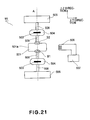
- the optical deflector 95 used here is shown in FIG. 21 .
- the optical deflector 95 comprises a movable plate (hereinafter, “first movable plate”) 501, two movable plates (hereinafter, “second movable plate”) 504 provided above and below (along Z-direction or sub-scan direction) the first movable plate 501, and a mechanical grounding and supporting member 505. It furthermore comprises a torsion spring 508 which provides elastic support for these elements.
- the driving means 506 comprises a fixed magnetic coil. In response to an arbitrary electric current from a drive control means 507, the driving means produces oscillation based on the electromagnetic force caused with a magnet 503 mounted on the second movable plate 504.
- the first movable plate 501 has a deflecting surface 501a for deflecting light, and it scanningly deflects the light beam from the light source means 91 based on the torsional oscillation of the first movable plate 501 and the second movable plate 504.
- the resonance type optical deflector 95 illustrated in FIG. 21 is a dual-freedom oscillation system which is configured, when driven by superimposing a frequency twofold the reference frequency upon the reference frequency, to accomplish scanning deflection having a wider constant angular-speed region as compared with a sinusoidal vibration type.
- No. 1 Japanese Laid-Open Patent Application No. 2005-308863
- optical scanning devices with a resonance type optical deflector 95 having been proposed conventionally involve some inconveniences to be described below.
- the deflecting surface 501a thereof receives a large angular acceleration due to torsional oscillation within a predetermined angular range.
- the deflecting surface 501a receives an inertial force by the self-weight at the time of driving, and the deflecting surface 501a flexes largely.
- the deflecting surface 501a deforms due to dynamic flexure, the light beam reflected by the deflecting surface 501a will produce wavefront aberration (comatic aberration) of a quantity twofold the amount of deformation. This will adversely affect the imaging spot produced on the surface of a photosensitive drum 8.
- the wavefront aberration (comatic aberration) producing by dynamic flexure may be corrected by using an imaging optical system LB which may be provided between the optical deflector 5 and the photosensitive drum surface 8.
- the quantity of correction based on the imaging optical system LB is limited. If the quantity of flexure itself is too large, the correction will be insufficient and the image quality will be degraded.
- the present invention provides a small-size optical scanning device by which deterioration of the wavefront aberration due to dynamic flexure of the deflecting surface of a resonance type optical deflector can be reduced, and an image forming apparatus having such optical scanning device.
- an optical scanning device comprising: a condensing optical system configured to collect a light beam emitted from light source means; deflecting means configured to scanningly deflect the light beam collected by said condensing optical system; and an imaging optical system configured to image the light beam scanningly deflected by said deflecting means, on a surface to be scanned; wherein said deflecting means has a deflecting surface configured to reciprocally move within a main-scan sectional plane and to scanningly deflect the light beam from said condensing optical system, wherein, when said deflecting surface reciprocally moves within the main-scan sectional plane, said deflecting surface receives an angular acceleration which is able to cause deformation thereof being asymmetric with respect to a sub-scan direction, and wherein said condensing optical system is configured to collect the light beam from said light source means to a region of said deflecting surface which region is at a side of a central line of said deflecting
- the deflecting surface of the deflecting means is supported by a supporting means only at one side in the sub-scan direction, and wherein the light beam collected by the condensing optical system is collected to a region of the deflecting surface at a side of the central line of the deflecting surface in the sub-scan direction which side is opposite to the side where the deflecting surface is supported by the supporting means.
- the condensing optical system may be configured to collect the light beam from the light source means to form a focal line on the deflecting surface, and, when an angle defined between a direction of the focal line of the light beam and a main-scan direction passing through a center of the deflecting surface is denoted by ⁇ (deg.), a relation
- the light beam collected by the condensing optical system when the same is projected in the main-scan sectional plane, may be incident on the deflecting surface from an optical axis direction of the imaging optical system, and the light beam collected by the condensing optical system may be incident within a sub-scan sectional plane at a finite angle with respect to an optical axis of the imaging optical system.
- the deflecting means may include a movable plate having the deflecting surface, and the movable plate may have a thickness not less than 100 ⁇ m and not greater than 500 ⁇ m.
- the deflecting surface of the deflecting means may be driven while a frequency n-fold a reference frequency is superimposed on the reference frequency, where n is an integer.
- an optical scanning device comprising: a condensing optical system configured to collect a light beam emitted from light source means; deflecting means configured to scanningly deflect the light beam collected by said condensing optical system; and an imaging optical system configured to image the light beam scanningly deflected by said deflecting means, on a surface to be scanned; wherein said deflecting means has a deflecting surface configured to reciprocally move within a main-scan sectional plane and to scanningly deflect the light beam from said condensing optical system, wherein said deflecting surface is supported by a supporting member at both sides with respect to a sub-scan direction, and wherein said condensing optical system is configured to collect the light beam from said light source means to a region of said deflecting surface which region is within a range of 0.25xH in the sub-scan direction from a central line of said deflecting surface with respect to the sub-scan direction, where a width of said de
- the condensing optical system is configured to collect the light beam from the light source means to form a focal line on the deflecting surface, and, when an angle defined between a direction of the focal line of the light beam and a main-scan direction passing through a center of the deflecting surface is denoted by ⁇ (deg.), a relation
- the light beam collected by the condensing optical system when the same is projected in the main-scan sectional plane, may be incident on the deflecting surface from an optical axis direction of the imaging optical system, and the light beam collected by the condensing optical system may be incident in a sub-scan sectional plane at a finite angle with respect to an optical axis of the imaging optical system.
- the deflecting means may include a movable plate having the deflecting surface, and the movable plate may have a thickness not less than 100 ⁇ m and not greater than 500 ⁇ m.
- the deflecting surface of the deflecting means may be driven while a frequency n-fold a reference frequency is superimposed on the reference frequency, where n is an integer.
- an image forming apparatus comprising: an optical scanning device as recited above; a photosensitive member disposed at a surface to be scanned; a developing device for developing an electrostatic latent image formed on said photosensitive member with a light beam scanningly deflected by said optical scanning device, to produce a toner image; a transferring device for transferring the developed toner image onto a transfer material; and a fixing device for fixing the transferred toner image, on the transfer material.
- an image forming apparatus comprising: an optical scanning device as recited above; and a printer controller for converting code data supplied from an outside machine into an imagewise signal and for inputting the imagewise signal into said optical scanning device.
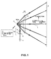
- FIG. 1 a sectional view (main-scan sectional view), in the main-scan direction, of a main portion of a first embodiment of the present invention.
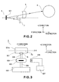
- FIG. 2 is a sectional view (sub-scan sectional view), in the sub-scan direction, of a main portion of the first embodiment of the present invention.
- main-scan direction refers to a direction (Y direction) which is perpendicular to the oscillation axis of deflecting means and the optical axis (X direction) of an imaging optical system (i.e. the direction in which the light beam is scanningly deflected (scanningly reflected) by the deflecting means).
- sub-scan direction refers to a direction (Z direction) which is parallel to the oscillation axis of the deflecting means.
- main-scan section refers to a plane which contains the main-scan direction and the optical axis of the imaging optical system.
- sub-scan section refers to a section which is perpendicular to main-scan section.
- Denoted in the diagram at 1 is light source means, and it comprises a semiconductor laser.
- Denoted at 2 is an aperture stop, and it restricts the light beam (light quantity) passing therethrough.
- Denoted at 3 is a condenser lens (a collimator lens), and it functions to transform a divergent light beam emitted from the light source means 1 into a parallel light beam.
- Denoted at 4 is a cylindrical lens, and it has a refracting power only in the sub-scan direction (sub-scan section).
- the cylindrical lens 4 functions to image the light beam passed through the collimator lens 3, within sub-scan section, into a line image (focal line) upon the deflecting surface 501a of an optical deflector 5 to be described below.
- collimator lens 3 and the cylindrical lens 4 may be replaced by a single optical element (anamorphic lens).
- Denoted at 7 is a reflecting mirror which reflects the light beam toward the optical deflector 5 side.
- the aperture stop 2, collimator lens 3, cylindrical lens 4 and reflecting mirror 7 are components of a condensing optical system (input optical system) LA.
- Denoted at 5 is an optical deflector of resonance type as deflecting means, and it comprises a galvanometer mirror (oscillating mirror).
- the optical deflector 5 has a deflecting surface (deflective reflection surface) 501a which moves reciprocally to deflectively reflect the light beam.
- the condensing optical system LA functions to collect the light beam from the light source means 1 to form a focal line on the deflecting surface.
- Denoted at LB is an imaging optical system having an f ⁇ characteristic, and it is comprised of a single imaging lens (f ⁇ lens) 6 made of a plastic material.
- the imaging optical system LB serves to image the light beam deflected by the optical deflector 5, on the surface 8 to be scanned (photosensitive member surface). Also with respect to the sub-scan section, it functions to provide a conjugate relationship between the deflecting surface 501a and the photosensitive drum surface 8, to thereby perform surface tilt correction.
- Denoted at 8 is a photosensitive drum surface which is the surface to be scanned.
- the divergent light beam from the semiconductor laser 1 being optically modulated in accordance with imagewise information goes through the aperture stop 2 by which the light quantity is restricted.
- the light beam is then transformed into a parallel light beam by means of the collimator lens 3, and then it is incident on the cylindrical lens 4.
- the light passing through this cylindrical lens 4 is incident on the deflecting surface 501a via the reflecting mirror 7, from the center of the deflection angle of the optical deflector 5 (front incidence).
- the light beam from the condensing optical system LA when the same is projected within the main-scan section, is incident on the deflecting surface 501a from the optical axis direction of the imaging optical system LB (oblique incidence optical system).
- the light beam is incident at a finite angle with respect to the optical axis L of the imaging optical system LB.
- the light beam deflectively reflected by the deflecting surface 501a of the optical deflector 5 is directed onto the photosensitive drum surface 8 through the imaging optical system 6.
- the photosensitive drum surface 8 is optically scanned in a predetermined direction (main-scan direction).
- image recording is carried out on the photosensitive drum surface 8 as a recording medium.
- the tilt amount in the sub-scan direction is different depending on the deflection angle, this being attributable to the installation precision error of the magnet 503 shown in FIG. 3 , to be described later.
- the deflecting surface 501a and the photosensitive drum surface 8 should preferably be placed in a conjugate relationship with each other, within the sub-scan section.
- the size of the deflecting surface had better be made small as much as possible.
- the light beam is incident on the deflecting surface 501a of the resonance type optical deflector 5 from the front of the same (front incidence), from the imaging lens 6 side.
- the size (width in the main-scan direction) of the deflecting surface 501a of the resonance type optical deflector 5 can be made smallest, and high-speed oscillation is ensured.
- the light beam going to be incident on the deflecting surface 501a should preferably be incident there while keeping a finite angle with respect to the optical axis L of the imaging optical system LB, within the sub-scan section, as described hereinbefore.
- an oblique incidence angle of ⁇ 3 deg. is given in the sub-scan direction, and the light beam is incident via the reflecting mirror 7 from below in the sub-scan direction (from the above and below with respect to the normal to the deflecting surface 501a, as viewed in the drawing).
- the imaging lens 6 which constitutes the imaging optical system LB is disposed at a predetermined distance upward in the sub-scan direction to ensure that the deflected light beam being deflectively reflected upwardly in the sub-scan direction is incident thereon. Hence, the deflected light beam incident on the imaging lens 6 is imaged on the photosensitive drum 8 as a spot.
- the resonance type optical deflector 5 of the present embodiment is driven while superimposing, on the reference frequency, a frequency twofold of the reference frequency. Based on this, deflective scan having a wider constant angular-speed region as compared with sinusoidal oscillation type is accomplished.
- the spot at the image end portion will expand as compared with that at the image central portion, causing deterioration of the image quality.
- the present embodiment uses a resonance type optical deflector 5 of two-degree-of-freedom system, thereby to widen the constant angular-speed region.
- This enables use of an imaging lens having an f ⁇ characteristic, which has conventionally been used in polygon mirrors.
- FIG. 3 is a schematic diagram of a main portion of a resonance type optical deflector according to the first embodiment of the present invention.
- the optical deflector 5 shown in FIG. 3 comprises a movable plate (first movable plate) 501, a movable plate (the second movable plate) 504 provided below the first movable plate 501 in the sub-scan direction (Z-direction), and a mechanical grounding supporting member 505. Furthermore, it comprises a torsion spring 508 as a supporting member for providing elastic support for these components. Denoted at B is the supporting portion.
- the driving means 506 comprises a fixed magnetic coil. In response to an arbitrary electric currents from drive control means 507, it produces oscillation based on the electromagnetic force caused with a magnet 503 mounted on the second movable plate 504.
- the first movable plate 501 has a deflecting surface 501a for deflecting light and, based on torsional oscillation of the first movable plate 501 and the second movable plate 504, it scanningly deflects the light beam from the light source means 1.
- the drive control means 507 controls the driving means 506 so that the system comprised of the first and second movable plates 501 and 504 and the torsion spring 508 simultaneously oscillates at the reference frequency and a frequency n-fold the reference frequency, where n is an integer.
- the amplitude and phase of the movable plates at the reference frequency and the n-fold frequency thereof may be changed in various ways, to accomplish a variety of driving manners.
- the phases of them have a difference of 180 deg.
- d ⁇ ⁇ 1 dt ⁇ 1 ⁇ ⁇ 1 ⁇ cos ⁇ 1 ⁇ t - ⁇ 2 ⁇ ⁇ 2 ⁇ cos ( ⁇ 2 ⁇ t )
- d 2 ⁇ ⁇ 1 dt 2 - ⁇ 1 ⁇ ⁇ 1 2 ⁇ sin ⁇ 1 ⁇ t + ⁇ 2 ⁇ ⁇ 2 2 ⁇ cos ( ⁇ 2 ⁇ t )
- the axis of abscissas denotes the period T (time) of oscillation
- the axis of ordinate denotes the oscillation angle ⁇ 2 (the unit is degree).
- FIG. 5 is a graph which illustrates the angular speed of the deflection angle of the first movable plate 501.
- the axis of abscissas denotes the period T (time) of oscillation
- the axis of ordinate denotes the angular acceleration. It is seen that the angular acceleration is constant from time 0 to time 0.14T.
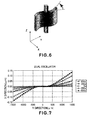
- the thickness of the first movable plate 501 is 200 ⁇ m
- the width thereof in the main-scan direction (Y-direction) is 3.2 mm
- the width thereof in the sub-scan direction (Z-direction) is 1.1 mm.
- FIG. 7 is a graph showing the amount of surface deformation (quantity of dynamic flexure) of the deflecting surface 501a in the state where the image end portion is being scanned, when the oscillation described above is carried out.
- the surface deformation was calculated based on the finite element method.
- FIG. 8 is an enlarged view of the central part of the graph illustrated in FIG. 7 .
- This graph was prepared by detecting the surface deformations at certain heights of the deflecting surface 501a and by removing surface tilt components, at respective heights, at the central portion in the main-scan direction.
- the amount of surface deformation is larger in the region at the side (Z ⁇ 0, below the central line Z0 shown in FIG. 3 ) where the deflecting surface 501a is supported by the torsion spring 508, and that the amount of surface deformation is smaller in the region at the other side (Z>0, above the central line Z0 in FIG. 3 ).
- the surface deformation is larger at the supported side and it is smaller at the non-supported side.
- the thickness of the first movable plate 501 of the present embodiment is 200 ⁇ m, in order to reduce dynamic flexure thereof due to the angular acceleration, the thickness may be enlarged.
- the length of the torsion spring 508 has to be prolonged.
- the size itself of the resonance type optical deflector has to be enlarged, and it causes increase in size of the overall optical scanning device.
- the thickness of the first movable plate 501 is made smaller, the size itself of the resonance type optical deflector 5 will be smaller. However, the amount of dynamic flexure described hereinbefore becomes large, and the spot to be imaged on the scanned surface is affected thereby.
- the thickness of the first movable plate 501 should preferably be set in the range not less than 100 ⁇ m and not greater than 500 ⁇ m.
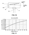
- the upper region (above the central line Z0) where the amount of deformation is smaller is selected, and the focal line 510 is set in that region.
- the condensing optical system LA collects the light beam emitted from the light source means 1, within range of the deflecting surface 501a in the sub-scan direction, and specifically to the region which is at a side of the central line Z0 (above the central line Z0) with respect to the sub-scan direction, where, of the asymmetric deformation of the deflecting surface 501a in the sub-scan direction, the deformation amount is smaller.
- the difficulty of designing the imaging optical system LB is different between a case using the upper region (region above the central line Z0) having smaller surface deformation and a case using the lower region (region below the central line Z0) having larger surface deformation.
- the optical designing is naturally easier when the upper region having smaller surface deformation is used.
- the influence of the surface deformation can be lowered by defining the focal line 510 at a side opposite to the supported side.
- the influence of the surface deformation is lowered by collecting the light beam condensed by the condensing optical system LA to the region of the deflecting surface 501a which region is at a side of the central line A0 in the sub-scan direction, opposite to the side being supported by the supporting member 508.
- the focal line can be set away from the local surface deformation (at region B shown in FIG. 9 ).
- a vertically symmetrical surface deformation will be produced if the resonance type optical deflector uses a movable plate or torsional spring having a vertically asymmetrical shape.
- the focal line may be defined at a side of the central portion of the movable plate with respect to the height direction of the movable plate where deformation is smaller, by which the influence of the surface deformation on the spot can be reduced.
- the influence on the spot will apparently become smaller by defining the focal line 510 in the region where the surface deformation is smaller.
- FIG. 11 is a graph wherein the position (position in the sub-scan direction) of deflecting surface 501a in the height direction is taken on the axis of abscissas, while the tilt component of the deflecting surface at the central portion in the main-scan direction is taken on the axis of ordinate.
- tilt angle tilt angle
- ⁇ deg.
- the value thereof should preferably be 1 deg. or less.
- ⁇ the angle defined between the focal line direction of the light beam and the main-scan direction (Y-direction) passing through the center of the deflecting surface 501a.
- the quantity of wavefront aberration is kept in the range allowed with respect to the design.
- conditional expression (1) had better be set as follows. ⁇ ⁇ 0.2 deg .
- the imaging optical system LB is constituted by a single lens in the present embodiment, the invention is not limited to this. It may be constituted by two ore more pieces of lenses. Furthermore, the imaging optical system LB may include a diffractive optical element.
- FIG. 12 is a schematic diagram of a main portion of a resonance type optical deflector according to a second embodiment of the present invention.
- FIG. 12 like numerals are assigned to components corresponding to those of FIG. 9 .
- the present embodiment differs from the abovementioned first embodiment in that both sides of the first movable plate 501 in the sub-scan direction (Z-direction) are supported by torsion springs 508 and that second movable plates 504 are provided at both sides of the first movable plate 501 in the sub-scan direction.
- Denoted in FIG. 12 at 500 is an optical deflector of resonance type as deflecting means, and it comprises a galvanometer mirror (oscillating mirror).
- FIG. 13 is a graph showing the amount of surface deformation (quantity of dynamic flexure) of the deflecting surface 501a in the state where the image end portion is being scanned, when the oscillation the same as that of the first embodiment is carried out.
- the surface deformation was calculated based on the finite element method.
- FIG. 14 is an enlarged view of the central part of the graph illustrated in FIG. 13 .
- This graph was prepared by detecting the surface deformations at certain heights of the deflecting surface 501a and by removing surface tilt components, at respective heights, at the central portion in the main-scan direction.
- the resonance type optical deflector 500 used in the present embodiment has a vertically symmetry shape with respect to the central line Z0, only the data concerning the upper side of the first movable plate 501 is plotted in the graph.
- the spot to be imaged on the photosensitive drum surface 8 will be deformed largely, and thus high-quality image formation will be difficult to attain.
- the focal line had better be defined while avoiding the region where local deformation occurs.
- the initial focal line position within the range of 0.25xH from the central line Z0, while taking into account the possibility that the position of the focal line 510 shifts relative to the central line Z0 upwardly or downwardly due to any environmental variation.
- the condensing optical system LA collects the light beam from the light source means 1 in the range of the deflecting surface 501a, specifically, to the region of the deflecting surface 501a which region is within a range of 0.25xH in the sub-scan direction from a central line Z0 of the deflecting surface with respect to the sub-scan direction.
- the light beam emitted from the light source means 1 had better be condensed into the region in the range of 0.1xH ⁇ m in the sub-scan direction, from the central line Z0 in the sub-scan direction.
- the surface deformation shown in FIG. 13 and FIG. 14 should preferably be considered while taking into account the difference of tilt component at the central portion in the main-scan direction.
- the value of tilt component (tilt angle) ⁇ of the focal line 510 should preferably be set to 1 deg. or less.
- FIG. 17 is a sectional view (sub-scan sectional view) in the sub-scan direction of a main portion, for explaining the method of adjusting the focal line position in a third embodiment of the present invention.
- FIG. 17 like numerals are assigned to components corresponding to those of FIG. 1 .
- the focal line 510 can be shifted to a particular position by moving the cylindrical lens 4 shown FIG. 17 in the direction of an arrow C (sub-scan direction).
- the focal line 510 can be shifted to a particular position even by moving the resonance type optical deflector 5 itself in the direction of an arrow D.
- the adjustment may be made by relatively moving the cylindrical lens 4 and the optical deflector 5.
- the focal line 510 can be shifted to a particular position even by rotating the cylindrical lens 4 n the direction of an arrow E around the optical axis X.
- the focal line 510 can be shifted to a particular position even by rotating the resonance type optical deflector itself in the direction of an arrow F shown in the drawing.
- the adjustment may be made by relatively rotating the cylindrical lens 4 and the optical deflector 5.
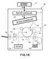
- Figure 18 is a schematic and sectional view, in the sub-scan direction, of a main portion of an image forming apparatus according to an embodiment of the present invention.
- Denoted generally at 104 in the drawing is the image forming apparatus.
- the image forming apparatus 104 receives code data Dc supplied thereto from an external machine 117 such as a personal computer, for example.
- the code data Dc is then transformed by a printer controller 111 inside the apparatus, into imagewise data (dot data) Di.
- the imagewise data Di is then inputted into an optical scanning unit 100 which is configured in accordance with any one of the preceding embodiments described hereinbefore.
- the optical scanning unit 100 produces a light beam 103 having been modulated in accordance with the imagewise data Di, and with this light beam 103, the photosensitive surface of a photosensitive drum 101 is scanned in the main-scan direction.
- the photosensitive drum 101 which is an electrostatic latent image bearing member (photosensitive member) is rotated clockwise by means of a motor 115. Through this rotation, the photosensitive surface of the photosensitive drum 101 is moved relatively to the light beam 103, in the sub-scan direction which is orthogonal to the main-scan direction.
- a charging roller 102 Disposed just above the photosensitive drum 101 is a charging roller 102 which is in contact with the photosensitive drum surface to electrically charge the drum surface uniformly. Onto the photosensitive drum 101 surface having been electrically charged by the charging roller 102, the light beam 103 being scanned by the optical scanning unit 100 is projected.
- the light beam 103 has been modulated in accordance with the imagewise data Di.
- an electrostatic latent image is formed on the photosensitive drum 101 surface.
- the electrostatic latent image thus formed is then developed into a toner image, by means of a developing device 107 which is provided at a position downstream of the irradiation position of the light beam 103 with respect to the rotational direction of the photosensitive drum 101 and which is in contact with the photosensitive drum 101.
- the toner image thus developed by the developing device 107 is transferred onto a transfer sheet (transfer material) 112 below the photosensitive drum 101, by means of a transfer roller 108 which is disposed opposed to the photosensitive drum 101.
- Transfer sheets 112 are stored in a sheet cassette 109 in front of (at the right-hand side as viewed in Figure 15 ) the photosensitive drum, but these can be supplied manually.
- a sheet supplying roller 110 at an end portion of the sheet cassette 109, for supplying each sheet 112 in the cassette 109 into a sheet supply path.
- the paper sheet 112 having an unfixed toner image transferred thereto in the manner described above is conveyed to a fixing device behind (at the left-hand side as viewed in Figure 15 ) the photosensitive drum 101.
- the fixing device comprises a fixing roller 113 having a built-in fixing heater (not shown) and a pressing roller 114 disposed to be press-contacted to the fixing roller 113.
- the transfer sheet 112 supplied from the image transfer station is heated under pressure at the press contact area between the fixing roller 113 and the pressing roller 114, whereby the unfixed toner image on the transfer sheet 112 is fixed thereon.
- the print controller 111 has various functions in addition to the data conversion function described hereinbefore, such as for controlling a motor 115 or any other components inside the image forming apparatus as well as a polygon motor inside the optical scanning unit (to be described later).
- the recording density of the image forming apparatus there is no particular limitation with regard to the recording density of the image forming apparatus to be used in the present invention.
- the structures according to the first and second embodiments of the present invention will be more effective when they are introduced into an image forming apparatus of a resolution 1200 dpi or higher.
- Figure 19 is a schematic view of a main portion of a color image forming apparatus according to an embodiment of the present invention.
- This embodiment is directed to a tandem type color image forming apparatus in which four optical scanning devices are provided so as to record imagewise data upon the surfaces of corresponding photosensitive drums (image bearing members) in parallel to each other.
- FIG 19 denoted generally at 60 is a color image forming apparatus, and denoted at 11, 12, 13 and 14 are optical scanning devices having a structure according to any one of the preceding embodiments.
- Denoted at 21, 22, 23 and 24 are photosensitive drums (image bearing members), and denoted at 31, 32, 33 and 34 are developing devices, respectively.
- Denoted at 51 is a conveyance belt.
- the image forming apparatus further comprises a transfer device for transferring the toner image developed by the developing device to a transfer material, and a fixing device for fixing the transferred toner image on the transfer sheet.
- the color image forming apparatus 60 receives color signals of R (red), G (green) and B (blue) supplied thereto from an outside machine 52 such as a personal computer, for example. These color signals are transformed by means of a printer controller 53 inside the image forming apparatus, into imagewise data (dot data) corresponding to C (cyan), M (magenta), Y (yellow) and B (black).
- optical scanning devices 11, 12, 13 and 14, respectively These imagewise data are inputted into the optical scanning devices 11, 12, 13 and 14, respectively.
- these optical scanning devices produce light beams 41, 42, 43 and 44 having been modulated in accordance with the associated imagewise data.
- the photosensitive surfaces of the photosensitive drums 21, 22, 23 and 24 are scanned in the main-scan direction.
- optical scanning devices 11, 12, 13 and 14 are provided and these correspond to colors of C (cyan), M (magenta), Y (yellow) and B (black), respectively. These scanning devices are operable in parallel to each other to record imagewise signals upon the surfaces of the photosensitive drums 21, 22, 23 and 24, respectively, so that a color image can be printed at high speed.
- the color image forming apparatus of this embodiment uses four optical scanning devices 11, 12, 13 and 14 to produce latent images for different colors upon the surfaces of corresponding photosensitive drums 21, 22, 23 and 24, respectively, by use of light beams based on respective image data. After that, these images are superposedly transferred onto a recording sheet, whereby a single full-color image is produced thereon.
- a color image reading machine having a CCD sensor may be used. In that occasion, this color image reading machine and the color image forming apparatus 60 will provide a color digital copying machine.
Landscapes
- Physics & Mathematics (AREA)
- General Physics & Mathematics (AREA)
- Optics & Photonics (AREA)
- Engineering & Computer Science (AREA)
- Computer Vision & Pattern Recognition (AREA)
- Facsimile Scanning Arrangements (AREA)
- Laser Beam Printer (AREA)
- Mechanical Optical Scanning Systems (AREA)
Applications Claiming Priority (1)
| Application Number | Priority Date | Filing Date | Title |
|---|---|---|---|
| JP2007033462A JP2008197452A (ja) | 2007-02-14 | 2007-02-14 | 光走査装置及びそれを用いた画像形成装置 |
Publications (2)
| Publication Number | Publication Date |
|---|---|
| EP1959293A1 true EP1959293A1 (de) | 2008-08-20 |
| EP1959293B1 EP1959293B1 (de) | 2013-05-01 |
Family
ID=39301309
Family Applications (1)
| Application Number | Title | Priority Date | Filing Date |
|---|---|---|---|
| EP08002640.4A Not-in-force EP1959293B1 (de) | 2007-02-14 | 2008-02-13 | Optische Abtastvorrichtung und Bilderzeugungsvorrichtung damit |
Country Status (5)
| Country | Link |
|---|---|
| US (1) | US7911669B2 (de) |
| EP (1) | EP1959293B1 (de) |
| JP (1) | JP2008197452A (de) |
| KR (1) | KR100954906B1 (de) |
| CN (1) | CN101251646B (de) |
Families Citing this family (2)
| Publication number | Priority date | Publication date | Assignee | Title |
|---|---|---|---|---|
| CN109491077B (zh) | 2018-12-29 | 2020-11-17 | 珠海奔图电子有限公司 | 光学扫描设备和电子成像装置 |
| US12487448B2 (en) * | 2021-12-06 | 2025-12-02 | Brother Kogyo Kabushiki Kaisha | Scanning optical device |
Citations (1)
| Publication number | Priority date | Publication date | Assignee | Title |
|---|---|---|---|---|
| US20050243396A1 (en) * | 2004-04-12 | 2005-11-03 | Mitsumi Fujii | Deflector mirror, optical scanning device, and image forming apparatus |
Family Cites Families (8)
| Publication number | Priority date | Publication date | Assignee | Title |
|---|---|---|---|---|
| JP2002048993A (ja) * | 2000-05-25 | 2002-02-15 | Canon Inc | 光走査装置及びそれを用いた画像形成装置 |
| JP3507474B2 (ja) * | 2001-01-11 | 2004-03-15 | キヤノン株式会社 | 光走査装置及びそれを用いた画像形成装置 |
| US6972883B2 (en) | 2002-02-15 | 2005-12-06 | Ricoh Company, Ltd. | Vibration mirror, optical scanning device, and image forming using the same, method for making the same, and method for scanning image |
| US6840642B2 (en) * | 2002-06-28 | 2005-01-11 | Sony Corporation | Thermally actuated micro mirror and electronic device |
| JP2005024722A (ja) | 2003-06-30 | 2005-01-27 | Ricoh Co Ltd | 振動ミラー、光走査装置および画像形成装置 |
| JP4370905B2 (ja) * | 2003-12-26 | 2009-11-25 | セイコーエプソン株式会社 | 光走査装置および画像形成装置 |
| JP4416117B2 (ja) | 2004-04-19 | 2010-02-17 | 株式会社リコー | 偏向ミラー、光走査装置及び画像形成装置 |
| JP2006178408A (ja) | 2004-11-25 | 2006-07-06 | Ricoh Co Ltd | スキャナ素子、光走査装置および画像形成装置 |
-
2007
- 2007-02-14 JP JP2007033462A patent/JP2008197452A/ja active Pending
-
2008
- 2008-02-07 US US12/028,010 patent/US7911669B2/en not_active Expired - Fee Related
- 2008-02-13 EP EP08002640.4A patent/EP1959293B1/de not_active Not-in-force
- 2008-02-14 CN CN2008100056463A patent/CN101251646B/zh not_active Expired - Fee Related
- 2008-02-14 KR KR1020080013310A patent/KR100954906B1/ko not_active Expired - Fee Related
Patent Citations (1)
| Publication number | Priority date | Publication date | Assignee | Title |
|---|---|---|---|---|
| US20050243396A1 (en) * | 2004-04-12 | 2005-11-03 | Mitsumi Fujii | Deflector mirror, optical scanning device, and image forming apparatus |
Also Published As
| Publication number | Publication date |
|---|---|
| EP1959293B1 (de) | 2013-05-01 |
| JP2008197452A (ja) | 2008-08-28 |
| CN101251646B (zh) | 2011-08-24 |
| CN101251646A (zh) | 2008-08-27 |
| KR20080076786A (ko) | 2008-08-20 |
| KR100954906B1 (ko) | 2010-04-27 |
| US20080192324A1 (en) | 2008-08-14 |
| US7911669B2 (en) | 2011-03-22 |
Similar Documents
| Publication | Publication Date | Title |
|---|---|---|
| JP5228331B2 (ja) | 光走査装置、画像形成装置、および多色対応の画像形成装置 | |
| EP1450198B1 (de) | Scanner | |
| US20080151326A1 (en) | Optical scanning device and image forming apparatus using the same | |
| JP5170983B2 (ja) | 光偏向器、及びそれを用いた光学機器 | |
| JP4146177B2 (ja) | 光走査装置および画像形成装置 | |
| JP5164345B2 (ja) | 光走査装置及びそれを用いた画像形成装置 | |
| EP1959293B1 (de) | Optische Abtastvorrichtung und Bilderzeugungsvorrichtung damit | |
| JP4689462B2 (ja) | 光走査装置・画像形成装置 | |
| CN100470300C (zh) | 光学扫描系统以及使用其的成像设备 | |
| US7646523B2 (en) | Optical scanning apparatus and image forming apparatus using same | |
| JP2010122248A (ja) | 光走査装置および画像形成装置 | |
| JP2006251513A (ja) | 光源装置、光走査装置および画像形成装置 | |
| JP4701593B2 (ja) | 光走査装置および画像形成装置 | |
| EP1895350A1 (de) | Optische Abtastvorrichtung und Bilderzeugungsvorrichtung damit | |
| JP2011257696A (ja) | 光走査装置及び画像形成装置 | |
| JP4458833B2 (ja) | 光走査装置および画像形成装置 | |
| JP5034094B2 (ja) | 光走査装置、および画像形成装置 | |
| JP2009031317A (ja) | 光走査装置及びそれを用いた画像形成装置 | |
| JP2010217200A (ja) | 光走査装置および画像形成装置 | |
| KR100854805B1 (ko) | 광주사장치 및 이것을 이용한 화상형성장치 | |
| JP2004287214A (ja) | 露光装置および画像形成装置 | |
| JP2005070708A (ja) | 光走査装置および画像形成装置 | |
| JP2008020481A (ja) | 光走査装置及び画像形成装置 | |
| JP2004287212A (ja) | 画像形成装置 | |
| JP2004287213A (ja) | 露光装置および画像形成装置 |
Legal Events
| Date | Code | Title | Description |
|---|---|---|---|
| PUAI | Public reference made under article 153(3) epc to a published international application that has entered the european phase |
Free format text: ORIGINAL CODE: 0009012 |
|
| AK | Designated contracting states |
Kind code of ref document: A1 Designated state(s): AT BE BG CH CY CZ DE DK EE ES FI FR GB GR HR HU IE IS IT LI LT LU LV MC MT NL NO PL PT RO SE SI SK TR |
|
| AX | Request for extension of the european patent |
Extension state: AL BA MK RS |
|
| 17P | Request for examination filed |
Effective date: 20090220 |
|
| AKX | Designation fees paid |
Designated state(s): AT BE BG CH CY CZ DE DK EE ES FI FR GB GR HR HU IE IS IT LI LT LU LV MC MT NL NO PL PT RO SE SI SK TR |
|
| 17Q | First examination report despatched |
Effective date: 20090406 |
|
| GRAP | Despatch of communication of intention to grant a patent |
Free format text: ORIGINAL CODE: EPIDOSNIGR1 |
|
| GRAS | Grant fee paid |
Free format text: ORIGINAL CODE: EPIDOSNIGR3 |
|
| GRAA | (expected) grant |
Free format text: ORIGINAL CODE: 0009210 |
|
| AK | Designated contracting states |
Kind code of ref document: B1 Designated state(s): AT BE BG CH CY CZ DE DK EE ES FI FR GB GR HR HU IE IS IT LI LT LU LV MC MT NL NO PL PT RO SE SI SK TR |
|
| REG | Reference to a national code |
Ref country code: GB Ref legal event code: FG4D |
|
| REG | Reference to a national code |
Ref country code: AT Ref legal event code: REF Ref document number: 610273 Country of ref document: AT Kind code of ref document: T Effective date: 20130515 Ref country code: CH Ref legal event code: EP |
|
| REG | Reference to a national code |
Ref country code: IE Ref legal event code: FG4D |
|
| REG | Reference to a national code |
Ref country code: DE Ref legal event code: R082 Ref document number: 602008024196 Country of ref document: DE Representative=s name: WESER & KOLLEGEN, DE |
|
| REG | Reference to a national code |
Ref country code: DE Ref legal event code: R096 Ref document number: 602008024196 Country of ref document: DE Effective date: 20130627 |
|
| REG | Reference to a national code |
Ref country code: AT Ref legal event code: MK05 Ref document number: 610273 Country of ref document: AT Kind code of ref document: T Effective date: 20130501 |
|
| REG | Reference to a national code |
Ref country code: NL Ref legal event code: VDEP Effective date: 20130501 |
|
| REG | Reference to a national code |
Ref country code: LT Ref legal event code: MG4D |
|
| PG25 | Lapsed in a contracting state [announced via postgrant information from national office to epo] |
Ref country code: AT Free format text: LAPSE BECAUSE OF FAILURE TO SUBMIT A TRANSLATION OF THE DESCRIPTION OR TO PAY THE FEE WITHIN THE PRESCRIBED TIME-LIMIT Effective date: 20130501 Ref country code: FI Free format text: LAPSE BECAUSE OF FAILURE TO SUBMIT A TRANSLATION OF THE DESCRIPTION OR TO PAY THE FEE WITHIN THE PRESCRIBED TIME-LIMIT Effective date: 20130501 Ref country code: GR Free format text: LAPSE BECAUSE OF FAILURE TO SUBMIT A TRANSLATION OF THE DESCRIPTION OR TO PAY THE FEE WITHIN THE PRESCRIBED TIME-LIMIT Effective date: 20130802 Ref country code: IS Free format text: LAPSE BECAUSE OF FAILURE TO SUBMIT A TRANSLATION OF THE DESCRIPTION OR TO PAY THE FEE WITHIN THE PRESCRIBED TIME-LIMIT Effective date: 20130901 Ref country code: NO Free format text: LAPSE BECAUSE OF FAILURE TO SUBMIT A TRANSLATION OF THE DESCRIPTION OR TO PAY THE FEE WITHIN THE PRESCRIBED TIME-LIMIT Effective date: 20130801 Ref country code: PT Free format text: LAPSE BECAUSE OF FAILURE TO SUBMIT A TRANSLATION OF THE DESCRIPTION OR TO PAY THE FEE WITHIN THE PRESCRIBED TIME-LIMIT Effective date: 20130902 Ref country code: LT Free format text: LAPSE BECAUSE OF FAILURE TO SUBMIT A TRANSLATION OF THE DESCRIPTION OR TO PAY THE FEE WITHIN THE PRESCRIBED TIME-LIMIT Effective date: 20130501 Ref country code: ES Free format text: LAPSE BECAUSE OF FAILURE TO SUBMIT A TRANSLATION OF THE DESCRIPTION OR TO PAY THE FEE WITHIN THE PRESCRIBED TIME-LIMIT Effective date: 20130812 Ref country code: SE Free format text: LAPSE BECAUSE OF FAILURE TO SUBMIT A TRANSLATION OF THE DESCRIPTION OR TO PAY THE FEE WITHIN THE PRESCRIBED TIME-LIMIT Effective date: 20130501 Ref country code: SI Free format text: LAPSE BECAUSE OF FAILURE TO SUBMIT A TRANSLATION OF THE DESCRIPTION OR TO PAY THE FEE WITHIN THE PRESCRIBED TIME-LIMIT Effective date: 20130501 |
|
| PG25 | Lapsed in a contracting state [announced via postgrant information from national office to epo] |
Ref country code: BG Free format text: LAPSE BECAUSE OF FAILURE TO SUBMIT A TRANSLATION OF THE DESCRIPTION OR TO PAY THE FEE WITHIN THE PRESCRIBED TIME-LIMIT Effective date: 20130801 Ref country code: PL Free format text: LAPSE BECAUSE OF FAILURE TO SUBMIT A TRANSLATION OF THE DESCRIPTION OR TO PAY THE FEE WITHIN THE PRESCRIBED TIME-LIMIT Effective date: 20130501 Ref country code: CY Free format text: LAPSE BECAUSE OF FAILURE TO SUBMIT A TRANSLATION OF THE DESCRIPTION OR TO PAY THE FEE WITHIN THE PRESCRIBED TIME-LIMIT Effective date: 20130501 Ref country code: HR Free format text: LAPSE BECAUSE OF FAILURE TO SUBMIT A TRANSLATION OF THE DESCRIPTION OR TO PAY THE FEE WITHIN THE PRESCRIBED TIME-LIMIT Effective date: 20130501 |
|
| PG25 | Lapsed in a contracting state [announced via postgrant information from national office to epo] |
Ref country code: LV Free format text: LAPSE BECAUSE OF FAILURE TO SUBMIT A TRANSLATION OF THE DESCRIPTION OR TO PAY THE FEE WITHIN THE PRESCRIBED TIME-LIMIT Effective date: 20130501 |
|
| PG25 | Lapsed in a contracting state [announced via postgrant information from national office to epo] |
Ref country code: EE Free format text: LAPSE BECAUSE OF FAILURE TO SUBMIT A TRANSLATION OF THE DESCRIPTION OR TO PAY THE FEE WITHIN THE PRESCRIBED TIME-LIMIT Effective date: 20130501 Ref country code: SK Free format text: LAPSE BECAUSE OF FAILURE TO SUBMIT A TRANSLATION OF THE DESCRIPTION OR TO PAY THE FEE WITHIN THE PRESCRIBED TIME-LIMIT Effective date: 20130501 Ref country code: CZ Free format text: LAPSE BECAUSE OF FAILURE TO SUBMIT A TRANSLATION OF THE DESCRIPTION OR TO PAY THE FEE WITHIN THE PRESCRIBED TIME-LIMIT Effective date: 20130501 Ref country code: BE Free format text: LAPSE BECAUSE OF FAILURE TO SUBMIT A TRANSLATION OF THE DESCRIPTION OR TO PAY THE FEE WITHIN THE PRESCRIBED TIME-LIMIT Effective date: 20130501 Ref country code: DK Free format text: LAPSE BECAUSE OF FAILURE TO SUBMIT A TRANSLATION OF THE DESCRIPTION OR TO PAY THE FEE WITHIN THE PRESCRIBED TIME-LIMIT Effective date: 20130501 |
|
| PG25 | Lapsed in a contracting state [announced via postgrant information from national office to epo] |
Ref country code: RO Free format text: LAPSE BECAUSE OF FAILURE TO SUBMIT A TRANSLATION OF THE DESCRIPTION OR TO PAY THE FEE WITHIN THE PRESCRIBED TIME-LIMIT Effective date: 20130501 Ref country code: IT Free format text: LAPSE BECAUSE OF FAILURE TO SUBMIT A TRANSLATION OF THE DESCRIPTION OR TO PAY THE FEE WITHIN THE PRESCRIBED TIME-LIMIT Effective date: 20130501 Ref country code: NL Free format text: LAPSE BECAUSE OF FAILURE TO SUBMIT A TRANSLATION OF THE DESCRIPTION OR TO PAY THE FEE WITHIN THE PRESCRIBED TIME-LIMIT Effective date: 20130501 |
|
| PLBE | No opposition filed within time limit |
Free format text: ORIGINAL CODE: 0009261 |
|
| STAA | Information on the status of an ep patent application or granted ep patent |
Free format text: STATUS: NO OPPOSITION FILED WITHIN TIME LIMIT |
|
| 26N | No opposition filed |
Effective date: 20140204 |
|
| REG | Reference to a national code |
Ref country code: DE Ref legal event code: R097 Ref document number: 602008024196 Country of ref document: DE Effective date: 20140204 |
|
| PG25 | Lapsed in a contracting state [announced via postgrant information from national office to epo] |
Ref country code: LU Free format text: LAPSE BECAUSE OF FAILURE TO SUBMIT A TRANSLATION OF THE DESCRIPTION OR TO PAY THE FEE WITHIN THE PRESCRIBED TIME-LIMIT Effective date: 20140213 Ref country code: MC Free format text: LAPSE BECAUSE OF FAILURE TO SUBMIT A TRANSLATION OF THE DESCRIPTION OR TO PAY THE FEE WITHIN THE PRESCRIBED TIME-LIMIT Effective date: 20130501 |
|
| REG | Reference to a national code |
Ref country code: CH Ref legal event code: PL |
|
| GBPC | Gb: european patent ceased through non-payment of renewal fee |
Effective date: 20140213 |
|
| PG25 | Lapsed in a contracting state [announced via postgrant information from national office to epo] |
Ref country code: CH Free format text: LAPSE BECAUSE OF NON-PAYMENT OF DUE FEES Effective date: 20140228 Ref country code: LI Free format text: LAPSE BECAUSE OF NON-PAYMENT OF DUE FEES Effective date: 20140228 |
|
| REG | Reference to a national code |
Ref country code: FR Ref legal event code: ST Effective date: 20141031 |
|
| REG | Reference to a national code |
Ref country code: IE Ref legal event code: MM4A |
|
| PG25 | Lapsed in a contracting state [announced via postgrant information from national office to epo] |
Ref country code: IE Free format text: LAPSE BECAUSE OF NON-PAYMENT OF DUE FEES Effective date: 20140213 Ref country code: GB Free format text: LAPSE BECAUSE OF NON-PAYMENT OF DUE FEES Effective date: 20140213 Ref country code: FR Free format text: LAPSE BECAUSE OF NON-PAYMENT OF DUE FEES Effective date: 20140228 |
|
| PGFP | Annual fee paid to national office [announced via postgrant information from national office to epo] |
Ref country code: DE Payment date: 20150228 Year of fee payment: 8 |
|
| PG25 | Lapsed in a contracting state [announced via postgrant information from national office to epo] |
Ref country code: MT Free format text: LAPSE BECAUSE OF FAILURE TO SUBMIT A TRANSLATION OF THE DESCRIPTION OR TO PAY THE FEE WITHIN THE PRESCRIBED TIME-LIMIT Effective date: 20130501 |
|
| PG25 | Lapsed in a contracting state [announced via postgrant information from national office to epo] |
Ref country code: TR Free format text: LAPSE BECAUSE OF FAILURE TO SUBMIT A TRANSLATION OF THE DESCRIPTION OR TO PAY THE FEE WITHIN THE PRESCRIBED TIME-LIMIT Effective date: 20130501 Ref country code: HU Free format text: LAPSE BECAUSE OF FAILURE TO SUBMIT A TRANSLATION OF THE DESCRIPTION OR TO PAY THE FEE WITHIN THE PRESCRIBED TIME-LIMIT; INVALID AB INITIO Effective date: 20080213 |
|
| REG | Reference to a national code |
Ref country code: DE Ref legal event code: R119 Ref document number: 602008024196 Country of ref document: DE |
|
| PG25 | Lapsed in a contracting state [announced via postgrant information from national office to epo] |
Ref country code: DE Free format text: LAPSE BECAUSE OF NON-PAYMENT OF DUE FEES Effective date: 20160901 |