EP1947660A2 - Kontaktlose Leistungsübertragungsspule, tragbares Endgerät und Endgerätladevorrichtung, Flachspulenvorrichtung zur Bildung einer Magnetschicht und Verfahren zur Bildung einer Magnetschicht - Google Patents
Kontaktlose Leistungsübertragungsspule, tragbares Endgerät und Endgerätladevorrichtung, Flachspulenvorrichtung zur Bildung einer Magnetschicht und Verfahren zur Bildung einer Magnetschicht Download PDFInfo
- Publication number
- EP1947660A2 EP1947660A2 EP08250066A EP08250066A EP1947660A2 EP 1947660 A2 EP1947660 A2 EP 1947660A2 EP 08250066 A EP08250066 A EP 08250066A EP 08250066 A EP08250066 A EP 08250066A EP 1947660 A2 EP1947660 A2 EP 1947660A2
- Authority
- EP
- European Patent Office
- Prior art keywords
- planar coil
- planar
- coil
- magnetic
- magnetic layer
- Prior art date
- Legal status (The legal status is an assumption and is not a legal conclusion. Google has not performed a legal analysis and makes no representation as to the accuracy of the status listed.)
- Granted
Links
Images


Classifications
-
- H—ELECTRICITY
- H01—ELECTRIC ELEMENTS
- H01F—MAGNETS; INDUCTANCES; TRANSFORMERS; SELECTION OF MATERIALS FOR THEIR MAGNETIC PROPERTIES
- H01F38/00—Adaptations of transformers or inductances for specific applications or functions
- H01F38/14—Inductive couplings
-
- H—ELECTRICITY
- H01—ELECTRIC ELEMENTS
- H01F—MAGNETS; INDUCTANCES; TRANSFORMERS; SELECTION OF MATERIALS FOR THEIR MAGNETIC PROPERTIES
- H01F41/00—Apparatus or processes specially adapted for manufacturing or assembling magnets, inductances or transformers; Apparatus or processes specially adapted for manufacturing materials characterised by their magnetic properties
- H01F41/14—Apparatus or processes specially adapted for manufacturing or assembling magnets, inductances or transformers; Apparatus or processes specially adapted for manufacturing materials characterised by their magnetic properties for applying magnetic films to substrates
- H01F41/16—Apparatus or processes specially adapted for manufacturing or assembling magnets, inductances or transformers; Apparatus or processes specially adapted for manufacturing materials characterised by their magnetic properties for applying magnetic films to substrates the magnetic material being applied in the form of particles, e.g. by serigraphy, to form thick magnetic films or precursors therefor
-
- H—ELECTRICITY
- H01—ELECTRIC ELEMENTS
- H01F—MAGNETS; INDUCTANCES; TRANSFORMERS; SELECTION OF MATERIALS FOR THEIR MAGNETIC PROPERTIES
- H01F5/00—Coils
- H01F5/003—Printed circuit coils
-
- H—ELECTRICITY
- H02—GENERATION; CONVERSION OR DISTRIBUTION OF ELECTRIC POWER
- H02J—ELECTRIC POWER NETWORKS; CIRCUIT ARRANGEMENTS OR SYSTEMS FOR SUPPLYING OR DISTRIBUTING ELECTRIC POWER; SYSTEMS FOR STORING ELECTRIC ENERGY
- H02J50/00—Circuit arrangements or systems for wireless supply or distribution of electric power
- H02J50/005—Mechanical details of housing or structure aiming to accommodate the power transfer means, e.g. mechanical integration of coils, antennas or transducers into emitting or receiving devices
-
- H—ELECTRICITY
- H02—GENERATION; CONVERSION OR DISTRIBUTION OF ELECTRIC POWER
- H02J—ELECTRIC POWER NETWORKS; CIRCUIT ARRANGEMENTS OR SYSTEMS FOR SUPPLYING OR DISTRIBUTING ELECTRIC POWER; SYSTEMS FOR STORING ELECTRIC ENERGY
- H02J50/00—Circuit arrangements or systems for wireless supply or distribution of electric power
- H02J50/10—Circuit arrangements or systems for wireless supply or distribution of electric power using inductive coupling
-
- H—ELECTRICITY
- H02—GENERATION; CONVERSION OR DISTRIBUTION OF ELECTRIC POWER
- H02J—ELECTRIC POWER NETWORKS; CIRCUIT ARRANGEMENTS OR SYSTEMS FOR SUPPLYING OR DISTRIBUTING ELECTRIC POWER; SYSTEMS FOR STORING ELECTRIC ENERGY
- H02J50/00—Circuit arrangements or systems for wireless supply or distribution of electric power
- H02J50/60—Circuit arrangements or systems for wireless supply or distribution of electric power responsive to the presence of foreign objects, e.g. detection of living beings
-
- H—ELECTRICITY
- H02—GENERATION; CONVERSION OR DISTRIBUTION OF ELECTRIC POWER
- H02J—ELECTRIC POWER NETWORKS; CIRCUIT ARRANGEMENTS OR SYSTEMS FOR SUPPLYING OR DISTRIBUTING ELECTRIC POWER; SYSTEMS FOR STORING ELECTRIC ENERGY
- H02J7/00—Circuit arrangements for charging or discharging batteries or for supplying loads from batteries
- H02J7/40—Circuit arrangements for charging or discharging batteries or for supplying loads from batteries characterised by the exchange of charge or discharge related data
- H02J7/47—Arrangements for checking compatibility or authentication between one component, e.g. a battery or a battery charger, and another component, e.g. a power source
-
- H—ELECTRICITY
- H01—ELECTRIC ELEMENTS
- H01F—MAGNETS; INDUCTANCES; TRANSFORMERS; SELECTION OF MATERIALS FOR THEIR MAGNETIC PROPERTIES
- H01F27/00—Details of transformers or inductances, in general
- H01F27/24—Magnetic cores
-
- H—ELECTRICITY
- H01—ELECTRIC ELEMENTS
- H01F—MAGNETS; INDUCTANCES; TRANSFORMERS; SELECTION OF MATERIALS FOR THEIR MAGNETIC PROPERTIES
- H01F27/00—Details of transformers or inductances, in general
- H01F27/28—Coils; Windings; Conductive connections
- H01F27/2871—Pancake coils
-
- Y—GENERAL TAGGING OF NEW TECHNOLOGICAL DEVELOPMENTS; GENERAL TAGGING OF CROSS-SECTIONAL TECHNOLOGIES SPANNING OVER SEVERAL SECTIONS OF THE IPC; TECHNICAL SUBJECTS COVERED BY FORMER USPC CROSS-REFERENCE ART COLLECTIONS [XRACs] AND DIGESTS
- Y10—TECHNICAL SUBJECTS COVERED BY FORMER USPC
- Y10T—TECHNICAL SUBJECTS COVERED BY FORMER US CLASSIFICATION
- Y10T29/00—Metal working
- Y10T29/49—Method of mechanical manufacture
- Y10T29/49002—Electrical device making
- Y10T29/4902—Electromagnet, transformer or inductor
- Y10T29/49073—Electromagnet, transformer or inductor by assembling coil and core
-
- Y—GENERAL TAGGING OF NEW TECHNOLOGICAL DEVELOPMENTS; GENERAL TAGGING OF CROSS-SECTIONAL TECHNOLOGIES SPANNING OVER SEVERAL SECTIONS OF THE IPC; TECHNICAL SUBJECTS COVERED BY FORMER USPC CROSS-REFERENCE ART COLLECTIONS [XRACs] AND DIGESTS
- Y10—TECHNICAL SUBJECTS COVERED BY FORMER USPC
- Y10T—TECHNICAL SUBJECTS COVERED BY FORMER US CLASSIFICATION
- Y10T29/00—Metal working
- Y10T29/53—Means to assemble or disassemble
- Y10T29/5313—Means to assemble electrical device
- Y10T29/53165—Magnetic memory device
Definitions
- This invention relates to a noncontact power-transmission coil, portable terminal and terminal charging device, planar coil magnetic layer formation device, and magnetic layer formation method.
- Japanese Patent Application Publication No. 2006-42519 discloses a planar coil as a noncontact power-transmission coil mounted on a portable terminal desired to be thin, such as a mobile phone unit.
- the planar coil is constructed such that an electric wire is formed of a single or twisted wire.
- the surface of the wire is provided with an insulating layer.
- the wire is spirally wound in a substantially same plane.
- this Patent Document also discloses that the formation of a magnetic sheet. That is, a planer coil on the power-transmitting side and a planar coil on the power-receiving side are arranged facing to each other. Then, the counter surface of each coil, which is opposite to the surface facing to the other coil, is entirely covered with a magnetic sheet to prevent undesired radiation with the magnetic field generated from both coils.
- FIG. 1 and FIG. 2 show in summary the construction of a noncontact power-transmission coil 200 employing a spiral-shape planar coil of the related art.
- an electric wire 201 which employs either single wire or twisted wire, is wound in a spiral shape within a single plane.
- An electric wire end portion (for example, the electric wire end portion on the side at the end of the winding) 205 on the outer periphery 203 of the planar coil is drawn to the outside.
- the electric wire end portion (the electric wire end portion at the beginning of the winding, for example) 204 on the inner periphery 202 passes over (or under) an electric wire portion wound into the spiral shape and is drawn to the outside.
- a magnetic sheet 210 is affixed on one planar portion of the planar coil of the noncontact power-transmission coil 200 through an adhesive sheet 211 or similar.
- the other planar portion is affixed, as necessary, to the inner wall or similar of a terminal housing 213 using an adhesive sheet 211 or similar.
- a metal sheet, of aluminum or similar is also affixed to the outside of the magnetic sheet 210.
- the adhesive sheet 211 used to affix a magnetic sheet 210 to the planar coil for magnetic path formation a sheet of approximately a certain thickness and having elasticity is used. That is, because depressions and protrusions are formed in the planar portion of the planar coil by the windings of electric wire 201, if a thin adhesive sheet, for example, is used, the adhesive properties of the planar coil and the magnetic sheet may not be sufficient, and the magnetic sheet may separate from the planar coil. Hence in order to absorb depressions and protrusions in the planar coil surface and enhance the adhesion between the planar coil and the magnetic sheet, the adhesive sheet 211 is used which has approximately a certain thickness, and which moreover has elasticity.
- the magnetic sheet 210 is provided in order to efficiently form a magnetic path and improve the power-transmission characteristics.
- a noncontact power-transmission coil having such a magnetic sheet may have less efficiency compared with power transmission performed by direct connection using an ordinary connector or similar, and so further enhancement of power-transmission efficiency by noncontact power-transmission coils may be required.
- a noncontact power-transmission coil including a planar coil, formed by winding a linear conductor in a spiral shape substantially within the same plane, and a magnetic layer, formed by applying a liquid-form magnetic solution, in which magnetic particles are mixed into a binder solvent, so as to cover one planar portion of the planar coil and a side-face portion of the planar coil.
- a portable terminal including a rechargeable battery; a noncontact power-transmission coil, having a planar coil, formed by winding a linear conductor in a spiral shape substantially within the same plane, and a magnetic layer formed by applying a liquid-form magnetic solution, in which magnetic particles are mixed into a binder solvent, so as to cover one planar portion of the planar coil and a side-face portion of the planar coil.
- the portable terminal includes a charging control circuit, which executes control so as to charge the rechargeable battery with power received via the noncontact power-transmission coil.
- a terminal charging device including a terminal mounting base, in which a predetermined portable terminal provided with a rechargeable battery is mounted; a noncontact power-transmission coil; and a power supply control unit.
- the noncontact power-transmission coil has a planar coil, formed by winding a linear conductor in a spiral shape substantially within the same plane, and a magnetic layer formed by applying a liquid-form magnetic solution, in which magnetic particles are mixed into a binder solvent, so as to cover one planar portion of the planar coil and a side-face portion of the planar coil.
- the noncontact power-transmission coil uses electromagnetic induction with a coil installed in the predetermined portable terminal to charge the rechargeable battery of the portable terminal in a noncontact manner.
- the power supply control unit controls the supply of power to the noncontact power-transmission coil.
- a planar coil magnetic layer formation device including a planar coil-fitting portion and a magnetic solution application portion.
- the planar coil-fitting portion has a bottom-face portion on which is placed the other planar-portion side of the planar coil formed by winding a linear conductor in a spiral shape substantially within the same plane, and an inner-wall portion which is larger than at least the outer-perimeter diameter of the planar coil, and in which is formed a depressed shape which is at least deeper than the thickness of the planar coil.
- the magnetic solution application portion forms a magnetic layer covering one planar portion of the planar coil and a side-face portion of the planar coil in a state in which a planar coil is fitted into the planar coil-fitting portion, by applying from an aperture portion of the planar coil-fitting portion a magnetic solution in liquid form in which magnetic particles are mixed into a binder solvent.
- planar coil magnetic layer formation method including the steps of:
- a magnetic path can be formed efficiently, and moreover linked magnetic flux can be increased.
- a noncontact power-transmission coil can be made even thinner and power-transmission efficiency can be improved, and moreover a portable terminal and terminal charging device can also be made thinner.
- the present invention relates to a noncontact power-transmission coil for use in power transmission in a noncontact manner using electromagnetic induction, when charging a rechargeable battery incorporated in a small-size, thin portable terminal such as a mobile phone unit.
- the invention further preferably relates to a portable terminal and terminal charging device incorporating such a noncontact power-transmission coil, and to a magnetic layer formation device and magnetic layer formation method for forming a magnetic layer in a planar coil of such a noncontact power-transmission coil.
- FIG. 38 is a characteristic diagram showing the relation between the bridge-connected magnetic path between planar coils and the output voltage and transmission efficiency, for a case in which a magnetic layer having a permeability of 50 is formed.
- FIG. 39 is a characteristic diagram showing the relation between the bridge-connected magnetic path between planar coils and the output voltage and transmission efficiency, for a case in which a magnetic layer having a permeability of 70 is formed.
- a mobile phone unit is described as an example of a portable terminal including a noncontact power-transmission coil having a spiral-shape planar coil according to an embodiment of the invention, and a cradle capable of charging at least the above mobile phone unit is described as an example of a terminal charging device according to an embodiment of the invention; of course these explanations are examples, and the invention is not limited to these examples.
- FIG. 3 is a schematic diagram showing the internal construction of principal portions of a mobile phone unit 2 and a cradle 1 according to an embodiment of the invention.
- the mobile phone unit 2 of this embodiment includes, within a housing thereof, at least a battery 22 having a rechargeable battery which generates the operating power for the unit; a secondary transmission coil 21 which is the receiving-side noncontact power-transmission coil during charging of the battery 22; and a circuit board 23 on which are mounted various electronic circuits including a charging control circuit to supply the power received via the secondary transmission coil 21 to the battery 22 to charge the battery 22.
- a battery 22 having a rechargeable battery which generates the operating power for the unit includes, within a housing thereof, at least a battery 22 having a rechargeable battery which generates the operating power for the unit; a secondary transmission coil 21 which is the receiving-side noncontact power-transmission coil during charging of the battery 22; and a circuit board 23 on which are mounted various electronic circuits including a charging control circuit to supply the power received via the secondary transmission coil 21 to the battery 22 to charge the battery 22.
- other constituent elements provided in general mobile phone units are omitted from the drawings and from the explanations.
- the battery 22 can be attached and detached, and a battery cover 20, which can be opened and closed (or attached and detached) when attaching and detaching the battery 22, is provided on the mobile phone unit 2.
- the secondary transmission coil 21 employs a planar coil in which a linear conductor having electric conductivity is formed in a spiral shape.
- One of the planar portions of the secondary transmission coil 21 is affixed to the inner-wall face of the battery cover 20, or to the outer surface on the battery cover side of the battery 22.
- the secondary transmission coil 21 is affixed to the inner-wall face of the battery cover 20. Details of the configuration of the secondary transmission coil 21 are explained below.
- the cradle 1 of this embodiment includes, within the cradle housing, at least a primary transmission coil 10, which is the transmitting-side noncontact transmission coil during charging of the battery 22 of the mobile phone unit 2; a control board portion 11 which supplies power to the primary transmission coil 10 and controls the supply thereof; and an electric power cord 12 connected to, for example, a commercial power supply.
- a primary transmission coil 10 which is the transmitting-side noncontact transmission coil during charging of the battery 22 of the mobile phone unit 2
- a control board portion 11 which supplies power to the primary transmission coil 10 and controls the supply thereof
- an electric power cord 12 connected to, for example, a commercial power supply.
- other constituent elements provided in general cradles are omitted from the drawings and from the explanations.
- the primary transmission coil 10 of the cradle is a planar coil formed by winding a linear conductor having electric conductivity in a spiral shape.
- One planar portion of this primary transmission coil 10 is affixed to a housing inner-wall face of the terminal mounting base provided in the cradle 1.
- the mobile phone unit 2 is placed on the terminal mounting base of the cradle 1. Through the proximate positioning of the secondary transmission coil 21 of the mobile phone unit 2 and the primary transmission coil 10 of the cradle 1, the state of the magnetic field within the primary transmission coil 10 changes. Then, the control board portion 11 monitors changes in the state of the magnetic field in the primary transmission coil 10 when the secondary transmission coil 21 is positioned in proximity, by intermittent driving or similar.
- the charging control circuit of the mobile phone unit 2 of this embodiment is able to detect voltage changes through changes in magnetic field states when the terminal is placed in the terminal mounting base of the cradle 1 and the secondary transmission coil 21 is placed in proximity with the primary transmission coil 10 of the cradle 1, as a result of the occurrence of changes in the magnetic field within the secondary transmission coil 21. Accordingly, the charging control circuit of the mobile phone unit 2 determines that the unit has been placed in the terminal mounting base of the cradle 1, as follows. That is, the charging control circuit of the mobile phone unit 2 detects that the unit has been placed, when the voltage value due to voltage fluctuations caused by changes in the magnetic field state in the secondary transmission coil 21 with the primary transmission coil 10 being placed in proximity is equal to a predetermined voltage value determined in advance.
- the cradle 1 and mobile phone unit 2 can transmit information via the primary transmission coil 10 and the secondary transmission coil 21.
- the cradle 1 and the mobile phone unit 2 can transmit information via the primary transmission coil 10 and the secondary transmission coil 21.
- the cradle 1 and the mobile phone unit 2 exchange identification information for use in mutual recognition. Such information may be exchanged via the primary transmission coil 10 and secondary transmission coil 21.
- the placement in proximity of the primary coil 10 and secondary coil 21 is detected by both the cradle 1 and by the mobile phone unit 2, and when moreover the cradle 1 and the mobile phone unit 2 have authenticated each other, power is transmitted from the cradle 1. Accordingly, the battery 22 of the mobile phone unit 2 is charged with the transmitted power.
- the control board portion 11 of the cradle 1 converts the commercial AC voltage supplied via the power supply cord 12 into a predetermined DC voltage, and uses the DC voltage to generate an AC voltage of predetermined frequency.
- the generated AC voltage is supplied to the primary transmission coil 10.
- the induced AC voltage is rectified and converted into a DC voltage, and the DV voltage is used to charge the battery 22.
- the voltage value based on the change in state of the magnetic field of the primary transmission coil 10 may not be a predetermined voltage value determined in advance. Further, the voltage value based on the change in state of the magnetic field of the primary transmission coil 10 may reach the predetermined voltage value determined in advance, but authentication of the other device based on the identification information may not be possible. In such cases, the control board portion 11 of the cradle 1 determines that the state change of the magnetic field of the primary transmission coil 10 has occurred due to the presence on the terminal mounting base of a metal object, such as a coin, or another conductive object, and executes control so that power is not supplied to the primary transmission coil 10.
- a metal object such as a coin, or another conductive object
- charging information is transmitted between the cradle 1 and the mobile phone unit 2 via the primary transmission coil 10 and the secondary transmission coil 21. That is, the charging control circuit of the mobile phone unit 2 transmits charging information for the battery 22 to the cradle 1 during charging of the battery 22 by power transmission from the cradle 1.
- the control board portion 11 of the cradle 1 uses the charging information transmitted from the mobile phone unit 2 to monitor the charging state of the battery 22 of the terminal 2. When the fact that charging of the battery 22 is not completed is ascertained from the charging information, the control board portion 11 continues power transmission via the primary transmission coil 10.
- control board portion 11 halts power transmission. Otherwise, the control board portion 11 executes control to halt power transmission when, for example, information indicating some anomaly is supplied from the mobile phone unit 2.
- the magnetic sheet is affixed onto a planar portion of a planar coil in which electric wire which is either single wire or twisted wire is wound in a spiral shape substantially within the same plane.
- FIG. 4 through FIG. 9 are schematic cross-sectional views showing the state of placement in proximity, with the respective housing walls intervening, of a noncontact power-transmission coil in a mobile phone unit and of a noncontact power-transmission coil in the cradle.
- the number of coil windings and the dimensions, positioning, and other details of each of the portions are different from those of an actual case. Components are modified as necessary to facilitate explanation of an embodiment of the invention. Further, in FIG. 4 through FIG. 9 the adhesive sheets are omitted from the figures.
- FIG. 4 is a schematic cross-sectional view of the portion in proximity to a noncontact power-transmission coil 21A of a mobile phone unit, with a magnetic sheet 44A affixed onto only a planar portion of the planar coil, formed by winding electric wire 40 which may, for example, be single wire or twisted wire in a spiral shape, with the planar coil affixed onto the wall 25 of the battery cover.
- the figure shows the portion in proximity to the coil (the terminal mounting base proximity) of a noncontact power-transmission coil 10A affixed to a housing wall 13 of a cradle, with magnetic sheet 84A formed only on a planar portion of the planar coil, of wound electric wire 80.
- FIG. 4 is a schematic cross-sectional view of the portion in proximity to a noncontact power-transmission coil 21A of a mobile phone unit, with a magnetic sheet 44A affixed onto only a planar portion of the planar coil, formed by winding electric wire 40 which may, for example,
- FIG. 6 is a schematic cross-sectional view of the portion in proximity to the noncontact power-transmission coil 21B of the mobile phone unit, with a magnetic sheet 46B larger than the planar portion of the planar coil affixed onto only the planar portion of the planar coil.
- the figure shows the portion in proximity to the noncontact power-transmission coil 10B in the cradle, with a magnetic sheet 86B similarly larger than the planar coil affixed only onto the planar portion of the planar coil.
- FIG. 8 is a schematic cross-sectional view showing the portion in proximity to the noncontact power-transmission coil 21C of the mobile phone unit, with a magnetic sheet 43C larger than the planar portion of the planar coil affixed so as to cover the planar portion and the wall 25.
- the figure shows the portion in proximity to the noncontact power-transmission coil 10C in the cradle, with a magnetic sheet 83C larger than the planar portion of the planar coil affixed so as to cover the planar portion and the housing wall 13.
- FIG. 5 shows the portion surrounded by the ellipse E1 in FIG. 4 in an enlarged manner and also shows the flow of magnetic flux M formed by both the planar coils in the mobile phone unit and in the cradle.
- FIG. 7 shows the portion surrounded by the ellipse E2 in FIG. 6 and also shows the flow of magnetic flux M formed by both the planar coils.
- FIG. 9 shows the portion surrounded by the ellipse E3 in FIG. 5 and also shows the flow of magnetic flux M formed by both the planar coils.
- the direction of the magnetic flux M is drawn in one direction to simplify the drawing; however, because an AC voltage is used in actual power transmission, the direction of the flux M is inverted in alternation.
- FIG. 4 through FIG. 9 as shown in FIG. 4 and FIG. 5 , for example, when magnetic sheets 44A, 84A of size substantially matching the shapes of the planar portions of the planar coils are affixed, the magnetic sheets exist only on the upper faces of the planar coils, so that a magnetic path is not formed efficiently, and the amount of linked magnetic flux is small.
- FIG. 6 and FIG. 9 when magnetic sheets 44A, 84A of size substantially matching the shapes of the planar portions of the planar coils are affixed, the magnetic sheets exist only on the upper faces of the planar coils, so that a magnetic path is not formed efficiently, and the amount of linked magnetic flux is small.
- the magnetic sheets 43C and 83C are affixed so as to cover the planar portions of the planar coils and the wall-face portions of the housing or similar, because the magnetic sheets 43C and 83C exist in the vicinity on the outer periphery of the planar coils, a magnetic path is formed which passes through these portions of the magnetic sheets 43C and 83C.
- FIG. 8 and FIG. 9 because certain gaps occur between the magnetic sheets 43C, 83C and the planar coils at the outer periphery of the planar coils, to this extent the magnetic path is elongated and is not efficiently formed, and the amount of linked magnetic flux may not be large.
- FIG. 11 is a diagram showing the characteristics on the output voltage and output current measured using the characteristic comparison measurement circuit shown in FIG. 10 .
- the measurement is carried out for the noncontact power-transmission coils of an example (condition J1) in which the magnetic sheets 43C, 83C are affixed so as to cover the planar portions of the planar coils and the wall-face portions of the housing or similar as in FIG. 8 and FIG. 9 .
- the measurement is carried out for the noncontact power-transmission coils of an example (condition J2) in which the magnetic sheets 46B, 86B larger than the planar portions of the planar coils are affixed only onto the planar portions. Those results are then compared. Further, FIG.
- FIG. 12 is a diagram comparing the characteristics on the output current and power-transmission efficiency for the noncontact power-transmission coils of the example of FIG. 8 and FIG. 9 (condition J1) and for the noncontact power-transmission coils of the example of FIG. 6 and FIG. 7 (condition J2).
- DC power supplied from an AC adapter 160 is supplied via the connector 171 to a primary circuit 161.
- the control circuit 172 of the primary circuit 161 uses power supplied from the connector 171 to generate an AC voltage at a measurement reference frequency for supply to the primary coil 173.
- the secondary circuit 162 the AC voltage from the primary coil 173 induces an AC voltage in the secondary- coil 174, and the AC voltage is converted into a DC voltage in the rectifying circuit 175.
- the DC voltage passes through the control circuit and is sent to an ammeter 178 and voltmeter 177 connected to a load 179.
- characteristic comparison results for output voltage and output current are obtained as in FIG. 11 and FIG. 12 .
- a magnetic solution is applied onto the planar portions and side-face portions of the planar coils.
- ferrite powder or another magnetic metal powder or similar is mixed into a binder solvent in which a rubber or epoxy resin is dissolved into a volatile solvent to obtain the magnetic solution.
- magnetic layers 45, 85 are formed which completely adhere closely not only to the planar portions, but also to the side-face portions of the planar coils, as shown in FIG. 13 and FIG. 14 .
- FIG. 13 is a diagram schematically showing a cross-section of the portion in proximity to the coil of a mobile phone unit 2 of this embodiment, and of the portion in proximity to the coil (terminal mounting base) of the cradle 1.
- the noncontact power-transmission coil 21 with magnetic layer 45 applied to the planar portion and side-face portion of a planar coil formed from electric wire 40 which is single wire or twisted wire wound into a spiral shape, is affixed to the wall 25 of a battery lid.
- the noncontact power-transmission coil 10 with magnetic layer 85 applied to the planar portion and side-face portion of a planar coil of wound electric wire 80, is affixed to the housing wall 13.
- FIG. 13 is a diagram schematically showing a cross-section of the portion in proximity to the coil of a mobile phone unit 2 of this embodiment, and of the portion in proximity to the coil (terminal mounting base) of the cradle 1.
- the noncontact power-transmission coil 21 with magnetic layer 45 applied to the planar portion and side-face
- FIG. 14 shows the portion surrounded by the ellipse E4 in FIG. 13 in an enlarged manner, and also shows the flow of magnetic flux M formed by both planar coils in the mobile phone unit 2 and cradle 1.
- the direction of the magnetic flux M is drawn in one direction to simplify the drawing; but because an AC voltage is used in actual power transmission, the direction of the flux M is inverted in alternation.
- magnetic layers are formed by application on the planar portions and side-face portions of the planar coils. Accordingly, magnetic layers closely adhere not only to the upper faces of the planar coils but also to the side-face portions, and moreover magnetic layers exist so as to completely adhere closely onto the depression/protrusion portions on the planar coils due to the electric wire windings. As a result, a magnetic path is formed efficiently, and a large amount of linked magnetic flux is formed. Hence, using the example of configuration shown in FIG. 13 and FIG. 14 , the efficiency of power transmission by the noncontact power-transmission coils can be further increased.
- the magnetic layers are formed by application, the magnetic material adheres more firmly and closely to the electric wire, so that separation of the magnetic sheet as described above when affixing magnetic sheet using an adhesive sheet or similar does not occur, and power-transmission characteristics can be stabilized.
- the magnetic layers are formed by application, so that there is no longer a need to use an adhesive sheet having a certain thickness and elasticity as explained above.
- the noncontact power-transmission coils can be made extremely thin.
- the thickness of a mobile phone unit or similar provided with this noncontact power-transmission coil can also be reduced.
- a planar coil on which a magnetic layer has been formed by application is handled as a unit of noncontact power-transmission coil.
- processes such as affixing a magnetic sheet as described above may be unnecessary and, for example, processes can be eliminated and handling may be simplified when assembling mobile phone units and similar.
- FIG. 15 and FIG. 16 show an example of the configuration of a noncontact power-transmission coil 21 of this embodiment, in which, as in the example of the above-described FIG. 1 , a magnetic layer is formed by application onto the planar portion and side-face portion of a planar coil formed by winding electric wire 40 into a spiral shape.
- examples are mainly provided for the noncontact power-transmission coil (secondary transmission coil 21) mounted in the mobile phone unit 2.
- FIG. 15 shows a schematic cross-section of the noncontact power-transmission coil 21 of this embodiment.
- the noncontact power-transmission coil 21 has a planar coil in which electric wire 40 that is a single wire or twisted wire is wound in a spiral shape in the same plane.
- the electric wire end portion on an outer-periphery portion (for example, the electric wire end portion at the end of the windings) 38 of the planar coil is directly drawn to the outside.
- the electric wire end portion 44 on an inner-periphery portion (for example, the electric wire end portion at the beginning of the windings) 37 is passed over (or under) the electric wire portion wound into the spiral shape and drawn to the outer periphery portion 38.
- FIG. 16 shows the portion surrounded by the ellipse E5 shown in FIG. 15 in an enlarged manner.
- the magnetic layer 45 is formed by application so as to cover, at least, the top of the planar portion of the planar coil on the side on which the electric wire end portion 44 of the inner-periphery portion 37 is drawn to the outer-periphery portion 38, and the side-face portion of the planar coil. Further, the magnetic layer 45 is also applied to the central hole portion of the inner-periphery portion 37 of the spiral-shape electric wire 40 of the planar coil, and is formed so as to substantially fill this central hole portion.
- an adhesive sheet 42 or similar is used to affix the planar portion side on which the magnetic layer 45 is not formed to the inner-wall face of the battery lid 20 of the mobile phone unit 2 of this embodiment.
- a metal sheet of aluminum or similar is also affixed to the outside of the magnetic layer 45.
- the magnetic layer 45 is formed to closely adhere not only to the upper face of the planar coil, but also to the side-face portion. Further, the magnetic layer 45 exists so as to completely adhere closely to the depression/protrusion portions due to the electric wire 40 wound into the planar coil. Therefore, a magnetic path is formed efficiently, and a large amount of linked magnetic flux is formed. Further, because the magnetic layer 45 is formed by application, manufacturing processes can be reduced, handling can be simplified, and characteristics can be stabilized, compared with cases in which a magnetic sheet is affixed.
- FIG. 17 through FIG. 20 show an example of the configuration of a noncontact power-transmission coil 21WD of an embodiment.
- a magnetic layer is formed by application on both the planar portion and the side-face portion of a planar coil in which electric wire 40 is wound in a spiral shape.
- the electric wire end portion of the inner-periphery portion 37 of the electric wire 40 (for example, the electric wire end portion at the beginning of the windings) is drawn out to the outer-periphery portion 38 using a flexible printed-circuit board 90.
- FIG. 17 is a diagram schematically showing, from the front, the state in which the planar coil is affixed onto the board 90.
- FIG. 18 is a diagram schematically showing, from the front, the board 90 in a state in which the planar coil is not affixed.
- FIG. 19 shows a schematic cross-sectional view of the noncontact power-transmission coil 21WD of this embodiment.
- FIG. 20 shows the portion surrounded by the ellipse E6 shown in FIG. 19 in an enlarged manner.
- the planar portion on one side of the planar coil formed by winding the electric wire 40 of the noncontact power-transmission coil 21WD of this embodiment is affixed, for example, using an adhesive sheet 42, to the surface of the flexible printed-circuit board 90.
- a magnetic layer 100 is formed by applying the magnetic solution to the other planar portion and to the side-face portion of the planar coil.
- the magnetic layer 100 is also applied to the central hole portion at the inner-periphery portion 37 of the spiral-wound electric wire 40 of the planar coil, so that the central hole portion is substantially filled.
- a metal sheet of aluminum or similar is affixed if necessary to the outside of the magnetic layer 100.
- the face of the flexible printed-circuit board 90 on the side opposite the face to which the noncontact power-transmission coil 21WD is affixed is affixed to the inner-wall face of the battery lid 20 of the mobile phone unit 2, using an adhesive sheet or similar, not shown.
- the flexible printed-circuit board 90 is an extremely thin sheet-shape board employing a polyimide resin or similar as the base material. On the surface is formed an insulating layer, and moreover the board has a shape which substantially matches the planar portion of the planar coil.
- the surface insulating layer is not formed on a first coil connection portion 36 positioned in the inner-periphery portion 37 of the planar coil, on a second coil connection portion 35 positioned in the outer vicinity of the planar coil outer periphery 38, on a first external connection terminal portion 31 and on a second external connection terminal portion 32. Hence, an inner conductor of the flexible printed-circuit board 90 is exposed to the outside.
- the first coil connection portion 36 and first external connection terminal portion 31 are electrically connected via a first inner conductor pattern 33 formed below the surface insulating layer, and the second coil connection portion 35 and second external connection terminal portion 32 are electrically connected via a second inner conductor pattern 34 formed below the surface insulating layer.
- the planar coil is affixed to the flexible printed-circuit board 90, the winding-beginning electric wire end portion in the inner-periphery portion 37 of the planar coil is electrically connected to the first coil connection portion 36.
- the winding-ending electric wire end portion of the outer-periphery portion 38 of the planar coil is electrically connected to the second coil connection portion 35.
- this embodiment as shown in FIG. 17 and FIG.
- the flexible printed-circuit board 90 has a protruding portion 39, and the first external connection terminal portion 31 and second external connection terminal portion 32 are positioned on this protruding portion 39.
- the shape of the protruding portion 39 is not limited to the example shown in FIG. 17 and FIG. 18 .
- the noncontact power-transmission coil 21WD can be made extremely thin compared with a configuration example in which the electric wire end portion 44 of the inner-periphery portion 37 is drawn to the side of the outer periphery portion 38 over (or under) the electric wire portion wound into the planar coil, as in the example shown in FIG. 15 .
- the magnetic layer 100 is formed by application so as to completely adhere closely to the planar portion and side-face portion of the planar coil, and also in the depressions/protrusions of the planar coil due to the windings of the electric wire 40. Accordingly, a magnetic path is formed efficiently with the noncontact power-transmission coil in the cradle 1 during charging of the mobile phone unit 2, and a large amount of linked magnetic flux is formed, so that efficient power transmission is possible. Also, because the magnetic layer 100 is formed by application, manufacturing processes can be reduced, handling can be simplified, and characteristics can be stabilized, compared with cases in which a magnetic sheet is affixed.
- FIG. 21 through FIG. 23 show a schematic configuration of a noncontact power-transmission coil 21PD with a multilayer structure, in which a plurality of flexible printed-circuit boards, in each of which is formed a planar coil pattern from a spiral-shape conductor pattern, are laminated.
- FIG. 21 is a schematic diagram, seen from the front, the noncontact power-transmission coil 21PD formed from flexible printed-circuit boards having a multilayer structure.
- FIG. 22 is a schematic cross-sectional view of the noncontact power-transmission coil 21PD of the embodiment, formed from flexible printed-circuit boards and having a multilayer structure.
- FIG. 23 shows the portion surrounded by the ellipse E7 shown in FIG. 22 in an enlarged manner.
- the noncontact power-transmission coil 21PD of this embodiment has a four-layer construction, for example.
- the first layer board 64a, second layer board 64b, third layer board 64c, and fourth layer board 64d are each sheet-shaped boards of, for example, a polyimide resin or other base material, on which is formed a linear conductor pattern 60 in a spiral shape.
- a surface insulating layer 62 is formed on the surface of the first layer board 64a which is the uppermost layer.
- an adhesive layer and interlayer insulating layer 63a are formed between the first layer board 64a and second layer board 64b.
- an adhesive layer and interlayer insulating layer 63b are formed between the second layer board 64b and third layer board 64c, and an adhesive layer and interlayer insulating layer 63c are formed between the third layer board 64c and the fourth layer board 64d.
- At least an insulating layer 65 is formed on the rear side of the lowermost fourth layer board 64d and on the side-face portion of the multilayer flexible printed-circuit board.
- a magnetic layer 101 is formed on the outside of the insulating layer 65, by application of a magnetic solution similar to the above.
- a central hole is formed in the noncontact power-transmission coil 21PD of this embodiment.
- the magnetic layer 101 is also applied to this central hole portion, formed such that the central hole portion is substantially filled. Also, although not shown, a metal sheet of aluminum or similar is also affixed if necessary to the outside of the magnetic layer 101. Further, the surface side of the surface insulating layer 62 is affixed to the inner-wall face of the battery lid 20 of the mobile phone unit 2 using an adhesive sheet, not shown.
- the pattern end portions (winding-beginning end portions) in the inner peripheral portions 57 of each conductor pattern 60 of the first layer board 64a through fourth layer board 64d are electrically connected via first through-holes 56.
- the pattern end portions (winding-ending end portions) in the outer peripheral portions 58 of each of the conductor patterns 60 of the first layer board 64a through fourth layer board 64d are electrically connected via second through-holes 55.
- the first through-holes 56 in the inner peripheral portion 57 of the conductor pattern 60 in each layer are electrically connected to through-holes 61 in the outer peripheral portion 58 of the conductor pattern 60 in each layer.
- the second through-hole 55 of the fourth layer board 64d is electrically connected to the second external connection terminal portion 52 via the second inner conductor pattern 54
- the first through-hole 56 of the fourth layer board 64d is electrically connected to the first external connection terminal portion 51 via the through-hole 61 and the first inner conductor pattern 53.
- the multilayer-structure flexible printed-circuit board has a protruding portion 59, and the first external connection terminal portion 51 and second external connection terminal portion 52 are positioned on this protruding portion 59;,but the shape of the protruding portion 59 is not limited to the example of FIG. 21 .
- planar coils are formed from conductor patterns 60 on a multilayer flexible printed-circuit board which is extremely thin compared with electric wire.
- the pattern end portions of the inner peripheral portions 57 of the conductor patterns 60 are connected to the first external connection terminal portion 51 via the first through-holes 56, through-holes 61, and first inner conductor pattern 53.
- the pattern end portions of the outer peripheral portions 58 of the conductor patterns 60 are connected to the second external connection terminal portion 52 via the second through-holes 55 and second inner conductor pattern 54, so that the noncontact power-transmission coil 21PD can be made extremely thin.
- conductor patterns 60 on multilayer flexible printed-circuit board are used to form a planar coil which is extremely thin compared with electric wire.
- the pattern end portion (winding-beginning pattern end portion) in the inner peripheral portion 57 of each conductor pattern 60 of the planar coil is electrically connected to the first through-hole 56 and first external connection terminal portion 51, via the through-hole 61 and first inner conductor pattern 53.
- the pattern end portion (winding-ending pattern end portion) in the outer peripheral portion 58 of each conductor pattern of the planar coil is electrically connected to the second through-hole 55 and second external connection terminal portion 52 via the second inner conductor pattern 54. Accordingly, there is no portion in which electric wire overlaps as in the above-described FIG. 1 and FIG. 2 , and hence the noncontact power-transmission coil 21PD can be made extremely thin.
- the magnetic layer 101 is formed by application so as to completely adhere closely to the planar portion and side-face portion of the planar coil pattern. Consequently, a magnetic path is efficiently formed with the noncontact power-transmission coil of the cradle 1 during charging of the mobile phone unit 2, the amount of linked flux formed is large, and highly efficient power transmission is possible.
- the magnetic layers 45, 100 are formed so as to substantially fill the central hole portions in the inner peripheral portions 37 of the planar coils formed by winding electric wire 40.
- the magnetic layer 101 is formed so as to substantially fill the central hole portion opened in the inner peripheral portion 57 of the planar coil of the multilayer flexible printed-circuit board.
- magnetic flux can be concentrated by the magnetic layer in the central hole portion, a magnetic path can be formed efficiently, and a large amount of linked magnetic flux is formed, so that efficient power transmission is possible.
- a magnetic layer be formed so as to substantially completely fill the central hole portion, as described above.
- the central hole portion may be used as a hole for positioning when fixing the planar coil in a jig. Further, the central hole portion may be used for positioning when incorporating the noncontact power-transmission coil into the mobile phone unit or similar. In those cases, only a part of the central hole portion may be filled with the magnetic layer (midway in the planar coil thickness direction), without completely filling the central hole portion with the magnetic layer.
- FIG. 24 and FIG. 25 show a schematic configuration of a noncontact power-transmission coil in which the magnetic layer 101 is formed in a part of the central hole portion opened in, for example, a multilayer flexible printed-circuit board planar coil.
- FIG. 24 is a schematic cross-sectional view of the noncontact power-transmission coil of the example.
- FIG. 25 shows the portion surrounded by the ellipse E8 shown in FIG. 24 in an enlarged manner.
- a magnetic layer formation device which forms a magnetic layer on the planar portion and on the side-face portion of a planar coil by applying a magnetic solution as described above, and the magnetic layer formation processes for the magnetic layer formation device, are explained.
- the magnetic layer formation device and magnetic layer formation processes are employed when applying a magnetic solution to a planar coil formed by winding electric wire 40 in a spiral shape.
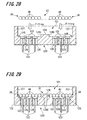
- FIG. 26 through FIG. 34 show a schematic configuration of principal portions of a magnetic layer formation device 120 and the magnetic layer formation processes in which, by injecting a magnetic solution, a magnetic layer can be formed on a planar portion and on the side-face portion of a planar coil.
- FIG. 26 , and FIGS. 28 through 33 are schematic cross-sectional views, seen from a side, of the magnetic layer formation device 120.
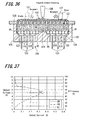
- FIG. 27 is a schematic front view of the magnetic layer formation device 120, seen from the side from which the planar coil is fitted.
- FIG. 34 shows a state in which a magnetic layer is formed on a planar coil using the magnetic layer formation processes of this embodiment.
- the number, positioning, and shapes of the plurality of ejection pins are examples, and the invention is not limited to these examples.
- a planar coil-fitting portion 121 has a bottom-face portion and an inner-wall portion 127 and is formed into a substantially cylindrical depression of predetermined depth greater than the thickness of the planar coil.
- one planar portion of the planar coil, formed by winding electric wire 40 in a spiral shape, is mounted, with the planar coil positioned.
- the wall portion 127 has the shape substantially similar to the outer-perimeter shape of the planar coil, but has the diameter greater by a predetermined length than the diameter of the outer-periphery portion 38 of the planar coil.
- the predetermined length in the planar coil-fitting portion 121 is a value determined by the thickness of the magnetic layer resulting from application to the outside peripheral portion (side-face portion of the planar coil) of the electric wire 40 on the outer periphery 38 of the planar coil.
- the predetermined depth is a value determined by the thickness of the magnetic layer applied onto the electric wire 40 in the planar portion of the planar coil.
- a cylindrical-shape protruding portion 124 In the center portion of the bottom-face portion of the cylindrical depression of the planar coil-fitting portion 121.
- the cylindrical-shape protruding portion 124 determines the planar coil fitting position and has an outer-periphery portion 124C of diameter substantially close contact with the inner-periphery portion 37 of the planar coil (with diameter slightly smaller than the diameter of the inner-periphery portion 37), when the planar coil is fitted. Moreover, the cylindrical-shape protruding portion 124 is lower by a predetermined thickness than the thickness of the planar coil.
- the predetermined thickness in this planar coil-fitting portion 121 is a value determined by the thickness of the magnetic layer applied so as to fill the inner-periphery portion 37 of the planar coil.
- a circular protruding portion 125 determines the planar coil fitting position.
- the circular protruding portion 125 is lower by a predetermined thickness than the planar coil thickness and has a curved shape such that, when the planar coil is loaded, the electric wire 40 on the side of the outer periphery 38 of the planar coil is substantially in close contact from the circular-shape contact position contact with the bottom-face portion to the outer-periphery portion of the electric wire 40, that is, to the end of the outer-periphery portion 38 of the planar coil.
- the predetermined thickness in the planar coil-fitting portion 121 is a value which determines the magnetic layer height on the side of the outer periphery 38 of the planar coil from the plane position of the magnetic layer applied to the planar portion of the planar coil.
- a plurality of ejection pin portions are provided in the bottom-face portion of the planar coil-fitting portion 121.
- Each of the plurality of ejection pins has an ejection pin head 122, ejection pin column 123, and ejection pin hole 126.
- the ejection pin holes 126 are, for example, cylindrical in shape, and are formed so as to penetrate from the bottom-face portion of the planar coil-fitting portion 121 to the bottom portion of the magnetic layer formation device 120.
- the ejection pin heads 122 have diameter slightly smaller than the diameter of the ejection pin holes 126 in the bottom-face portion of the planar coil-fitting portion 121, and are of cylindrical shape having an outer periphery which slides against the inner wall of the ejection pin holes 126.
- the diameter of the cylindrical shape of the ejection pin hole 126 is made to be the same diameter from the bottom-face portion of the planar coil-fitting portion 121 to the bottom portion of the magnetic layer formation device 120.
- the diameter on the side lower than the portion in which the ejection pin heads 122 match the bottom portion of the planar coil-fitting portion 121 may be smaller than the outer-periphery diameter of the ejection pin heads 122 (and may be larger than the diameter of the ejection pin columns 123). Accordingly, plane positioning such that the head plane position of the ejection pin heads 122 is substantially the same as the bottom-face plane position of the planar coil-fitting portion 121 is possible, and the ejection pin heads 122 can be prevented from falling into the bottom side of the magnetic layer formation device 120.
- the ejection pin column 123 is formed from a column-shaped member such that one end is fixed to the rear face of an ejection pin head 122 (the face opposite the side of the bottom portion of the planar coil-fitting portion 121), and the other end is formed to protrude from the bottom portion of the magnetic layer formation device 120.
- the other ends of the ejection pin columns 123 are capable of pressing the ejection pin columns 123 into the side of the planar coil-fitting portion 121 if necessary, using an ejection mechanism, not shown.
- the following process is carried out as a first process.
- the head plane positions of the respective ejection pin heads 122 are positioned so as to be substantially in the same plane as the bottom-face plane position of the planar coil-fitting portion 121, as shown in FIG. 28 and FIG. 29 .
- the inner-periphery portion 37 of the planar coil is fitted in substantially close contact with the outer-periphery portion 124C of the cylindrical protruding portion 124 of the planar coil-fitting portion 121.
- the outer-periphery portion 38 of the planar coil is fitted in substantially close contact with the curved shape of the cylindrical protruding portion 125 of the planar coil-fitting portion 121.
- a magnetic solution injection mechanism is positioned above an aperture of the planar coil-fitting portion 121 in the state in which the planar coil is fitted.
- a predetermined amount of magnetic solution 131 is injected into the planar coil-fitting portion 121.
- the predetermined amount of magnetic solution 131 injected by the magnetic solution injection mechanism 130 is an amount which determines the thickness of the magnetic layer on the planar coil after a compression-molding process and a drying process, which are subsequent processes.
- the magnetic solution 131 within the planar coil-fitting portion 121 is compression-molded until the magnetic solution 131 within the planar coil-fitting portion 121 reaches a predetermined height (thickness) from the bottom face of the planar coil-fitting portion 121.
- the compression-molding mechanism 132 is formed in, for example, a cylindrical shape and has an outer periphery of diameter slightly smaller than the diameter of the inner-wall portion 127 of the planar coil-fitting portion 121. The outer periphery slides along the wall face of the inner-wall portion 127 of the planar coil-fitting portion 121.
- the predetermined height (thickness) of the magnetic solution 131 after compression-molding by the compression-molding mechanism 132 is an amount which determines the thickness of the magnetic layer on the planar coil after the drying process, which is a subsequent process. Then, when compression-molding to the predetermined height is completed, the compression-molding mechanism 132 is removed, and thereafter an ejection mechanism, not shown, is used to press the other ends of the ejection pin columns 123 toward the side of the planar coil-fitting portion 121. As a result, the planar coil, in a state in which the compression-molded magnetic solution 131 has been applied, is removed from the planar coil-fitting portion 121.
- the planar coil which has been removed is sent to a drying process, which is the fourth process.
- the magnetic solution 131 in the state of being applied onto the planar coil is dried by a drying mechanism 133.
- the volatile matter in the magnetic solution evaporates, so that the ferrite powder or other magnetic metal powder remains in a state of close adhesion to the planar coil, and the magnetic layer 100 is formed.
- FIG. 26 through FIG. 34 explains a device and processes of using a magnetic solution injection mechanism 130 to inject a magnetic solution and form a magnetic layer.
- a magnetic solution formation device can use a screen application method to apply the magnetic solution and form a magnetic layer on a planar portion and side-face portion of a planar coil.
- FIG. 35 and FIG. 36 are schematic cross-sectional views, seen from a side, of a magnetic layer formation device 120.
- the first process, the third process and the fourth process are similar to the processes described above, and so drawings and explanations of these processes are omitted. Specifically, fitting the planar coil into the planar coil-fitting portion 121, removing the coil after compression-molding of the magnetic solution in the planar coil-fitting portion 121 using a compression-molding mechanism 132, and drying the magnetic solution in the state of being applied onto the removed planar coil to form the magnetic layer in a state of deposition, are not described here.
- a porous screen 135, magnetic solution dispenser 136, and blade mechanism 137 are positioned above the aperture of the planar coil-fitting portion 121 in the state in which the planar coil is fitted, as shown in FIG. 35 and FIG. 36 .
- the porous screen 135 is a sheet-shaped utensil in which numerous minute holes are opened, and is positioned so as to cover the aperture of the planar coil-fitting portion 121.
- the magnetic solution is dispensed from the magnetic solution dispenser 136 onto the porous screen 135 covering the planar coil-fitting portion 121.
- the blade mechanism 137 is moved over the porous screen 135, to cause the magnetic solution which has been dispensed from the magnetic solution dispenser 136 onto the porous screen 135 to be pressed into the minute holes of the porous screen 135 and to drip down from the minute holes into the planar coil-fitting portion 121. Accordingly, the magnetic solution which has passed through the minute holes of the porous screen 135 is injected evenly into the planar coil-fitting portion 121.
- the third process described above is performed.
- magnetic solution is injected by a magnetic solution injection mechanism 130, so that concentration irregularities occur within the magnetic layer formed on the planar coil.
- the device configuration and processes can be made extremely simple, and as the magnetic powder in the magnetic solution, magnetic powder having large particle diameters, which is an extremely effective means of raising the relative permeability, can be used.
- FIG. 37 to FIG. 39 show the relationship between a bridge-connected magnetic path between planar coils and the output voltage and transmission efficiency, measured when determining the value of the relative permeability of the magnetic layer in this embodiment.
- the dashed lines BR in FIG. 37 through FIG. 39 describe the output voltage versus output current characteristic for the bridge-connected magnetic path; the dot-dot-dash lines OV describe the changes in output voltage; and the dot-dash lines EF in the figures describe the transmission efficiency characteristics.
- FIG. 37 shows an example in which the permeability of the magnetic layer is 30;
- FIG. 38 shows an example in which the permeability of the magnetic layer is 50; and
- FIG. 39 shows an example in which the permeability of the magnetic layer is 70.
- an output voltage of approximately 4.5 V to 5.5 V and an output current of approximately 0.4 A to 0.6 A may be necessary, and so a magnetic layer with a high permeability may be used.
- the concentration of the magnetic material relative to the binder solvent is adjusted.
- the magnetic solution used with the above-described magnetic layer formation device and magnetic layer formation processes there is used such magnetic solution that the relative permeability of the magnetic layer after formation on the planar coil is 50 or higher.
- the noncontact power-transmission coil has functions of only transmitting power or receiving the power; but this invention can be applied to a noncontact power-transmission coil which is provided with functions for both power transmission and for power reception.
- a mobile phone unit 2 and cradle 1 are combined.
- the invention is not limited to such a combination and, for example, application to planar coils used in combinations of a PDA (Personal Digital Assistant) or various other portable terminals with cradles, as well as to noncontact IC cards and reader/writers therefore, and similar are also possible.
- PDA Personal Digital Assistant
Landscapes
- Engineering & Computer Science (AREA)
- Power Engineering (AREA)
- Computer Networks & Wireless Communication (AREA)
- Manufacturing & Machinery (AREA)
- Charge And Discharge Circuits For Batteries Or The Like (AREA)
- Coils Or Transformers For Communication (AREA)
- Secondary Cells (AREA)
Applications Claiming Priority (1)
| Application Number | Priority Date | Filing Date | Title |
|---|---|---|---|
| JP2007001642A JP4960710B2 (ja) | 2007-01-09 | 2007-01-09 | 無接点電力伝送コイル、携帯端末及び端末充電装置、平面コイルの磁性体層形成装置及び磁性体層形成方法 |
Publications (3)
| Publication Number | Publication Date |
|---|---|
| EP1947660A2 true EP1947660A2 (de) | 2008-07-23 |
| EP1947660A3 EP1947660A3 (de) | 2014-10-15 |
| EP1947660B1 EP1947660B1 (de) | 2017-03-08 |
Family
ID=39495938
Family Applications (1)
| Application Number | Title | Priority Date | Filing Date |
|---|---|---|---|
| EP08250066.1A Active EP1947660B1 (de) | 2007-01-09 | 2008-01-08 | Kontaktlose Leistungsübertragungsspule, tragbares Endgerät und Endgerätladevorrichtung, Flachspulenvorrichtung zur Bildung einer Magnetschicht und Verfahren zur Bildung einer Magnetschicht |
Country Status (4)
| Country | Link |
|---|---|
| US (1) | US8072304B2 (de) |
| EP (1) | EP1947660B1 (de) |
| JP (1) | JP4960710B2 (de) |
| CN (1) | CN101304183B (de) |
Cited By (7)
| Publication number | Priority date | Publication date | Assignee | Title |
|---|---|---|---|---|
| WO2011031473A3 (en) * | 2009-08-25 | 2011-06-23 | Access Business Group International Llc | Flux concentrator and method of making a magnetic flux concentrator |
| CN102593896A (zh) * | 2012-02-16 | 2012-07-18 | 华为终端有限公司 | 移动终端及移动终端无线充电的方法 |
| EP2546843A4 (de) * | 2010-03-09 | 2014-06-11 | Nitto Denko Corp | Magentisches element zur drahtlosen stromübertragung und stromversorgungsvorrichtung |
| EP2750145A1 (de) * | 2012-12-28 | 2014-07-02 | Samsung Electro-Mechanics Co., Ltd | Spule für kabelloses Laden und kabellose Ladevorrichtung damit |
| EP2795641A1 (de) * | 2011-12-22 | 2014-10-29 | DSM IP Assets B.V. | Induktives drahtloses aufladesystem |
| CN104467124A (zh) * | 2014-12-31 | 2015-03-25 | 深圳市泰金田科技有限公司 | 地埋式电动汽车无线充电装置 |
| GB2551990A (en) * | 2016-07-04 | 2018-01-10 | Bombardier Primove Gmbh | Transferring energy by magnetic induction using a primary unit conductor arrangement and a layer comprising magnetic and/or magnetizable material |
Families Citing this family (97)
| Publication number | Priority date | Publication date | Assignee | Title |
|---|---|---|---|---|
| JP5266665B2 (ja) * | 2007-05-16 | 2013-08-21 | セイコーエプソン株式会社 | 電子機器、充電器および充電システム |
| JP4900077B2 (ja) * | 2007-06-20 | 2012-03-21 | パナソニック電工株式会社 | 非接触電力伝送機器 |
| US20110133691A1 (en) * | 2007-11-20 | 2011-06-09 | Nokia Corporation | Wireless Galvanic Charging Device,Method of Operation Thereof and Mobile Electric Device to be Charged |
| KR100933864B1 (ko) * | 2008-03-31 | 2009-12-24 | 삼성에스디아이 주식회사 | 배터리 팩 |
| US7855529B2 (en) * | 2008-07-16 | 2010-12-21 | ConvenientPower HK Ltd. | Inductively powered sleeve for mobile electronic device |
| CN201252539Y (zh) * | 2008-09-12 | 2009-06-03 | 汪玉华 | 手机和蓝牙耳机放置和充电的支架 |
| JP4849142B2 (ja) * | 2009-02-27 | 2012-01-11 | ソニー株式会社 | 電力供給装置および電力伝送システム |
| US11476566B2 (en) | 2009-03-09 | 2022-10-18 | Nucurrent, Inc. | Multi-layer-multi-turn structure for high efficiency wireless communication |
| JP5689587B2 (ja) * | 2009-03-31 | 2015-03-25 | 富士通株式会社 | 電力伝送装置 |
| US20140211360A1 (en) * | 2009-06-02 | 2014-07-31 | Correlated Magnetics Research, Llc | System and method for producing magnetic structures |
| WO2011001812A1 (ja) * | 2009-06-30 | 2011-01-06 | 株式会社村田製作所 | コイル、コイルの製造方法、及びコイルモジュール |
| USD611898S1 (en) | 2009-07-17 | 2010-03-16 | Lin Wei Yang | Induction charger |
| USD611899S1 (en) | 2009-07-31 | 2010-03-16 | Lin Wei Yang | Induction charger |
| USD611900S1 (en) | 2009-07-31 | 2010-03-16 | Lin Wei Yang | Induction charger |
| WO2011024621A1 (ja) | 2009-08-25 | 2011-03-03 | 株式会社村田製作所 | 電池パック |
| EP2476179B1 (de) * | 2009-09-09 | 2017-07-05 | Philips Lighting Holding B.V. | Elektronische vorrichtung sowie ein basisteil und ein elektronisches bauteil für die anwendung in derartiger elektronischen vorrichtung |
| GB2488086B (en) | 2010-01-05 | 2014-11-05 | Access Business Group Int Llc | Inductive charging system for electric vehicle |
| JP2011187559A (ja) * | 2010-03-05 | 2011-09-22 | Tsuchiya Co Ltd | 非接触電力伝送フィルム |
| JP2011210937A (ja) * | 2010-03-30 | 2011-10-20 | Murata Mfg Co Ltd | コイルモジュール、及び該コイルモジュールを備えた電子機器 |
| JP5530783B2 (ja) * | 2010-03-31 | 2014-06-25 | 日本写真印刷株式会社 | コイルを備えた成形品の製造方法 |
| KR101806955B1 (ko) * | 2010-05-19 | 2017-12-11 | 삼성전자주식회사 | 휴대 단말기의 무접점 충전 장치 |
| WO2012101729A1 (ja) * | 2011-01-26 | 2012-08-02 | パナソニック株式会社 | 非接触充電モジュール及び非接触充電機器 |
| US20120274148A1 (en) * | 2011-04-27 | 2012-11-01 | Samsung Electro-Mechanics Co., Ltd. | Contactless power transmission device and electronic device having the same |
| JP5457478B2 (ja) * | 2011-06-14 | 2014-04-02 | パナソニック株式会社 | 携帯端末 |
| CN103748765B (zh) | 2011-06-14 | 2016-11-09 | 松下电器产业株式会社 | 通信装置 |
| KR101246692B1 (ko) * | 2011-07-14 | 2013-03-21 | 주식회사 한림포스텍 | 무선전력 통신시스템용 전력 전송장치 |
| US10204734B2 (en) | 2011-11-02 | 2019-02-12 | Panasonic Corporation | Electronic device including non-contact charging module and near field communication antenna |
| KR101558311B1 (ko) | 2011-11-02 | 2015-10-07 | 파나소닉 주식회사 | 비접촉 무선 통신용 코일, 전송 코일 및 휴대 무선 단말 |
| JP6099020B2 (ja) | 2011-12-14 | 2017-03-22 | パナソニックIpマネジメント株式会社 | 情報伝送装置及びシステム |
| WO2013088640A1 (ja) * | 2011-12-14 | 2013-06-20 | パナソニック株式会社 | 非接触コネクタ装置及びシステム |
| US11967839B2 (en) | 2011-12-30 | 2024-04-23 | Analog Devices, Inc. | Electromagnetic connector for an industrial control system |
| US9727511B2 (en) | 2011-12-30 | 2017-08-08 | Bedrock Automation Platforms Inc. | Input/output module with multi-channel switching capability |
| US8862802B2 (en) * | 2011-12-30 | 2014-10-14 | Bedrock Automation Platforms Inc. | Switch fabric having a serial communications interface and a parallel communications interface |
| US9600434B1 (en) | 2011-12-30 | 2017-03-21 | Bedrock Automation Platforms, Inc. | Switch fabric having a serial communications interface and a parallel communications interface |
| US8971072B2 (en) | 2011-12-30 | 2015-03-03 | Bedrock Automation Platforms Inc. | Electromagnetic connector for an industrial control system |
| US10834094B2 (en) | 2013-08-06 | 2020-11-10 | Bedrock Automation Platforms Inc. | Operator action authentication in an industrial control system |
| US9467297B2 (en) | 2013-08-06 | 2016-10-11 | Bedrock Automation Platforms Inc. | Industrial control system redundant communications/control modules authentication |
| US9191203B2 (en) | 2013-08-06 | 2015-11-17 | Bedrock Automation Platforms Inc. | Secure industrial control system |
| US10834820B2 (en) | 2013-08-06 | 2020-11-10 | Bedrock Automation Platforms Inc. | Industrial control system cable |
| US12061685B2 (en) | 2011-12-30 | 2024-08-13 | Analog Devices, Inc. | Image capture devices for a secure industrial control system |
| US9437967B2 (en) | 2011-12-30 | 2016-09-06 | Bedrock Automation Platforms, Inc. | Electromagnetic connector for an industrial control system |
| JP2013169122A (ja) | 2012-02-17 | 2013-08-29 | Panasonic Corp | 非接触充電モジュール及びそれを備えた携帯端末 |
| KR101339486B1 (ko) * | 2012-03-29 | 2013-12-10 | 삼성전기주식회사 | 박막 코일 및 이를 구비하는 전자 기기 |
| US9325388B2 (en) * | 2012-06-21 | 2016-04-26 | Siemens Energy, Inc. | Wireless telemetry system including an induction power system |
| JP6112383B2 (ja) | 2012-06-28 | 2017-04-12 | パナソニックIpマネジメント株式会社 | 携帯端末 |
| JP6008237B2 (ja) | 2012-06-28 | 2016-10-19 | パナソニックIpマネジメント株式会社 | 携帯端末 |
| JP2014027094A (ja) * | 2012-07-26 | 2014-02-06 | Dexerials Corp | コイルモジュール及び受電装置 |
| US9179558B1 (en) | 2012-09-17 | 2015-11-03 | Brite Case, LLC | Case with panel for display |
| ES2687697T3 (es) * | 2012-10-11 | 2018-10-26 | Arçelik Anonim Sirketi | Un dispositivo de cocina inalámbrico operado sobre un fogón de calentamiento por inducción |
| CN102945742B (zh) * | 2012-11-19 | 2015-12-02 | 深圳顺络电子股份有限公司 | 一种充电线圈组件 |
| KR101343883B1 (ko) | 2012-11-27 | 2013-12-20 | 앰코 테크놀로지 코리아 주식회사 | 무선 충전 패키지 구조와 제조방법 |
| JP6306288B2 (ja) * | 2013-05-13 | 2018-04-04 | 日東電工株式会社 | コイルプリント配線基板、受電モジュール、電池ユニットおよび受電通信モジュール |
| US10613567B2 (en) | 2013-08-06 | 2020-04-07 | Bedrock Automation Platforms Inc. | Secure power supply for an industrial control system |
| KR101532052B1 (ko) * | 2013-08-29 | 2015-06-29 | 주식회사 이랜텍 | 무선충전 및 엔에프씨 통신 겸용 단자부를 포함하는 안테나 패치 |
| JP6095224B2 (ja) * | 2013-10-04 | 2017-03-15 | 新電元工業株式会社 | 非接触給電システム |
| US10090712B2 (en) * | 2014-01-30 | 2018-10-02 | Hewlett-Packard Development Company, L.P. | Wireless power alignment |
| KR101762778B1 (ko) | 2014-03-04 | 2017-07-28 | 엘지이노텍 주식회사 | 무선 충전 및 통신 기판 그리고 무선 충전 및 통신 장치 |
| CN105281061A (zh) | 2014-07-07 | 2016-01-27 | 基岩自动化平台公司 | 工业控制系统电缆 |
| JP5991355B2 (ja) * | 2014-09-02 | 2016-09-14 | 株式会社村田製作所 | コイルモジュール、及び該コイルモジュールを備えた電子機器 |
| JP2016073059A (ja) * | 2014-09-29 | 2016-05-09 | セイコーインスツル株式会社 | 非接触電力伝送装置、非接触電力伝送装置を搭載した電子機器、非接触電力伝送装置の製造方法 |
| US10658847B2 (en) | 2015-08-07 | 2020-05-19 | Nucurrent, Inc. | Method of providing a single structure multi mode antenna for wireless power transmission using magnetic field coupling |
| US10063100B2 (en) | 2015-08-07 | 2018-08-28 | Nucurrent, Inc. | Electrical system incorporating a single structure multimode antenna for wireless power transmission using magnetic field coupling |
| US11205848B2 (en) | 2015-08-07 | 2021-12-21 | Nucurrent, Inc. | Method of providing a single structure multi mode antenna having a unitary body construction for wireless power transmission using magnetic field coupling |
| US10636563B2 (en) | 2015-08-07 | 2020-04-28 | Nucurrent, Inc. | Method of fabricating a single structure multi mode antenna for wireless power transmission using magnetic field coupling |
| WO2017031348A1 (en) | 2015-08-19 | 2017-02-23 | Nucurrent, Inc. | Multi-mode wireless antenna configurations |
| WO2017038797A1 (ja) * | 2015-09-02 | 2017-03-09 | 住友電工プリントサーキット株式会社 | フレキシブルプリント配線板及び非接触充電システム |
| CN112259341A (zh) * | 2015-10-26 | 2021-01-22 | 鲲腾科技有限公司 | 具有自闭合磁路的磁结构 |
| US9872379B2 (en) | 2016-03-16 | 2018-01-16 | Microsoft Technology Licensing Llc | Flexible printed circuit with radio frequency choke |
| US20170287626A1 (en) * | 2016-03-31 | 2017-10-05 | Tyco Electronics Corporation | Coil assembly for wireless power transfer having a shaped flux-control body |
| US9839117B2 (en) | 2016-04-11 | 2017-12-05 | Microsoft Technology Licensing, Llc | Flexible printed circuit with enhanced ground plane connectivity |
| US10756572B2 (en) * | 2016-05-20 | 2020-08-25 | Lear Corporation | Wireless charging pad having coolant assembly |
| US11011915B2 (en) | 2016-08-26 | 2021-05-18 | Nucurrent, Inc. | Method of making a wireless connector transmitter module |
| US10245963B2 (en) | 2016-12-05 | 2019-04-02 | Lear Corporation | Air cooled wireless charging pad |
| EP3552298A4 (de) | 2016-12-09 | 2020-01-15 | NuCurrent, Inc. | Substrat mit konfiguration zur erleichterung der energieübertragung durch metall über eine magnetische nahfeldkopplung |
| US11177695B2 (en) | 2017-02-13 | 2021-11-16 | Nucurrent, Inc. | Transmitting base with magnetic shielding and flexible transmitting antenna |
| JP7190442B2 (ja) * | 2017-04-05 | 2022-12-15 | メドトロニック,インコーポレイテッド | 植込み型医療電気システムを再充電するための組立体およびそのヘッドギア |
| US11277028B2 (en) | 2017-05-26 | 2022-03-15 | Nucurrent, Inc. | Wireless electrical energy transmission system for flexible device orientation |
| US10601330B1 (en) * | 2017-09-06 | 2020-03-24 | Apple Inc. | Tertiary winding for coupled inductor structures |
| JP2019062135A (ja) * | 2017-09-28 | 2019-04-18 | 京セラ株式会社 | 電力伝送用コイル装置、非接触電力伝送システム及び電力伝送用コイル装置の製造方法 |
| WO2020044203A1 (en) * | 2018-08-31 | 2020-03-05 | 3M Innovative Properties Company | Coil and method of making same |
| JP2020053522A (ja) * | 2018-09-26 | 2020-04-02 | 矢崎総業株式会社 | 電力伝送ユニット |
| JP7321726B2 (ja) | 2019-03-12 | 2023-08-07 | 日東電工株式会社 | インダクタ |
| JP7325197B2 (ja) * | 2019-03-12 | 2023-08-14 | 日東電工株式会社 | インダクタ |
| JP7219641B2 (ja) * | 2019-03-12 | 2023-02-08 | 日東電工株式会社 | インダクタ |
| JP7286354B2 (ja) | 2019-03-12 | 2023-06-05 | 日東電工株式会社 | インダクタ |
| JP7294833B2 (ja) | 2019-03-12 | 2023-06-20 | 日東電工株式会社 | インダクタ |
| US11227712B2 (en) | 2019-07-19 | 2022-01-18 | Nucurrent, Inc. | Preemptive thermal mitigation for wireless power systems |
| US11271430B2 (en) | 2019-07-19 | 2022-03-08 | Nucurrent, Inc. | Wireless power transfer system with extended wireless charging range |
| US11056922B1 (en) | 2020-01-03 | 2021-07-06 | Nucurrent, Inc. | Wireless power transfer system for simultaneous transfer to multiple devices |
| US11283303B2 (en) | 2020-07-24 | 2022-03-22 | Nucurrent, Inc. | Area-apportioned wireless power antenna for maximized charging volume |
| US11881716B2 (en) | 2020-12-22 | 2024-01-23 | Nucurrent, Inc. | Ruggedized communication for wireless power systems in multi-device environments |
| US11876386B2 (en) | 2020-12-22 | 2024-01-16 | Nucurrent, Inc. | Detection of foreign objects in large charging volume applications |
| US11695302B2 (en) | 2021-02-01 | 2023-07-04 | Nucurrent, Inc. | Segmented shielding for wide area wireless power transmitter |
| CN214755753U (zh) * | 2021-05-13 | 2021-11-16 | 宁波微鹅电子科技有限公司 | 一种无线充电装置 |
| US11831174B2 (en) | 2022-03-01 | 2023-11-28 | Nucurrent, Inc. | Cross talk and interference mitigation in dual wireless power transmitter |
| US12003116B2 (en) | 2022-03-01 | 2024-06-04 | Nucurrent, Inc. | Wireless power transfer system for simultaneous transfer to multiple devices with cross talk and interference mitigation |
| US20250118476A1 (en) * | 2023-10-05 | 2025-04-10 | Delta Electronics, Inc. | Flex pcb winding with thermal cooling |
Family Cites Families (20)
| Publication number | Priority date | Publication date | Assignee | Title |
|---|---|---|---|---|
| KR890004585B1 (ko) * | 1980-09-11 | 1989-11-16 | 아사히가세이고교가부시키가이샤 | 마이크로코일(microcoil) |
| JP2521818B2 (ja) | 1989-09-01 | 1996-08-07 | キヤノン株式会社 | 出力制御装置 |
| JPH0390371U (de) * | 1989-12-28 | 1991-09-13 | ||
| JP2941484B2 (ja) * | 1991-05-31 | 1999-08-25 | 株式会社東芝 | 平面トランス |
| JPH07263935A (ja) * | 1994-03-24 | 1995-10-13 | Hochiki Corp | アンテナ装置 |
| TW282594B (de) * | 1994-06-30 | 1996-08-01 | Yokogawa Electric Corp | |
| US6103157A (en) * | 1997-07-02 | 2000-08-15 | Ciba Specialty Chemicals Corp. | Process for impregnating electrical coils |
| JPH11103531A (ja) * | 1997-09-29 | 1999-04-13 | Nec Mori Energy Kk | 非接触充電装置 |
| JP2000200725A (ja) * | 1998-12-29 | 2000-07-18 | Tokin Corp | 非接触電力伝送装置 |
| JP4684461B2 (ja) * | 2000-04-28 | 2011-05-18 | パナソニック株式会社 | 磁性素子の製造方法 |
| DE10024824A1 (de) * | 2000-05-19 | 2001-11-29 | Vacuumschmelze Gmbh | Induktives Bauelement und Verfahren zu seiner Herstellung |
| EP1340234A1 (de) * | 2000-11-21 | 2003-09-03 | Koninklijke Philips Electronics N.V. | System, leiterplatte, ladegerät, benutzergerät und vorrichtung |
| KR100606307B1 (ko) * | 2001-05-23 | 2006-07-28 | 안태영 | 인체 이식 기구용 무접촉식 동력 전달 장치 |
| US6501364B1 (en) * | 2001-06-15 | 2002-12-31 | City University Of Hong Kong | Planar printed-circuit-board transformers with effective electromagnetic interference (EMI) shielding |
| US7042325B2 (en) * | 2002-05-31 | 2006-05-09 | International Rectifier Corporation | Planar transformer arrangement |
| JP2004047700A (ja) * | 2002-07-11 | 2004-02-12 | Jfe Steel Kk | 非接触充電器用平面磁気素子 |
| JP4852829B2 (ja) | 2004-07-28 | 2012-01-11 | セイコーエプソン株式会社 | 非接触電力伝送装置 |
| US6996892B1 (en) * | 2005-03-24 | 2006-02-14 | Rf Micro Devices, Inc. | Circuit board embedded inductor |
| JP2006339329A (ja) * | 2005-06-01 | 2006-12-14 | Seiko Epson Corp | 平面コイル装置及び基板並びに平面コイル固定方法 |
| JP4947637B2 (ja) * | 2007-01-09 | 2012-06-06 | ソニーモバイルコミュニケーションズ株式会社 | 無接点電力伝送コイル、携帯端末及び端末充電装置 |
-
2007
- 2007-01-09 JP JP2007001642A patent/JP4960710B2/ja active Active
-
2008
- 2008-01-07 US US12/007,077 patent/US8072304B2/en active Active
- 2008-01-08 EP EP08250066.1A patent/EP1947660B1/de active Active
- 2008-01-09 CN CN2008101277942A patent/CN101304183B/zh active Active
Cited By (14)
| Publication number | Priority date | Publication date | Assignee | Title |
|---|---|---|---|---|
| WO2011031473A3 (en) * | 2009-08-25 | 2011-06-23 | Access Business Group International Llc | Flux concentrator and method of making a magnetic flux concentrator |
| CN102598168A (zh) * | 2009-08-25 | 2012-07-18 | 捷通国际有限公司 | 通量集中器和制作磁通量集中器的方法 |
| US8692639B2 (en) | 2009-08-25 | 2014-04-08 | Access Business Group International Llc | Flux concentrator and method of making a magnetic flux concentrator |
| US9390849B2 (en) | 2010-03-09 | 2016-07-12 | Nitto Denko Corporation | Magnetic element for wireless power transmission and power supply device |
| EP2546843A4 (de) * | 2010-03-09 | 2014-06-11 | Nitto Denko Corp | Magentisches element zur drahtlosen stromübertragung und stromversorgungsvorrichtung |
| EP2795641A1 (de) * | 2011-12-22 | 2014-10-29 | DSM IP Assets B.V. | Induktives drahtloses aufladesystem |
| CN102593896B (zh) * | 2012-02-16 | 2014-12-03 | 华为终端有限公司 | 移动终端及移动终端无线充电的方法 |
| CN102593896A (zh) * | 2012-02-16 | 2012-07-18 | 华为终端有限公司 | 移动终端及移动终端无线充电的方法 |
| EP2750145A1 (de) * | 2012-12-28 | 2014-07-02 | Samsung Electro-Mechanics Co., Ltd | Spule für kabelloses Laden und kabellose Ladevorrichtung damit |
| US9355766B2 (en) | 2012-12-28 | 2016-05-31 | Samsung Electro-Mechanics Co., Ltd. | Coil for cordless charging and cordless charging apparatus using the same |
| CN104467124A (zh) * | 2014-12-31 | 2015-03-25 | 深圳市泰金田科技有限公司 | 地埋式电动汽车无线充电装置 |
| CN104467124B (zh) * | 2014-12-31 | 2017-04-19 | 深圳市泰金田科技有限公司 | 地埋式电动汽车无线充电装置 |
| GB2551990A (en) * | 2016-07-04 | 2018-01-10 | Bombardier Primove Gmbh | Transferring energy by magnetic induction using a primary unit conductor arrangement and a layer comprising magnetic and/or magnetizable material |
| US11179745B2 (en) | 2016-07-04 | 2021-11-23 | Bombardier Primove Gmbh | Manufacturing an arrangement for transferring energy from a primary unit conductor arrangement by a magnetic or an electromagnetic field to a secondary unit conductor arrangement |
Also Published As
| Publication number | Publication date |
|---|---|
| JP2008172873A (ja) | 2008-07-24 |
| US8072304B2 (en) | 2011-12-06 |
| CN101304183A (zh) | 2008-11-12 |
| US20080164844A1 (en) | 2008-07-10 |
| EP1947660B1 (de) | 2017-03-08 |
| EP1947660A3 (de) | 2014-10-15 |
| JP4960710B2 (ja) | 2012-06-27 |
| CN101304183B (zh) | 2012-12-05 |
Similar Documents
| Publication | Publication Date | Title |
|---|---|---|
| EP1947660B1 (de) | Kontaktlose Leistungsübertragungsspule, tragbares Endgerät und Endgerätladevorrichtung, Flachspulenvorrichtung zur Bildung einer Magnetschicht und Verfahren zur Bildung einer Magnetschicht | |
| KR101890326B1 (ko) | 무선전력 전송모듈 및 이를 포함하는 휴대용 보조배터리 | |
| EP2348517B1 (de) | Kontaktlose Leistungsübertragungsspule, tragbares Endgerät und Endgerätladevorrichtung | |
| EP1944851B1 (de) | Ein berührungsloses Ladegerät | |
| US8421574B2 (en) | Contactless power transmission apparatus and a method of manufacturing a secondary side thereof | |
| US20210336488A1 (en) | Non-contact power reception apparatus for non-contact charging and electronic settlement performed in a single portable terminal | |
| CN107482791B (zh) | 受电装置、送电装置及送电系统 | |
| CN203366973U (zh) | 非接触充电模块以及使用该非接触充电模块的接收侧非接触充电设备及发送侧非接触充电设备 | |
| US9653942B2 (en) | Receiver for wireless charging system | |
| US9997952B2 (en) | Wireless charging module and mobile terminal including the same | |
| KR101452093B1 (ko) | 박막 코일, 이를 포함하는 차폐 부재 및 이를 구비하는 무접점 전력 전송 장치 | |
| US20090284341A1 (en) | Coil unit and electronic apparatus using the same | |
| CN203910505U (zh) | 非接触充电模块、电子设备和非接触充电设备 | |
| JP2008294385A (ja) | 非接触電力伝送機器及びその受電用コイルブロックの製造方法 | |
| EP2693454B1 (de) | Stromempfangsspule, stromempfangsvorrichtung und kontaktloses stromübertragungssystem | |
| EP2744119B1 (de) | Drahtloser Leistungsempfänger und Herstellungsverfahren dafür | |
| JP2013541832A (ja) | 無線電源システム及び多層シムアセンブリ | |
| US20130264886A1 (en) | Non-contact power supply system | |
| KR100543779B1 (ko) | 무선주파수 식별기술이 적용된 내장형 배터리팩 및 그내장형 배터리팩이 장착되는 휴대 단말기 | |
| EP3605792A1 (de) | System zur drahtlosen stromübertragung und blechspule | |
| KR20150002044A (ko) | 엔에프씨 통신부를 포함하는 무선충전 식별 배터리팩 | |
| JP2014044994A (ja) | コイルユニット | |
| KR20140067185A (ko) | 엔에프씨통신회로부와 무선충전회로부를 포함하는 이동통신장치 | |
| JP2020123523A (ja) | 電池パック、無線電力伝送システムおよび補聴器 | |
| JP2019040860A (ja) | 電池パック、無線電力伝送システムおよび補聴器 |
Legal Events
| Date | Code | Title | Description |
|---|---|---|---|
| PUAI | Public reference made under article 153(3) epc to a published international application that has entered the european phase |
Free format text: ORIGINAL CODE: 0009012 |
|
| AK | Designated contracting states |
Kind code of ref document: A2 Designated state(s): AT BE BG CH CY CZ DE DK EE ES FI FR GB GR HR HU IE IS IT LI LT LU LV MC MT NL NO PL PT RO SE SI SK TR |
|
| AX | Request for extension of the european patent |
Extension state: AL BA MK RS |
|
| RAP1 | Party data changed (applicant data changed or rights of an application transferred) |
Owner name: SEIKO EPSON CORPORATION Owner name: SONY MOBILE COMMUNICATIONS JAPAN, INC. |
|
| PUAL | Search report despatched |
Free format text: ORIGINAL CODE: 0009013 |
|
| AK | Designated contracting states |
Kind code of ref document: A3 Designated state(s): AT BE BG CH CY CZ DE DK EE ES FI FR GB GR HR HU IE IS IT LI LT LU LV MC MT NL NO PL PT RO SE SI SK TR |
|
| AX | Request for extension of the european patent |
Extension state: AL BA MK RS |
|
| RIC1 | Information provided on ipc code assigned before grant |
Ipc: H01F 38/14 20060101AFI20140908BHEP Ipc: H01F 41/14 20060101ALI20140908BHEP |
|
| 17P | Request for examination filed |
Effective date: 20150325 |
|
| RBV | Designated contracting states (corrected) |
Designated state(s): AT BE BG CH CY CZ DE DK EE ES FI FR GB GR HR HU IE IS IT LI LT LU LV MC MT NL NO PL PT RO SE SI SK TR |
|
| AKX | Designation fees paid |
Designated state(s): DE FR GB |
|
| AXX | Extension fees paid |
Extension state: RS Extension state: MK Extension state: AL Extension state: BA |
|
| GRAP | Despatch of communication of intention to grant a patent |
Free format text: ORIGINAL CODE: EPIDOSNIGR1 |
|
| INTG | Intention to grant announced |
Effective date: 20160802 |
|
| RAP1 | Party data changed (applicant data changed or rights of an application transferred) |
Owner name: SONY MOBILE COMMUNICATIONS, INC. Owner name: SEIKO EPSON CORPORATION |
|
| GRAJ | Information related to disapproval of communication of intention to grant by the applicant or resumption of examination proceedings by the epo deleted |
Free format text: ORIGINAL CODE: EPIDOSDIGR1 |
|
| STAA | Information on the status of an ep patent application or granted ep patent |
Free format text: STATUS: REQUEST FOR EXAMINATION WAS MADE |
|
| GRAR | Information related to intention to grant a patent recorded |
Free format text: ORIGINAL CODE: EPIDOSNIGR71 |
|
| GRAS | Grant fee paid |
Free format text: ORIGINAL CODE: EPIDOSNIGR3 |
|
| STAA | Information on the status of an ep patent application or granted ep patent |
Free format text: STATUS: GRANT OF PATENT IS INTENDED |
|
| INTC | Intention to grant announced (deleted) | ||
| INTG | Intention to grant announced |
Effective date: 20161219 |
|
| GRAA | (expected) grant |
Free format text: ORIGINAL CODE: 0009210 |
|
| STAA | Information on the status of an ep patent application or granted ep patent |
Free format text: STATUS: THE PATENT HAS BEEN GRANTED |
|
| AK | Designated contracting states |
Kind code of ref document: B1 Designated state(s): DE FR GB |
|
| REG | Reference to a national code |
Ref country code: GB Ref legal event code: FG4D |
|
| REG | Reference to a national code |
Ref country code: DE Ref legal event code: R096 Ref document number: 602008049056 Country of ref document: DE |
|
| REG | Reference to a national code |
Ref country code: DE Ref legal event code: R097 Ref document number: 602008049056 Country of ref document: DE |
|
| PLBE | No opposition filed within time limit |
Free format text: ORIGINAL CODE: 0009261 |
|
| STAA | Information on the status of an ep patent application or granted ep patent |
Free format text: STATUS: NO OPPOSITION FILED WITHIN TIME LIMIT |
|
| REG | Reference to a national code |
Ref country code: FR Ref legal event code: PLFP Year of fee payment: 11 |
|
| 26N | No opposition filed |
Effective date: 20171211 |
|
| REG | Reference to a national code |
Ref country code: DE Ref legal event code: R082 Ref document number: 602008049056 Country of ref document: DE Representative=s name: DENNEMEYER & ASSOCIATES S.A., DE Ref country code: DE Ref legal event code: R082 Ref document number: 602008049056 Country of ref document: DE Representative=s name: D YOUNG & CO LLP, DE |
|
| REG | Reference to a national code |
Ref country code: DE Ref legal event code: R082 Ref document number: 602008049056 Country of ref document: DE Representative=s name: DENNEMEYER & ASSOCIATES S.A., DE Ref country code: DE Ref legal event code: R081 Ref document number: 602008049056 Country of ref document: DE Owner name: SEIKO EPSON CORPORATION, JP Free format text: FORMER OWNERS: SEIKO EPSON CORPORATION, TOKYO, JP; SONY MOBILE COMMUNICATIONS INC., TOKYO, JP Ref country code: DE Ref legal event code: R082 Ref document number: 602008049056 Country of ref document: DE Representative=s name: DENNEMEYER & ASSOCIATES RECHTSANWALTSGESELLSCH, DE |
|
| REG | Reference to a national code |
Ref country code: GB Ref legal event code: 732E Free format text: REGISTERED BETWEEN 20241003 AND 20241009 |
|
| REG | Reference to a national code |
Ref country code: GB Ref legal event code: 732E Free format text: REGISTERED BETWEEN 20241010 AND 20241016 |
|
| REG | Reference to a national code |
Ref country code: DE Ref legal event code: R082 Ref document number: 602008049056 Country of ref document: DE Representative=s name: DENNEMEYER & ASSOCIATES RECHTSANWALTSGESELLSCH, DE |
|
| PGFP | Annual fee paid to national office [announced via postgrant information from national office to epo] |
Ref country code: GB Payment date: 20260123 Year of fee payment: 19 |
|
| PGFP | Annual fee paid to national office [announced via postgrant information from national office to epo] |
Ref country code: DE Payment date: 20260121 Year of fee payment: 19 |
|
| PGFP | Annual fee paid to national office [announced via postgrant information from national office to epo] |
Ref country code: FR Payment date: 20260123 Year of fee payment: 19 |