EP1935213B1 - Procede pour faire fonctionner un systeme de chauffage par induction - Google Patents
Procede pour faire fonctionner un systeme de chauffage par induction Download PDFInfo
- Publication number
- EP1935213B1 EP1935213B1 EP06806263A EP06806263A EP1935213B1 EP 1935213 B1 EP1935213 B1 EP 1935213B1 EP 06806263 A EP06806263 A EP 06806263A EP 06806263 A EP06806263 A EP 06806263A EP 1935213 B1 EP1935213 B1 EP 1935213B1
- Authority
- EP
- European Patent Office
- Prior art keywords
- voltage
- wave
- induction coil
- transistor
- intermediate circuit
- Prior art date
- Legal status (The legal status is an assumption and is not a legal conclusion. Google has not performed a legal analysis and makes no representation as to the accuracy of the status listed.)
- Active
Links
- 230000006698 induction Effects 0.000 title claims abstract description 40
- 238000000034 method Methods 0.000 title claims abstract description 26
- 238000010438 heat treatment Methods 0.000 title claims abstract description 25
- 239000003990 capacitor Substances 0.000 claims abstract description 51
- 238000007599 discharging Methods 0.000 claims description 8
- 230000004913 activation Effects 0.000 claims description 3
- 230000003139 buffering effect Effects 0.000 claims description 3
- 238000010586 diagram Methods 0.000 description 8
- 238000011017 operating method Methods 0.000 description 8
- 230000007704 transition Effects 0.000 description 6
- 230000008569 process Effects 0.000 description 5
- 238000010248 power generation Methods 0.000 description 4
- 238000006243 chemical reaction Methods 0.000 description 2
- 238000005336 cracking Methods 0.000 description 2
- 230000009849 deactivation Effects 0.000 description 2
- 230000002123 temporal effect Effects 0.000 description 2
- 230000003213 activating effect Effects 0.000 description 1
- 238000012544 monitoring process Methods 0.000 description 1
- 230000005855 radiation Effects 0.000 description 1
- 230000007420 reactivation Effects 0.000 description 1
- 238000004513 sizing Methods 0.000 description 1
- 230000000087 stabilizing effect Effects 0.000 description 1
Images


Classifications
-
- H—ELECTRICITY
- H05—ELECTRIC TECHNIQUES NOT OTHERWISE PROVIDED FOR
- H05B—ELECTRIC HEATING; ELECTRIC LIGHT SOURCES NOT OTHERWISE PROVIDED FOR; CIRCUIT ARRANGEMENTS FOR ELECTRIC LIGHT SOURCES, IN GENERAL
- H05B6/00—Heating by electric, magnetic or electromagnetic fields
- H05B6/02—Induction heating
- H05B6/06—Control, e.g. of temperature, of power
- H05B6/062—Control, e.g. of temperature, of power for cooking plates or the like
Definitions
- the invention relates to a method for operating an induction heating device according to the preamble of claim 1.
- an induction coil is subjected to an alternating voltage or an alternating current, whereby eddy currents are induced in a cookware to be heated, which is magnetically coupled to the induction coil.
- the eddy currents cause heating of the cookware.
- the mains input voltage is usually first rectified by means of a rectifier into a DC supply voltage or intermediate circuit voltage and then processed to generate the high-frequency drive voltage by means of one or more switching means, generally insulated gate bipolar transistors (IGBT) ,
- IGBT insulated gate bipolar transistors
- a first converter variant forms a converter in full bridge circuit, in which the induction coil and a capacitor are connected in series between two so-called half bridges.
- the half bridges are each looped between the intermediate circuit voltage and the reference potential.
- the induction coil and the capacitor form a series resonant circuit.
- Another converter variant forms a half-bridge circuit of two IGBTs, wherein the induction coil and two capacitors, which are connected in series between the intermediate circuit voltage and the reference potential, form a series resonant circuit.
- the induction coil is connected to a connection to a connection point of the two capacitors and to its other connection to a connection point of the two IGBTs forming the half-bridge.
- a variant optimized from a cost point of view uses only one switching means or an IGBT, wherein the induction coil and a capacitor form a parallel resonant circuit. Between the output terminals of the rectifier, parallel to the DC link capacitor, the parallel resonant circuit of induction coil and capacitor are connected in series with the IGBT.
- Allen mentioned inverter variants have in common that the link capacitor charges during a first half-wave to an open circuit voltage with an amount of peak value of the AC line voltage, for example, to 325V at a mains AC voltage of 230V, as soon as they are supplied with mains voltage.
- the invention is therefore based on the object to provide a method for operating an induction heater with a converter available that allows reliable, component-saving and quiet operation of the induction heater with low noise radiation.
- the intermediate circuit capacitor is discharged to a threshold value by driving the switching means in a time range before a zero crossing of the AC mains voltage before the induction coil is driven to produce an adjustable heating power, which already during discharge a small heating power supply in an optionally existing cookware.
- the discharge of the intermediate circuit capacitor causes that at a start of a heating process, ie when the induction coil is to deliver heating power to a cookware, the intermediate circuit capacitor is substantially discharged. If at this time the switching means is turned on or conductive, there is no or only a small current pulse through the switching means and the resonant circuit of induction coil and capacitor. Consequently, there is no switch-on noise and the pulse current load of the power components is reduced, which increases their life.
- the actual heating process can be carried out in a conventional manner, for example, the or the switching means can be controlled with a square wave signal with a working frequency and an associated Hätastfood.
- the inverter is consequently started up with small currents or voltages in the area of the zero crossing. With the rise of the half-wave after the zero crossing, the inverter can adjust to its, the set heating power corresponding operating point with a working frequency and a duty cycle.
- the converter is a single-transistor converter.
- the at least one switching means preferably forms the switching means of the single-transistor converter.
- the inverter is designed in full-bridge circuit or half-bridge circuit, wherein the at least one switching means is part of a bridge.
- the time range starts from 1 ms to 5 ms, preferably 2.5 ms, before the zero crossing of the mains alternating voltage.
- the threshold is in a range of 0V to 20V.
- the intermediate circuit capacitor is discharged to 0V. This allows a practically impuls current-free starting of the inverter.
- the at least one switching means is a transistor, in particular an IGBT.
- the transistor for discharging the intermediate circuit capacitor is driven during the discharge such that a linear operating state of the transistor is established. Since the transistor does not completely switch through in this operating mode or this operating state, the DC link capacitor is discharged slowly along the mains half-cycle. The resulting currents through the parallel resonant circuit and the transistor remain relatively low, whereby noise is avoided or significantly reduced.
- the switching means for discharging the DC link capacitor is driven with a pulse width modulated square wave signal.
- the square-wave voltage signal preferably has a frequency in the range from 20 kHz to 50 kHz, in particular 39 kHz, and / or an on / off ratio in the range from 1/300 to 1/500, in particular 1/378.
- the frequency and / or the on / off ratio is preferably adapted to a used IGBT type, its drive voltage, a driver circuit used for generating the drive voltage and / or to a capacitance value of the DC link capacitor.
- the adjustable heating power is generated by means of a half-wave pattern, wherein the intermediate circuit capacitor is discharged before activation of a half-wave.
- a heating power generation With the aid of the half-wave pattern, individual half-waves of the mains alternating voltage are completely blanked out or deactivated, ie not used for heating power generation.
- 1/3-Netzraumwellen Say example, only one of three consecutive half-waves for power supply to the resonant circuit or the induction coil is used or activated. During the remaining two half-cycles, the switching means remains open, ie no power is fed into the resonant circuit.
- a 2/3 mains half-wave operation two out of three consecutive half-waves are used or activated for supplying power to the oscillating circuit or the induction coil.
- power adjustment is done in a conventional manner.
- Line half-wave operation allows finer resolution of power levels over a wide power setting range.
- Such a power setting is particularly advantageous for single-transistor converters.
- an open-circuit voltage for example, 325V at 230V mains voltage, turns on the intermediate circuit capacitor during an inactive half-wave, during which no power is fed into the resonant circuit.
- Fig. 1 shows a circuit diagram of an induction heater in the form of a Eintransistorumrichters EU.
- the induction heating device may also include further, not shown, identically constructed single-transistor converter EU and additional conventional components, such as control elements for power adjustment, etc.
- the single-transistor converter EU comprises a bridge rectifier GL, which generates a DC link voltage UG from an AC input voltage UN of 230V and 50Hz, a buffer or DC link capacitor C1 for stabilizing or buffering the intermediate DC voltage UG connected between output terminals N1 and N2 of the rectifier GL Induction coil L1 and a capacitor C2, which are connected in parallel and form a parallel resonant circuit, a controllable switching means in the form of an IGB transistor T1, which is looped in series with the resonant circuit between the output terminals N1 and N2 of the rectifier GL, a freewheeling diode D1, the is connected in parallel with a collector-emitter path of the IGB transistor T1, and a control unit SE, for example in the form of a microprocessor or a digital signal processor.
- a control unit SE for example in the form of a microprocessor or a digital signal processor.
- the control unit SE carries out the invention, hereinafter with reference to Fig. 2 described operating method for operating the Eintransistorumrichters EU and may include other, not shown actuators and / or sensors, for example, for mains voltage monitoring, include or be coupled with these.
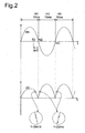
- Fig. 2 does not show true-to-scale timing diagrams of signals from the single-pole converter EU of Fig. 1 , Due to the mains frequency of the input mains AC voltage UN of 50 Hz, a zero crossing takes place every 10 ms between adjacent mains half-waves H1 to H3 of the input mains AC voltage UN.
- the single-transistor converter EU is operated in 2/3 mains half-wave operation, ie power is fed into the parallel resonant circuit or into the induction coil L1 only during two out of three mains half-cycles.
- Fig. 1 Due to the mains frequency of the input mains AC voltage UN of 50 Hz, a zero crossing takes place every 10 ms between adjacent mains half-waves H1 to H3 of the input mains AC voltage UN.
- the single-transistor converter EU is operated in 2/3 mains half-wave operation, ie power is fed into the parallel resonant circuit or into the induction coil L1 only during two out of three mains half-cycles
- the half-waves H2 and H3 are the active half-waves during which power is applied, and the mains half-wave H1 is the inactive half-wave during which no power feed takes place.
- the IGB transistor T1 blocks, except for a transition region or predefinable discharge time range INT, during which the intermediate circuit capacitor C1 is discharged.
- UC is a voltage at the collector of the IGB transistor T1 with respect to a reference potential applied to the terminal N1 of the rectifier GL.
- an open circuit voltage with an amount of a peak value of the mains AC voltage UN at the collector, i. in the illustrated embodiment about 325V.
- the active half waves H2 and H3 power is fed into the induction coil L1.
- This can be effected in a conventional manner, for example by driving the IGB transistor T1 with a square-wave voltage signal having a frequency and a duty cycle, which are adjusted depending on the power to be injected during the half-wave.
- the IGB transistor T1 is driven by a rectangular voltage signal, not shown, with a frequency of about 39 kHz and an on / off ratio of about 1/378.
- the drive pulses are so short that they are insufficient to clear the charge on the IGB transistor gate.
- the IGB transistor T1 is therefore not completely turned on, but goes into a linear operation mode.
- the voltage UC at the collector of the IGB transistor T1 which in this case corresponds to the voltage UG at the intermediate circuit capacitor C1, thereby drops as shown slowly along the network half-wave as an envelope to about 0V.
- the signal UC is shown with greater temporal resolution. From this the switching frequency of the IGBT of approx. 39kHz becomes visible during the discharging process.
- the IGB transistor T1 is driven in a conventional manner with a square-wave voltage signal, not shown.
- Fig. 2 is the envelope of the resulting voltage UC and a partial enlargement of the signal UC shown with greater temporal resolution.
- the voltage UC increases due to the vibration in the parallel resonant circuit to values well above the open circuit voltage.
- the envelope has a sinusoidal shape, which follows the rectified input AC voltage UN.
- the course of the voltage UC shown repeats during the half wave H3.
- the frequency of the drive signal of the IGBT T1 in this operating state is approximately 22 kHz.
- the IGB transistor T1 is deactivated, whereby the voltage UC rises again to its no-load value of approximately 325V.
- the discharge process is repeated, as shown for the half-wave H1. The processes described are repeated periodically.
- the converter circuit can start with small voltages and currents and adjust with the increase of the mains half-wave to its actual operating point of suitable frequency and duty cycle.
- the discharge frequency and duty cycle can be adjusted to operate the IGB transistor in linear mode during discharge.
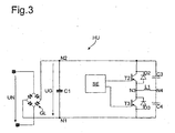
- Fig. 3 shows a circuit diagram of an inverter HU in half-bridge circuit, which is operated with the operating method according to the invention.
- Components with compared to Fig. 1 identical function are the same Provided with reference numerals. Regarding their functional description is on Fig. 1 directed.
- a half-bridge is formed of IGBTs T2 and T3, which are serially connected between the output terminals N1 and N2 of the rectifier GL.
- Freewheeling diodes D2 and D3 are connected in parallel to an associated collector-emitter path of the IGBTs T2 and T3, respectively.
- Capacitors C3 and C4 are also serially connected between the output terminals N1 and N2. Between a connection node N3 of the IGBTs T2 and T3 and a connection node N4 of the capacitors C3 and C4, the induction coil L1 is looped. It forms a series resonant circuit together with the capacitors C3 and C4.
- the IGBTs T2 and T3 are driven by the control unit SE.
- a power setting can be done in a conventional manner, for example by a frequency adjustment of the control signals generated by the control unit SE IGBTs.
- the intermediate circuit capacitor C1 and the capacitors C3 and C4 are discharged by driving the IGBTs T2 and T3.
- This is done analogously to that with reference to Fig. 2 described method by driving the IGBTs T2 and T3 with rectangular voltage signals with a suitable frequency and suitable on / off ratio. Again, the drive pulses are so short that they are insufficient to clear the charge at the respective IGB transistor gate. The IGB transistors T2 and T3 are therefore not completely turned on, but go into a linear operation mode.
- Fig. 4 shows a circuit diagram of an inverter VU in full bridge circuit, which is operated with the operating method according to the invention.
- Components with compared to Fig. 1 identical function are provided with the same reference numerals. Regarding their functional description is on Fig. 1 directed.
- a first half-bridge is formed of IGBTs T4 and T5 and a second half-bridge of IGBTs T6 and T7, which are respectively connected in series between the output terminals N1 and N2 of the rectifier GL.
- Free-wheeling diodes D4 to D7 are connected in parallel with in each case one associated collector-emitter path of the IGBTs T4 to T7.
- the induction coil L1 and a capacitor C5 are connected in series.
- the inductor L1 and the capacitor C5 form a series resonant circuit.
- the IGBTs T4 to T7 are driven by the control unit SE.
- a power setting can be done in a conventional manner, for example by a frequency adjustment of the control signals generated by the control unit SE IGBTs.
- the DC link capacitor C1 is discharged by driving the IGBTs T4 to T7.
- This is done analogously to that with reference to Fig. 2 described method by driving the IGBTs T4 to T7 with square wave signals with a suitable frequency and suitable on / off ratio.
- the drive pulses are again so short that they are not sufficient to clear the charge at the respective IGB transistor gate.
- the IGB transistors T4 to T7 are therefore not completely turned on, but go into a linear operation mode.
- all the IGBTs T4 to T7 or only certain IGBTs can be driven in such a way that a current path for discharging the DC link capacitor C1 is formed.
- a current path for discharging the DC link capacitor C1 is formed.
- only T4 and T5 only T6 and T7, only T4 and T7 or only T6 and T5 for discharge can be controlled.
- the mains voltage is 230V and the mains frequency is 50Hz.
- the operating method shown can be adapted to other mains voltages and mains frequencies.
Landscapes
- Physics & Mathematics (AREA)
- Electromagnetism (AREA)
- Inverter Devices (AREA)
- General Induction Heating (AREA)
- Control Of High-Frequency Heating Circuits (AREA)
- Rectifiers (AREA)
Claims (12)
- Procédé pour servir un dispositif de chauffage par induction comprenant- une bobine d'induction (L1) et- un mutateur (ET, HU, VU) pour la production d'une tension de commande pour la bobine d'induction (L1) avec- un redresseur (GL), qui redresse une tension alternative de réseau (UN),- un condensateur de circuit intermédiaire (C1), bouclé entre les prises de sortie (N1, N2) du redresseur (GL) et qui égalise la tension redressée (UG), et- au moins un dispositif de commutation (de T1 à T7), qui est bouclé entre les prises de sortie (N1, N2) du redresseur (GL),caractérisé en ce que- pendant un laps de temps de décharge (INT) prédéterminable, avant le passage par zéro (ND) de la tension alternative de réseau (UN), le condensateur de circuit intermédiaire (C1) est déchargé jusqu'à une valeur limite par la commande d'un ou de dispositifs de commutation (de T1 à T7), avant que la bobine d'induction (L1) soit commandée pour produire une puissance de chauffage réglable.
- Procédé d'après la revendication 1, caractérisé en ce que le mutateur est un mutateur à un transistor (EU).
- Procédé d'après la revendication 1, caractérisé en ce que le mutateur est un mutateur à circuit en pont intégral (VU) ou en demi-pont (HU), sachant que le ou les dispositifs de commutation (de T1 à T7) font partie d'un pont.
- Procédé d'après une des revendications précédentes, caractérisé en ce que le laps de temps de décharge (INT) commence de 1 ms à 5 ms avant le passage par zéro (ND) de la tension alternative de réseau (UN).
- Procédé d'après une des revendications précédentes, caractérisé en ce que la valeur limite se trouve entre 0V e 20V.
- Procédé d'après une des revendications précédentes, caractérisé en ce que le ou les dispositifs de commutation sont des transistors, notamment des transistors bipolaires à grille isolée - IGBT (de T1 à T/).
- Procédé d'après la revendication 6, caractérisé en ce que pour la décharge du condensateur de circuit intermédiaire (C1), le transistor bipolaire à grille isolée - IGBT (de T1 à T7) est commandé pendant la décharge de manière à obtenir un mode opératoire linéaire des transistors (de T1 à T7).
- Procédé d'après une des revendications précédentes, caractérisé en ce que pour la décharge du condensateur de circuit intermédiaire (C1) le ou les dispositifs de commutation (de T1 à T7) sont commandés par un signal à tension rectangulaire à modulation d'impulsions en largeur.
- Procédé d'après la revendication 8, caractérisé en ce que le signal à tension rectangulaire présente une fréquence entre 20 kHz e 50 kHz.
- Procédé d'après la revendication 8 ou 9, caractérisé en ce que le signal à tension rectangulaire présente un rapport ON/OFF entre 1/300 et 1/500.
- Procédé d'après une des revendications précédentes, caractérisé en ce que la puissance de chauffage réglable est réalisée à l'aide d'un tracé à demi-onde, sachant que le condensateur de circuit intermédiaire (C1) est déchargé avant l'activation d'une demi-onde.
- Procédé d'après la revendication 11, caractérisé en ce qu'on active une sur trois demi-ondes ou bien deux sur trois demi-ondes.
Priority Applications (1)
| Application Number | Priority Date | Filing Date | Title |
|---|---|---|---|
| SI200630281T SI1935213T1 (sl) | 2005-10-14 | 2006-10-13 | Postopek za obratovanje indukcijske grelne priprave |
Applications Claiming Priority (2)
| Application Number | Priority Date | Filing Date | Title |
|---|---|---|---|
| DE102005050038A DE102005050038A1 (de) | 2005-10-14 | 2005-10-14 | Verfahren zum Betrieb einer Induktionsheizeinrichtung |
| PCT/EP2006/009916 WO2007042318A1 (fr) | 2005-10-14 | 2006-10-13 | Procede pour faire fonctionner un systeme de chauffage par induction |
Publications (2)
| Publication Number | Publication Date |
|---|---|
| EP1935213A1 EP1935213A1 (fr) | 2008-06-25 |
| EP1935213B1 true EP1935213B1 (fr) | 2009-01-28 |
Family
ID=37667339
Family Applications (1)
| Application Number | Title | Priority Date | Filing Date |
|---|---|---|---|
| EP06806263A Active EP1935213B1 (fr) | 2005-10-14 | 2006-10-13 | Procede pour faire fonctionner un systeme de chauffage par induction |
Country Status (10)
| Country | Link |
|---|---|
| US (1) | US8415594B2 (fr) |
| EP (1) | EP1935213B1 (fr) |
| JP (1) | JP2009512147A (fr) |
| CN (1) | CN101326857B (fr) |
| AT (1) | ATE422146T1 (fr) |
| CA (1) | CA2625765C (fr) |
| DE (2) | DE102005050038A1 (fr) |
| ES (1) | ES2320594T3 (fr) |
| SI (1) | SI1935213T1 (fr) |
| WO (1) | WO2007042318A1 (fr) |
Cited By (1)
| Publication number | Priority date | Publication date | Assignee | Title |
|---|---|---|---|---|
| WO2022096122A1 (fr) | 2020-11-06 | 2022-05-12 | Intell Properties B.V. | Agencement de circuit pour un appareil de cuisson à induction, appareil de cuisson à induction et procédé de fonctionnement d'un appareil de cuisson à induction |
Families Citing this family (22)
| Publication number | Priority date | Publication date | Assignee | Title |
|---|---|---|---|---|
| EP2034801B1 (fr) * | 2007-09-05 | 2012-10-31 | Whirlpool Corporation | Appareil de cuisson par induction amélioré et procédé pour vérifier les capacités de cuisson d'un appareil de cuisson |
| ES2362523B1 (es) * | 2009-08-27 | 2012-08-02 | BSH Electrodomésticos España S.A. | Control de al menos una carga de calentamiento por inducción. |
| DE102009047185B4 (de) * | 2009-11-26 | 2012-10-31 | E.G.O. Elektro-Gerätebau GmbH | Verfahren und Induktionsheizeinrichtung zum Ermitteln einer Temperatur eines mittels einer Induktionsheizspule erwärmten Kochgefäßbodens |
| ES2386456B1 (es) * | 2010-06-28 | 2013-07-19 | BSH Electrodomésticos España S.A. | Dispositivo de encimera de coccion |
| CN102244949B (zh) * | 2011-06-16 | 2013-04-17 | 美的集团股份有限公司 | 一种电磁加热功率的控制方法 |
| DE102011083383A1 (de) * | 2011-09-26 | 2013-03-28 | E.G.O. Elektro-Gerätebau GmbH | Verfahren zum Beheizen einer in einem Kochgefäß enthaltenen Flüssigkeit und Induktionsheizeinrichtung |
| KR101170804B1 (ko) * | 2012-01-12 | 2012-08-02 | 주식회사 윌링스 | 서지 전류 발생을 방지할 수 있는 공진형 인버터 |
| DE102012207847A1 (de) | 2012-05-10 | 2013-11-14 | Behr-Hella Thermocontrol Gmbh | Vorrichtung zur induktiven Erwärmung eines Heizkörpers |
| CN103731945B (zh) * | 2012-10-11 | 2015-12-02 | 美的集团股份有限公司 | 防止电磁加热装置停振的控制方法及控制电路 |
| US10056774B2 (en) | 2014-02-06 | 2018-08-21 | Mitsubishi Electric Corporation | Discharge device |
| CN106714352B (zh) * | 2015-08-03 | 2019-10-25 | 佛山市顺德区美的电热电器制造有限公司 | 过零导通时间的确定方法、确定系统和电磁加热装置 |
| CN106714353B (zh) * | 2015-08-03 | 2019-11-01 | 佛山市顺德区美的电热电器制造有限公司 | 过零导通时间的确定方法、确定系统和电磁加热装置 |
| EP3177107B1 (fr) * | 2015-12-02 | 2024-01-24 | E.G.O. Elektro-Gerätebau GmbH | Procede de fonctionnement d'une plaque de cuisson a induction |
| ES2684175B1 (es) * | 2017-03-30 | 2019-07-12 | Bsh Electrodomesticos Espana Sa | Dispositivo de aparato domestico y procedimiento para la puesta en funcionamiento de un dispositivo de aparato domestico |
| CN108668394B (zh) * | 2017-03-31 | 2021-10-26 | 佛山市顺德区美的电热电器制造有限公司 | 电磁加热系统及其功率开关管的启动装置和启动方法 |
| CN109047786B (zh) * | 2018-09-25 | 2020-11-24 | 大连理工大学 | 一种纤维状分裂模式下高效制备3d打印用球形金属粉末的装置及方法 |
| EP3768042B1 (fr) * | 2019-07-19 | 2022-12-07 | Electrolux Appliances Aktiebolag | Procédé de commande de l'alimentation en énergie électrique à une bobine d'induction |
| KR20210123045A (ko) | 2020-04-02 | 2021-10-13 | 엘지전자 주식회사 | 공진형 전력 변환 장치의 구동 개시 시 커패시터를 방전시키는 방법 및 그 공진형 전력 변환 장치 |
| DE102020207103A1 (de) | 2020-06-05 | 2021-12-09 | E.G.O. Elektro-Gerätebau GmbH | Verfahren zum Betreiben eines Induktionskochfelds und Induktionskochfeld |
| CN113923810A (zh) * | 2020-07-08 | 2022-01-11 | 台达电子工业股份有限公司 | 加热装置及其控制方法 |
| US11641701B1 (en) * | 2022-08-31 | 2023-05-02 | Techniks, LLC | Electronic protection circuit |
| DE102022210534A1 (de) * | 2022-10-05 | 2024-04-11 | E.G.O. Elektro-Gerätebau GmbH | Vorrichtung zum drahtlosen Übertragen von Energie in Richtung eines Verbrauchers mittels induktiver Kopplung |
Family Cites Families (33)
| Publication number | Priority date | Publication date | Assignee | Title |
|---|---|---|---|---|
| US3569810A (en) * | 1968-11-20 | 1971-03-09 | Allis Chalmers Mfg Co | Pulse width modulator with pulse width limiting |
| DE1928757C3 (de) * | 1969-06-06 | 1978-11-23 | Messer Griesheim Gmbh, 6000 Frankfurt | Schaltungsanordnung zum Stabilisieren und Zünden von Schweißlichtbögen |
| US3787756A (en) * | 1973-01-19 | 1974-01-22 | Pioneer Magnetics Inc | Inrush current limiting circuit |
| CH561285A5 (fr) * | 1973-02-19 | 1975-04-30 | Berghaus Bernhard Elektrophysi | |
| US4277667A (en) * | 1978-06-23 | 1981-07-07 | Matsushita Electric Industrial Co., Ltd. | Induction heating apparatus with negative feedback controlled pulse generation |
| US4438311A (en) * | 1979-07-05 | 1984-03-20 | Sanyo Electric Co., Ltd. | Induction heating cooking apparatus |
| JPS5856475B2 (ja) * | 1979-08-03 | 1983-12-15 | 株式会社東芝 | 誘導加熱調理器の発振回路 |
| JPS5679991U (fr) * | 1979-11-26 | 1981-06-29 | ||
| DE3574903D1 (de) * | 1984-07-14 | 1990-01-25 | Eckerfeld Erika | Elektronischer leistungssteller fuer einen elektrischen durchlauferhitzer mit regelbarer auslauftemperatur. |
| JPH0795471B2 (ja) * | 1986-07-04 | 1995-10-11 | 松下電器産業株式会社 | 誘導加熱調理器 |
| GB2198296B (en) * | 1986-11-25 | 1990-08-08 | Ti Creda Ltd | Improvements in or relating to induction heating circuits for cooking appliances |
| GB2203605B (en) * | 1987-04-07 | 1991-01-09 | Toshiba Kk | Electromagnetic induction heating apparatus capable of preventing undesirable states of cooking utensils or vessels |
| KR900006795B1 (ko) * | 1988-01-29 | 1990-09-21 | 주식회사 금성사 | 전자조리기의 구동 제어방법 |
| US5537074A (en) * | 1993-08-24 | 1996-07-16 | Iversen; Arthur H. | Power semiconductor packaging |
| KR940004040B1 (ko) * | 1991-10-24 | 1994-05-11 | 주식회사 금성사 | 유도가열 조리기의 부하 감지회로 |
| US5354971A (en) * | 1992-07-15 | 1994-10-11 | Chen Su Min | Dual push-pull heating device of induction cooker having multiple burners |
| US5526103A (en) * | 1994-03-31 | 1996-06-11 | Minolta Co., Ltd. | Induction heating fixing device |
| US6118186A (en) * | 1994-09-14 | 2000-09-12 | Coleman Powermate, Inc. | Throttle control for small engines and other applications |
| JPH08196077A (ja) * | 1994-11-18 | 1996-07-30 | Toshiba Corp | 電力変換装置及びこれを利用した空気調和装置 |
| US5648008A (en) * | 1994-11-23 | 1997-07-15 | Maytag Corporation | Inductive cooking range and cooktop |
| US5731681A (en) * | 1995-06-28 | 1998-03-24 | Hitachi Koki Co., Ltd. | Motor control system for centrifugal machine |
| US6021052A (en) * | 1997-09-22 | 2000-02-01 | Statpower Technologies Partnership | DC/AC power converter |
| EP1250029B1 (fr) * | 2000-01-13 | 2010-10-13 | Panasonic Corporation | Rechaud de cuisine par induction |
| JP2002075622A (ja) * | 2000-09-04 | 2002-03-15 | Fuji Electric Co Ltd | 電磁調理器電源 |
| JP3830144B2 (ja) * | 2002-06-21 | 2006-10-04 | 松下電器産業株式会社 | 高周波誘電加熱用電力制御方法およびその装置 |
| EP1432289A1 (fr) * | 2002-12-18 | 2004-06-23 | Harison Toshiba Lighting Corporation | Rouleau chauffé par induction pour un appareil de formation d'images |
| JP2004350493A (ja) * | 2003-04-28 | 2004-12-09 | Matsushita Electric Ind Co Ltd | モータ駆動用インバータ制御装置とこれを用いた空気調和機 |
| JP4148073B2 (ja) * | 2003-08-29 | 2008-09-10 | 富士電機機器制御株式会社 | 誘導加熱装置 |
| JP4117568B2 (ja) * | 2003-09-17 | 2008-07-16 | 三菱電機株式会社 | 誘導加熱調理器 |
| JP4148094B2 (ja) * | 2003-10-15 | 2008-09-10 | 松下電器産業株式会社 | 誘導加熱装置 |
| DE102005050036A1 (de) * | 2005-10-14 | 2007-05-31 | E.G.O. Elektro-Gerätebau GmbH | Induktionsheizeinrichtung und zugehöriges Betriebs- und Topferkennungsverfahren |
| DE102008015036A1 (de) * | 2008-03-14 | 2009-09-17 | E.G.O. Elektro-Gerätebau GmbH | Vorrichtung und Verfahren zur Ansteuerung von Induktionsheizeinrichtungen eines Induktionskochfeldes |
| DE102009047185B4 (de) * | 2009-11-26 | 2012-10-31 | E.G.O. Elektro-Gerätebau GmbH | Verfahren und Induktionsheizeinrichtung zum Ermitteln einer Temperatur eines mittels einer Induktionsheizspule erwärmten Kochgefäßbodens |
-
2005
- 2005-10-14 DE DE102005050038A patent/DE102005050038A1/de not_active Withdrawn
-
2006
- 2006-10-13 ES ES06806263T patent/ES2320594T3/es active Active
- 2006-10-13 DE DE502006002762T patent/DE502006002762D1/de active Active
- 2006-10-13 JP JP2008534942A patent/JP2009512147A/ja active Pending
- 2006-10-13 SI SI200630281T patent/SI1935213T1/sl unknown
- 2006-10-13 CN CN2006800463562A patent/CN101326857B/zh active Active
- 2006-10-13 AT AT06806263T patent/ATE422146T1/de not_active IP Right Cessation
- 2006-10-13 EP EP06806263A patent/EP1935213B1/fr active Active
- 2006-10-13 CA CA2625765A patent/CA2625765C/fr not_active Expired - Fee Related
- 2006-10-13 WO PCT/EP2006/009916 patent/WO2007042318A1/fr active Application Filing
-
2008
- 2008-04-11 US US12/101,419 patent/US8415594B2/en active Active
Cited By (1)
| Publication number | Priority date | Publication date | Assignee | Title |
|---|---|---|---|---|
| WO2022096122A1 (fr) | 2020-11-06 | 2022-05-12 | Intell Properties B.V. | Agencement de circuit pour un appareil de cuisson à induction, appareil de cuisson à induction et procédé de fonctionnement d'un appareil de cuisson à induction |
Also Published As
| Publication number | Publication date |
|---|---|
| US20080203087A1 (en) | 2008-08-28 |
| ES2320594T3 (es) | 2009-05-25 |
| JP2009512147A (ja) | 2009-03-19 |
| CA2625765C (fr) | 2015-06-16 |
| ATE422146T1 (de) | 2009-02-15 |
| CA2625765A1 (fr) | 2007-04-19 |
| WO2007042318A1 (fr) | 2007-04-19 |
| CN101326857A (zh) | 2008-12-17 |
| US8415594B2 (en) | 2013-04-09 |
| EP1935213A1 (fr) | 2008-06-25 |
| DE502006002762D1 (de) | 2009-03-19 |
| CN101326857B (zh) | 2011-11-23 |
| SI1935213T1 (sl) | 2009-08-31 |
| DE102005050038A1 (de) | 2007-05-24 |
Similar Documents
| Publication | Publication Date | Title |
|---|---|---|
| EP1935213B1 (fr) | Procede pour faire fonctionner un systeme de chauffage par induction | |
| EP1935214B1 (fr) | Systeme de chauffage par induction et procede d'utilisation et d'identification de recipient associe | |
| DE10161743B4 (de) | Hochfrequenzanregungsanordnung | |
| DE4040693C2 (fr) | ||
| DE60024215T2 (de) | Modulares hochfrequenz-vorschaltgerät | |
| DE602005003310T2 (de) | Umrichterschaltung für Induktionsheizvorrichtung, Kochgerät mit einer solchen Schaltung und Betriebsverfahren | |
| DE3623306A1 (de) | Entladungslampen-treiber | |
| EP2928265B1 (fr) | Dispositif de chauffage à induction et plaque de cuisson à induction | |
| EP0865150A2 (fr) | Circuit pour la variation continue directe ou indirecte du courant continu et/ou alternatif dans une charge alimentée par une tension de source continue ou alternative ou une combinaison quelconque de ces tensions | |
| EP2469970B1 (fr) | Dispositif d'appareil de cuisson | |
| DE112009002139T5 (de) | Stromversorgungsvorrichtung für eine Elektroerosionsmaschine | |
| CH703021A1 (de) | Schaltungsanordnung für ein induktonskochgerät, verfahren zum betreiben der schaltungsanordnung und induktionskochgerät. | |
| EP3001774A1 (fr) | Dispositif d'appareil menager et procede de fonctionnement d'un dispositif d'appareil menager | |
| WO2007042315A1 (fr) | Systeme de chauffage par induction et procede pour le faire fonctionner | |
| EP3602727B1 (fr) | Dispositif pour appareil ménager et procédé pour faire fonctionner un dispositif pour appareil ménager | |
| EP2469971B1 (fr) | Dispositif d'appareil de cuisson | |
| DE102005038525A1 (de) | Induktionskocheinrichtung mit einstellbarer Heizleistung | |
| EP1355517B1 (fr) | Convertisseur avec découpage à fréquence acoustique | |
| EP2548407B1 (fr) | Dispositif de table de cuisson | |
| EP2506664B1 (fr) | Dispositif d'appareil de cuisson | |
| DE3610196A1 (de) | Kochstelle mit induktiv geheizten kochplatten | |
| DE60113842T2 (de) | Schaltung | |
| EP3422815A1 (fr) | Dispositif de cuisson par induction et procédé de commande d'un dispositif de cuisson par induction | |
| DE102020214810B3 (de) | Verfahren zum Betreiben eines Gleichstrommotors | |
| EP2550841B1 (fr) | Ensemble plaque de cuisson |
Legal Events
| Date | Code | Title | Description |
|---|---|---|---|
| PUAI | Public reference made under article 153(3) epc to a published international application that has entered the european phase |
Free format text: ORIGINAL CODE: 0009012 |
|
| 17P | Request for examination filed |
Effective date: 20080410 |
|
| AK | Designated contracting states |
Kind code of ref document: A1 Designated state(s): AT BE BG CH CY CZ DE DK EE ES FI FR GB GR HU IE IS IT LI LT LU LV MC NL PL PT RO SE SI SK TR |
|
| GRAP | Despatch of communication of intention to grant a patent |
Free format text: ORIGINAL CODE: EPIDOSNIGR1 |
|
| RIN1 | Information on inventor provided before grant (corrected) |
Inventor name: DORWARTH, RALF Inventor name: SCHOENHERR, TOBIAS Inventor name: VOLK, MARTIN Inventor name: SCHILLING, WILFRIED |
|
| DAX | Request for extension of the european patent (deleted) | ||
| GRAS | Grant fee paid |
Free format text: ORIGINAL CODE: EPIDOSNIGR3 |
|
| GRAA | (expected) grant |
Free format text: ORIGINAL CODE: 0009210 |
|
| AK | Designated contracting states |
Kind code of ref document: B1 Designated state(s): AT BE BG CH CY CZ DE DK EE ES FI FR GB GR HU IE IS IT LI LT LU LV MC NL PL PT RO SE SI SK TR |
|
| REG | Reference to a national code |
Ref country code: GB Ref legal event code: FG4D Free format text: NOT ENGLISH |
|
| REG | Reference to a national code |
Ref country code: CH Ref legal event code: EP |
|
| REG | Reference to a national code |
Ref country code: IE Ref legal event code: FG4D Free format text: LANGUAGE OF EP DOCUMENT: GERMAN |
|
| REF | Corresponds to: |
Ref document number: 502006002762 Country of ref document: DE Date of ref document: 20090319 Kind code of ref document: P |
|
| REG | Reference to a national code |
Ref country code: ES Ref legal event code: FG2A Ref document number: 2320594 Country of ref document: ES Kind code of ref document: T3 |
|
| NLV1 | Nl: lapsed or annulled due to failure to fulfill the requirements of art. 29p and 29m of the patents act | ||
| PG25 | Lapsed in a contracting state [announced via postgrant information from national office to epo] |
Ref country code: LT Free format text: LAPSE BECAUSE OF FAILURE TO SUBMIT A TRANSLATION OF THE DESCRIPTION OR TO PAY THE FEE WITHIN THE PRESCRIBED TIME-LIMIT Effective date: 20090128 Ref country code: NL Free format text: LAPSE BECAUSE OF FAILURE TO SUBMIT A TRANSLATION OF THE DESCRIPTION OR TO PAY THE FEE WITHIN THE PRESCRIBED TIME-LIMIT Effective date: 20090128 Ref country code: FI Free format text: LAPSE BECAUSE OF FAILURE TO SUBMIT A TRANSLATION OF THE DESCRIPTION OR TO PAY THE FEE WITHIN THE PRESCRIBED TIME-LIMIT Effective date: 20090128 |
|
| REG | Reference to a national code |
Ref country code: IE Ref legal event code: FD4D |
|
| PG25 | Lapsed in a contracting state [announced via postgrant information from national office to epo] |
Ref country code: PL Free format text: LAPSE BECAUSE OF FAILURE TO SUBMIT A TRANSLATION OF THE DESCRIPTION OR TO PAY THE FEE WITHIN THE PRESCRIBED TIME-LIMIT Effective date: 20090128 Ref country code: LV Free format text: LAPSE BECAUSE OF FAILURE TO SUBMIT A TRANSLATION OF THE DESCRIPTION OR TO PAY THE FEE WITHIN THE PRESCRIBED TIME-LIMIT Effective date: 20090128 Ref country code: SE Free format text: LAPSE BECAUSE OF FAILURE TO SUBMIT A TRANSLATION OF THE DESCRIPTION OR TO PAY THE FEE WITHIN THE PRESCRIBED TIME-LIMIT Effective date: 20090428 Ref country code: PT Free format text: LAPSE BECAUSE OF FAILURE TO SUBMIT A TRANSLATION OF THE DESCRIPTION OR TO PAY THE FEE WITHIN THE PRESCRIBED TIME-LIMIT Effective date: 20090629 Ref country code: IS Free format text: LAPSE BECAUSE OF FAILURE TO SUBMIT A TRANSLATION OF THE DESCRIPTION OR TO PAY THE FEE WITHIN THE PRESCRIBED TIME-LIMIT Effective date: 20090528 |
|
| PG25 | Lapsed in a contracting state [announced via postgrant information from national office to epo] |
Ref country code: IE Free format text: LAPSE BECAUSE OF FAILURE TO SUBMIT A TRANSLATION OF THE DESCRIPTION OR TO PAY THE FEE WITHIN THE PRESCRIBED TIME-LIMIT Effective date: 20090128 Ref country code: EE Free format text: LAPSE BECAUSE OF FAILURE TO SUBMIT A TRANSLATION OF THE DESCRIPTION OR TO PAY THE FEE WITHIN THE PRESCRIBED TIME-LIMIT Effective date: 20090128 Ref country code: DK Free format text: LAPSE BECAUSE OF FAILURE TO SUBMIT A TRANSLATION OF THE DESCRIPTION OR TO PAY THE FEE WITHIN THE PRESCRIBED TIME-LIMIT Effective date: 20090128 Ref country code: CZ Free format text: LAPSE BECAUSE OF FAILURE TO SUBMIT A TRANSLATION OF THE DESCRIPTION OR TO PAY THE FEE WITHIN THE PRESCRIBED TIME-LIMIT Effective date: 20090128 |
|
| PG25 | Lapsed in a contracting state [announced via postgrant information from national office to epo] |
Ref country code: SK Free format text: LAPSE BECAUSE OF FAILURE TO SUBMIT A TRANSLATION OF THE DESCRIPTION OR TO PAY THE FEE WITHIN THE PRESCRIBED TIME-LIMIT Effective date: 20090128 Ref country code: RO Free format text: LAPSE BECAUSE OF FAILURE TO SUBMIT A TRANSLATION OF THE DESCRIPTION OR TO PAY THE FEE WITHIN THE PRESCRIBED TIME-LIMIT Effective date: 20090128 |
|
| PLBE | No opposition filed within time limit |
Free format text: ORIGINAL CODE: 0009261 |
|
| STAA | Information on the status of an ep patent application or granted ep patent |
Free format text: STATUS: NO OPPOSITION FILED WITHIN TIME LIMIT |
|
| 26N | No opposition filed |
Effective date: 20091029 |
|
| PG25 | Lapsed in a contracting state [announced via postgrant information from national office to epo] |
Ref country code: BG Free format text: LAPSE BECAUSE OF FAILURE TO SUBMIT A TRANSLATION OF THE DESCRIPTION OR TO PAY THE FEE WITHIN THE PRESCRIBED TIME-LIMIT Effective date: 20090428 |
|
| BERE | Be: lapsed |
Owner name: E.G.O. ELEKTRO-GERATEBAU G.M.B.H. Effective date: 20091031 |
|
| PG25 | Lapsed in a contracting state [announced via postgrant information from national office to epo] |
Ref country code: MC Free format text: LAPSE BECAUSE OF NON-PAYMENT OF DUE FEES Effective date: 20091031 |
|
| PG25 | Lapsed in a contracting state [announced via postgrant information from national office to epo] |
Ref country code: GR Free format text: LAPSE BECAUSE OF FAILURE TO SUBMIT A TRANSLATION OF THE DESCRIPTION OR TO PAY THE FEE WITHIN THE PRESCRIBED TIME-LIMIT Effective date: 20090429 Ref country code: BE Free format text: LAPSE BECAUSE OF NON-PAYMENT OF DUE FEES Effective date: 20091031 |
|
| PG25 | Lapsed in a contracting state [announced via postgrant information from national office to epo] |
Ref country code: AT Free format text: LAPSE BECAUSE OF NON-PAYMENT OF DUE FEES Effective date: 20091013 |
|
| PG25 | Lapsed in a contracting state [announced via postgrant information from national office to epo] |
Ref country code: LU Free format text: LAPSE BECAUSE OF NON-PAYMENT OF DUE FEES Effective date: 20091013 |
|
| REG | Reference to a national code |
Ref country code: CH Ref legal event code: PL |
|
| PG25 | Lapsed in a contracting state [announced via postgrant information from national office to epo] |
Ref country code: HU Free format text: LAPSE BECAUSE OF FAILURE TO SUBMIT A TRANSLATION OF THE DESCRIPTION OR TO PAY THE FEE WITHIN THE PRESCRIBED TIME-LIMIT Effective date: 20090729 |
|
| PG25 | Lapsed in a contracting state [announced via postgrant information from national office to epo] |
Ref country code: LI Free format text: LAPSE BECAUSE OF NON-PAYMENT OF DUE FEES Effective date: 20101031 Ref country code: CH Free format text: LAPSE BECAUSE OF NON-PAYMENT OF DUE FEES Effective date: 20101031 |
|
| PG25 | Lapsed in a contracting state [announced via postgrant information from national office to epo] |
Ref country code: CY Free format text: LAPSE BECAUSE OF FAILURE TO SUBMIT A TRANSLATION OF THE DESCRIPTION OR TO PAY THE FEE WITHIN THE PRESCRIBED TIME-LIMIT Effective date: 20090128 |
|
| PGFP | Annual fee paid to national office [announced via postgrant information from national office to epo] |
Ref country code: SI Payment date: 20131001 Year of fee payment: 8 |
|
| PG25 | Lapsed in a contracting state [announced via postgrant information from national office to epo] |
Ref country code: SI Free format text: LAPSE BECAUSE OF NON-PAYMENT OF DUE FEES Effective date: 20141014 |
|
| REG | Reference to a national code |
Ref country code: SI Ref legal event code: KO00 Effective date: 20150610 |
|
| REG | Reference to a national code |
Ref country code: FR Ref legal event code: PLFP Year of fee payment: 10 |
|
| REG | Reference to a national code |
Ref country code: FR Ref legal event code: PLFP Year of fee payment: 11 |
|
| REG | Reference to a national code |
Ref country code: FR Ref legal event code: PLFP Year of fee payment: 12 |
|
| REG | Reference to a national code |
Ref country code: FR Ref legal event code: PLFP Year of fee payment: 13 |
|
| PGFP | Annual fee paid to national office [announced via postgrant information from national office to epo] |
Ref country code: GB Payment date: 20231025 Year of fee payment: 18 |
|
| PGFP | Annual fee paid to national office [announced via postgrant information from national office to epo] |
Ref country code: ES Payment date: 20231117 Year of fee payment: 18 |
|
| PGFP | Annual fee paid to national office [announced via postgrant information from national office to epo] |
Ref country code: TR Payment date: 20231004 Year of fee payment: 18 Ref country code: IT Payment date: 20231031 Year of fee payment: 18 Ref country code: FR Payment date: 20231023 Year of fee payment: 18 Ref country code: DE Payment date: 20231018 Year of fee payment: 18 |